Simcom SIM900E GSM/GPRS module User Manual 6 SIM900E
Shanghai Simcom Ltd. GSM/GPRS module 6 SIM900E
Simcom >
SIM900E_User Manual_Rev2

SIM900E Document
- 1 -
User Manual
1. SIM900E Description
1.1. Summarize
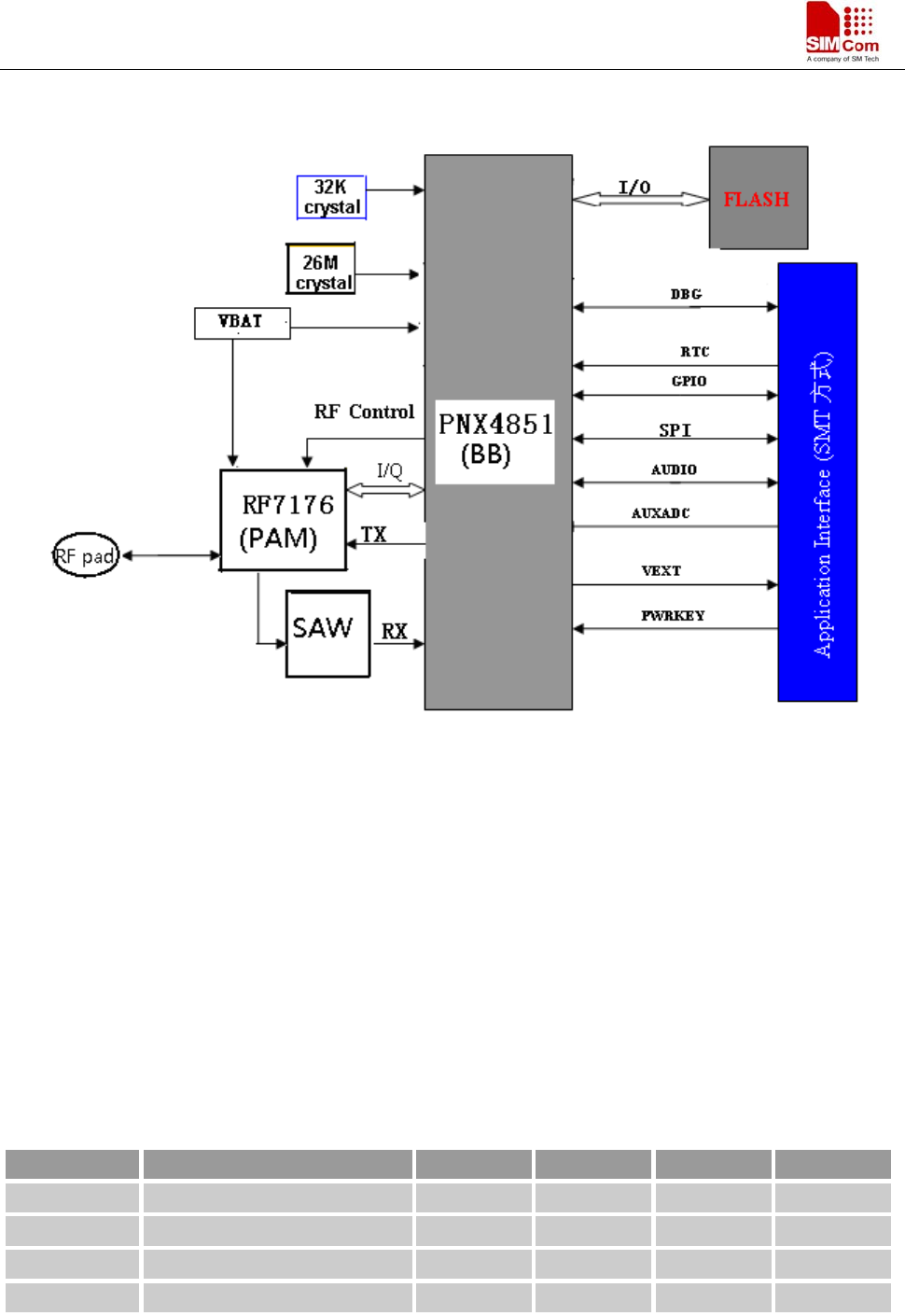
SIM900E designed by SIMCom is a quad-band module which supports GSM/GPRS. The baseband circuit is
based on STE and RF circuit is based on RFMD. It works at quad bands------GSM 850MHz, EGSM 900MHz,
DCS 1800MHz and PCS 1900MHz. CPU clock is based on 26MHz crystal. The main IC includes PNX4851,
RF7176 and Flash, etc.
1.2. Feature
● Quad-band 900/1800/850/1900MHz
● GPRS multi-slot class 10/8
● GPRS mobile station class B
● Compliant to GSM phase 2/2+
– Class 4 (2W) at GSM 850 and EGSM 900
– Class 1 (1W) at DCS 1800 and PCS 1900
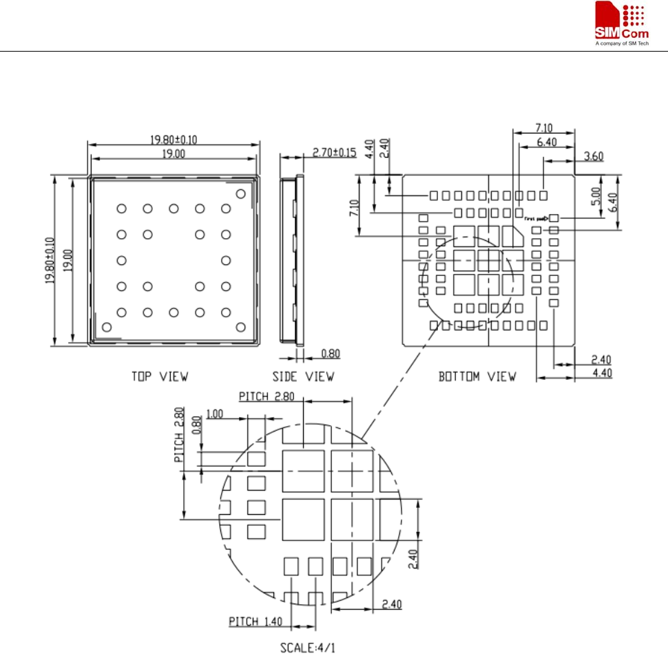
● Dimensions: 19.8*19.8*2.7mm
● Weight: 2.4 g
● Control via AT commands (GSM 07.07 ,07.05 and SIMCom enhanced AT Commands)
● Supply voltage range 3.2V ~ 4.8V
● Low power consumption
● Operation temperature: -30°C ~ +80°C
● 69 SMT pads include
– Interface to external SIM 3V/1.8V
– Analog audio interface
– RTC backup
– Serial interface
– LCD interface
– Antenna pad
– GPIO
– ADC
SIM900E Document
- 2 -
1.3. Pin Name and IO Characters
Pin No. Pin Name I/O
Pin No. Pin Name I/O
1 GND 35 VDD_EXT O
2 SPK_P O 36 PWRKEY I
3 SPK_N O 37 ADC I
4 GND 38
GPIO12 IO
5 MIC_N I 39 SDA IO
6 MIC_P I 40 SCL IO
7 GND 41 DBG_RXD I
8 NETLIGHT O 42 DBG_TXD O
9 GND 43 VRTC IO
10 SIM_CLK O 44 SIM_PRESENCE I
11 SIM_DATA IO 45 GPIO8/KBC2 IO
12 SIM_RST I 46 GPIO1/KBR4 IO
13 SIM_VDD O 47 GPIO9/KBC1 IO
14 STATUS O 48 GPIO6/KBC4 IO
15 NRESET I 49 GPIO7/KBC3 IO
16 RXD I 50 GPIO5/KBR0 IO
17 TXD O 51 GPIO4/KBR1 IO
18 GND 52 GPIO2/KBR3 IO
19 RTS I 53 GPIO3/KBR2 IO
20 CTS O 54 GPIO10 IO
21 DTR I 55 PWM2 O
22 RI O 56 PWM1 O
23 DCD O 57 DISP _CLK O
24 GPIO11 IO 58 DISP _CS O
25 GND 59 DISP_DATA O
26 GND 60 DISP _D/C IO
27 GND 61 GND
28 RF_ANT IO 62 GND
29 GND 63 GND
30 VBAT I 64 GND
31 VBAT I 65 GND
32 VBAT I 66 GND
33 GND 67 GND
34 GND 68 GND
69 GND
SIM900E Document
- 3 -
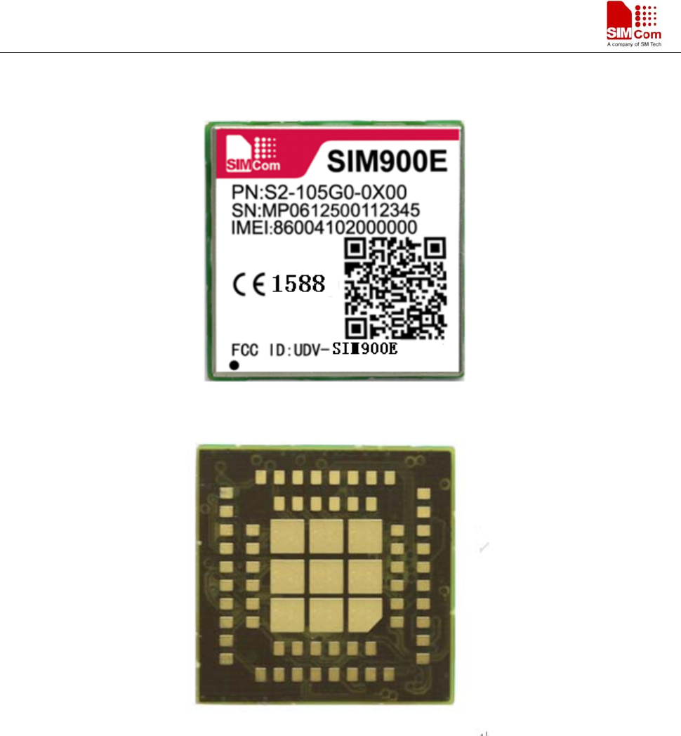
1.4. Pictures
Figure 1: Top view of SIM900E
Figure 2: Bottom view of SIM900E
SIM900E Document
- 4 -
1.5. Dimension
Figure 3: Dimention
SIM900E Document
- 5 -
2. Detail Block Diagram
Figure 4: Block diagram of SIM900E
3. Electrical and Reliability Characteristics
3.1. Absolute Maximum Ratings
The absolute maximum ratings stated in following table are stress ratings under non-operating conditions. Stresses
beyond any of these limits will cause permanent damage to SIM900E .
Table 1: Absolute maximum ratings
Symbol Parameter Min Typ Max Unit
VBAT Power supply voltage - - 5.5 V
VI
* Input voltage -0.3 - 3.1 V
II
* Input current - - 10 mA
IO
* Output current - - 10 mA
*These parameters are for digital interface pins, such as keypad, GPIO, I2C, UART, LCD and DEBUG.
SIM900E Document
- 6 -
3.2. Digital Interface Characteristics
Table 2: Digital interface characteristics
Symbol Parameter Min Typ Max Unit
IIH High-level input current -10 - 10 uA
IIL Low-level input current -10 - 10 uA
VIH High-level input voltage 2.4 - - V
VIL Low-level input voltage - - 0.4 V
VOH High-level output voltage 2.7 - - V
VOL Low-level output voltage - - 0.1 V
* These parameters are for digital interface pins, such as keypad, GPIO, I2C, UART, LCDand DEBUG.
3.3. SIM Card Interface Characteristics
Table 3: SIM card interface characteristics
Symbol Parameter Min Typ Max Unit
IIH High-level input current -10 - 10 uA
IIL Low-level input current -10 - 10 uA
VIH High-level input voltage 1.4 - - V
2.4 - - V
VIL Low-level input voltage - - 0.4 V
2.4 V
VOH High-level output voltage 1.7 - - V
2.7 - - V
VOL Low-level output voltage - - 0.1 V
- - 0.1 V
3.4. SIM_VDD Characteristics
Table 4: SIM_VDD characteristics
Symbol Parameter Min Typ Max Unit
VO Output voltage 2.75 2.9 3.00 V
1.65 1.80 1.95
IO Output current - - 10 mA
SIM900E Document
- 7 -
3.5. VRTC Characteristics
Table 5: VRTC characteristics
Symbol Parameter Min Typ Max Unit
VRTC-IN VRTC input voltage 2.00 3.00 3.15 V
IRTC-IN VRTC input current - 2 - uA
VRTC-OUT VRTC output voltage - 3.00 - V
IRTC-OUT VRTC output current - 10 - uA
3.6. Current Consumption (VBAT = 3.8V)
Table 6: Current consumption
Symbol Parameter Conditions Value Unit
IVRTC VRTC current VBAT disconnects. Backup battery is 3 V 2 uA
IVBAT VBAT current
Power down mode 30 uA
Sleep mode
BS-PA-MFRMS=9 1.0
mA BS-PA-MFRMS=5 1.2
BS-PA-MFRMS=2 1.5
Idle mode
GSM 850
22 mA
EGSM 900
DCS 1800
PCS 1900
Voice call
GSM 850
EGSM 900
PCL=5 240
mA
PCL=12 108
PCL=19 81
DCS 1800
PCS 1900
PCL=0 176
PCL=7 94
PCL=15 76
Data mode
GPRS(1Rx,1Tx)
GSM 850
EGSM 900
PCL=5 240
mA PCL=12 110
PCL=19 83
DCS 1800
PCS 1900
PCL=0 170
mA PCL=7 95
PCL=15 80
Data mode
GPRS(4Rx,1Tx)
GSM 850
EGSM 900
PCL=5 223
mA PCL=12 150
PCL=19 120
SIM900E Document
- 8 -
DCS 1800
PCS 1900
PCL=0 166
mA PCL=7 130
PCL=15 115
Data mode
GPRS(3Rx,2Tx)
GSM 850
EGSM 900
PCL=5 410
mA PCL=12 185
PCL=19 130
DCS 1800
PCS 1900
PCL=0 300
mA PCL=7 155
PCL=15 122
IVBAT-peak Peak current During Tx burst 2 A
3.7. Electro-Static Discharge
SIM900E is an ESD sensitive component, so more attention should be paid to the procedure of handling and
packaging. The ESD test results are shown in the following table.
Table 7: The ESD characteristics (Temperature: 25℃, Humidity: 45 %)
Pin Contact discharge Air discharge
VBAT ±5KV ±10KV
GND ±4KV ±10KV
RXD, TXD ±3KV ±6KV
Antenna port ±5KV ±10KV
SPK_P/ SPK_N
MIC_P/ MIC_N ±2KV ±6KV
PWRKEY ±1KV ±6KV
3.8. Recommended Operating Conditions
Table 8: Recommended operating conditions
Symbol Parameter Min Typ Max Unit
VBAT Power supply voltage 3.6 4.0 4.2 V
TOPER Operating temperature -40 +25 +85 ℃
TSTG Storage temperature -45 +90 ℃
SIM900E Document
- 9 -
4. Radio Characteristics
4.1. Module RF Output Power
The following table shows the module conducted output power, it is followed by the 3GPP TS 05.05 technical
specification requirement.
Table 9: SIM900E GSM850 and EGSM900 conducted RF output power
GSM850 and EGSM900
PCL Nominal output power (dBm) Tolerance (dB) for conditions
Normal Extreme
5 33 ±3 ±4
6 31 ±3 ±4
7 29 ±3 ±4
8 27 ±3 ±4
9 25 ±3 ±4
10 23 ±3 ±4
11 21 ±3 ±4
12 19 ±3 ±4
13 17 ±3 ±4
14 15 ±3 ±4
15 13 ±3 ±4
16 11 ±5 ±6
17 9 ±5 ±6
18 7 ±5 ±6
19-31 5 ±5 ±6
Table 10: SIM900E DCS1800 and PCS1900 conducted RF output power
DCS1800 and PCS1900
PCL Nominal output power (dBm) Tolerance (dB) for conditions
Normal Extreme
0 30 ±3 ±4
1 28 ±3 ±4
2 26 ±3 ±4
3 24 ±3 ±4
4 22 ±3 ±4
5 20 ±3 ±4
6 18 ±3 ±4
SIM900E Document
- 10 -
7 16 ±3 ±4
8 14 ±3 ±4
9 12 ±4 ±5
10 10 ±4 ±5
11 8 ±4 ±5
12 6 ±4 ±5
13 4 ±4 ±5
14 2 ±5 ±6
15-28 0 ±5 ±6
For the module’s output power, the followings should be noted:
At GSM850 and EGSM900 band, the module is a class 4 device, so the module’s output power should not exceed
33dBm, and at the maximum power level, the output power tolerance should not exceed +/-2dB under normal
condition and +/-2.5dB under extreme condition.
At DCS1800 and PCS1900 band, the module is a class 1 device, so the module’s output power should not exceed
30dBm, and at the maximum power level, the output power tolerance should not exceed +/-2dB under normal
condition and +/-2.5dB under extreme condition.
4.2. Module RF Receive Sensitivity
The following table shows the module’s conducted receive sensitivity, it is tested under static condition.
Table 11: SIM900E conducted RF receive sensitivity
Frequency Receive sensitivity(Typical) Receive sensitivity(Max)
GSM850 -109dBm -107dBm
EGSM900 -109dBm -107dBm
DCS1800 -109dBm -107dBm
PCS1900 -109dBm -107dBm
4.3. Module Operating Frequencies
The following table shows the module’s operating frequency range; it is followed by the 3GPP TS 05.05 technical
specification requirement.
Table 12: SIM900E operating frequencies
Frequency Receive Transmit
GSM850 869 ~ 894MHz 824 ~ 849 MHz
EGSM900 925 ~ 960MHz 880 ~ 915MHz
SIM900E Document
- 11 -
DCS1800 1805 ~ 1880MHz 1710 ~ 1785MHz
PCS1900 1930 ~ 1990MHz 1850 ~ 1910MHz
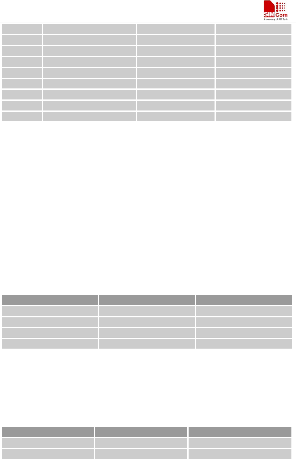
5. RF Circuit Routing Constraints
5.1. General recommendations
To route the RF antenna signals, the following recommendations must be observed for PCB layout: The RF
signals must be routed using traces with a 50 characteristic impedance. Basicaly, the characteristic impedance
depends on the dielectric constant (εr) of the material used, trace width (W), trace thickness (T), and height (H)
between the trace and the reference ground plane. In order to respect this constraint, SIMCom recommends that a
MicroStrip structure be used and trace width be computed with a simulation tool (such as CITS25, shown in the
figure below)
Figure 5: CITS25 screenshot for MicroStrip design power mode diagram
The trace width should be wide enough to maintain reasonable insertion loss and manufacturing reliability.
Cutting out inner layers of ground under the trace will increase the effective substrate height; therefore, increasing
the width of the RF trace.
SIM900E Document
- 12 -
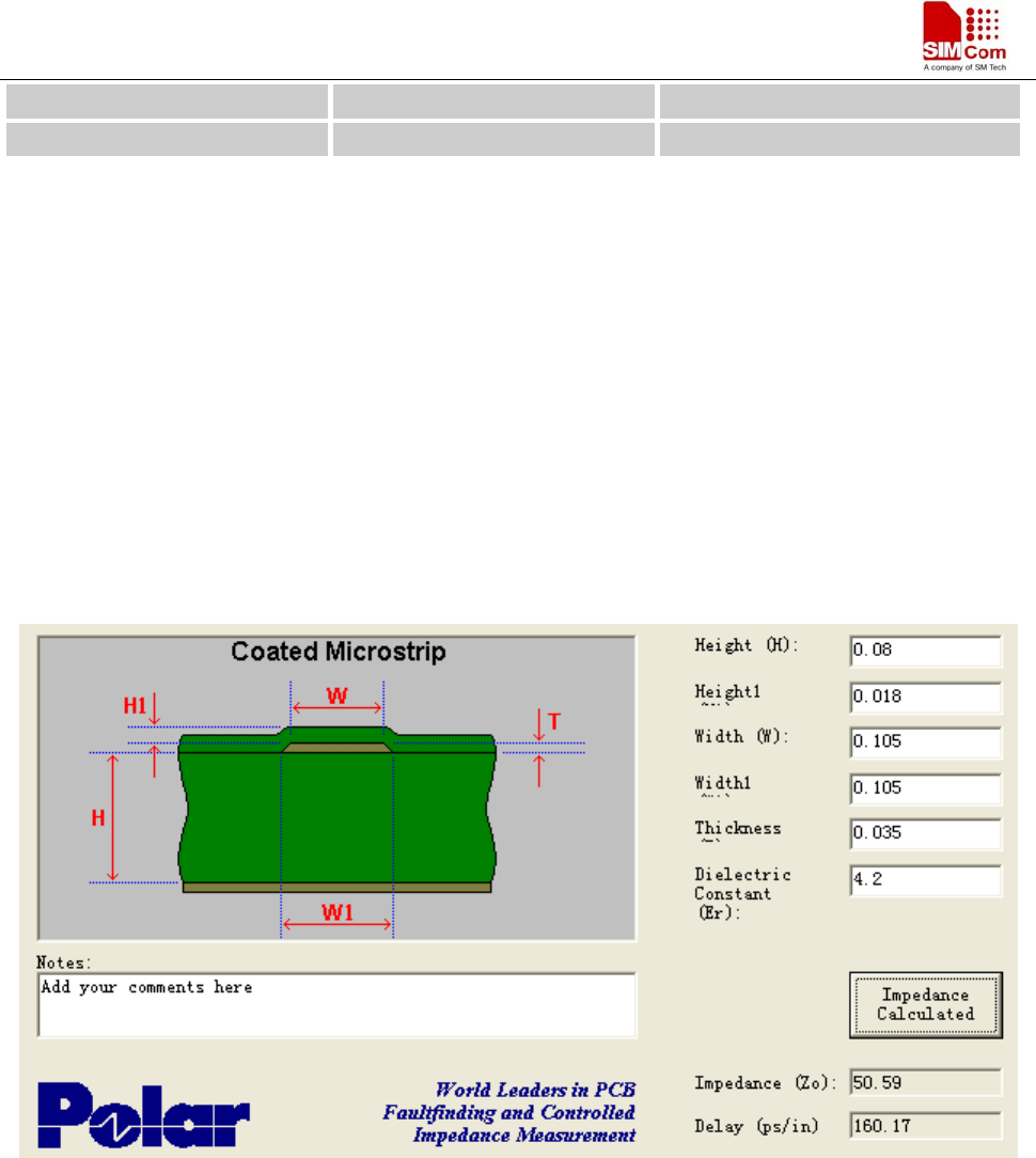
Figure 6: RF routing examples
Fill the area around the RF traces with ground and ground vias to connect inner ground layers
for isolation.
Cut out ground under RF signal pads to reduce stray capacitance losses.
Avoid routing RF traces with sharp corners. A smooth radius is recommended.
The ground reference plane should be a solid continuous plane under the trace.
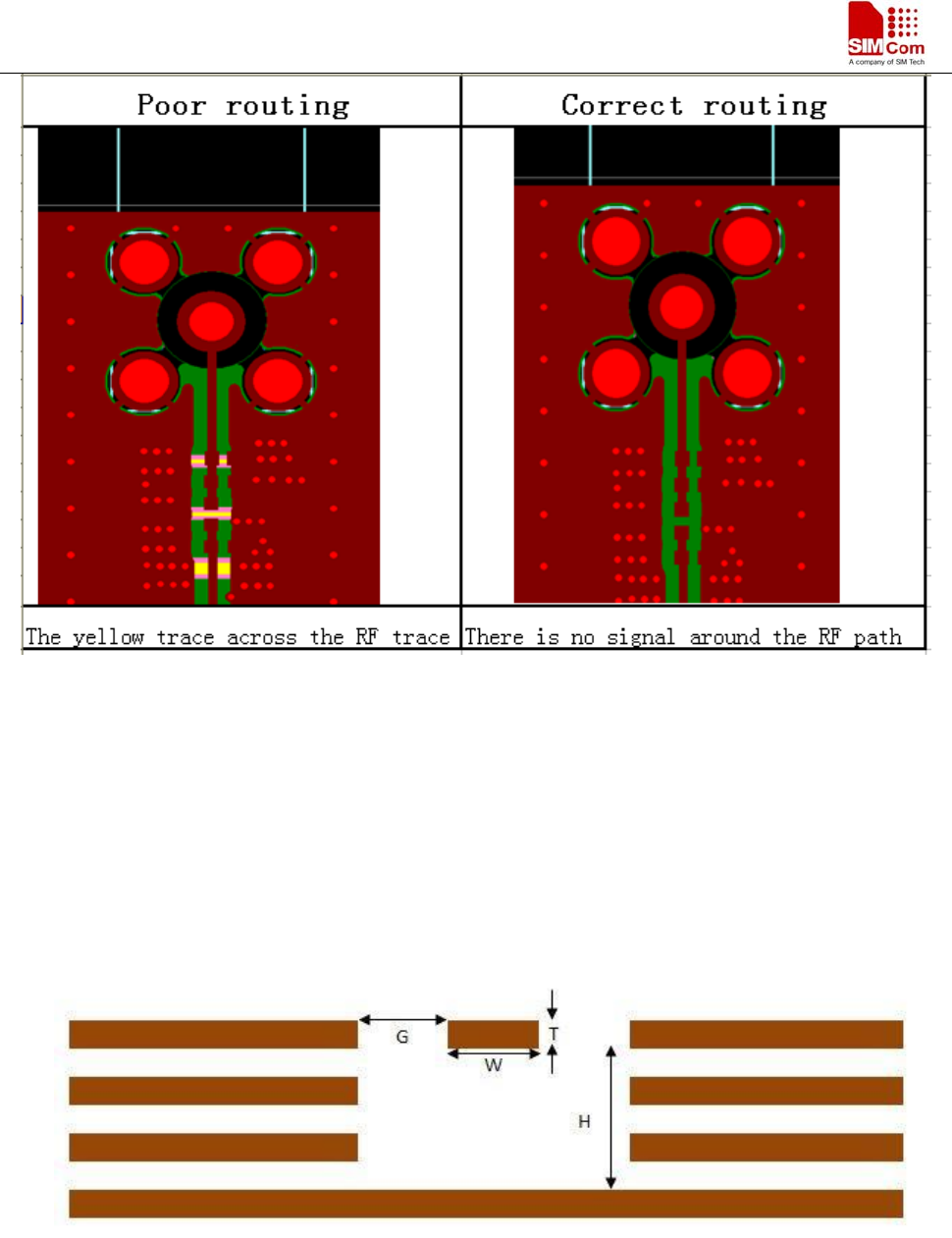
The coplanar clearance (G, below) from the trace to the ground should be at least the trace width (W) and at
least twice the height (H). This reduces the parasitic capacitance, which potentially alters the trace impedance
and increases the losses. Note the figure below shows several internal ground layers cutout, which may not
be necessary for every application.
Figure 7: Coplanar clearance example
6. Regulatory Information
Important notice
Because of the nature of wireless communications, transmission and reception of data can never be guaranteed.
Data may be delayed, corrupted (i.e., have errors) or be total y lost.
SIM900E Document
- 13 -
Although significant delays or losses of data are rare when wireless devices such as the SIMCom modem are used
in a normal manner with a well-constructed network, the SIMCom modem should not be used in situations where
failure to transmit or receive data could result in damage of any kind to the user or any other party, including but
not limited to personal injury, death, or loss of property. SIMCom and its affiliates accept no responsibility for
damages of any kind resulting from delays or errors in data transmitted or received using SIMCom modem, or for
failure of the SIMCom modem to transmit or receive such data.
Safety caution
Marks Requirements
When in a hospital or other health care facility, observe the restrictions about the use of mobiles.
Switch the cellular terminal or mobile off, medical equipment may be sensitive to not operate
normally for RF energy interference.
Switch off the cellular terminal or mobile before boarding an aircraft. Make sure it is switched off.
The operation of wireless appliances in an aircraft is forbidden to prevent interference with
communication systems. Forget to think much of these instructions may lead to the flight safety or
offend against local legal action, or both.
Do not operate the cellular terminal or mobile in the presence of flammable gases or fumes. Switch
off the cellular terminal when you are near petrol stations, fuel depots, chemical plants or where
blasting operations are in progress. Operation of any electrical equipment in potentially explosive
atmospheres can constitute a safety hazard.
Your cellular terminal or mobile receives and transmits radio frequency energy while switched on.
RF interference can occur if it is used close to TV sets, radios, computers or other electric
equipment.
Road safety comes first! Do not use a hand-held cellular terminal or mobile when driving a
vehicle, unless it is securely mounted in a holder for hands free operation. Before making a call
with a hand-held terminal or mobile, park the vehicle.
GSM cellular terminals or mobiles operate over radio frequency signals and cellular networks and
cannot be guaranteed to connect in all conditions, for example no mobile fee or a invalid SIM card.
While you are in this condition and need emergent help, please remember using emergency calls.
In order to make or receive calls, the cellular terminal or mobile must be switched on and in a
service area with adequate cellular signal strength.
Some networks do not allow for emergency call if certain network services or phone features are in
use (e.g. lock functions, fixed dialing etc.). You may have to deactivate those features before you
can make an emergency call.
Also, some networks require that a valid SIM card be properly inserted in the cellular terminal or
mobile.
Important Compliance Information for USA OEM Integrators
The SIM900E modem is granted with a modular approval for mobile applications. Integrators may use the
SIM900E modem in their final products without additional FCC (Industry Canada) certification if they meet the
following conditions. Otherwise, additional FCC approvals must be obtained.
1. At least 20cm separation distance between the antenna and the user’s body must be maintained at all times.
2. To comply with FCC/IC regulations limiting both maximum RF output power and human exposure to RF

SIM900E Document
- 14 -
radiation, the maximum antenna gain including cable loss in a mobile-only exposure condition must not exceed
4.5dBi for GSM850 band and 2.5dBi for GSM PCS band.
3. SIM900E modem and the antenna must not be co-located or operating in conjunction with any other
transmitter or antenna within a host device.
4. A label must be affixed to the outside of the end product into which the SIM900E modem is incorporated,
with a statement similar to the following:
a. For SIM900E: This device contains FCC ID: UDV-SIM900E
A user manual with the end product must clearly indicate the operating requirements and conditions that must be
observed to ensure compliance with current FCC RF exposure guidelines. The end product with an embedded
SIM900E modem may also need to pass the FCC Part 15 unintentional emission testing requirements and be
properly authorized.
Note: If this module is intended for use in a portable device, you are responsible for separate approval to satisfy
the SAR requirements of FCC Part 2.1093