Simoco EMEA SDB670TU01 25W D.C. TU Band SDB670 User Manual manual
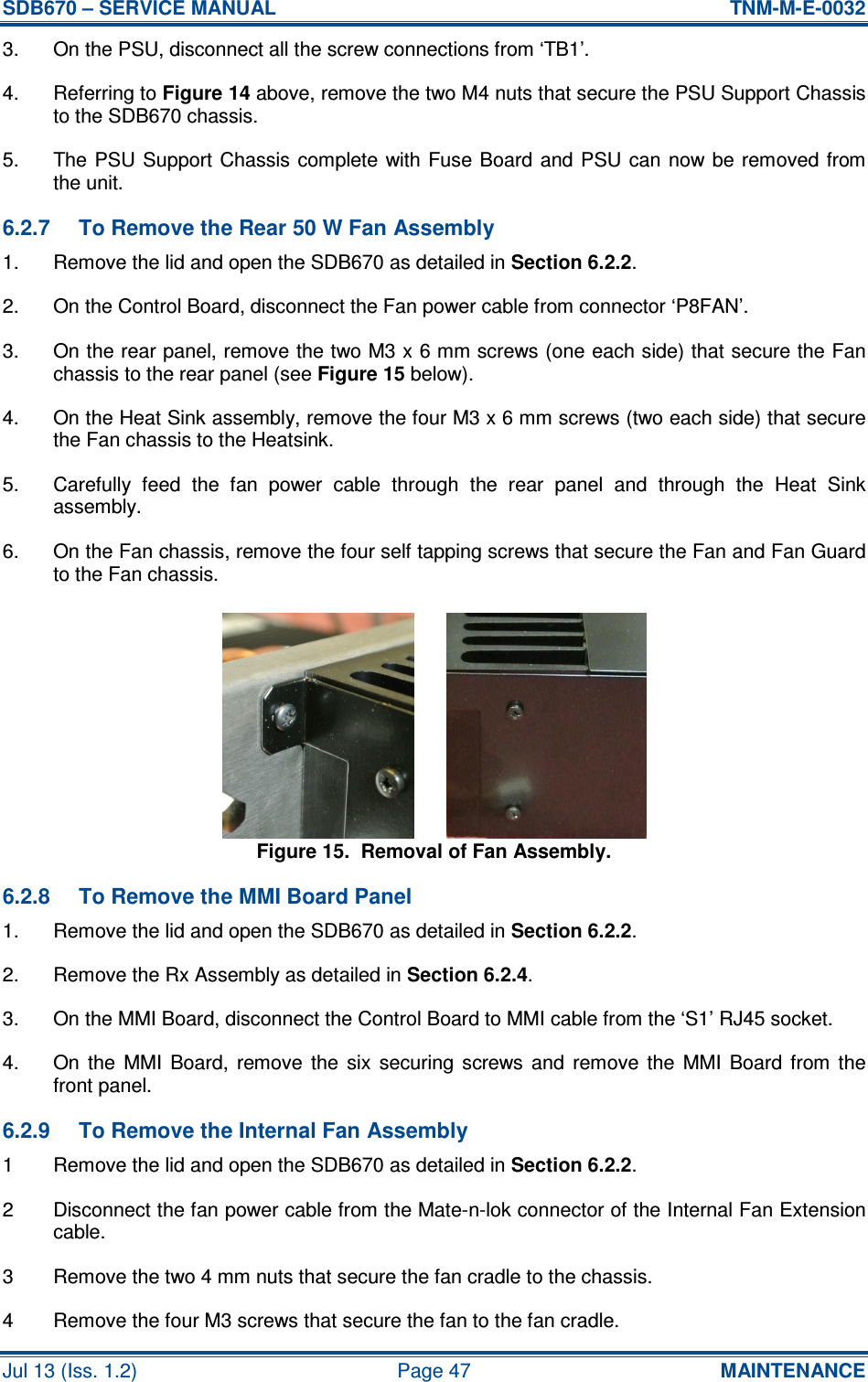
Simoco EMEA Ltd 25W D.C. TU Band SDB670 manual
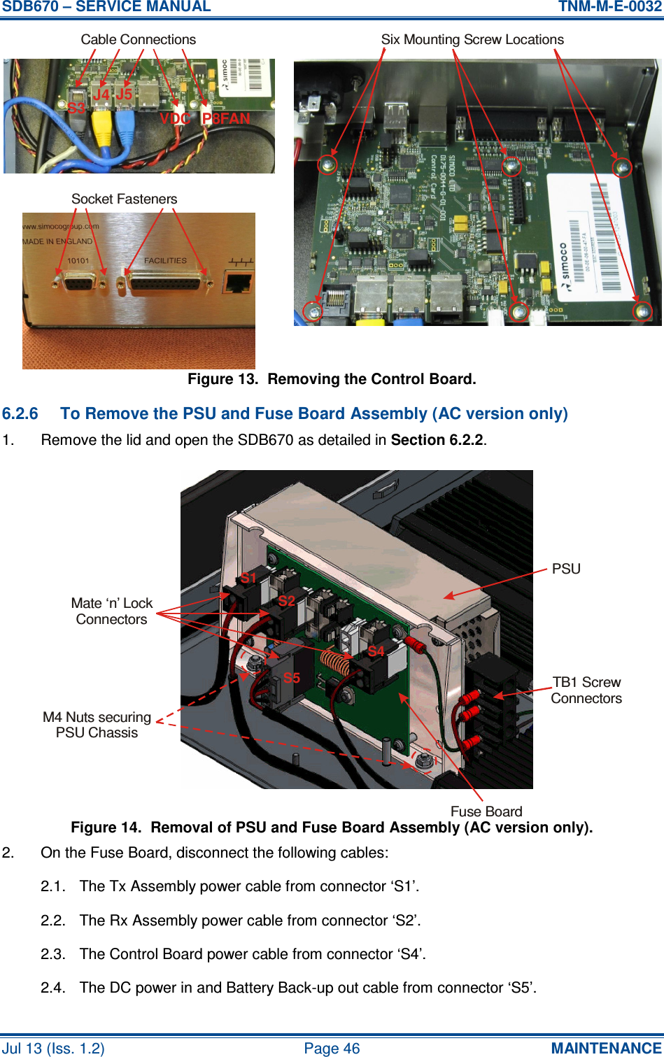
UserManual.wiki
>
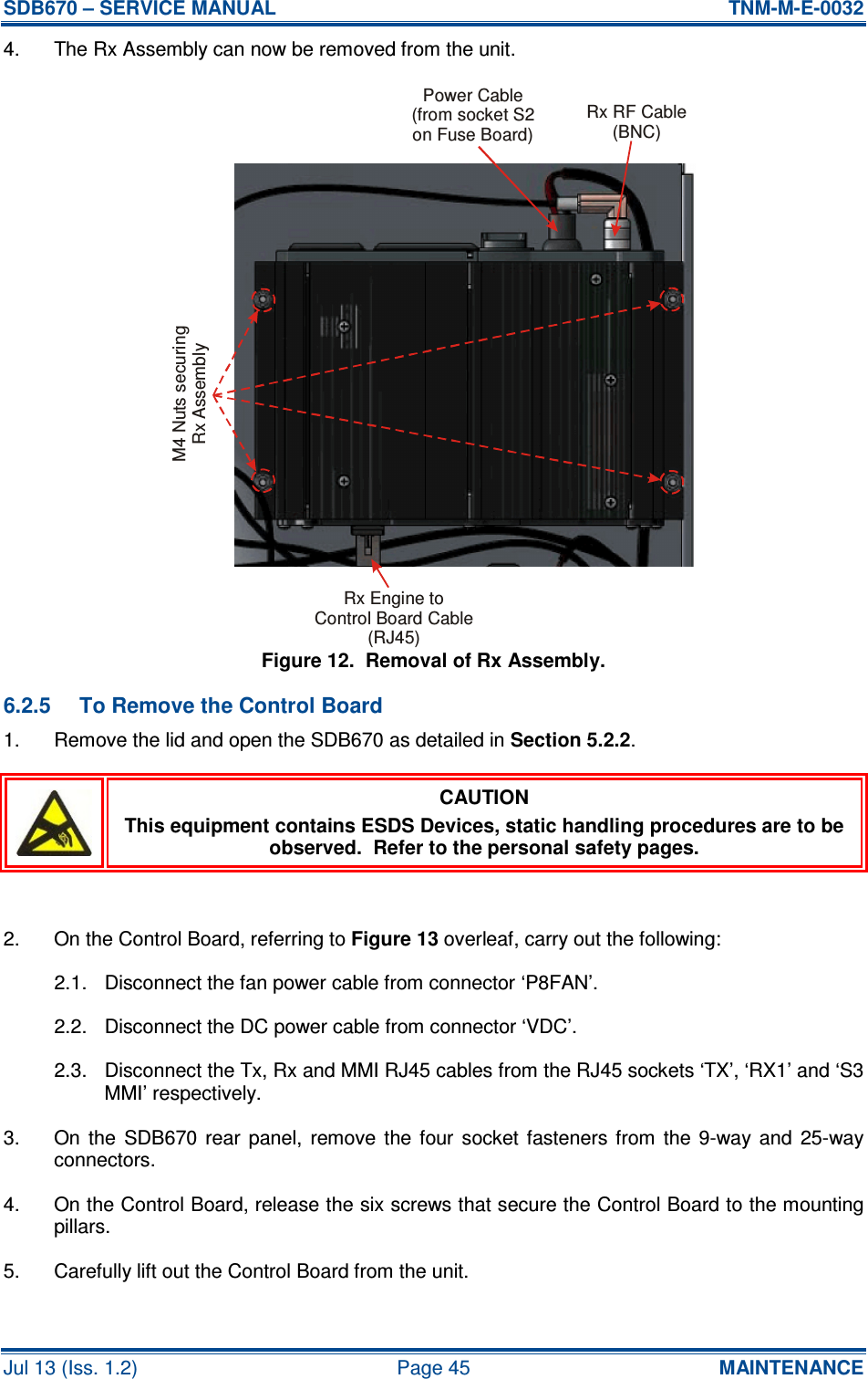
Simoco EMEA
>
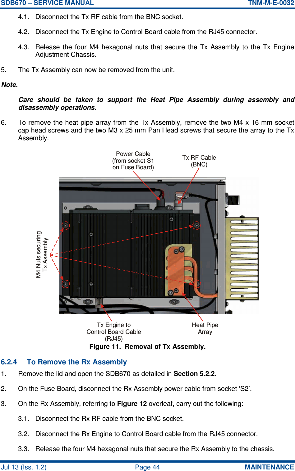
SDB670TU01 User Manual
manual
Navigation menu
Upload a User Manual
Namespaces
Wiki Guide
HTML
PDF
Info
Views
User Manual
Discussion / Help
Navigation

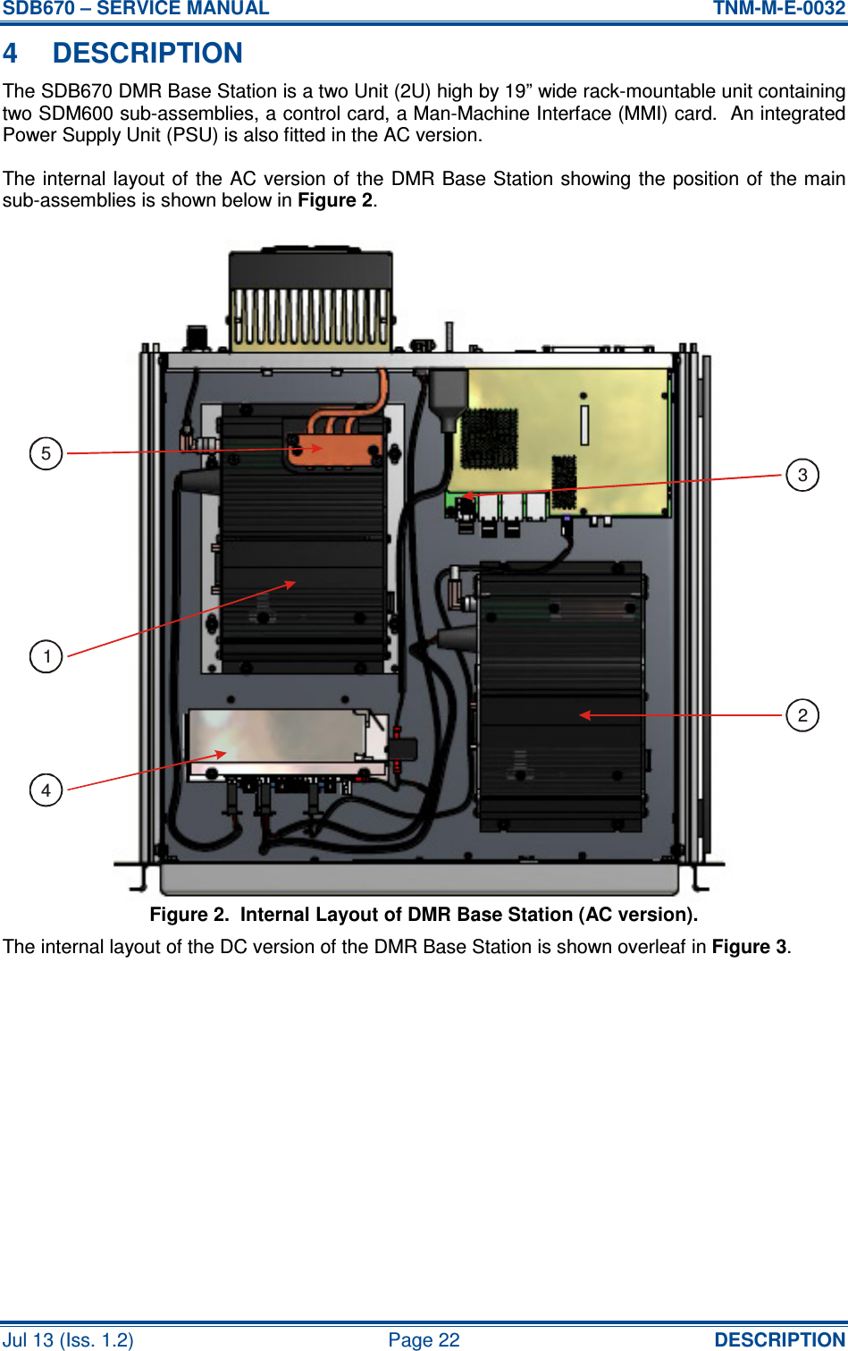
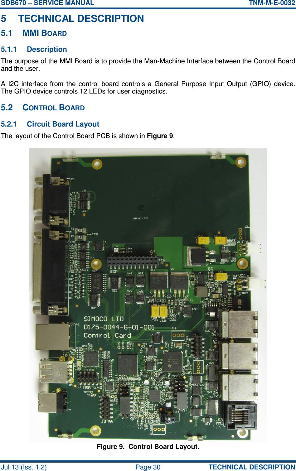
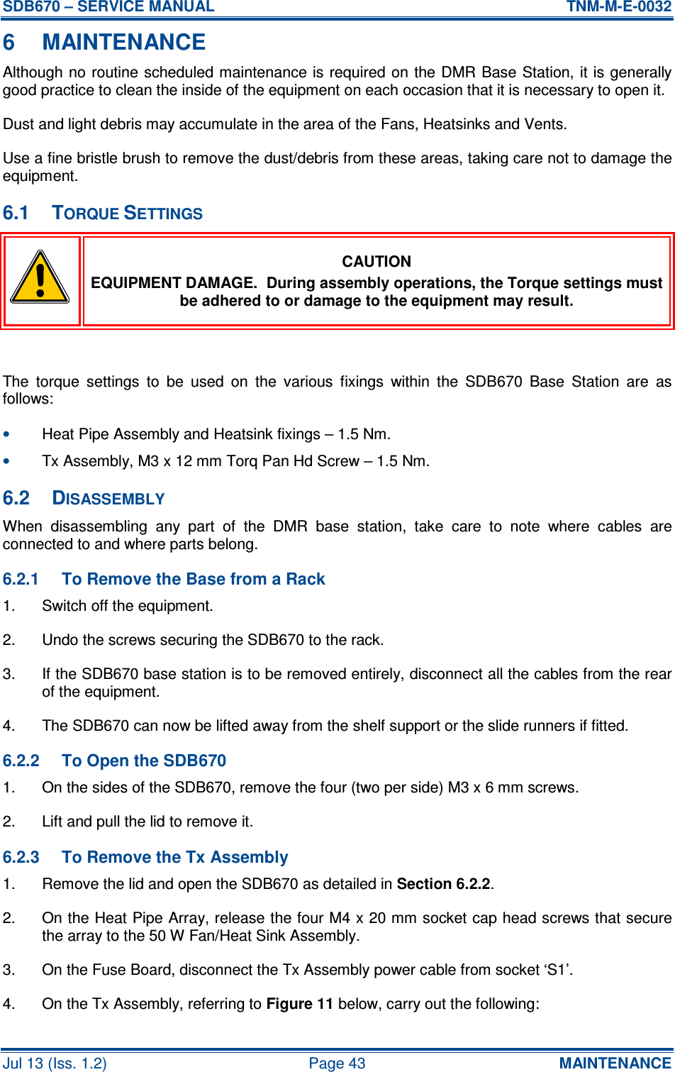
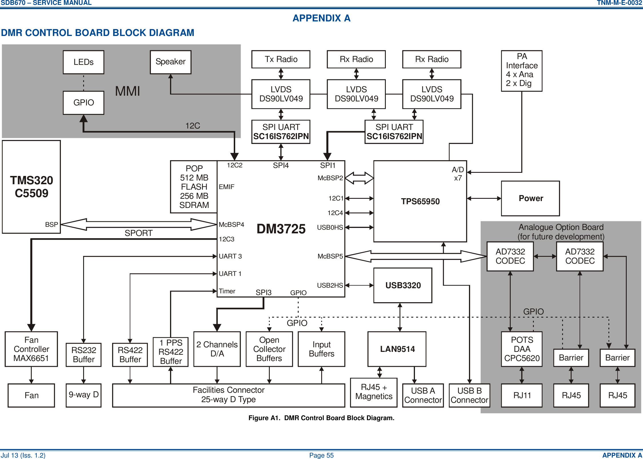
![SDB670 – SERVICE MANUAL TNM-M-E-0032 Jul 13 (Iss. 1.2) Page 32 TECHNICAL DESCRIPTION Analogue Inputs The PMIC provides multiple analogue inputs which are currently used to provide voltage monitoring of the unregulated supply. GPS Input The facilities connector provides an RS422 serial connection with a primary purpose of connecting a GPS receiver to provide an accurate time stamp. An RS422 input is also provided for connection of the 1PPS output from a GPS Rx to provide a very accurate reference clock to tune the internal oscillator. External Power The control card provides the supply voltage at up to 1 A on the facilities connector. RS232 Serial Interface (DB9) The rear of the control card contains a standard 9-way serial connection in order that a straight through cable may be used to provide debug and control data. Expansion Header An expansion header provides the necessary signals to support a multitude of future expansion boards. 5.3 TRANSMITTER AND RECEIVER MODULES 5.3.1 Control Refer to Figure 10 (page 42) and Figures 2 and 3 in TNM-S-E-0005, SDM600 Series – Issue 4 Circuit Diagrams [2]. DSP and FPGA The SDM600 transceiver operates under the control of a DSP (U203) and Field Programmable Gate Array (FPGA) (U300) combination that, together with a number of other dedicated devices, perform all the operational and processing functions required by the radio, the software for which is contained in flash memory. The FPGA contains an internal embedded processor core and provides the majority of radio functionality, including demodulation, while the DSP provides most of the complex filter and timing functions, a 57.6 MHz clock to the FPGA and ADC conversion. Both the DSP and FPGA have internal Random Access Memory (RAM) for rapid code execution. In addition, the FPGA utilizes external RAM contained in Cellular RAM U304 for increased capacity. The FPGA in conjunction with the DSP provides the following functions: • Channel set-up of all operating frequencies. • Modulation processing and filtering. • De-modulation processing and filtering. • Tx power output. • Modulation equalisation adjustment. • Rx front-end tuning. • Serial communications with Alignment Tool and options including LVDS for microphone and control head. • Modem functionality for data modulation. • All DMR/CTCSS/DCS generation and decoding.](https://usermanual.wiki/Simoco-EMEA/SDB670TU01/User-Guide-2084039-Page-32.png)
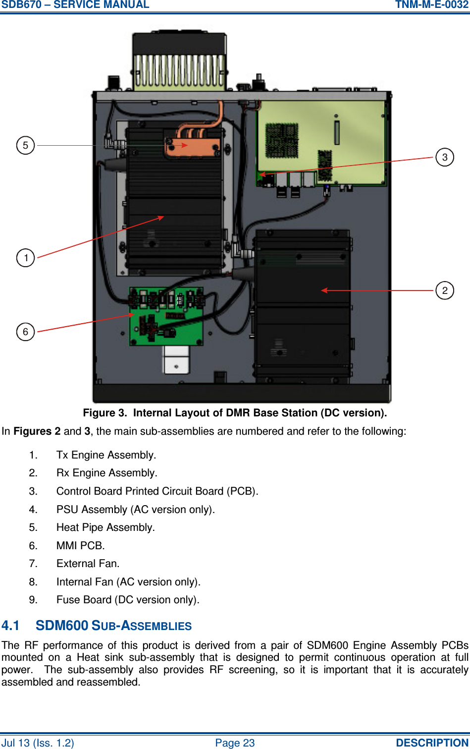
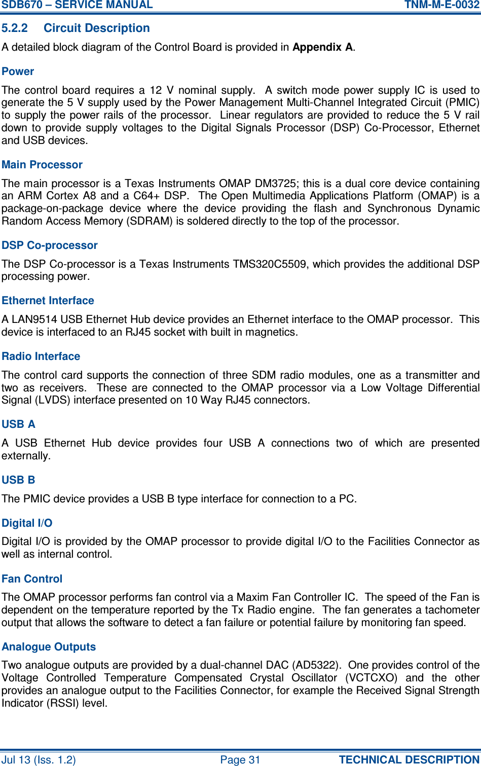
![SDB670 – SERVICE MANUAL TNM-M-E-0032 Jul 13 (Iss. 1.2) Page 34 TECHNICAL DESCRIPTION downloads the DSP and FPGA software from Flash Memory to their internal RAMs for faster program execution and access to data. All software, except for the customer configuration, is loaded by the factory into the Flash Memory and can be updated via the SDM600/SDP600 Code Loader connected to external interface connector S3. DSP software comprises Boot code and Application code, while FPGA code comprises FPGA code and MCP code. High-level software comprising Operational Code and Customer Configuration is loaded at distribution centres and is loaded via the SDM600/SDP600 Field Personality Programmer (FPP). 5.3.2 Receiver Refer to Figure 10 (page 42) and Figures 7 and 11 in TNM-S-E-0005, SDM600 Series – Issue 4 Circuit Diagrams [2]. Front End Filters and RF Amplifier The Rx input signal from the antenna passes through the harmonic filter and antenna switch. With the mobile in receive mode, diodes D500, D5502 and D503 in the antenna switch are reverse biased allowing the Rx input signal to be coupled through to the Rx front-end with minimal loss. The overall insertion loss of the harmonic filter and switch is approximately 0.8 dB. A noise blanker is also fitted to E0 band radios. The noise blanker samples the received signal and gates the 45 MHz signal in the Intermediate Frequency (IF) stage in the event that high level noise transients are received. Due to inherent time delays in the bandpass filters prior to the blanking gate, gating synchronisation occurs before the transients can adversely affect the following stages. Varactor-tuned bandpass filters at the input and output of the RF amplifier provide Rx front-end selectivity. Varactor tuning voltages are derived from the alignment data stored in the radio. The DSP processes this data to optimise front end tuning relative to the programmed channel frequencies, which may be changed at any time without re-aligning the radio. To achieve the required varactor tuning range, an arrangement of positive and negative bias power supplies is used to provide a total bias across the varactors of up to 14.0 VDC. A fixed 1.6 V positive bias derived from the 3.2 V supply and voltage divider R438/R439 is applied to the cathodes of the varactor diodes. The negative bias supplies are derived from –12 V and controlled by the FPGA, which outputs PWM for the four front-end tuning voltages RX-TUNE1 to 4, for the particular channel frequency selected. The PWM signal is dependent on channel frequency and tuning and passes through level shifting transistors Q403 to Q410 where it is converted to a negative voltage in the range –0.5 V to –11.5 V. The –12 V rail of the level translators is generated by U908A/B/F with D912 to D915 providing the required voltage multiplication. The RF amplifier stage comprises a low noise transistor amplifier Q402, which is compensated to maintain good linearity and low noise matching, and Q400/Q401 provide it with a constant current source. This provides excellent intermodulation and blocking performance across the full operating range. The overall gain of the front-end is typically 14 dB for all bands. D412 provides protection for Q402 from high level signals. Mixer and IF Section The output of the last front-end bandpass filter is coupled into a double balanced mixer comprising T471/D470/T472, which converts the RF signal to an IF frequency of 45 MHz. The local oscillator injection level from the Voltage Controlled Oscillator (VCO) is typically +7 dBm at TP414 with low side injection used for UHF bands and high side for frequency bands less than 400 MHz. Following the mixer is crystal filter Z400, its matching networks and IF amplifier Q419. The IF amplifier provides approximately 20 dB of gain, and drives an AGC circuit comprising D413/D414. The purpose of the AGC circuit is to linearise the Rx gain across the band as well as limiting very high level signals that could reduce the Rx performance. The AGC is set via RX-AGC during radio alignment and is controlled via a PWM output from the FPGA. The gain of Q419 can also be](https://usermanual.wiki/Simoco-EMEA/SDB670TU01/User-Guide-2084039-Page-34.png)
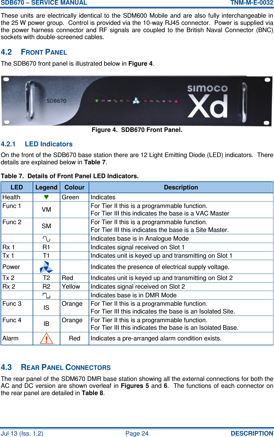
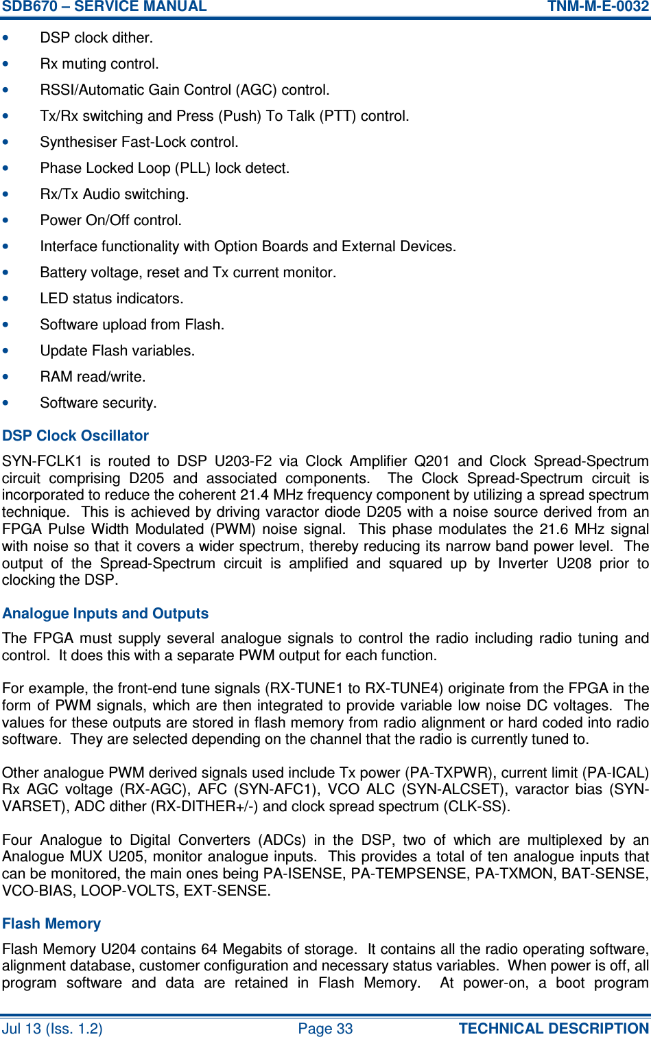
![SDB670 – SERVICE MANUAL TNM-M-E-0032 Jul 13 (Iss. 1.2) Page 35 TECHNICAL DESCRIPTION reduced by approximately 20 dB in a single step when D415/D416 are turned on by the FPGA via RX-GAIN. The output of the AGC circuit contains a matching network for the following crystal filter Z401, which in turn is matched to a dual current amplifier U402. The crystal filters provide part of the required selectivity for rejection of close in unwanted signals. The current amplifier provides an unbalanced to balanced conversion as well as providing a low source impedance suitable for driving the following DAC U401. The filter comprising L485a/L486a and associated components provides correct matching to the IF ADC. IF Analogue to Digital Convertor The 45 MHz balanced output from the IF stages is fed to U401 pins 1 and 2 where it is directly clocked in via a 21.6 MHz clock at pin 9. This converts the 45 MHz analogue signal to 12 bit digital outputs ADC-0 to ADC-D11. In addition, dither inputs are also provided in parallel with the IF input via shaping filter L490/L491 and associated components. The dither inputs are derived from the FPGA as 48 kHz triangular waveforms at a level such that improved resolution of the least significant ADC bit can be obtained, effectively resulting in a reduction of at least 40 dB to the measured noise floor, thereby enabling the measurement of a much lower level of IF signal. Suitable high frequency roll-off is provided on all the digital outputs to minimize noise. In addition, a 1.5 V reference voltage is derived from U401-31 which is used for biasing its analogue inputs and also to provide low impedance current limited source voltages 1V5-S and 1V5-REF via U400. The 12 bit digital outputs running at a 21.6 MHz sample rate are fed to the FPGA U300 where they are processed to form I/Q quadrature signals running at a 96 kHz sample rate. This is then fed through a series of digital filters to provide the final stage of adjacent channel filtering, after which it is fed to the DSP U203 via the EMIF bus. 5.3.3 Transmitter Refer to Figure 10 (page 42) and Figures 8 and 12 in TNM-S-E-0005, SDM600 Series – Issue 4 Circuit Diagrams [2]. Drivers and PA Stages The VCO provides approximately 7 dBm output that is switched to the Tx Buffers via T/R switch comprising D700 and D701. Tx buffers Q501 and Q502 increase the VCO level to provide approximately 17 dBm of drive power to the Tx driver Q500. The Tx driver stage then typically provides 16 dBm of drive to the PA module. Inter-stage attenuator networks are provided between all amplifier stages to provide a high degree of isolation of the VCO from the Tx output. PA module U505 utilises three Metal Oxide Semiconductor Field Effect Transistor (MOSFET) stages (UHF) and two MOSFET stages (VHF) to achieve the required RF output power up to a level of +44 dBm (25 Watts). The gain of the PA module is controlled by the power control loop to ensure that Tx output power remains within defined limits over supply voltage and temperature extremes. Note. Care should be taken during servicing for low output power. If the drive power is lost, the power control voltage will go high, which may cause the current or power into the PA to exceed its specification. Therefore, the power supply current should be monitored at all times and preset to as low as required. The radio has additional inbuilt safeguards, but these should not be relied on.](https://usermanual.wiki/Simoco-EMEA/SDB670TU01/User-Guide-2084039-Page-35.png)
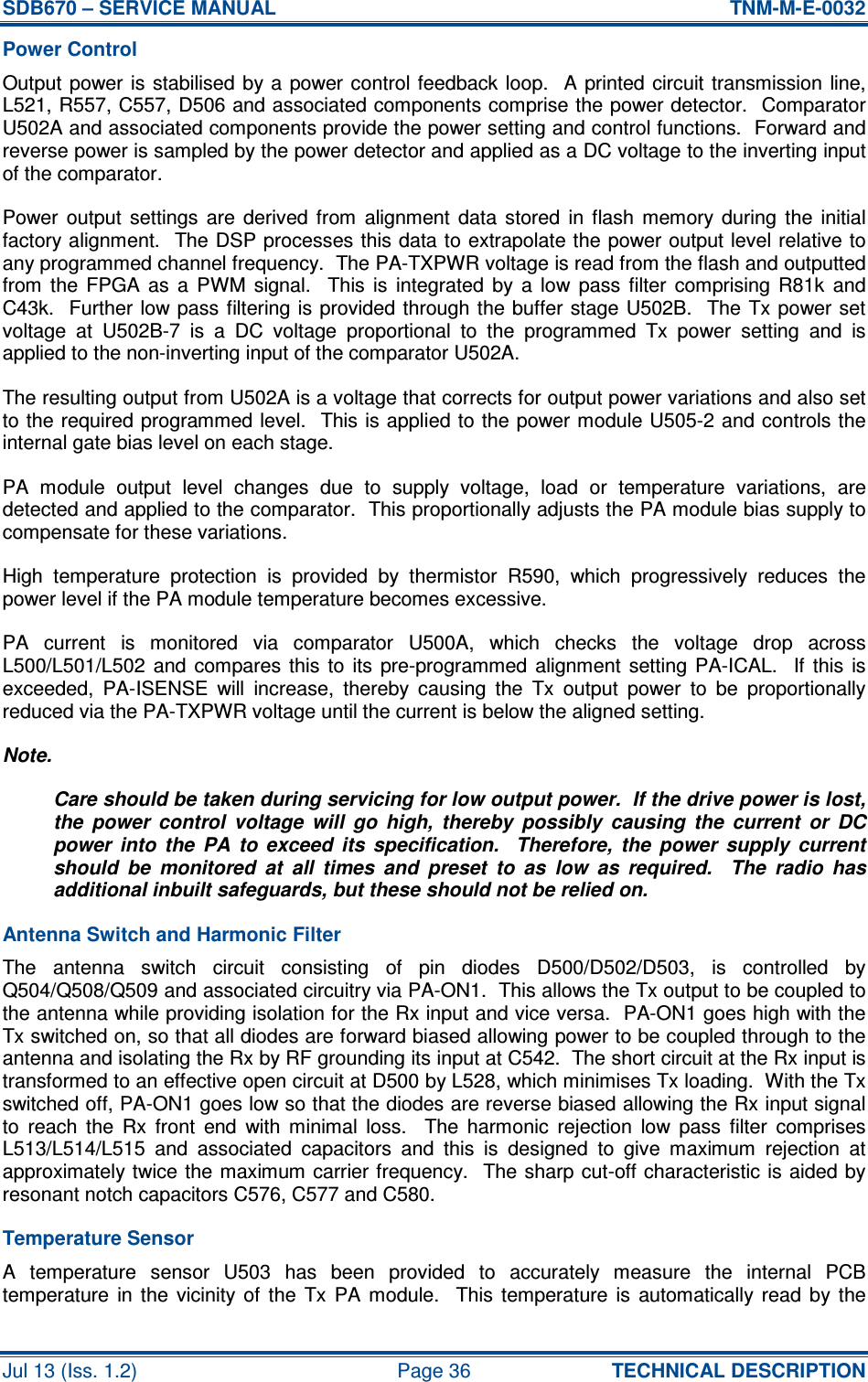
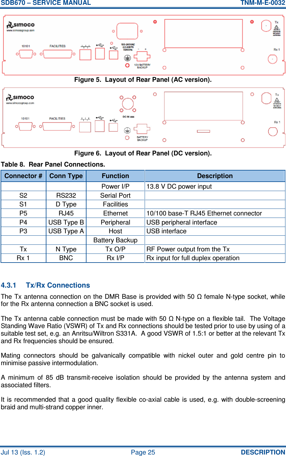
![SDB670 – SERVICE MANUAL TNM-M-E-0032 Jul 13 (Iss. 1.2) Page 37 TECHNICAL DESCRIPTION Alignment Tool to measure the actual operating temperature and can also be used for advanced control functions. 5.3.4 Frequency Synthesiser General Refer to Figure 10 (page 42) and Figures 9, 10, 13 and 14 in TNM-S-E-0005, SDM600 Series – Issue 4 Circuit Diagrams [2]. The frequency synthesiser consists of one VCO each for the Tx and Rx, loop filter, varactor negative bias generator, reference oscillator, a dual PLL U701, VCO buffers and PLL feedback buffer. Fractional PLL The Fractional PLL device contains two prescalers, programmable dividers and phase comparators to provide a main and auxiliary PLL. The main PLL of U701 controls the frequency of the Tx/Rx VCOs via Charge Pump output CPRF at pin 1 via the Loop Filter. This voltage is set to a nominal 1.6 V that provides a suitable operating point for the VCO varactor diodes. This voltage will be maintained for any frequency but may vary slightly with temperature. VCO feedback to pin 4 is provided via Feedback Buffer Q710 and associated circuitry. The auxiliary PLL is not used in this application. The PLL operation involves the division of the 95.04 MHz reference frequency to a preset comparator frequency of 1760 kHz (Rfr1=54) or 1728 kHz (Rfr2=55) by internal dividers. The VCO frequency is sampled and divided down to the same comparison frequency after which it is phase compared to the comparator reference. The fractional feature of this PLL enables very fine increments of the channel frequency such that any customer requirement can be fulfilled. Any error produces an offset to the Charge Pump output voltage, which is then used to correct the VCO frequency. A valid lock detect output is derived from PLL pin 12 and is sampled by the FPGA. During transmit, if an unlocked signal is detected, the radio will switch back to receive mode. An unlocked signal in receive mode will cause the radio to beep. The Feedback Buffer circuit is provided in the feedback path to provide VCO isolation and correct input level to the PLL. Negative Bias Generator and Loop Filter A negative varactor bias supply similar to the front-end varactor arrangement has been used to achieve the required broadband tuning range of the VCOs. This voltage is filtered by R706 and C717 to provide a very clean output to the VCOs and it can vary between –0.5 V and –16 V. It is controlled by SYN-VARSET and is derived from another PWM output from the FPGA. This voltage is translated to a negative voltage by the circuit comprising Q701 to Q704. The resulting low noise voltage VAR-BIAS is applied to the anode side of the VCO varactor tuning diodes as a negative bias voltage. The –16 V rail of this supply is generated by U908A/B/F with D912 to D915 providing the voltage multiplication needed to achieve –16 V. The Loop Filter, comprising R719, R719b, R721, C722 to C725a, C731d and C732, is placed in series with CPP-RF and U701-1 and connected to VAR-BIAS as its reference. The purpose of the Loop Filter is to remove Charge Pump reference components and other PLL generated noise. However, this requirement conflicts with the extremely fast switching times required for DMR operation. As a result, a quad analogue gate U700 has been added. This switches in fast time constant values across the Loop Filter components to rapidly stabilise the CPP-RF output prior to transmission or reception. Timing for these gates is controlled by the FPGA via SYN-FAST1 and SYN-FAST2. Reference Oscillator Temperature Controlled Crystal Oscillator (TCXO) U702 determines the overall frequency stability and frequency setting of the radio. The frequency setting is achieved by adjusting its ADJ voltage SYN-AFC1 with the Alignment Tool. In addition, the ADJ input can be used in a frequency control loop with the demodulated I and Q signals to provide Rx Automatic Frequency Control (AFC).](https://usermanual.wiki/Simoco-EMEA/SDB670TU01/User-Guide-2084039-Page-37.png)
![SDB670 – SERVICE MANUAL TNM-M-E-0032 Jul 13 (Iss. 1.2) Page 38 TECHNICAL DESCRIPTION U702 operates at 21.6 MHz and is specified at ±0.5 ppm frequency stability over the temperature range –30 °C to +85 °C. Its output drives Clock Synthesiser U720 to provide two digital 21.6 MHz outputs and a 95.04 MHz output. The 95.04 MHz output is used as the reference frequency for the PLL as described above. The 21.6 MHz output SYN-ACLK is used as the clock for the Rx ADC U401 and the other 21.6 MHz output SYN-DCLK1 goes via Schmitt Trigger U307 to provide SYN-FCLK1 to clock the FPGA and also the DSP. VCO’s The Tx and Rx VCO’s use low noise transistors Q602 (Rx), Q604 (Tx) and associated parts to generate the signals for the required band coverage. Electronic tuning is provided by varactor diodes D604 to D615 where fitted with their control voltage CPP-RF derived from the Loop Filter and PLL. A Negative Bias Generator is used to apply an adjustable negative bias to the varactor anodes to extend their tuning range. VCO switching and timing is controlled by the DSP/FPGA via the 5V-RX and 5V-TX power supplies and applied through switches Q607 (Rx) and Q608 (Tx). VCO buffer Q605/Q606 isolates the VCO from load variations in following circuits and active power supply filter Q600 minimises supply related noise. A PLL feedback signal is sampled from the VCO buffer output via buffer Q710. The output from the VCO Buffers is passed through Tx/Rx switch D700/D701, which switches it between either to the Mixer input or Tx Buffer. This switch is controlled by the 5V-RX supply. In addition, each VCO includes an RF negative feedback network (ALC) to set their operation levels for optimum noise reduction. This is achieved via diodes D616 to D619 that rectify the RF signal. This is filtered and applied to input pins on op-amp U600, which provides amplified correction voltages to the base bias of Q602 and Q604. This circuit also contains a means of presetting and monitoring of the operating current via VCO-BIAS and SYN-ALCSET. The SYN-ALCSET value is factory preset and stored in Flash. 5.3.5 Audio Processing Refer to Figure 10 (page 42) and Figure 5 in TNM-S-E-0005, SDM600 Series – Issue 4 Circuit Diagrams [2]. Receiver Audio The baseband quadrature signal sent to the DSP U203 is converted into a single digital data input CD-DIN to the Coder-Decoder (CODEC) U803, which in turn converts it into an analogue signal after further processing. All Rx audio processing and filtering functions are performed by the CODEC under the control of the DSP. These include de-emphasis, mute noise processing, mute control and volume control for narrow and wideband operation. A CODEC DAC then converts the fully processed signal to an analogue audio signal. Independent processing can be achieved on four separate outputs C-OUT1, C-OUT2, C-OUT3 and C-OUT4, which enables great flexibility to suit customer requirements. C-OUT3 normally provides volume controlled, de-emphasised audio to the audio PA U808 via differential amplifier U804A. With a normal radio FPP configuration, the maximum sinusoidal output is limited to 4 VRMS across the 4 Ω speaker. However, when more power is required, it is possible to achieve up to 16 W into a suitable 4 Ω speaker. In addition to the CODEC mute control, the audio PA is also muted on and off via inverter Q800 and CD-SPKRON derived from the FPGA. The other CODEC outputs C-OUT2, C-OUT3 and C-OUT4 can provide any combination of audio characteristics including muted, unmuted, de-emphasised, flat and volume dependency. All CODEC outputs are fed to analogue gate U806 via differential amplifiers U804 and U805. This enables switching flexibility to the radio connectors S1-4 (LINE-OUT1), S3-1 (LINE-OUT3) and S5-18 (LINE-OUT2).](https://usermanual.wiki/Simoco-EMEA/SDB670TU01/User-Guide-2084039-Page-38.png)
![SDB670 – SERVICE MANUAL TNM-M-E-0032 Jul 13 (Iss. 1.2) Page 39 TECHNICAL DESCRIPTION U805A and U805B are set up as differential constant current amplifiers with 600 Ω source impedances. U804A and U804B are differential voltage amplifiers with LINE-OUT source impedances of approximately 600 Ω and 40 Ω respectively. An optional CODEC U800 can be provided to provide more complex functionality but is normally not fitted. Transmitter Audio The microphone audio input signal is applied to the microphone input at S1-8 and is derived from an external microphone unit with an applied nominal level of 40 mVRMS. This is then routed to CODEC U803-35 as MIC-AUDIO where it is limited to approximately 800 mVp-p by D801. Microphone bias, if required, is derived from U803-36, which can apply a pre-programmed bias voltage to the microphone. Alternate modulation inputs from connectors S3-4 (LINE-IN2), S5-19 (LINE-IN4), S5-14 (LINE-IN5) can also be provided. CODEC U803 provides input switching of the audio paths after which they are fed to one of two CODEC ADCs. The output of these is routed to the DSP via CD-OUT. All pre-emphasis, filtering, compression and limiting processes for narrow and wideband operation are carried out in the DSP. This processed Tx audio/data is then fed to a Modulation Equaliser that takes equalisation values stored in flash after radio alignment. It applies these values to the Tx data and then directly programs these into PLL U701 via its SYN-PLL-DATA/CLK/STB bus as new frequency data values resulting in frequency modulation of the VCO. The purpose of the Modulation Equaliser is to correct for frequency response variations caused by the VCO loop filter resulting in a flat frequency response from 0 Hz up to the maximum modulation frequency. 5.3.6 Power Supplies Refer to Figure 10 (page 42) and Figures 4 and 6 in TNM-S-E-0005, SDM600 Series – Issue 4 Circuit Diagrams [2]. Power On/Off Function The radio ON/OFF function can be achieved in two ways as follows: (a). Analogue control via Q902, Q922 and Q901. In this case a momentary low voltage pulse from the control unit or microphone handset PWR ON button briefly turns on Q902/Q922/Q901. In this time, the radio powers up and the DSP samples the PWR_DET line after Boot Code has loaded. If this is high, it writes this status to flash, sets PWR-INH low and gets the FPGA to set its PWR-OFF line high. This latches the radio on and the radio remains powered up. If the DSP sees that the PWR-DET is low, it will check the ON/OFF status in flash. If this corresponds to OFF, the DSP will power down the radio by setting PWR-INH high. If the ON/OFF flash status corresponds to ON, the DSP sets PWR-INH low. The FPGA will also read the ON/OFF flash status and will set its PWR-OFF line high so that the radio will remain on. The Power-off operation requires the ON/OFF button to be pressed for more than 2 seconds. If the ON/OFF button is sensed going low for approximately two seconds by the DSP via the PWR_DET line, the DSP will save radio settings to flash including the OFF status. It will then set the PWR-INH line high, thereby turning Q901 and hence the radio off. (b). Digital control via an external device. This is necessary when multiple devices are connected. It enables the radio to determine which devices are connected and which one has master control. When the ON/OFF button is pressed on any device, the radio will turn everything on as described above and a microprocessor in any external device will note this and send and serial ID message to the radio. After everything has been turned on, pressing the ON/OFF button on the master will send a serial command to the radio to turn everything](https://usermanual.wiki/Simoco-EMEA/SDB670TU01/User-Guide-2084039-Page-39.png)