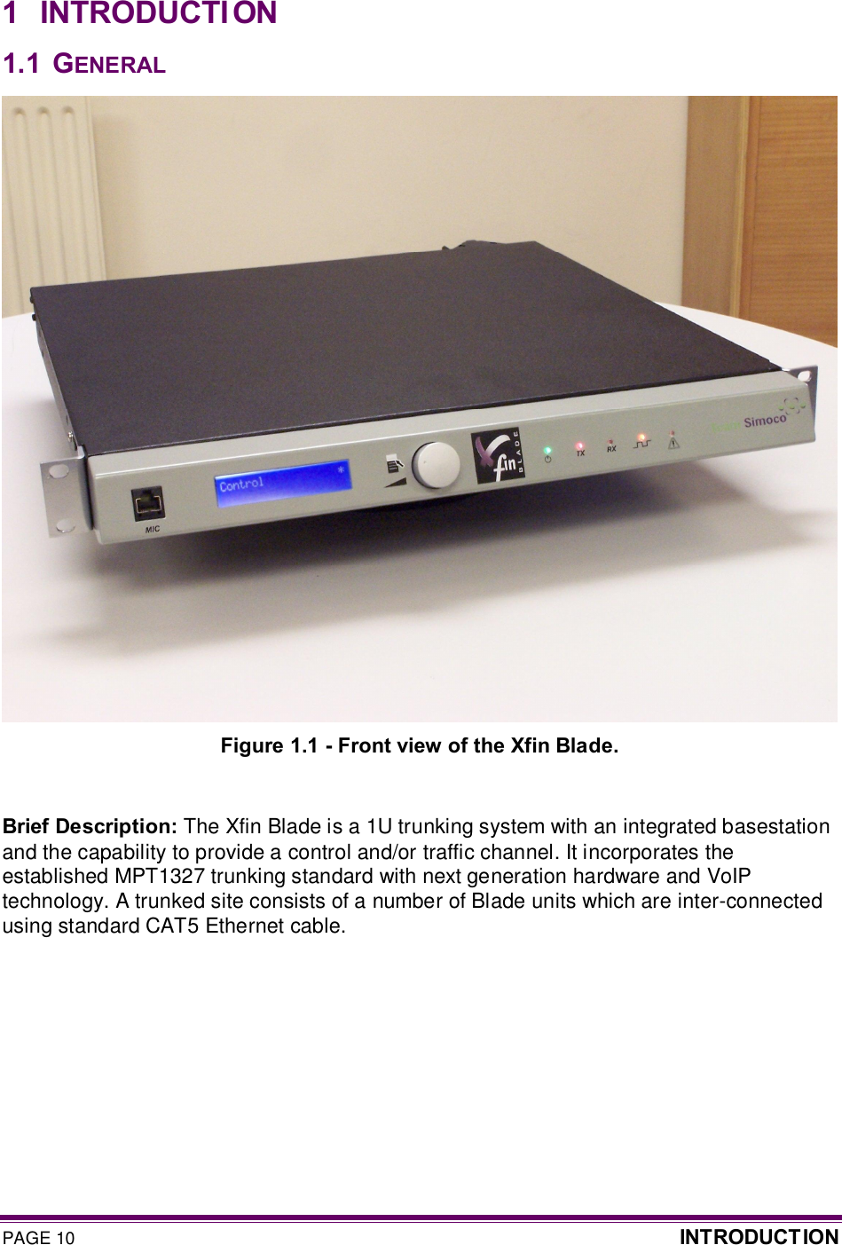
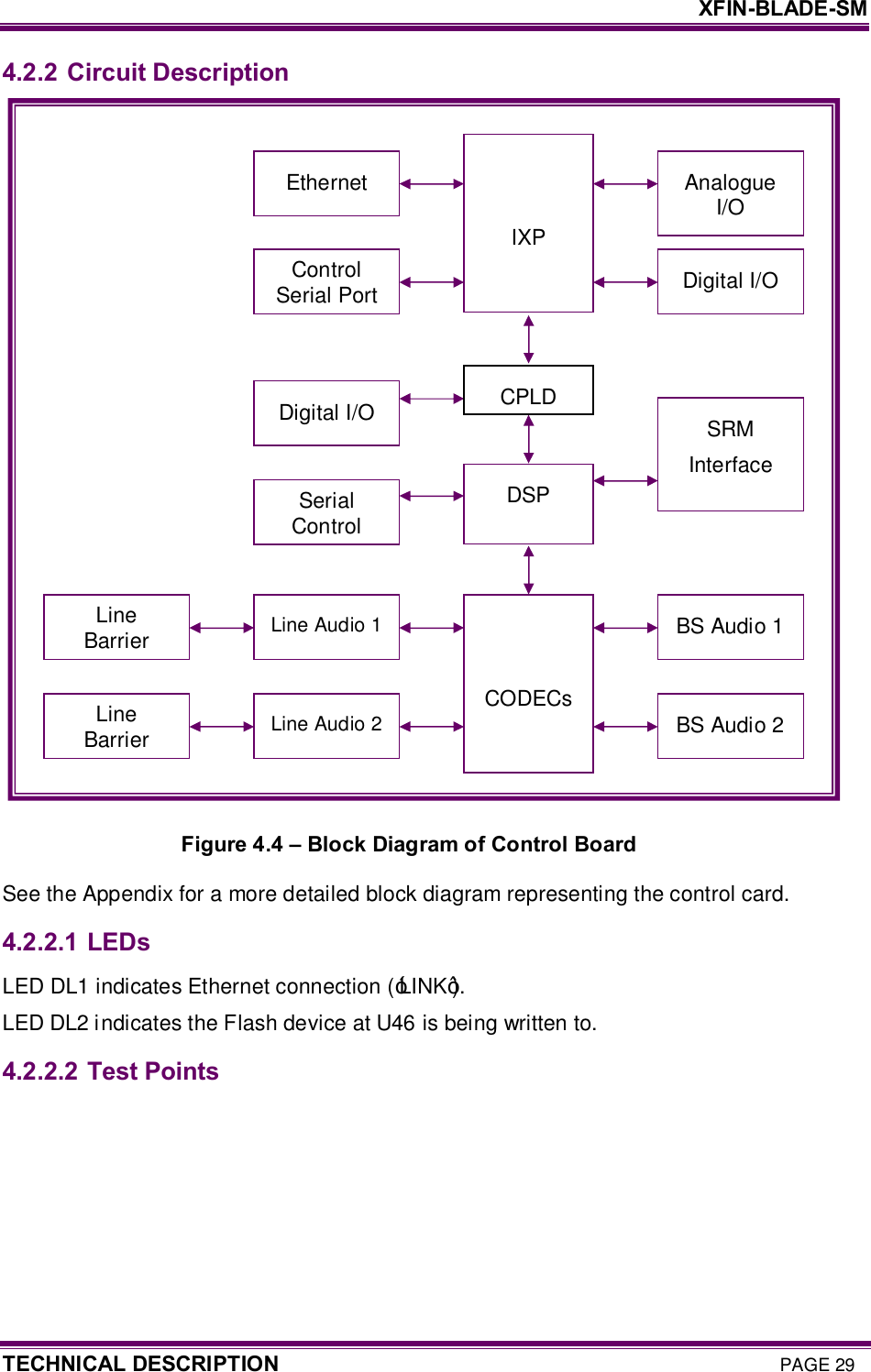
Simoco EMEA XFINBLATU UHF TRUNKING LANDMOBILE BASE STATION User Manual USERS MANUAL
Simoco EMEA Ltd UHF TRUNKING LANDMOBILE BASE STATION USERS MANUAL
UserManual.wiki
>
Simoco EMEA
>
XFINBLATU User Manual
>
USERS MANUAL
Contents
1.
USERS MANUAL
2.
User and Service Manual
3.
Users Manual
USERS MANUAL
Navigation menu
Upload a User Manual
Namespaces
Wiki Guide
HTML
PDF
Info
Views
User Manual
Discussion / Help
Navigation


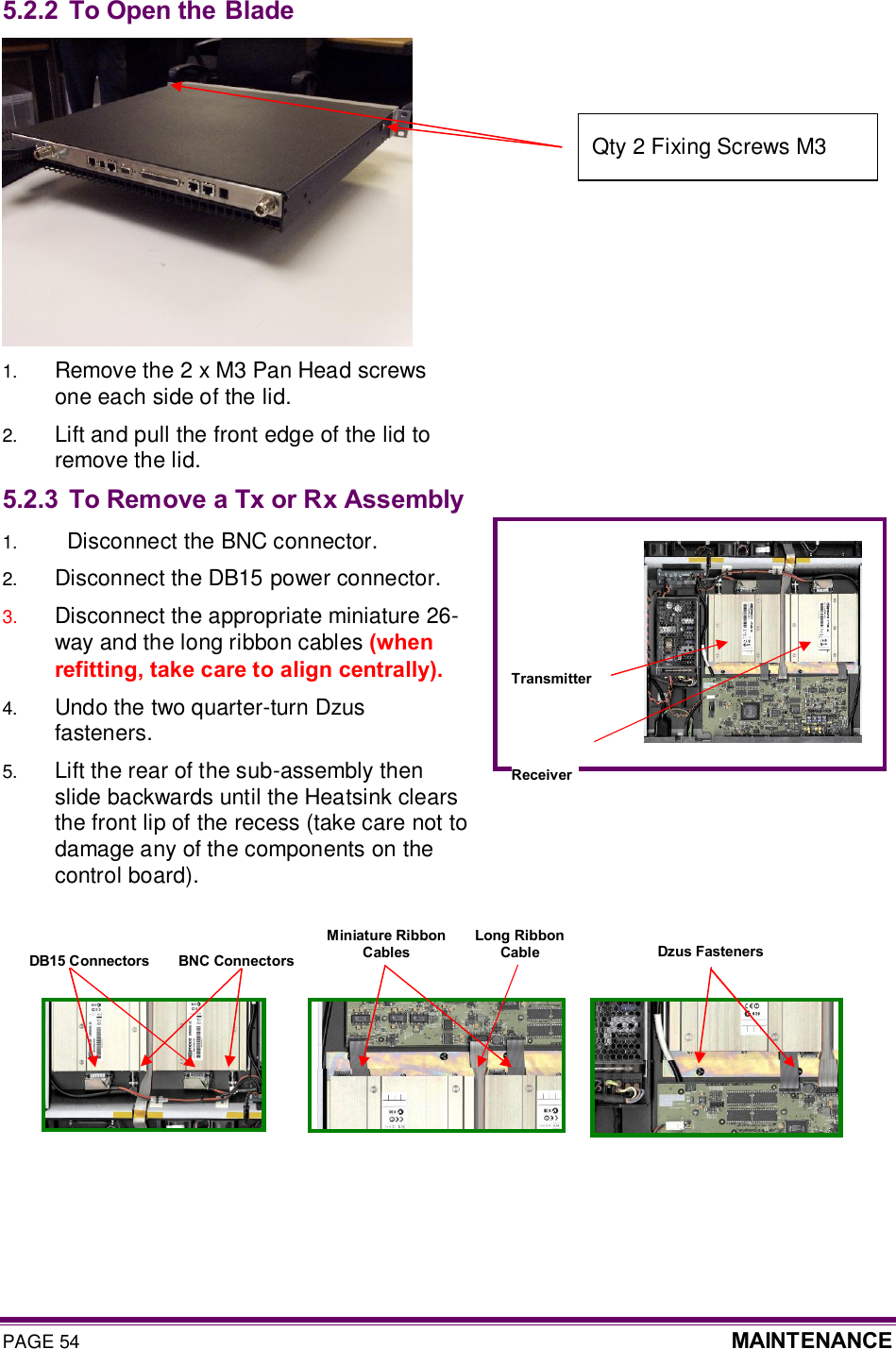
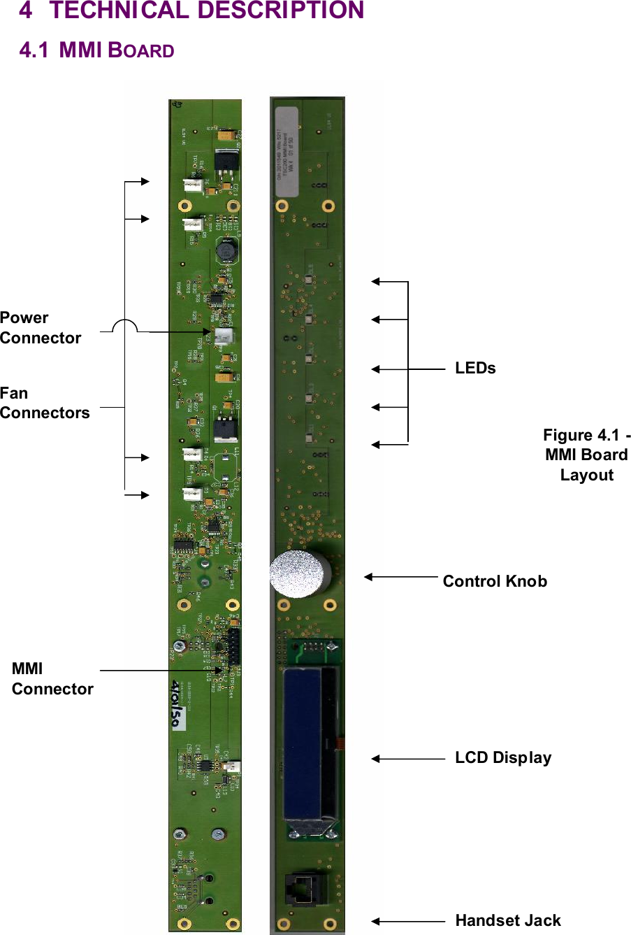
![PAGE 16 DESCRIPTION Tx Current Consumption Typical: 100W: 5.7A @13.6V + 6.0A @27.3V (20°C) Max: 100W: 8.85A @13.6V + 10.0A @27.3V (fans & audio on maximum) Duty Cycle 100% Audio Distortion <5% at 1kHz, 60% deviation Audio Frequency Response +1db to –3db of pre-emphasised 300 to 3000Hz on 25kHz channel, 300 to 2550Hz on 12.5kHz channel Hum and Noise >40db (12.5kHz), 45db (25kHz) Transmit Rise Time <25ms 3.3.3 Receiver Sensitivity Voice: ³12db SINAD for 0.3mVpd (typically >20db) for 25kHz channel. Data: typical FFSK performance for <10-2 BER (<20%MER): 0.3mVpd – 1200 baud in 12.5kHz & 1200/2400 baud in 25 kHz, 0.5mVpd – 2400 baud in 12.5kHz channel. [Ref: EN300-113-1:9.1] Rx Current Consumption Typical: 1.0A (20°C) Max: 1.55A (fans & audio on maximum) Selectivity >73db (25kHz), >63db (12.5kHz) Intermodulation >70db (ETSI method) Audio Response ±3dB of de-emphasised 300 to 3000Hz with CTCSS Audio Output 2Wrms internal monitor speaker Blocking >95dB at ±1Mhz Hum and Noise >40dB (12.5kHz) – CCITT weighted 3.4 FRONT PANEL CONTROLS 3.4.1 LED Indicators On the front of the Blade there are the following 5 LED indicators (from left to right): Legend Colour Description Power Green Indicates presence of 3.3V DC Tx Red Indicates unit is keyed up Rx Yellow Indicates RF signal received CC Orange Control Channel Activity Alm Red Alarm indicator – access LCD ‘alarms’ menu or connect PC to diagnose](https://usermanual.wiki/Simoco-EMEA/XFINBLATU.USERS-MANUAL/User-Guide-902013-Page-16.png)
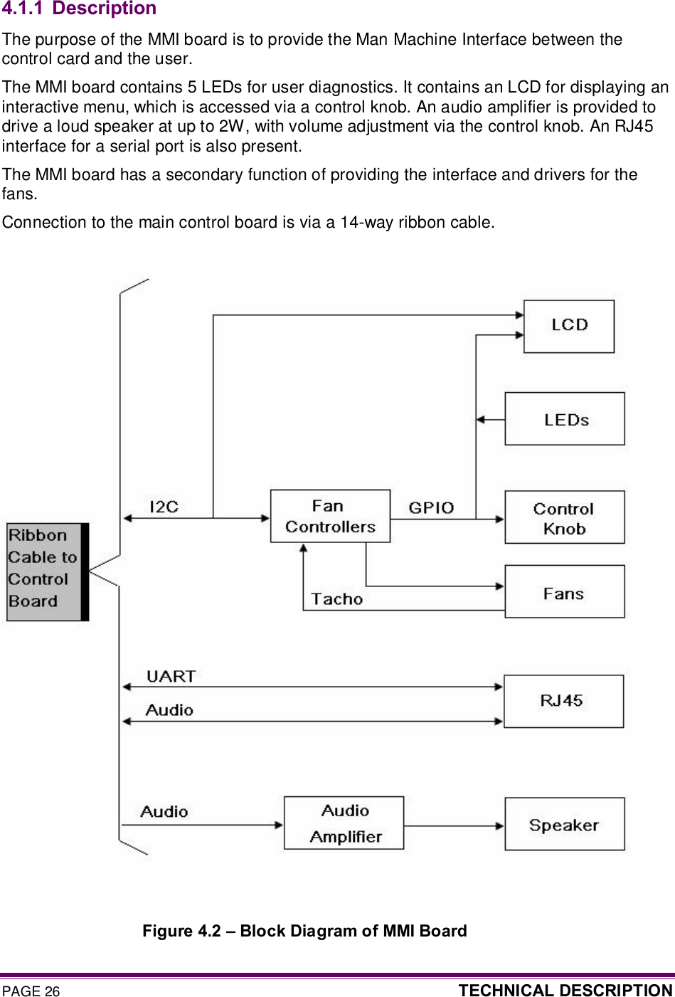
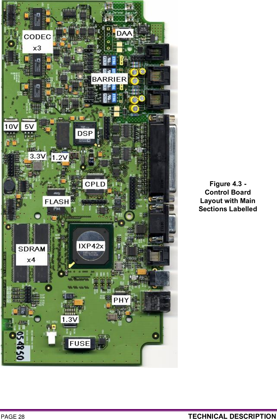
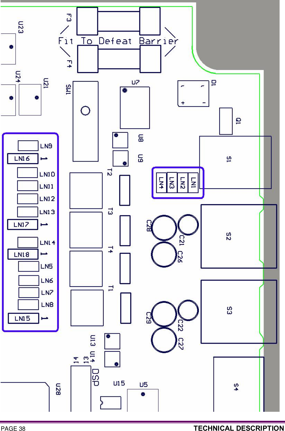
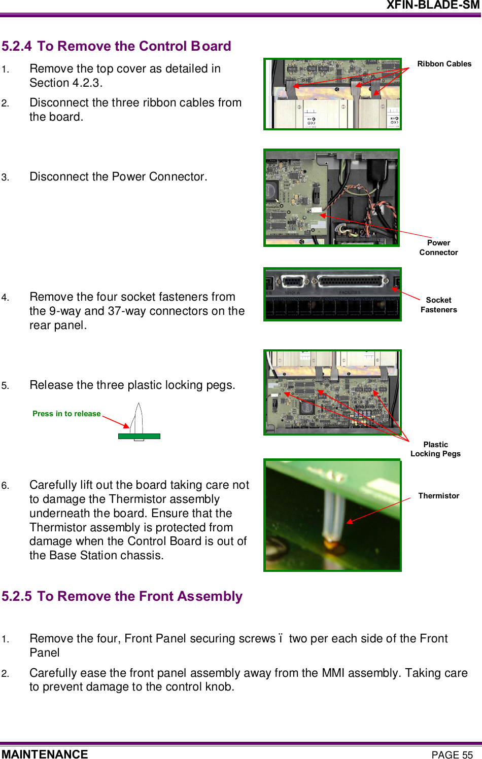
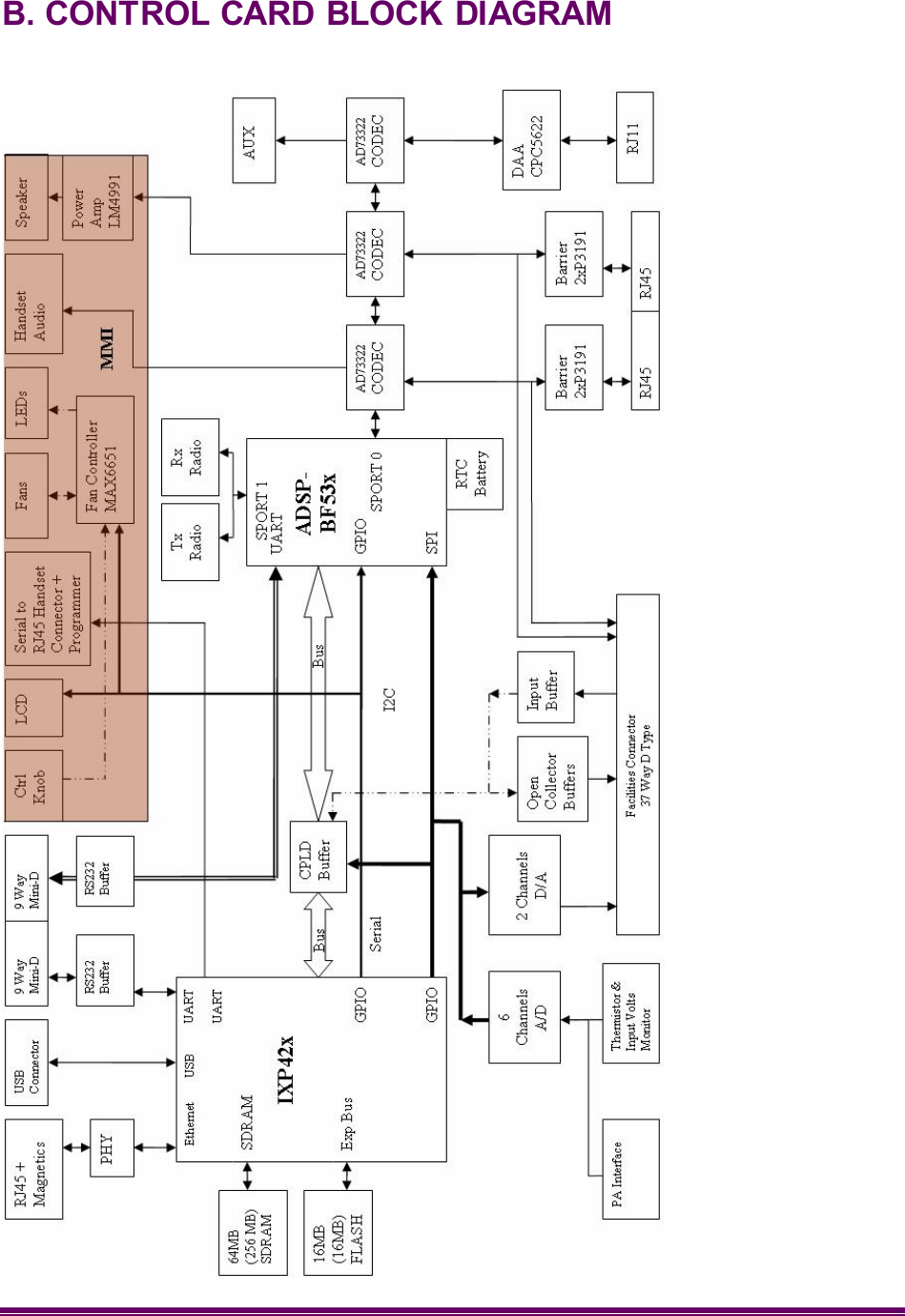
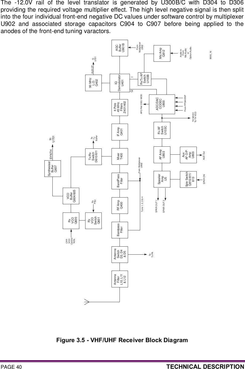
![XFIN-BLADE-SM TECHNICAL DESCRIPTION PAGE 39 4.3 RECEIVER AND TRANSMITTER MODULES 4.3.1 Frequency Bands The Blade is supplied with a matched pair of radio sub-assemblies fitted. The designated frequency bands are: 66 - 88 MHz E0 Band 335 - 375 MHz R1 Band 136 - 174 MHz AC Band 400 - 450 MHz TK Band 174 - 208 MHz K1 Band 400 - 480 MHz TU Band 208 - 245 MHz KM Band 440 - 500 MHz UW Band 310 - 350 MHz R0 Band 470 - 530 MHz WR Band The following text refers to the components and circuits within the RF sub-assemblies only. For additional information, refer to the SRM9000 Service Manual [1]. The Rx and Tx Modules are equivalent and interchangeable for a given power classification (25W or 100W). They are connected to the Control Board via a 26-way Ribbon Cable that carries analogue audio, digital audio and control signals. Power connections are made via a 15-way, D-type connector and RF connections are made via BNC sockets. RF connections are taken to the rear of the Blade via double-screened cables terminated with female N-types. 4.3.2 Receiver Refer to Figure 3.5. 4.3.2.1 Front-end Filters and Rx Front-end Amplifier The receiver input signal from the antenna passes through the antenna filter comprising L10, L11, L12 and associated tuning capacitors. With a transceiver module in receive mode, diodes D3, D4 and D5 in the antenna switch are reverse biased allowing the receiver input signal to be coupled through to the front-end with minimal loss. The overall insertion loss of the antenna filter and switch is approximately 0.8dB. Front-end selectivity is provided by varactor tuned bandpass filters at the input and output of the RF amplifier. Front-end tuning voltages are derived from the alignment data stored in the radio. The DSP processes this data to optimise front-end tuning relative to the programmed channel frequencies that may be changed at any time without re-aligning the radio. To achieve the required varactor tuning range an arrangement of positive and negative bias power supplies is used to provide a total bias across the varactors of up to 14.0VDC. A fixed 2.5V positive bias derived from the 5.0V supply and voltage divider R425/426 is applied to the cathodes of the varactor diodes. The negative bias supply originates at the DSP/FPGA as a composite digital tuning signal (FE TUNE) containing the data for the four front-end tuning values TUNE 1 to 4 for the particular channel frequency selected. The level is dependent on channel frequency and tuning and varies between +0.1 and +3.0V. This signal then passes through buffer U901A and level translator Q900 to Q903 where it is converted to a high level (-0.5 to -11.5V) negative equivalent of the original signal.](https://usermanual.wiki/Simoco-EMEA/XFINBLATU.USERS-MANUAL/User-Guide-902013-Page-39.png)
![PAGE 52 TECHNICAL DESCRIPTION 4.4 ANTENNA REQUIREMENTS The antenna connections on the Blade are provided with 50W female N-type sockets. These should be tested, by use of a suitable test set, e.g. Anritsu/Wiltron S331A, for good VSWR (1.5:1 or better) at the Tx and Rx frequencies prior to use. Mating connectors should be galvanically compatible with nickel outer and gold centre pin to minimise passive intermodulation. A minimum of 85dB transmit-receive isolation should be provided by the antenna system and associated filters. 4.5 POWER SUPPLIES For type approval reasons, this product should not be operated with un-approved supplies. The switch mode supplies used in the wall mount and rack mount ancillaries are able to accept main AC in the range of 100 to 240 V, 50 or 60Hz. The output from the switched mode power supply to the Blade is +13.6VDC. Pin 3 on the D-type Power Connector provides protective earthing on the equipment. This should be connected using heavy duty Green/Yellow earthing wire, capacity greater than mains feed to equipment, as few bends as possible and an appropriate eyelet tag. Mains protective Earth should be checked for low impedance (<0.3W). The equipment must be installed so that the IEC connector for the Wall or Rack Mount can be easily removed and/or the power socket should be readily accessible. All mains wiring must comply with local wiring regulations. 4.6 CONFIGURATION Configuration is provided via file download. This is performed via the XBMT Programmer using a PC connected to the Xfin Control card via its Ethernet port. Files are then stored in the product in non-volatile memory. Editing of parameters on a live base station is also possible with a connected PC. 4.7 ADJUSTMENT AND ALIGNMENT The two RF modules within this product are based upon the RF card of an SRM9000 mobile. The set up and alignment procedures for SRM9000 should be followed. In the event of a level-3 repair being required, refer to the SRM9000 Service Manual (TSD-SRM9000-SM) [1]. There are no user adjustments to be made in normal use.](https://usermanual.wiki/Simoco-EMEA/XFINBLATU.USERS-MANUAL/User-Guide-902013-Page-52.png)