Sony Ericsson Cdp Xe570 Users Manual
CDP-XE570 7bf601e9-b8df-4b3e-b2d4-63d89a13e339
CDP-XE570 to the manual 7bf601e9-b8df-4b3e-b2d4-63d89a13e339
2015-02-04
: Sony-Ericsson Sony-Ericsson-Cdp-Xe570-Users-Manual-388565 sony-ericsson-cdp-xe570-users-manual-388565 sony-ericsson pdf
Open the PDF directly: View PDF ![]() .
.
Page Count: 30
- Cover
- TABLE OF CONTENTS
- SERVICING NOTE
- GENERAL
- DISASSEMBLY
- TEST MODE
- ELECTRICAL BLOCK CHECKING
- DIAGRAMS
- CIRCUIT BOARDS LOCATION
- SCHEMATIC DIAGRAM LOADING MOTOR SECTION
- PRINTED WIRING BOARD LOADING MOTOR SECTION
- PRINTED WIRING BOARD BD SECTION
- SCHEMATIC DIAGRAM BD SECTION
- PRINTED WIRING BOARD MAIN SECTION
- SCHEMATIC DIAGRAM MAIN SECTION
- PRINTED WIRING BOARD DISPLAY SECTION
- SCHEMATIC DIAGRAM DISPLAY SECTION
- IC PINFUNCTIONS
- IC BLOCK DIAGRAMS
- EXPLODED VIEWS
- ELECTRICAL PARTS LIST
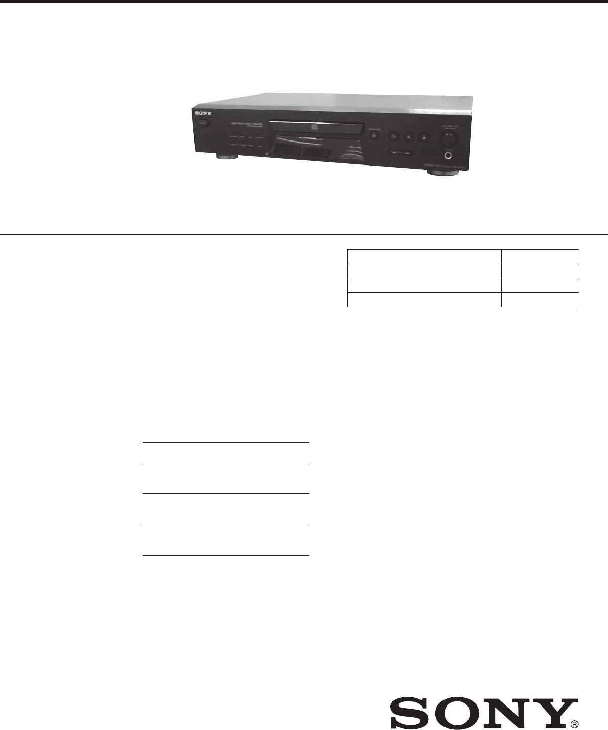
CDP-XE570
AEP Model
UK Model
SERVICE MANUAL
COMPACT DISC PLAYER
Sony Corporation
Audio Entertainment Group
General Engineering Dept.
9-873-878-11
2001C1600-1
© 2001.3
SPECIFICATIONS
Ver 1.0 2001. 03
Model Name Using Similar Mechanism NEW
CD Mechanism Type CDM66-5BD27
Base Unit Type BU-5BD27
Optical Pick-up Type PXR-104X
Compact disc player
Laser Semiconductor laser (λ =
780 nm)
Emission duration:
continuous
Frequency response 2 Hz to 20 kHz ± 0.5 dB
Dynamic range More than 93 dB
Harmonic distortion 0.0045%
Outputs
ANALOG
OUT
DIGITAL
OUT
(OPTICAL)
PHONES
General
Power requirements 230 V AC, 50/60 Hz
Power consumption 11 W
Dimensions (approx.) 430 x 95 x 290 mm
(w/h/d) incl. projecting parts
Mass (approx.) 3.3 kg
Supplied accessories
Audio cord (2 phono plugs – 2 phono plugs) (1)
Remote commander (remote) (1)
R6 (size AA) batteries (2)
Design and specifications are subject to change
without notice.
Load
impedance
Over 10
kilohms
Wave length:
660 nm
32 ohms
Jack
type
Phono
jacks
Optical
output
connector
Stereo
phone
jack
Maximum
output level
2 V
(at 50
kilohms)
–18 dBm
10 mW
Photo : BLACK
2
CDP-XE570
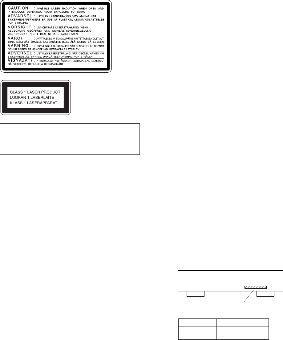
The following caution label is located inside of the unit.
This appliance is classified
as a CLASS 1 LASER
product.
The CLASS 1 LASER
PRODUCT MARKING is
located on the rear exterior.
CAUTION
Use of controls or adjustments or performance of procedures
other than those specified herein may result in hazardous
radiation exposure.
Notes on chip component replacement
• Never reuse a disconnected chip component.
• Notice that the minus side of a tantalum capacitor may be
damaged by heat.
Flexible Circuit Board Repairing
• Keep the temperature of soldering iron around 270˚C
during repairing.
• Do not touch the soldering iron on the same conductor of the
circuit board (within 3 times).
• Be careful not to apply force on the conductor when soldering
or unsoldering.
SAFETY-RELATED COMPONENT WARNING!!
COMPONENTS IDENTIFIED BY MARK 0 OR DOTTED LINE WITH
MARK 0 ON THE SCHEMATIC DIAGRAMS AND IN THE PARTS
LIST ARE CRITICAL TO SAFE OPERATION. REPLACE THESE
COMPONENTS WITH SONY PARTS WHOSE PART NUMBERS
APPEAR AS SHOWN IN THIS MANUAL OR IN SUPPLEMENTS
PUBLISHED BY SONY.
MODEL IDENTIFICATION
— BACK PANEL —
Parts No.
1. SERVICING NOTE ·························································· 3
2. GENERAL ·········································································· 6
3. DISASSEMBLY
3-1. Loading Panel ····································································· 7
3-2. Base Unit (BU-5BD27) ······················································ 7
4. TEST MODE
4-1. Check Mode ······································································· 8
4-2. AFADJ Mode ····································································· 8
4-3. ADJ Mode ·········································································· 9
5. ELECTRICAL BLOCK CHECKING························ 10
6. DIAGRAMS
6-1. Circuit Boards Location ··················································· 12
6-2. Schematic Diagram Loading Motor Section ·················· 13
6-3. Printed Wiring Board Loading Motor Section ················ 13
6-4. Printed Wiring Board BD Section ··································· 14
6-5. Schematic Diagram BD Section ······································ 15
6-6. Printed Wiring Board Main Section ································ 16
6-7. Schematic Diagram Main Section ··································· 17
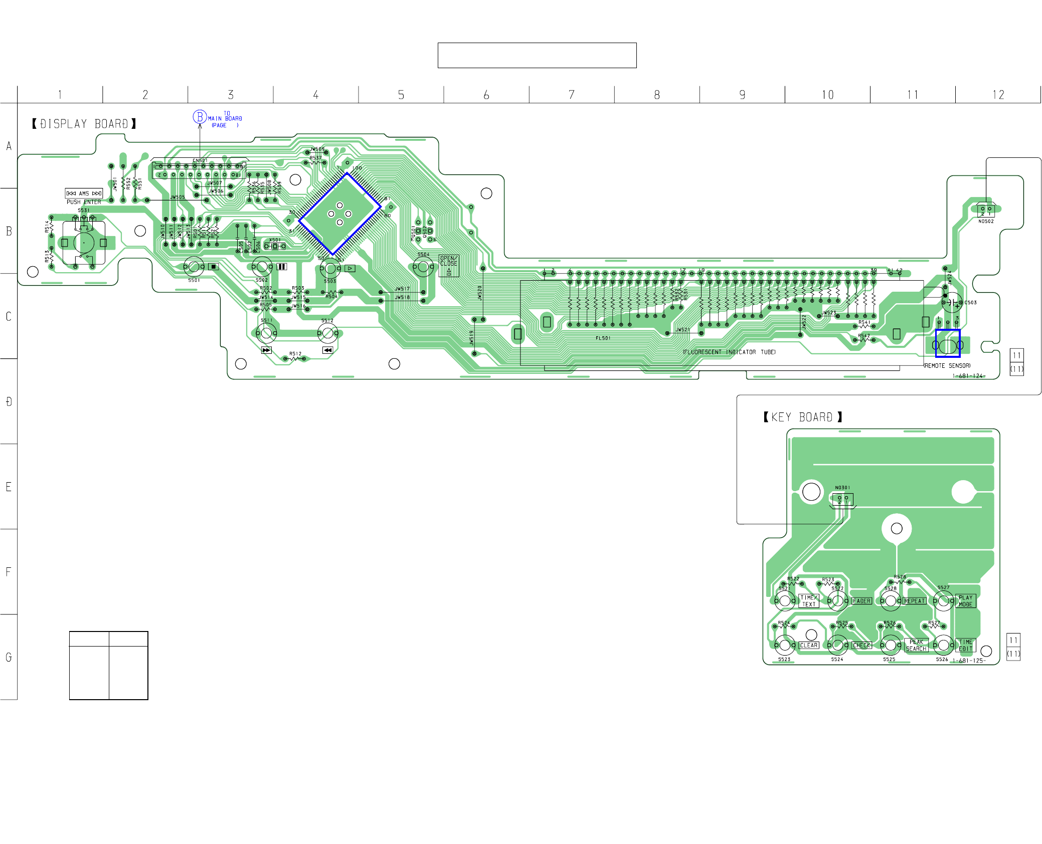
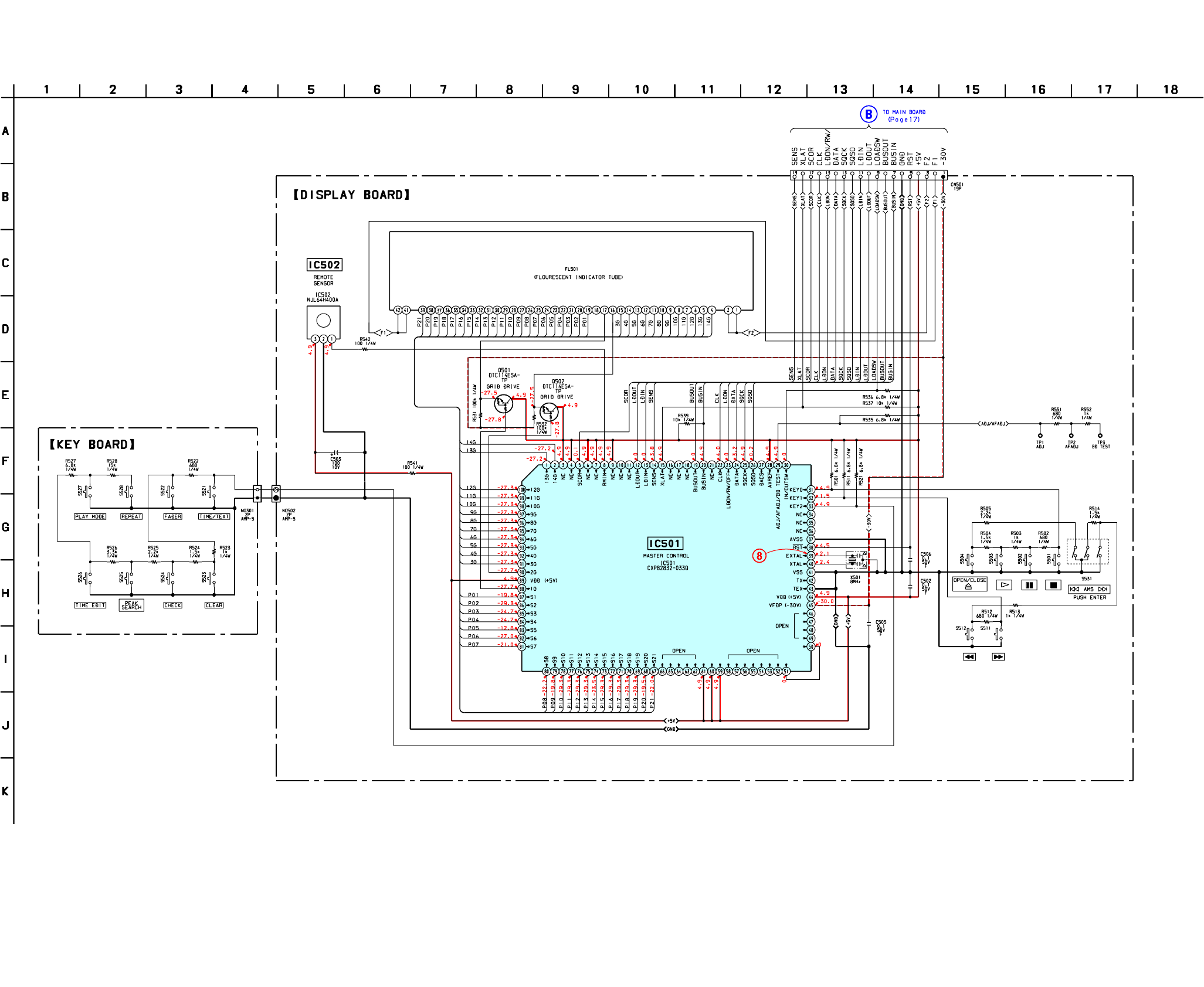
6-8. Printed Wiring Board Display Section ···························· 18
6-9. Schematic Diagram Display Section ······························· 19
6-10. IC Pinfunctions ································································· 20
6-11. IC Block Diagrams ··························································· 21
7. EXPLODED VIEWS
7-1. Front Panel and Case Section ··········································· 23
7-2. CD Mechanism Section (CDM66-5BD27) ······················ 24
7-3. Base Unit Section (BU-5BD27) ······································· 25
8. ELECTRICAL PARTS LIST ······································· 26
TABLE OF CONTENTS
PARTS No. MODEL
4-232-150-0s
4-232-150-1s
AEP
UK
3
CDP-XE570
SECTION 1
SERVICING NOTE
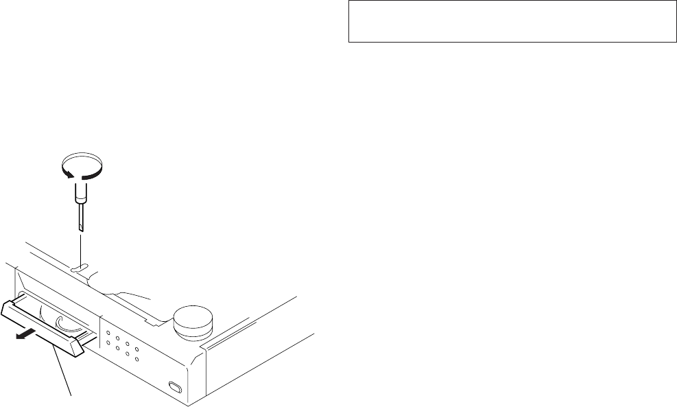
HOW TO OPEN THE DISC TRAY WHEN POWER SWITCH
TURNS OFF
Insert a tapering driver into the aperture of the unit bottom, and turn
in the direction of arrow.
Use a flat (–) head screwdriver to open the CD tray by manual opera-
tion. (Flat head screwdriver with nominal blade length of 3mm.)
*
To close the disc table, turn the driver in the reverse direction.
NOTES ON HANDLING THE OPTICAL PICK-UP BLOCK
OR BASE UNIT
The laser diode in the optical pick-up block may suffer
electrostatic breakdown because of the potential difference
generated by the charged electrostatic load, etc. on clothing and
the human body.
During repair, pay attention to electrostatic breakdown and also
use the procedure in the printed matter which is included in the
repair parts.
The flexible board is easily damaged and should be handled with
care.
NOTES ON LASER DIODE EMISSION CHECK
The laser beam on this model is concentrated so as to be focused
on the disc reflective surface by the objective lens in the optical
pick-up block. Therefore, when checking the laser diode emission,
observe from more than 30 cm away from the objective lens.
Pull out disc table.
4
CDP-XE570
Restrictions in CD-TEXT Display
In this unit, some special characters will not be displayed properly. These will be displayed as a space or a character resembling it. For details,
refer to “Table 2 : CD-TEXT DISC Recorded Contents and Display”.
Table 1 : CD-TEXT TEST DISC TEXT Data Contents (TRACKS No. 1 to 41:Normal Characters)
1
2
3
4
5
6
7
8
9
10
11
12
13
14
15
16
17
18
19
20
21
TRACK
No. Displayed Contents
22
23
24
25
26
27
28
29
30
31
32
33
34
35
36
37
38
39
40
41
TRACK
No. Displayed Contents
1kHz/0dB/L&R
20Hz/0dB/L&R
40Hz/0dB/L&R
100Hz/0dB/L&R
200Hz/0dB/L&R
500Hz/0dB/L&R
1kHz/0dB/L&R
5kHz/0dB/L&R
7kHz/0dB/L&R
10kHz/0dB/L&R
16kHz/0dB/L&R
18kHz/0dB/L&R
20kHz/0dB/L&R
1kHz/0dB/L&R
1kHz/-1dB/L&R
1kHz/-3dB/L&R
1kHz/-6dB/L&R
1kHz/-10dB/L&R
1kHz/-20dB/L&R
1kHz/-60dB/L&R
1kHz/-80dB/L&R
1kHz/-90dB/L&R
Infinity Zero w/o emphasis//L&R
Infinity Zero with emphasis//L&R
400Hz+7kHz(4:1)/0dB/L&R
400Hz+7kHz(4:1)/-10dB/L&R
19kHz+20kHz(1:1)/0dB/L&R
19kHz+20kHz(1:1)/-10dB/L&R
100Hz/0dB/L*
1kHz/0dB/L*
10kHz/0dB/L*
20kHz/0dB/L*
100Hz/0dB/R*
1kHz/0dB/R*
10kHz/0dB/R*
20kHz/0dB/R*
100Hz Squer Wave//L&R
1kHz Squer Wave//L&R
1kHz w/emphasis/-0.37dB/L&R
5kHz w/emphasis/-4.53dB/L&R
16kHz w/emphasis/-9.04dB/L&R
NOTE : The contents of Track No. 1 to 41 are the same as those of the current TEST DISC-their titles are displayed.
However, only 8 digits are displayed, and the 9th digit onwards are displayed as “– – – – –”.
CD-TEXT TEST DISC
This unit is able to display the TEXT data (character information)
written in the CD on its fluorescent indicator tube.
The CD-TEXT TEST DISC (TGCS-313: J-2501-126-A) is used
for checking the display.
To check, perform the following procedure.
Procedure:
1. Turn ON the power and set the test disc.
2. Press the H button and play back the disc.
3. The following will be displayed on the fluorescent indicator
tube.Display : 1kHz/0 dB/– – – –
4. Rotate the l AMS L knob to switch the track. The
text data of each track will be displayed.
5
CDP-XE570
!”#$%&´(21h to 27h)1kHz 0dB L&R
( ) +,–. / (28h to 2Fh)
01234567 (30h to 37h)
8 9 : ; < = > ? (38h to 3Fh)
@A B C D E F G (40h to 47h)
H I J K L M N O (48h to 4Fh)
P Q R S T U VW (50h to 57h)
XYZ [ ¥] ^ _ (58h to 5Fh)
a b c d e f g (60h to 57h)
h i j k l m n o (68h to 6Fh)
p q r s t u v w (70h to 77h)
xyz{ I } (78h to 7Fh)
i¢£¤¥ § (A0h to A7h) 8859-1
9Cª¬PR–(A8h to AFh)
•±23 µ¶• (B0h to B7h)
†1º ¿ (B8h to BFh)
ÀÁÂÃÄÅÆÇ (C0h to C7h)
ÈÉÊËÌÍÎÏ (C8h to CFh)
DÑÒÓÔÕÖ (D0h to C7h)
ØÙÚÛÜYß(D8h to DFh)
àáâãäåæç (E0h to E7h)
èéêëìíîï (E8h to FFh)
∂ñòóôõö÷(F0h to F7h)
øùúûüyÿ(F8h to FFh)
No.66
No.67
to
No.99
TRACK
No. Recorded contents Display
···· ! ” # $ % & are not displayed
() + –/···· , . are not displayed
01234567····
89 = ?···· : ; < > are not displayed
ABCDEFG···· @ is not displayed
HIJKLMNO····
PQRSTUVW····
XYZ[/]^_····
ABCDEFG····
HIJKLMNO····
PQRSTUVW····
XYZ ···· { I } are not displayed
···· i ¢ £ ¤ ¥ § are not displayed
¬–
···· 9 C ª P R are not displayed
±···· 2 3 µ ¶ • are not displayed
¿ ···· † 1 º are not displayed
ÀÁÂÃÄÅ ···· Æ Ç are not displayed
ÈÉÊËÌÍÎÏ····
ÑÒÓÔÕÖ ····D are not displayed
ÙÚÛÜY····Ø ß are not displayed
ÀÁÂÃÄÅ ····æ ç are not displayed
ÈÉÊËÌÍÎÏ····
ÑÒÓÔÕÖ ····∂ ÷ are not displayed
ÙÚÛÜY···ø ÿ are not displayed
T All the same
T All the same
to
T All the same
′
*
42
43
44
45
46
47
48
49
50
51
52
53
54
55
56
57
58
59
60
61
62
63
64
65
66
67
to
99
~
1
41
23
4
′
˙
1
41
23
4
Table 2: CD-TEXT TEST DISC Recorded Contents and Display
(In this unit, some special characters cannot be displayed. This is not a fault.)
´
*
′
~
´
´
.
...
′
6
CDP-XE570 SECTION 2
GENERAL
FRONT PANEL
CHECK qf (12)
CLEAR qg (12)
Disc compartment 6 (8)
Display qj (10)
FADER 4 (13)
PEAK SEARCH qd (14)
PHONES jack ql (9)
PLAY MODE 2 (9, 12, 14)
POWER 1 (8)
Remote sensor qh (7)
REPEAT 3 (9, 11)
TIME EDIT qs (13, 14)
TIME/TEXT 5 (10)
BUTTON DESCRIPTIONS
A OPEN/CLOSE 7 (8, 10, 12)
H 8 (9, 11, 12, 14)
X 9 (9, 14)
x 0 (9, 14)
lAMSL dial qa (9, 12, 14)
m/M qk (9, 13)
ANALOG OUT L/R jacks 2 (7)
CONTROL A1II jacks 3 (8, 15)
DIGITAL OUT OPTICAL jack 1 (8)
Mains lead 4 (7)
BACK PANEL
This section is extracted
from instruction manual.
7
CDP-XE570
SECTION 3
DISASSEMBLY
Note : Follow the disassembly procedure in the numerical order given.
3-1. LOADING PANEL
•In order to remove the front panel block when the power supply
does not turn on, rotate the cam with tapering driver as the figure
shows, and the loading part will be moved.
Then pull out the loading part by your hand to remove the loading
panel as the figure shows. After that take out the front panel block.
3-2. BASE UNIT (BU-5BD27)
Tapering driver
Loading part
Loading panel
4 Remove the Base unit
(BU-5BD27) to the direction
of arrow.
1 Turn the cam to the direction of
arrow (counter clock wise) by
tapering driver.
2 Take off the tray.
3 Screw (DIA. 12), floating
BU-5BD27
8
CDP-XE570 SECTION 4
TEST MODE
4-1. CHECK MODE
The following checks can be performed in the CHECK Mode.
• Offset value display
1. Turn on the set.
2. Put disc in the set.
3. Press the [PLAY MODE] , H and M buttons simultaneously.
4. The Offset measured values will be displayed as “AB 02 FE”
(typical values).
• RFDC value display
1. Turn on the set.
2. Put disc in the set.
3. Press the [PLAY MODE], H and m buttons simultaneously.
4. The RFDC measured value will be displayed as “RFDC 65”
(typical value). If there is no disc in the set, “RFDC NO” will
be displayed.
4-2. AFADJ MODE
The following checks can be performed in the AFADJ mode, which
is set by connecting the TP2 (AFADJ) terminal on DISPLAY
BOARD to the Ground and turning on the power.
• FL tube check
After all segments light up, when the H button is pressed, the
following will be displayed.
When the x button is pressed, the following will be displayed.
A B C D E F
42
1412
6810
16 18 20
The display will light up as follows when the l AMS L
knob is rotated to the right, and as follows when rotated to the
left.
When the OPEN/CLOSE A button is pressed, all will light up
again.
• Key check
All buttons have corresponding button numbers. When a button
is pressed, the counter will count up and display the button’s num-
ber. However, the counter will only count to “15”. It will not count
for buttons already pressed once, but will display the button’s
number.
88 TOTAL= 88
XX
Display of button number Display of counting
JOG RIGHT
JOG LEFT
Button
X
M
m
ENTER(AMS)
TIME/TEXT
FADER
CLEAR
CHECK
Buttton No.
Displayed
1
8
9
10
16
17
18
19
Button
PEAK SEARCH
TIME EDIT
PLAY MODE
REPEAT
OPEN/CLOSE
A
PLAY H
STOP x
Button No.
Displayed
20
21
22
23
All lit
(ABCDEF)
(Music Calendar)
• Remote commander check
When the “ H ” button is pressed, the display will light up
as follows.
REMOCON PLAY
9
CDP-XE570
4-3. ADJ MODE
The following operations are performed in the ADJ mode, which is
set by connecting the TP1 (ADJ) terminal to the Ground and turning
on the power.
Table of Button Operations in ADJ Mode
The functions of the buttons are shown in the following table.
Function of Buttons
* NOTE : Other buttons are not used for servicing and should not
be pressed without a reason.
Button
TIME/TEXT
M
m
CLEAR
Function
Tracking servo ON/OFF
OFFSET(VC)/EF.BIAS display
OFFSET(RF,FE,TRK) display
RFCK/GFS/ERROR RATE check mode
TP2
AFADJ
TP1
ADJ
GND
S531
l AMS L
[ DISPLAY BOARD ] – Conductor side –
10
CDP-XE570
Procedure :
1. Connect oscilloscpe to test point TP (TE1) and TP (VC) on
BD BOARD.
2. Turn Power switch on.
3. Put disc (PATD-012) in to play the number five track.
4. Press the X (Pause) button. (Becomes the 1 track jump mode)
5. Check the level B of the oscilliscope's waveform and the A
(DC voltage) of the center of the Traverse waveform.
Confirm the following :
A/B x 100 = less than ± 22%
E-F Balance Check
Procedure :
1. Connect the test point TP1 (ADJ) on DISPLAY BOARD to
the ground with a lead wire on main board.
2. Connect oscilloscpe to test point TP (TE1) and TP (VC) on
BD BOARD.
3. Turn the Power switch on to set the ADJ mode.
4. Put disc (PATD-012) in to play the number five track.
5. Press the [TIME/TEXT] button. (The tracking servo are turned
OFF.)
6. Check the level B of the oscilliscope's waveform and the A
(DC voltage) of the center of the Traverse waveform.
Confirm the following :
A/B x 100 = less than ± 22%
Traverse waveform
oscilloscope
BD board
TP (TE1)
TP (VC)
0V
level : 1.15 ± 0.5 Vp-p
A (DC voltage)
Center of the waveform
B
0V
C (DC
voltage
)
Tracking servo
OFF
Tracking servo
ON
SECTION 5
ELECTRICAL BLOCK CHECKING
Note:
1. CD Block is basically designed to operate without adjustment.
Therefore, check each item in order given.
2. Use PATD-012 disc (3-702-101-01) unless otherwise indicated.
3. Use an oscilloscope with more than 10MΩ impedance.
4. Clean the object lens by an applicator with neutral detergent
when the signal level is low than specified value with the
following checks.
VOLT/DIV : 200mV
TIME/DIV : 500ns
level : 1.35 ± 0.4 Vp-p
oscilloscope
BD board
TP (TE1)
TP (VC)
0V
level : 1.15 ± 0.5Vp-p
A (DC voltage)
Center of the waveform
B
symmetry
RF Level Check
oscilloscope
BD board
TP (RF AC)
TP (VC)
Procedure :
1. Connect oscilloscope to test point TP (RF AC) and TP (VC) on
BD BOARD.
2. Connect the test point TP1 (ADJ) on DISPLAY BOARD to the
ground with a lead wire.
3. Turn Power switch on.
4. Put disc (PATD-012) in to play the number five track.
5. Press the [CLEAR] buton and select the RFCK function.
6. Confirm that oscilloscope waveform is clear and check RF
signal level is correct or not.
Note:
A clear RF signal waveform means that the shape “◊” can be clearly
distinguished at the center of the waveform.
RF signal waveform
E-F Balance (1 Track Jump) Check
1 track jump waveform
7. Press the [TIME/TEXT] button. (The tracking servo are turned
ON.) Confirm the C (DC voltage) is almost equal to the A (DC
voltage) is step 6.
Traverse waveform
8. Disconnect the lead wire of TP1 (ADJ) connected in step 1.
11
CDP-XE570
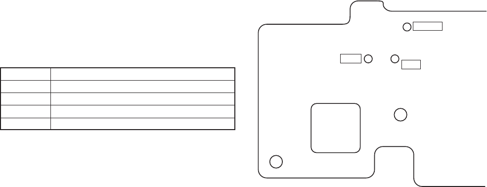
[ BD BOARD ] – Side B –
Adjustment Location :
[ DISPLAY BOARD ] – Conductor side –
CN102
IC101
TP(FE1)
TP(TE1)
TP(VC)
TP(RF AC)
TP2
AFADJ
TP1
ADJ
GND
S531
l AMS L
12
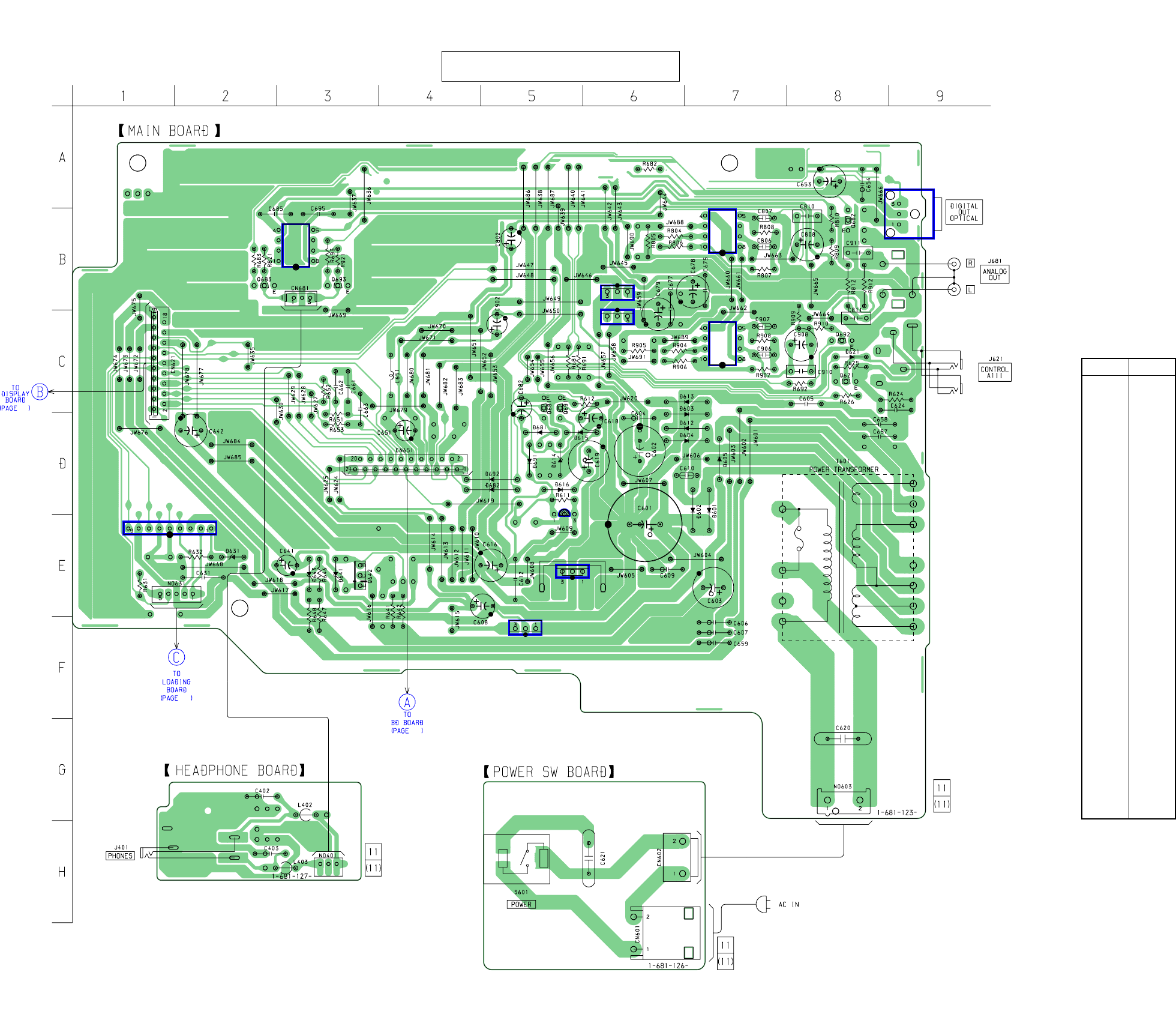
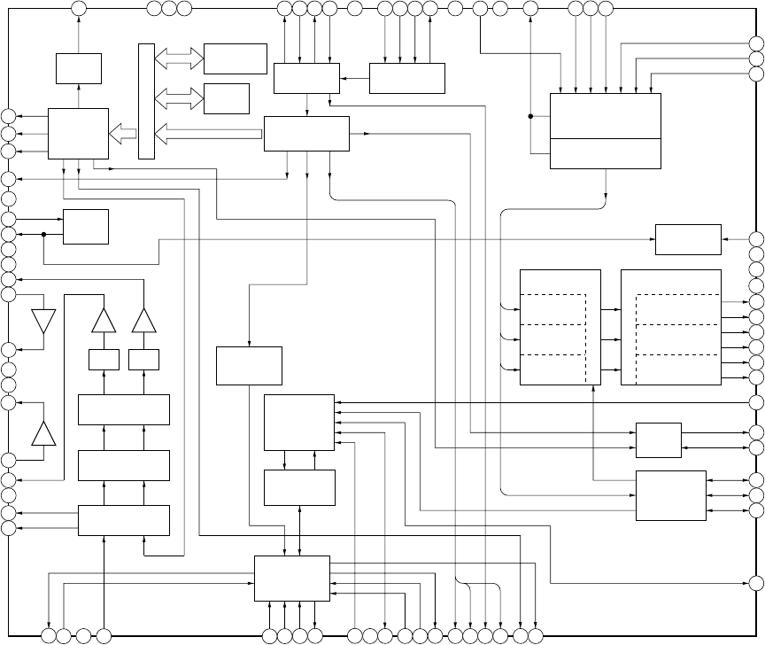
CDP-XE570 SECTION 6
DIAGRAMS
6-1. CIRCUIT BOARDS LOCATION
KEY board
DISPLAY board
HEADPHONE board
MAIN board
BD board
LOADING board
POWER SW board
1313
CDP-XE570
THIS NOTE IS COMMON FOR PRINTED WIRING
BOARDS AND SCHEMATIC DIAGRAMS.
(In addition to this, the necessary note is printed
in each block.)
For schematic diagrams.
Note:
• All capacitors are in µF unless otherwise noted. pF: µµF
50 WV or less are not indicated except for electrolytics
and tantalums.
• All resistors are in Ω and 1/4 W or less unless otherwise
specified.
•f: internal component.
•C: panel designation.
•A: B+ Line.
•B: B– Line.
• Voltages and waveforms are dc with respect to ground
under no-signal (detuned) conditions.
no mark : STOP
( ) : PLAY
• Voltages are taken with a VOM (Input impedance 10 MΩ).
Voltage variations may be noted due to normal produc-
tion tolerances.
• Waveforms are taken with a oscilloscope.
Voltage variations may be noted due to normal produc-
tion tolerances.
• Circled numbers refer to waveforms.
• Signal path.
J: CD
c: digital out
For printed wiring boards.
Note:
•X: parts extracted from the component side.
•Y: parts extracted from the conductor side.
•x: parts mounted on the conductor side.
•a: Through hole.
•b: Pattern from the side which enables seeing.
(The other layers' patterns are not indicated.)
Caution:
Pattern face side: Parts on the pattern face side seen from the
(Side B) pattern face are indicated.
Parts face side: Parts on the parts face side seen from the
(Side A) parts face are indicated.
• Indication of transistor
C
These are omitte
d
EB
Q
C
These are omitte
d
EB
Note: The components identified by mark 0 or dotted line
with mark 0 are critical for safety.
Replace only with part number specified.
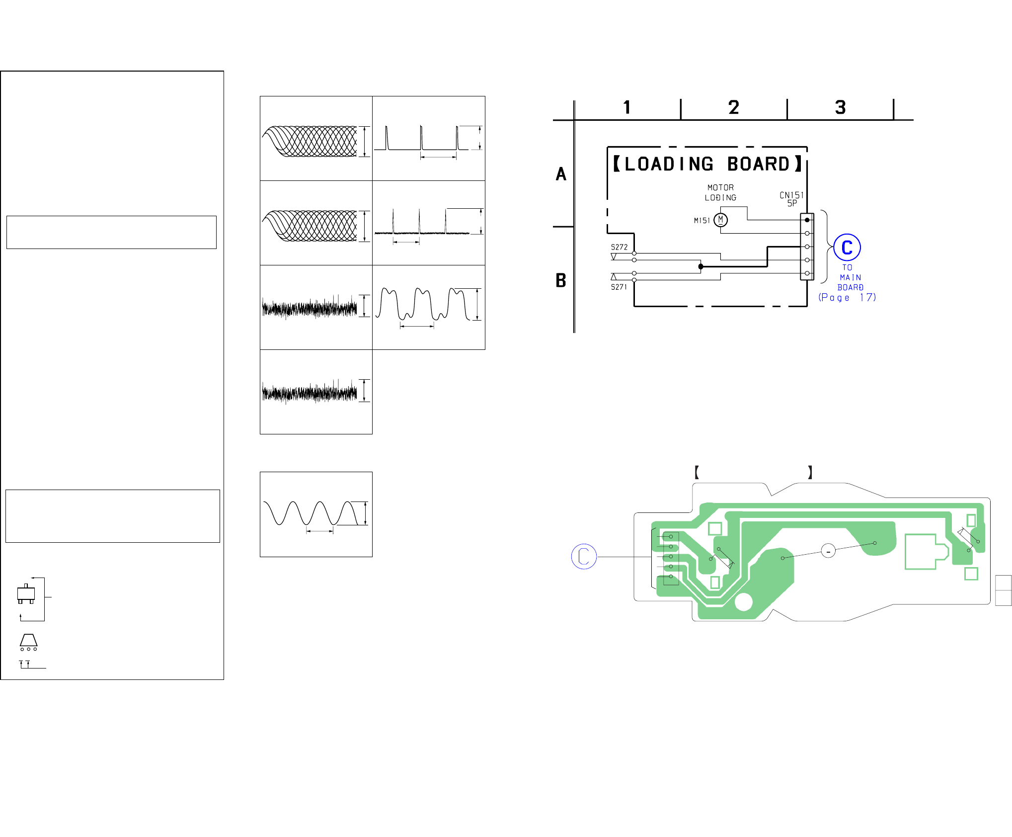
6-2. SCHEMATIC DIAGRAM LOADING MOTOR SECTION
11
(21)
S272
LOAD
IN
S271
LOAD
OUT
CN151
1
5
M151
LOADING
MOTOR
M
LOADING BOARD
1-645-721-
TO MAIN BOARD
(Page 16)
6-3. PRINTED WIRING BOARD LOADING MOTOR SECTION • See page 12 for Circuit Board Location.
1.3 Vp-p
5.2 Vp-p
13.4 ms
4.5 Vp-p
40 ns
5.9 Vp-p
59 ns
approx.
200 mVp-p
2.7 V
7.5
µ
s
1 IC101 ta (RFAC)
(CD Play Mode)
3 IC101 el (FE)
(CD Play Mode)
1.4 Vp-p
approx.
400 mVp-p
4 IC101 ra (TE)
(CD Play Mode)
8 IC501 el (EXTAL)
5 IC101 wh (MDP)
(CD Play Mode)
6 IC101 w; (SCOR)
(CD Play Mode)
7 IC101 yj (XTAO)
(CD Play Mode)
2 IC101 rd (RFD)
(CD Play Mode)
• WAVEFORMS
– BD Board –
– DISPLAY Board –
1616
CDP-XE570
6-6. PRINTED WIRING BOARD MAIN SECTION • See page 12 for Circuit Board Location. There are a few cases that the part printed on
this diagram isn’t mounted in this model.
IC681
IC631
IC801
IC651
IC901
IC601
IC602
IC603
IC671
IC672
18
13
14
Ref. No. Location
D601 D-7
D602 D-7
D603 C-7
D604 D-7
D605 D-7
D612 D-7
D613 C-7
D614 D-5
D615 D-5
D616 D-5
D621 C-8
D631 E-2
D641 E-3
D643 E-3
D681 D-5
D682 D-5
D691 D-5
D692 D-5
IC601 E-5
IC602 F-5
IC603 D-5
IC631 E-1
IC651 A-9
IC671 B-6
IC672 C-6
IC681 B-3
IC801 B-7
IC901 C-7
Q621 C-8
Q642 E-3
Q681 C-5
Q682 B-8
Q683 B-2
Q691 C-5
Q692 C-8
Q693 B-3
•Semiconductor
Location
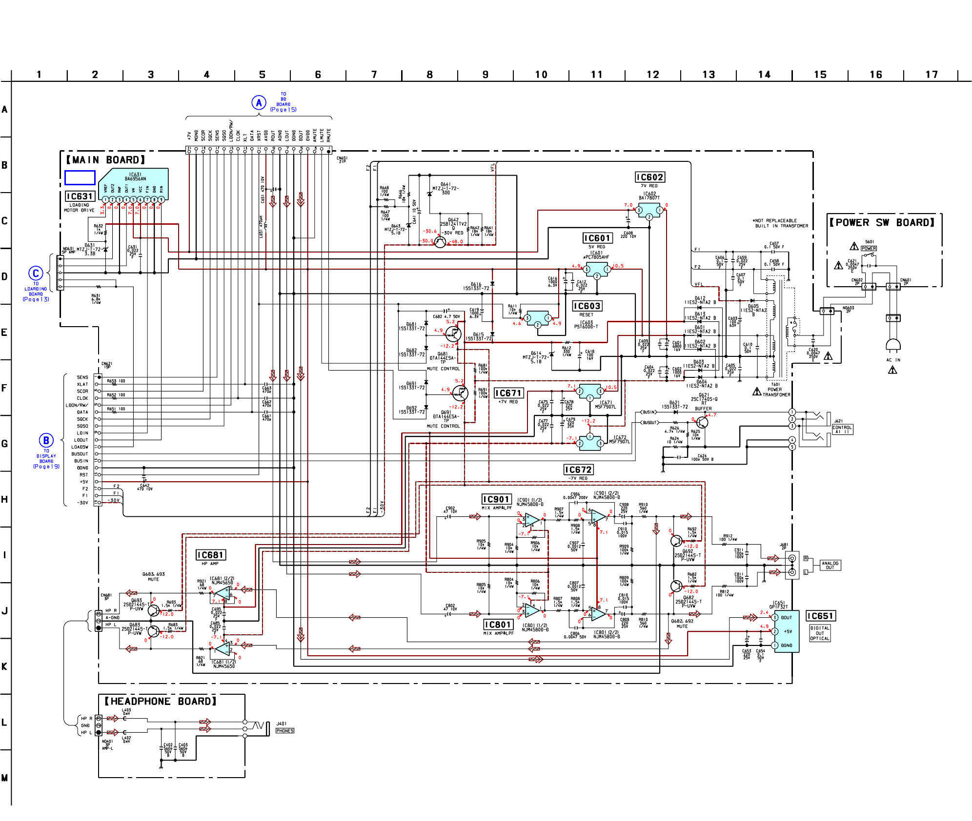
2020
CDP-XE570
6-10. IC PINFUNCTIONS
•Abbreviation
FL : Fluorescent indicator tube
Pin No. Pin Name I/O Function
41 VSS –Ground
42 TX –Not used
43 TEX –Connected to ground
44 VDD (+5V) –Power supply (+5V)
45 VFDP (–30V) –Pull down voltage (–30V)
46 XSEL O Not used
47 —–Not used
48 to 58 OPEN –Not used
59 to 61 VDD (+5V) –Power supply (+5V)
62 to 66 OPEN –Not used
67 to 87 S21 to S1 O FL segment signal output
88 1G O FL grid signal output
89 VDD (+5V) –Power supply (+5V)
90 to 100 2G to 12G O FL grid signal output
• IC501 MASTER CONTROL (CXP82832-033Q)(DISPLAY BOARD)
Pin No. Pin Name I/O Function
1 13G O FL grid signal output
2 14G O FL grid signal output
3NC–Connected to VDD
4NC–Connected to VDD
5 SCOR I Sub code sync input
6, 7 NC I Connected to VDD
8 RMIN I Remote control signal input
9NC–Connected to VDD
10, 11 NC –Not used (Open)
12 LD OUT O Loading motor control
13 LD IN I Loading motor control
14 SENS I Sense signal input
15 XLT O Serial latch output
16 NC O Not used (Open)
17 NC O Not used (Open)
18 NC –Not used (Open)
19 BUSOUT O CONTROL-A1 transmission output
20 BUSIN I CONTROL-A1 receive input
21 NC –Not used (Open)
22 CLK O Serial clock output
23 LDON/RW/OFF O Optical pick-up laser diode control output
24 DATA O Serial data output
25 SQCK O Subcode Q data readout clock output
26 SQSO I Subcode Q data input
27 DACS O Not used (Open)
28 AVREF I Analog reference voltage input
29 ADJ/AFADJ/BD TEST I Test mode terminal
30 IN/OUT SW I IN SW/OUT SW
31 KEY 0 I Key input
32 KEY 1 I Key input
33 KEY 2 I Key input
34 NC O Not used (Open)
35 NC O Not used (Open)
36 NC O Not used (Open)
37 AVSS –Analog ground
38 RST I Reset signal input
39 EXTAL I 8 MHz clock input
40 XTAL O 8 MHz clock output
•Abbreviation
FL : Fluorescent indicator tube
21
CDP-XE570
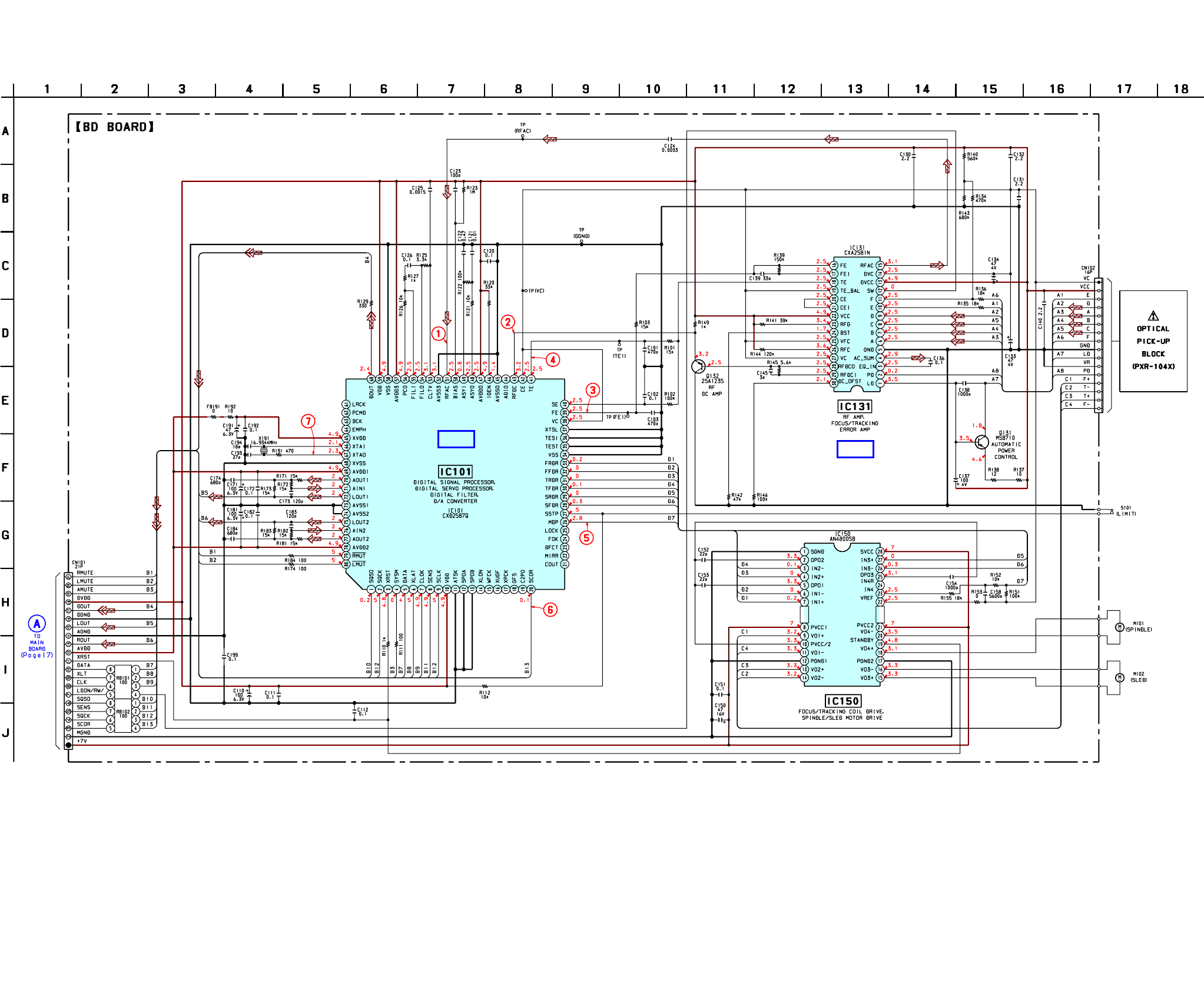
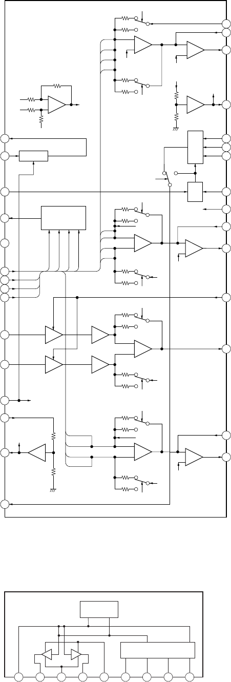
IC101 CXD2587Q (BD BOARD)
6-11. IC BLOCK DIAGRAMS
TE
RFDC
CE
IGEN
AVSS0
ADIO
AVDD0
CLTV
FILO
AVSS3
VSS
AVDD3
DOUT
VDD
PCO
FILI
ASYO
ASYI
RFAC
BIAS
SSTP
DFCT
MIRR
MDP
LOCK
FOK
SFDR
VSS
TEST
FRDR
FE
VC
COUT
SE
XTSL
TES1
SRDR
TFDR
FFDR
TRDR
2
1
70
71
68
69
66
67
64
65
62
61
63
73
74
72
75
76
77
78
79
80
4
XRST
3
SQCK
SQSO
59
8
7
6
56
60 53
54
55
59 57
58 51
52 48
49
50 47 44
45
46 43 41
42
XLAT
CLOK
SENS
SYSM
DATA
XUGF
XPCK
GFS
C2PO
WFCK
10 11 12 13 14 15 16 17 18 19 20
21
22
23
24
25
26
32
33
30
31
36
37
34
35
39
40
38
28
27
29
SPOA
ATSK
SCLK
VDD
SCOR
SPOB
XLON
XTAI
XVDD
EMPH
AVDD1
AOUT1
AIN1
XTAO
XVSS
AIN2
AOUT2
AVDD2
RMUT
LOUT2
LOUT1
BCK
LRCK
PCMD
LMUT
AVSS1
AVSS2
CPU
INTERFACE
SERVO AUTO
SEQUENCER
SERIAL IN
INTERFACE
OVER SAMPLING
DIGITAL FILTER
3rd ORDER
NOISE SHAPER
PWM PWM
EFM
DEMODULATOR
TIMING
LOGIC
DIGITAL
OUT
D/A
INTERFACE
DIGITAL
PLL
ASYMMETRY
CORRECTION
CLOCK
GENERATOR
MIRR, DFCT,
FOK
DETECTOR
DIGITAL
CLV
SUBCODE
PROCESSOR
SERVO
INTERFACE
SERVO DSP
FOCUS
SERVO
TRACKING
SERVO
SLED
SERVO
PWM GENERATOR
FOCUS PWM
GENERATOR
TRACKING
PWM GENERATOR
SLED PWM
GENERATOR
16K
RAM
ERROR
CORRECTOR
INTERNAL BUS
A/D
CONVERTER
OPERATIONAL
AMPLIFIER
ANALOG SWITCH
22
CDP-XE570
IC131 CXA2518N-T4 (BD BOARD)
IC631 BA6956AN (MAIN BOARD)
123456789
CONTROL LOGIC
TSD
VREF
OUT2
OUT1
RNF
VM
VCC
FIN
GND
RIN
RW/ROM
RW/ROM
EQ ON/OFF
VOFST
VOFST
DVC
VC
VC
VC
RW/ROM
VC
DVC
30
29
28
+
–
+
–
DVC
VCC
DVC
27
26
25
24
RW/ROM
EQ
23
22
21
20
19
RFAC
VCA
VCC
+
–
DVC
+
–
+
–
RW/ROM
VC
RW/ROM
DVC
+
–
3
A
B
C
D
B
C
A
A
A
B
C
D
BCD D
+
–
1
2APC AMP
5
6
7
8
9
4
RFAC
SUMMING
AMP
RW/ROM
APC-OFF
(Hi-Z)
RW/ROM
(H/L)
VOFST
VC
RW/ROM
+
–
10
11
GM
GM
18
17
16
B
D
A
C
13
14
15
12
EQ IN
LD
PD
GND
A
B
C
D
AC SUM
E
F
DVCC
DVC
RFAC
SW
DC OFST
RFDCI
RFDCO
VC
RFC
VFC
BST
RFG
VCC
CEI
CE
TE BAL
TE
FEI
FE
SECTION 7
EXPLODED VIEWS
NOTE:
• -XX, -X mean standardized parts, so they may
have some differences from the original one.
• Items marked “*” are not stocked since they
are seldom required for routine service. Some
delay should be anticipated when ordering these
items.
• The mechanical parts with no reference number
in the exploded views are not supplied.
• Hardware (# mark) list and accessories and
packing materials are given in the last of this
parts list. The components identified by mark 0 or
dotted line with mark 0 are critical for safety.
Replace only with part number specified.
23
CDP-XE570
• Color Indication of Appearance Parts Example:
KNOB, BALANCE (WHITE) . . . (RED)
↑ ↑
Parts of Color Cabinet’s Color
Ref. No. Part No. Description Remarks Ref. No. Part No. Description Remarks
7-1. FRONT PANEL AND CASE SECTION
27
12
23
22
27
27
18
19
20
17
16
27
16
15
26
not supplied
not supplied
not
supplied
not supplied not supplied
UK model
CDM-66-5BD27
T601
8
3
5
7
1
14
2
12
12
12
12
9
10
12
11
6
25
27
1 X-4953-456-2 PANEL ASSY, FRONT (BLACK)(AEP,UK)
1 X-4953-457-2 PANEL ASSY, FRONT (SILVER)(AEP)
2 1-681-120-11 POWER SW BOARD
3 4-232-237-01 FOOT (DIA. 30)
5 3-354-981-11 SPRING (SUS), RING
6 4-231-928-01 KNOB (AMS)(BLACK)(AEP,UK)
6 4-231-928-11 KNOB (AMS)(SILVER)(AEP)
7 4-232-141-01 PANEL, LOADING (BLACK)(AEP,UK)
7 4-232-141-21 PANEL, LOADING (SILVER)(AEP)
8 1-681-126-11 HEADPHONE BOARD
9 A-4725-621-A DISPLAY BOARD,COMPLETE
10 1-773-114-11 WIRE (FLAT TYPE) (19 CORE)
11 1-681-125-11 KEY BOARD
12 4-951-620-01 SCREW (2.6X8), +BVTP
14 4-231-973-01 BUTTON (POWER)(BLACK)(AEP,UK)
14 4-231-973-11 BUTTON (POWER)(SILVER)(AEP)
15 4-232-149-31 CASE (408226)(BLACK)(AEP,UK)
15 4-232-580-31 CASE (408226)(SILVER)(AEP)
16 4-210-291-01 SCREW (CASE 3 TP2)(BLACK)(AEP)
16 4-210-291-11 SCREW (CASE 3 TP2)(SILVER)(AEP)
16 4-999-877-01 SCREW (CASE)(BLACK)(UK)
17 1-773-149-11 WIRE (FLAT TYPE) (21 CORE)
018 1-575-651-21 CORD, POWER
*19 3-703-244-00 BUSHING (2104), CORD
20 4-232-150-02 PANEL, BACK (AEP)
20 4-232-150-12 PANEL, BACK (UK)
22 A-4725-622-A MAIN BOARD,COMPLETE
*23 4-954-051-51 HOLDER, PC BOARD
25 X-4953-448-1 FOOT ASSY
026 1-770-019-11 ADAPTOR, CONVERSION PLUG 3P (UK)
27 4-974-510-01 SCREW (+BV 3X8 CU)(UK)
27 7-685-646-79 SCREW +BVTP 3X8 TYPE2 N-S (AEP)
0T601 1-437-258-11 TRANSFORMER, POWER
24
CDP-XE570
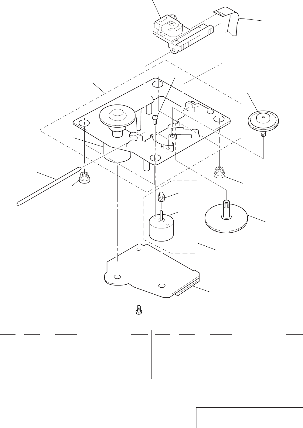
7-2. CD MECHANISM SECTION (CDM66-5BD27)
Ref. No. Part No. Description Remarks Ref. No. Part No. Description Remarks
101
110
110
110
111
102
113
M151
#1
111
103
115 117
105
106
107
a
a
108
109
104
BU-5BD27
not supplied
not
supplied
not
supplied
not
supplied
101 1-452-925-21 MAGNET ASSY
102 4-231-531-01 HOLDER (66)
103 4-231-530-01 TRAY (66)
104 1-541-632-11 MOTOR, DC (LOADING)
105 4-232-713-01 BELT (LD)
106 4-232-711-01 GEAR (LD)
107 4-232-710-01 PULLEY (LD)
108 4-232-712-01 CAM (66)
109 1-645-721-11 LOADING BOARD
110 4-227-899-01 SCREW (DIA. 12), FROATING
111 4-959-996-01 SPRING (932), COMPRESSION
113 4-231-529-01 CHASSIS (66)
115 4-993-142-03 PULLEY (L), PRESS
117 4-232-682-01 CUSHION (66)
M151 A-4604-363-A MOTOR (L) ASSY (LOADING)
25
CDP-XE570
7-3. BASE UNIT SECTION (BU-5BD27)
151
152
153
158
154
156
160
161
M102
M101
#2
157
159
155
154
not supplied
Ref. No. Part No. Description Remarks Ref. No. Part No. Description Remarks
0151 1-796-033-11 OPTICAL PICK UP
152 1-782-817-11 WIRE (FLAT TYPE) (16 CORE)
153 4-917-567-01 GEAR (M)
154 4-951-940-01 INSULATOR (BU)
155 4-917-565-01 SHAFT, SLED
156 4-917-564-01 GEAR (P), FLATNESS
157 A-4725-568-A BD BOARD,COMPLETE
158 3-713-786-51 SCREW +P 2X3
159 4-917-566-01 GEAR (S)
160 X-4917-504-1 MOTOR ASSY
161 X-4917-523-3 BASE (OUTSET) ASSY
M102 1-541-353-11 MOTOR (SLED)
The components identified by mark 0 or dotted
line with mark 0 are critical for safety.
Replace only with part number specified.

NOTE:
•Due to standardization, replacements in the
parts list may be different from the parts
specified in the diagrams or the components
used on the set.
•-XX, -X mean standardized parts, so they may
have some difference from the original one.
•Items marked “*” are not stocked since they
are seldom required for routine service. Some
delay should be anticipated when ordering these
items.
•CAPACITORS:
uF: µF
•RESISTORS
All resistors are in ohms.
METAL: metal-film resistor
METAL OXIDE: Metal Oxide-film resistor
F: nonflammable
•COILS
uH: µH The components identified by mark 0 or
dotted line with mark 0 are critical for safety.
Replace only with part number specified.
•SEMICONDUCTORS
In each case, u: µ, for example:
uA...: µA... , uPA... , µPA... ,
uPB... , µPB... , uPC... , µPC... ,
uPD..., µPD...
When indicating parts by reference number,
please include the board name.
Ref. No. Part No. Description Remarks Ref. No. Part No. Description Remarks
26
SECTION 8
ELECTRICAL PARTS LIST
CDP-XE570
A-4725-568-A BD BOARD,COMPLETE
******************
< CAPACITOR >
C101 1-164-315-11 CERAMIC CHIP 470PF 5.00% 50V
C102 1-164-156-11 CERAMIC CHIP 0.1uF 25V
C103 1-164-315-11 CERAMIC CHIP 470PF 5.00% 50V
C110 1-126-206-11 ELECT CHIP 100uF 20% 6.3V
C111 1-164-156-11 CERAMIC CHIP 0.1uF 25V
C112 1-164-156-11 CERAMIC CHIP 0.1uF 25V
C120 1-164-156-11 CERAMIC CHIP 0.1uF 25V
C121 1-162-970-11 CERAMIC CHIP 0.01uF 10% 25V
C122 1-117-863-11 CERAMIC CHIP 0.47uF 10.00% 6.3V
C123 1-162-927-11 CERAMIC CHIP 100PF 5% 50V
C124 1-162-967-11 CERAMIC CHIP 0.0033uF 10% 50V
C125 1-162-965-11 CERAMIC CHIP 0.0015uF 10% 50V
C126 1-107-826-11 CERAMIC CHIP 0.1uF 10.00% 16V
C130 1-164-505-11 CERAMIC CHIP 2.2uF 16V
C131 1-164-505-11 CERAMIC CHIP 2.2uF 16V
C132 1-164-505-11 CERAMIC CHIP 2.2uF 16V
C133 1-126-607-11 ELECT CHIP 47uF 20% 4V
C134 1-126-607-11 ELECT CHIP 47uF 20% 4V
C136 1-107-826-11 CERAMIC CHIP 0.1uF 10.00% 16V
C137 1-126-209-11 ELECT CHIP 100uF 20.00% 4V
C138 1-162-964-11 CERAMIC CHIP 0.001uF 10% 50V
C139 1-162-921-11 CERAMIC CHIP 33PF 5% 50V
C140 1-164-505-11 CERAMIC CHIP 2.2uF 16V
C145 1-162-908-11 CERAMIC CHIP 3PF 0.25PF 50V
C150 1-126-204-11 ELECT CHIP 47uF 20% 16V
C151 1-164-156-11 CERAMIC CHIP 0.1uF 25V
C152 1-162-919-11 CERAMIC CHIP 22PF 5% 50V
C153 1-162-919-11 CERAMIC CHIP 22PF 5% 50V
C154 1-162-964-11 CERAMIC CHIP 0.001uF 10% 50V
C158 1-164-172-11 CERAMIC CHIP 0.0056uF 10.00% 25V
C171 1-126-206-11 ELECT CHIP 100uF 20% 6.3V
C172 1-164-156-11 CERAMIC CHIP 0.1uF 25V
C173 1-162-928-11 CERAMIC CHIP 120PF 5% 50V
C174 1-115-412-11 CERAMIC CHIP 680PF 5.00% 25V
C181 1-126-206-11 ELECT CHIP 100uF 20% 6.3V
C182 1-164-156-11 CERAMIC CHIP 0.1uF 25V
C183 1-162-928-11 CERAMIC CHIP 120PF 5% 50V
C184 1-115-412-11 CERAMIC CHIP 680PF 5.00% 25V
C191 1-126-205-11 ELECT CHIP 47uF 20% 6.3V
C192 1-164-156-11 CERAMIC CHIP 0.1uF 25V
C193 1-162-920-11 CERAMIC CHIP 27PF 5% 50V
C194 1-162-918-11 CERAMIC CHIP 18PF 5.00% 50V
C199 1-164-156-11 CERAMIC CHIP 0.1uF 25V
< CONNECTOR >
CN101 1-784-360-11 CONNECTOR,FFC(LIF(NON-ZIF))21P
CN102 1-777-937-11 CONNECTOR, FFC/FPC 16P
< FERRITE BEAD >
FB191 1-216-864-11 METAL CHIP 0 5% 1/16W
< IC >
IC101 8-752-386-85 IC CXD2587Q
IC131 8-752-089-74 IC CXA2581N-T4
IC150 8-759-829-14 IC AN4800SB
< TRANSISTOR >
Q131 8-729-010-08 TRANSISTOR MSB710-RT1
Q132 8-729-600-22 TRANSISTOR 2SA1235TP-1EF
< RESISTOR >
R101 1-216-835-11 METAL CHIP 15K 5% 1/16W
R102 1-216-845-11 METAL CHIP 100K 5% 1/16W
R103 1-216-835-11 METAL CHIP 15K 5% 1/16W
R110 1-216-821-11 METAL CHIP 1K 5% 1/16W
R111 1-216-809-11 METAL CHIP 100 5% 1/16W
R112 1-216-833-11 METAL CHIP 10K 5% 1/16W
R120 1-216-839-11 METAL CHIP 33K 5% 1/16W
R121 1-216-833-11 METAL CHIP 10K 5% 1/16W
R122 1-216-845-11 METAL CHIP 100K 5% 1/16W
R123 1-216-857-11 METAL CHIP 1M 5% 1/16W
R125 1-216-827-11 METAL CHIP 3.3K 5% 1/16W
R126 1-216-833-11 METAL CHIP 10K 5% 1/16W
R127 1-216-821-11 METAL CHIP 1K 5% 1/16W
R129 1-216-815-11 METAL CHIP 330 5% 1/16W
R134 1-216-853-11 METAL CHIP 470K 5% 1/16W
R135 1-216-836-11 METAL CHIP 18K 5% 1/16W
R136 1-216-836-11 METAL CHIP 18K 5% 1/16W
R137 1-216-797-11 METAL CHIP 10 5% 1/16W
R138 1-216-798-11 RES-CHIP 12 5% 1/16W
R139 1-216-847-11 METAL CHIP 150K 5% 1/16W
R140 1-216-854-11 METAL CHIP 560K 5% 1/16W
R141 1-216-840-11 METAL CHIP 39K 5% 1/16W
R142 1-216-841-11 METAL CHIP 47K 5% 1/16W
R143 1-216-855-11 METAL CHIP 680K 5% 1/16W
R144 1-216-846-11 METAL CHIP 120K 5% 1/16W
R145 1-216-830-11 METAL CHIP 5.6K 5% 1/16W
R146 1-216-845-11 METAL CHIP 100K 5% 1/16W
R149 1-216-821-11 METAL CHIP 1K 5% 1/16W
R151 1-216-845-11 METAL CHIP 100K 5% 1/16W
R152 1-216-833-11 METAL CHIP 10K 5% 1/16W
BD

Ref. No. Part No. Description Remarks Ref. No. Part No. Description Remarks
27
CDP-XE570
R153 1-216-864-11 METAL CHIP 0 5% 1/16W
R155 1-216-836-11 METAL CHIP 18K 5% 1/16W
R171 1-218-720-11 METAL CHIP 15K 0.5% 1/16W
R172 1-218-720-11 METAL CHIP 15K 0.5% 1/16W
R173 1-218-720-11 METAL CHIP 15K 0.5% 1/16W
R174 1-216-809-11 METAL CHIP 100 5% 1/16W
R181 1-218-720-11 METAL CHIP 15K 0.5% 1/16W
R182 1-218-720-11 METAL CHIP 15K 0.5% 1/16W
R183 1-218-720-11 METAL CHIP 15K 0.5% 1/16W
R184 1-216-809-11 METAL CHIP 100 5% 1/16W
R191 1-216-817-11 METAL CHIP 470 5% 1/16W
R192 1-216-797-11 METAL CHIP 10 5% 1/16W
< COMPOSITION CIRCUIT BLOCK >
RB101 1-233-576-11 RES, CHIP NETWORK 100
RB102 1-233-576-11 RES, CHIP NETWORK 100
< SWITCH >
S101 1-572-085-11 SWITCH, LEAF(LIMIT)
< VIBRATOR >
X191 1-767-408-21 VIBRATOR, CRYSTAL 16.9344MHz
************************************************************
A-4725-621-A DISPLAY BOARD,COMPLETE
***********************
*4-929-709-31 GUIDE (FL TUBE)
< CAPACITOR >
C502 1-164-159-11 CERAMIC 0.1uF 50V
C503 1-126-382-11 ELECT 100uF 20.00% 10V
C505 1-164-159-11 CERAMIC 0.1uF 50V
C506 1-164-159-11 CERAMIC 0.1uF 50V
< CONNECTOR >
CN501 1-784-780-11 CONNECTOR, FFC 19P
< FILTER >
FL501 1-517-740-11 INDICATOR TUBE, FLUORESCENT
< IC >
IC501 8-752-921-33 IC CXP82832-033Q
IC502 8-759-459-86 IC NJL64H400A(REMOTE SENSOR)
< TRANSISTOR >
Q501 8-729-029-66 TRANSISTOR DTC114ESA-TP
Q502 8-729-029-66 TRANSISTOR DTC114ESA-TP
< RESISTOR >
R501 1-249-427-11 CARBON 6.8K 5% 1/4W F
R502 1-249-415-11 CARBON 680 5% 1/4W F
R503 1-249-417-11 CARBON 1K 5% 1/4W F
R504 1-249-419-11 CARBON 1.5K 5% 1/4W F
R505 1-249-421-11 CARBON 2.2K 5% 1/4W F
R511 1-249-427-11 CARBON 6.8K 5% 1/4W F
R512 1-249-415-11 CARBON 680 5% 1/4W F
R513 1-249-417-11 CARBON 1K 5% 1/4W F
R514 1-249-419-11 CARBON 1.5K 5% 1/4W F
R521 1-249-427-11 CARBON 6.8K 5% 1/4W F
R531 1-249-441-11 CARBON 100K 5% 1/4W
R532 1-249-441-11 CARBON 100K 5% 1/4W
R535 1-249-427-11 CARBON 6.8K 5% 1/4W F
R536 1-249-427-11 CARBON 6.8K 5% 1/4W F
R537 1-249-429-11 CARBON 10K 5% 1/4W
R539 1-249-429-11 CARBON 10K 5% 1/4W
R541 1-247-807-31 CARBON 100 5% 1/4W
R542 1-247-807-31 CARBON 100 5% 1/4W
R551 1-249-415-11 CARBON 680 5% 1/4W F
R552 1-249-417-11 CARBON 1K 5% 1/4W F
< SWITCH >
S501 1-771-349-21 SWITCH, KEYBOARD(x)
S502 1-771-349-21 SWITCH, KEYBOARD(X)
S503 1-771-349-21 SWITCH, KEYBOARD(G)
S504 1-771-349-21 SWITCH, KEYBOARD(OPEN/CLOSE A)
S511 1-771-349-21 SWITCH, KEYBOARD(M)
S512 1-771-349-21 SWITCH, KEYBOARD(m)
S531 1-475-543-11 ENCODER, ROTARY(l AMS L)
< VIBRATOR >
X501 1-579-125-11 VIBRATOR, CERAMIC 8MHz
************************************************************
1-681-127-11 HEADPHONE BOARD
*****************
< CAPACITOR >
C402 1-162-291-31 CERAMIC 560PF 10.00% 50V
C403 1-162-291-31 CERAMIC 560PF 10.00% 50V
< JACK >
J401 1-770-307-11 JACK (LARGE TYPE)(PHONES)
< COIL >
L402 1-412-911-11 FERRITE 0uH
L403 1-412-911-11 FERRITE 0uH
************************************************************
1-681-125-11 KEY BOARD
**********
< RESISTOR >
R522 1-249-415-11 CARBON 680 5% 1/4W F
R523 1-249-417-11 CARBON 1K 5% 1/4W F
R524 1-249-419-11 CARBON 1.5K 5% 1/4W F
R525 1-249-421-11 CARBON 2.2K 5% 1/4W F
R526 1-247-843-11 CARBON 3.3K 5% 1/4W
R527 1-249-427-11 CARBON 6.8K 5% 1/4W F
R528 1-249-431-11 CARBON 15K 5% 1/4W
BD DISPLAY KEYHEADPHONE

Ref. No. Part No. Description Remarks Ref. No. Part No. Description Remarks
28
CDP-XE570
< SWITCH >
S521 1-771-349-21 SWITCH, KEYBOARD(TIME/TEXT)
S522 1-771-349-21 SWITCH, KEYBOARD(FADER)
S523 1-771-349-21 SWITCH, KEYBOARD(CLEAR)
S524 1-771-349-21 SWITCH, KEYBOARD(CHECK)
S525 1-771-349-21 SWITCH, KEYBOARD(PEAK SEARCH)
S526 1-771-349-21 SWITCH, KEYBOARD(TIME EDIT)
S527 1-771-349-21 SWITCH, KEYBOARD(PLAY MODE)
S528 1-771-349-21 SWITCH, KEYBOARD(REPEART)
************************************************************
1-645-721-21 LOADING BOARD
**************
< CONNECTOR >
CN151 1-568-943-11 PIN, CONNECTOR 5P
< SWITCH >
S271 1-572-086-11 SWITCH, LEAF(LOAD OUT)
S272 1-572-086-11 SWITCH, LEAF(LOAD IN)
************************************************************
A-4725-622-A MAIN BOARD,COMPLETE
********************
7-685-871-01 SCREW +BVTT 3X6 (S)
< CAPACITOR >
C601 1-128-547-11 ELECT 6800uF 20.00% 16V
C602 1-126-767-11 ELECT 1000uF 20.00% 16V
C603 1-128-576-11 ELECT 100uF 20.00% 63V
C604 1-161-494-00 CERAMIC 0.022uF 25V
C605 1-161-494-00 CERAMIC 0.022uF 25V
C606 1-164-159-11 CERAMIC 0.1uF 50V
C607 1-164-159-11 CERAMIC 0.1uF 50V
C608 1-126-934-11 ELECT 220uF 20.00% 10V
C609 1-161-494-00 CERAMIC 0.022uF 25V
C610 1-136-165-00 MYLAR 0.1uF 5.00% 50V
C612 1-161-494-00 CERAMIC 0.022uF 25V
C616 1-126-916-11 ELECT 1000uF 20.00% 6.3V
C618 1-126-933-11 ELECT 100uF 20.00% 16V
C619 1-126-767-11 ELECT 1000uF 20.00% 16V
0C620 1-113-924-11 CERAMIC 0.0047uF 20.00% 250V
C624 1-162-282-31 CERAMIC 100PF 10% 50V
C631 1-161-494-00 CERAMIC 0.022uF 25V
C641 1-126-964-11 ELECT 10uF 20.00% 50V
C642 1-126-935-11 ELECT 470uF 20.00% 10V
C651 1-126-935-11 ELECT 470uF 20.00% 10V
C653 1-104-666-11 ELECT 220uF 20.00% 25V
C654 1-164-159-11 CERAMIC 0.1uF 50V
C657 1-164-159-11 CERAMIC 0.1uF 50V
C658 1-164-159-11 CERAMIC 0.1uF 50V
C659 1-161-494-00 CERAMIC 0.022uF 25V
C661 1-162-290-31 CERAMIC 470PF 10% 50V
C662 1-162-290-31 CERAMIC 470PF 10% 50V
C663 1-162-290-31 CERAMIC 470PF 10% 50V
C675 1-161-494-00 CERAMIC 0.022uF 25V
C677 1-161-494-00 CERAMIC 0.022uF 25V
C678 1-126-024-11 ELECT 220uF 20.00% 25V
C679 1-126-024-11 ELECT 220uF 20.00% 25V
C682 1-126-963-11 ELECT 4.7uF 20.00% 50V
C685 1-161-494-00 CERAMIC 0.022uF 25V
C695 1-161-494-00 CERAMIC 0.022uF 25V
C802 1-104-664-11 ELECT 47uF 20.00% 10V
C806 1-106-359-00 MYLAR 4700PF 5% 200V
C807 1-130-472-00 MYLAR 0.0012uF 5% 50V
C808 1-126-024-11 ELECT 220uF 20.00% 25V
C810 1-136-802-11 MYLAR 0.015uF 5.00% 100V
C811 1-136-808-11 FILM 100PF 5.00% 100V
C902 1-104-664-11 ELECT 47uF 20.00% 10V
C906 1-106-359-00 MYLAR 4700PF 5% 200V
C907 1-130-472-00 MYLAR 0.0012uF 5% 50V
C908 1-126-024-11 ELECT 220uF 20.00% 25V
C910 1-136-802-11 MYLAR 0.015uF 5.00% 100V
C911 1-136-808-11 FILM 100PF 5.00% 100V
< CONNECTOR >
CN621 1-784-780-11 CONNECTOR, FFC 19P
CN651 1-568-838-11 CONNECTOR, FFC 21P
CN681 1-506-468-11 PIN, CONNECTOR 3P
< DIODE >
D601 8-719-024-99 DIODE 11ES2-NTA2B
D602 8-719-024-99 DIODE 11ES2-NTA2B
D603 8-719-024-99 DIODE 11ES2-NTA2B
D604 8-719-024-99 DIODE 11ES2-NTA2B
D605 8-719-024-99 DIODE 11ES2-NTA2B
D612 8-719-024-99 DIODE 11ES2-NTA2B
D613 8-719-024-99 DIODE 11ES2-NTA2B
D614 8-719-109-85 DIODE MTZJ-T-72-5.1B
D615 8-719-911-19 DIODE 1SS133T-72
D616 8-719-911-19 DIODE 1SS133T-72
D621 8-719-911-19 DIODE 1SS133T-72
D631 8-719-983-63 DIODE MTZJ-T-72-3.3B
D641 8-719-983-84 DIODE MTZJ-T-72-30D
D643 8-719-109-85 DIODE MTZJ-T-72-5.1B
D681 8-719-911-19 DIODE 1SS133T-72
D682 8-719-911-19 DIODE 1SS133T-72
D691 8-719-911-19 DIODE 1SS133T-72
D692 8-719-911-19 DIODE 1SS133T-72
< IC >
IC601 8-759-039-69 IC uPC7805AHF
IC602 8-749-011-78 IC BA17807T
IC603 8-759-165-81 IC PST600D-T
IC631 8-759-598-69 IC BA6956AN
IC651 8-749-921-12 IC GP1F32T(DIGITAL OUT OPTICAL)
IC671 8-759-604-86 IC M5F7807L
IC672 8-759-604-90 IC M5F7907L
IC681 8-759-167-88 IC NJM4565D
IC801 8-759-710-59 IC NJM4580D-D
IC901 8-759-710-59 IC NJM4580D-D
The components identified by mark 0 or dotted
line with mark 0 are critical for safety.
Replace only with part number specified.
KEY LOADING MAIN

Ref. No. Part No. Description Remarks Ref. No. Part No. Description Remarks
29
CDP-XE570
< JACK >
J621 1-779-655-21 JACK (SMALL TYPE) (2 GANG)(CONTROL A1II)
J681 1-785-868-11 JACK, PIN 2P(ANALOG OUT)
< COIL >
L651 1-414-151-11 INDUCTOR 470uH
< TRANSISTOR >
Q621 8-729-119-78 TRANSISTOR 2SC1740S-QRT
Q642 8-729-041-38 TRANSISTOR 2SB1241TV2Q
Q681 8-729-029-56 TRANSISTOR DTA144ESA-TP
Q682 8-729-922-37 TRANSISTOR 2SD2144S-TP-UVW
Q683 8-729-922-37 TRANSISTOR 2SD2144S-TP-UVW
Q691 8-729-029-56 TRANSISTOR DTA144ESA-TP
Q692 8-729-922-37 TRANSISTOR 2SD2144S-TP-UVW
Q693 8-729-922-37 TRANSISTOR 2SD2144S-TP-UVW
< RESISTOR >
R611 1-249-429-11 CARBON 10K 5% 1/4W
R612 1-249-411-11 CARBON 330 5% 1/4W
R624 1-249-393-11 CARBON 10 5% 1/4W F
R625 1-249-429-11 CARBON 10K 5% 1/4W
R626 1-249-425-11 CARBON 4.7K 5% 1/4W F
R631 1-249-427-11 CARBON 6.8K 5% 1/4W F
R632 1-215-421-00 METAL 1K 1% 1/4W
R641 1-249-432-11 CARBON 18K 5% 1/4W
R642 1-249-432-11 CARBON 18K 5% 1/4W
R646 1-249-432-11 CARBON 18K 5% 1/4W
R647 1-247-807-31 CARBON 100 5% 1/4W
R648 1-247-807-31 CARBON 100 5% 1/4W
R651 1-247-807-31 CARBON 100 5% 1/4W
R652 1-247-807-31 CARBON 100 5% 1/4W
R653 1-247-807-31 CARBON 100 5% 1/4W
R681 1-249-441-11 CARBON 100K 5% 1/4W
R682 1-249-419-11 CARBON 1.5K 5% 1/4W F
R683 1-249-419-11 CARBON 1.5K 5% 1/4W F
R691 1-249-441-11 CARBON 100K 5% 1/4W
R692 1-249-419-11 CARBON 1.5K 5% 1/4W F
R693 1-249-419-11 CARBON 1.5K 5% 1/4W F
R804 1-215-445-00 METAL 10K 1% 1/4W
R805 1-249-429-11 CARBON 10K 5% 1/4W
R806 1-215-445-00 METAL 10K 1% 1/4W
R807 1-215-425-00 METAL 1.5K 1% 1/4W
R808 1-215-425-00 METAL 1.5K 1% 1/4W
R809 1-249-441-11 CARBON 100K 5% 1/4W
R810 1-249-414-11 CARBON 560 5% 1/4W F
R812 1-247-807-31 CARBON 100 5% 1/4W
R821 1-249-403-11 CARBON 68 5% 1/4W F
R904 1-215-445-00 METAL 10K 1% 1/4W
R905 1-249-429-11 CARBON 10K 5% 1/4W
R906 1-215-445-00 METAL 10K 1% 1/4W
R907 1-215-425-00 METAL 1.5K 1% 1/4W
R908 1-215-425-00 METAL 1.5K 1% 1/4W
R909 1-249-441-11 CARBON 100K 5% 1/4W
R910 1-249-414-11 CARBON 560 5% 1/4W F
R912 1-247-807-31 CARBON 100 5% 1/4W
R921 1-249-403-11 CARBON 68 5% 1/4W F
************************************************************
1-681-126-11 POWER SW BOARD
****************
< CAPACITOR >
0C621 1-113-924-11 CERAMIC 0.0047uF 20.00% 250V
< CONNECTOR >
*CN601 1-580-230-31 PIN, CONNECTOR (PC BOARD) 2P
CN602 1-564-321-00 PIN, CONNECTOR 2P
< SWITCH >
0S601 1-762-581-11 SWITCH, AC POWER PUSH (1 KEY) (POWER)
************************************************************
MISCELLANEOUS
**************
10 1-773-114-11 WIRE (FLAT TYPE) (19 CORE)
17 1-773-149-11 WIRE (FLAT TYPE) (21 CORE)
018 1-575-651-21 CORD, POWER
026 1-770-019-11 ADAPTOR, CONVERSION PLUG 3P (UK)
101 1-452-925-21 MAGNET ASSY
104 1-541-632-11 MOTOR, DC (LOADING)
0151 1-796-033-11 OPTICAL PICK UP (PXR-104X)
152 1-782-817-11 WIRE (FLAT TYPE) (16 CORE)
M102 1-541-353-11 MOTOR (SLED)
0T601 1-437-258-11 TRANSFORMER, POWER
************************************************************
ACCESSORIES & PACKING MATERIALS
*******************************
1-418-765-11 REMOTE COMMANDER (RM-DX740)
1-776-263-11 CORD, CONNECTION
4-233-601-11 MANUAL, INSTRUCTION (ENGLISH,FRENCH)(AEP)
4-233-601-21 MANUAL, INSTRUCTION (GERMAN,SPANISH,
DUTCH,SWEDISH,ITALIAN,POLISH)(AEP)
4-233-601-71 MANUAL, INSTRUCTION (ENGLISH)(UK)
4-983-956-01 COVER, BATTERY
************************************************************
The components identified by mark 0 or dotted
line with mark 0 are critical for safety.
Replace only with part number specified.
MAIN POWER SW
*************
HARDWARE LIST
*************
#1 7-621-775-10 SCREW +B 2.6X4
#2 4-951-620-01 SCREW (2.6X8), +BVTP