Sony Group BTMS2 Bluetooth Module User Manual CJ
Sony Corporation Bluetooth Module CJ
UserManual.wiki
>
Sony Group
>
BTMS2 User Manual
BTMS2_User manual_REV2
Navigation menu
Upload a User Manual
Namespaces
Wiki Guide
HTML
PDF
Info
Views
User Manual
Discussion / Help
Navigation
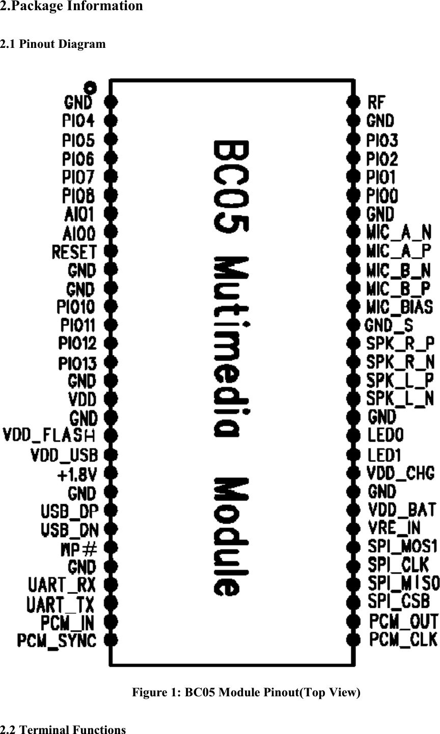
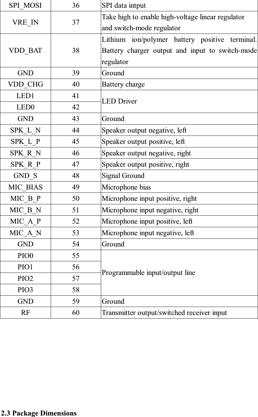
![Pin Name Pin Number DescriptionGND 1 GroundPIO4 2PIO5 3PIO6 4PIO7 5PIO8 6Programmable input/output lineAIO1 7AIO0 8 Analogue programmable input/outputRESET 9 System Reset(Low Active)GND 10 GroundGND 11 GroundPIO10 12PIO11 13PIO12 14PIO13 15Programmable input/output lineGND 16 GroundVDD 17 Positive supply for SPI/PCM ports and PIO[15:4]and BC05 MM Flash Pads, Connect to 3.3VGND 18 GroundVDD_Flash 19 Positive supply for Flash Memory ,Connect to 3.3VVDD_USB 20 Positive supply for UART/USB ports+1.8V 21 Switch-mode power regulator outputGND 22 GroundUSB_DP 23 USB data plus with selectable internal 1.5k pull-up resistorUSB_DN 24 USB data minusWP# 25 Flash write protect(Low Active)GND 26 GroundUART_RX 27 UART data inputUART_TX 28 UART data outputPCM_IN 29 Synchronous data inputPCM_SYNC 30 Synchronous data syncPCM_CLK 31 Synchronous data clockPCM_OUT 32 Synchronous data outputSPI_CSB 33 Chip select for SPI, active lowSPI_MOSO 34 SPI data outputSPI_CLK 35 SPI clock](https://usermanual.wiki/Sony-Group/BTMS2/User-Guide-1855385-Page-5.png)