Sony 6220511 Transmitter module for mobile applications User Manual
Sony Mobile Communications Inc Transmitter module for mobile applications
UserManual.wiki
>
Sony
>
6220511 User Manual
Integrators Manual
Navigation menu
Upload a User Manual
Namespaces
Wiki Guide
HTML
PDF
Info
Views
User Manual
Discussion / Help
Navigation
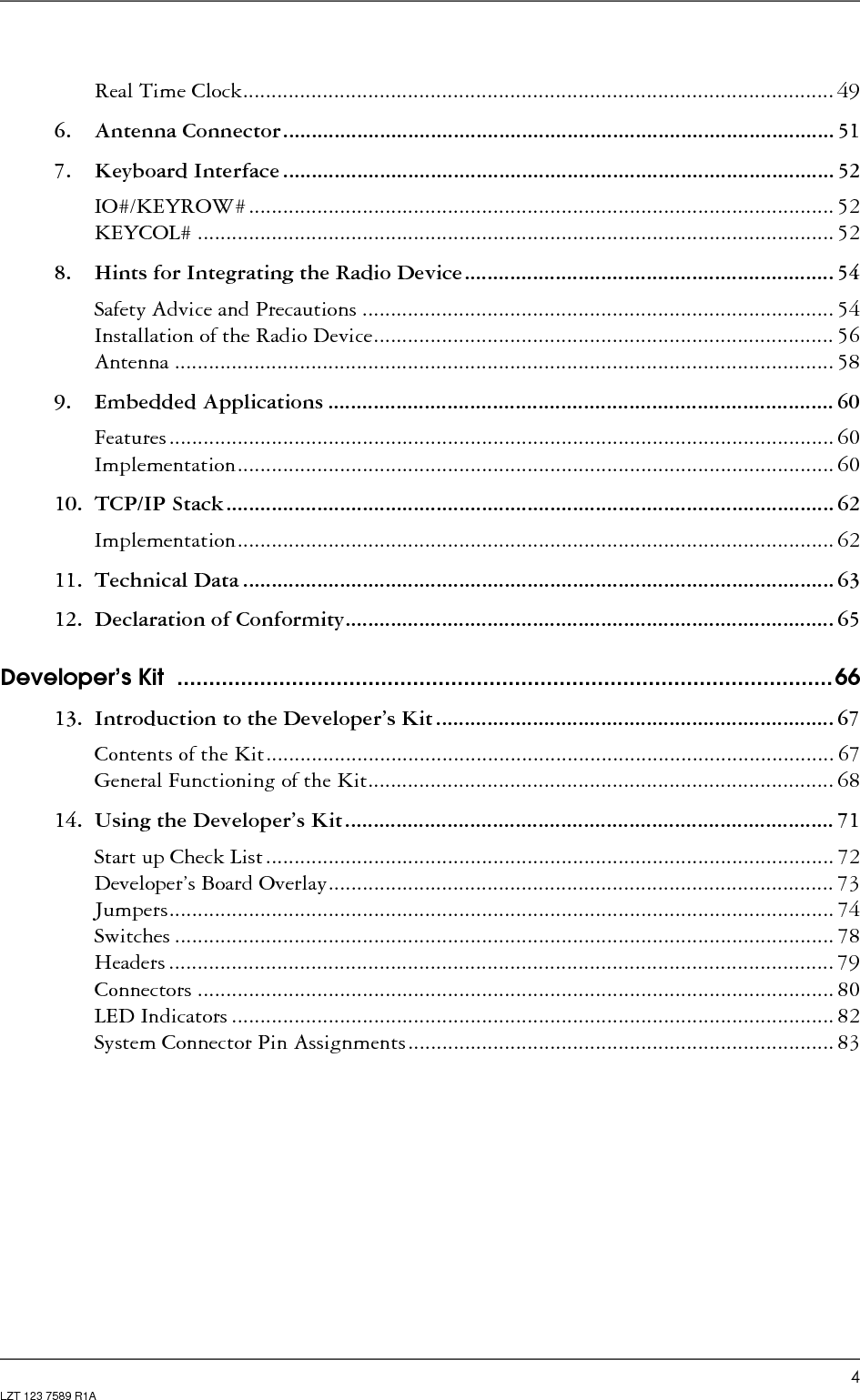
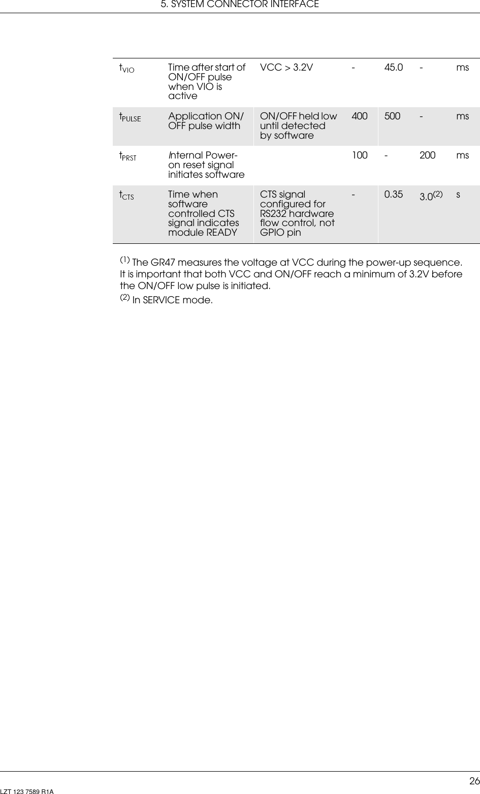
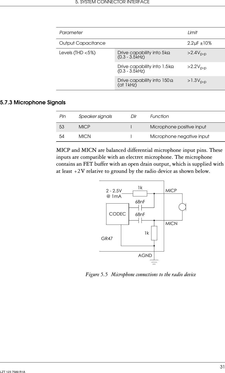
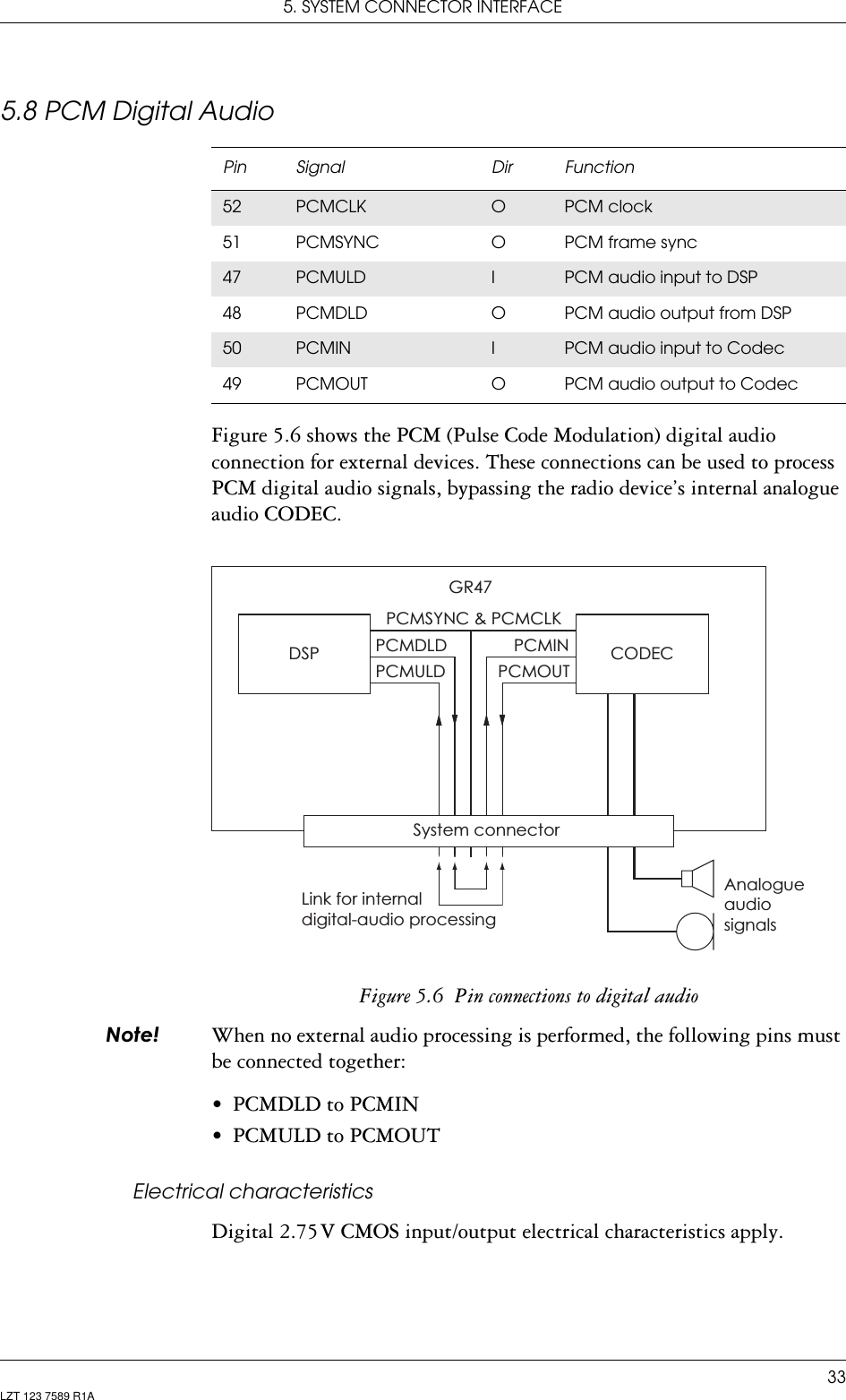
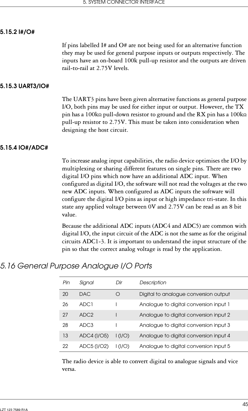
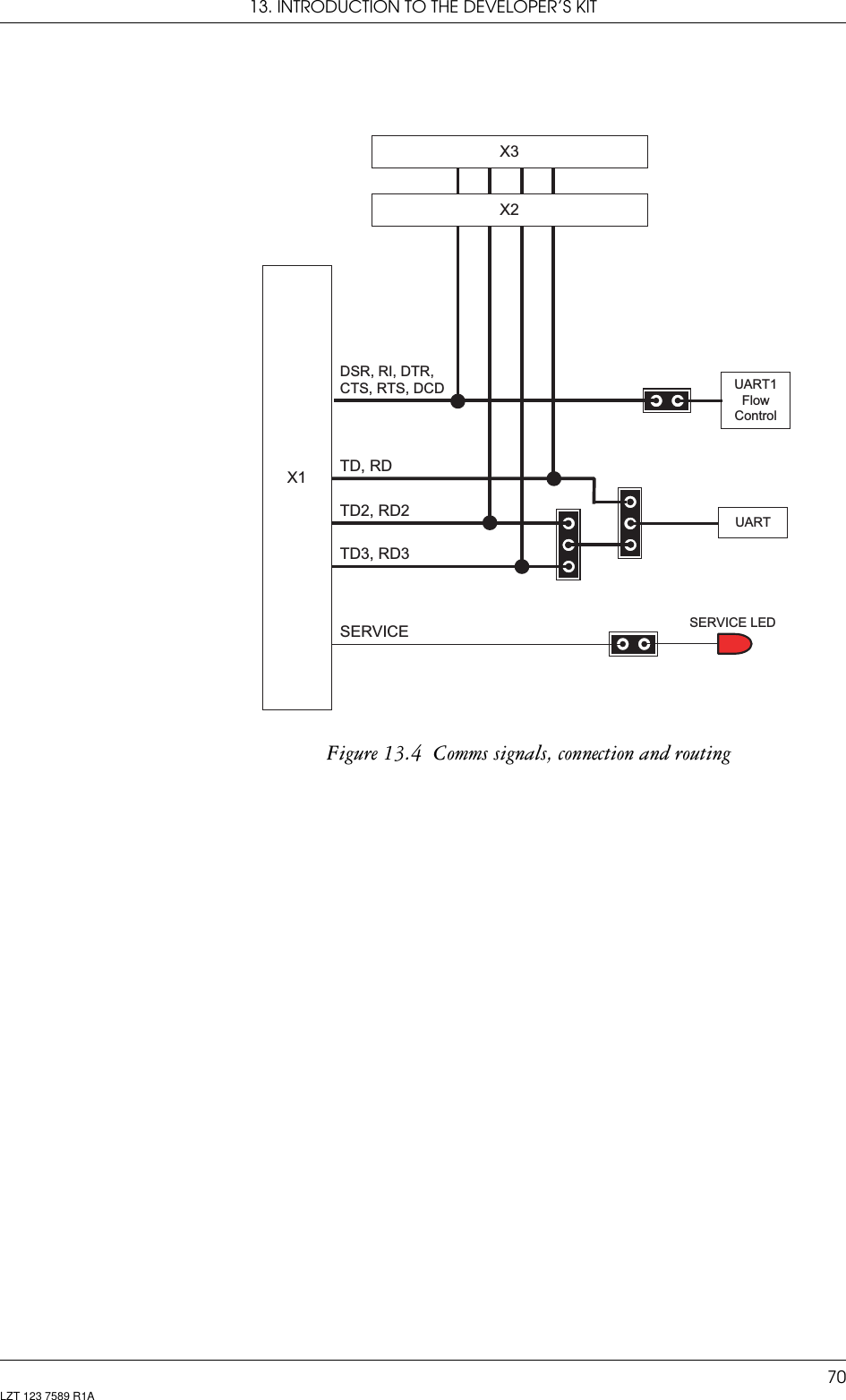
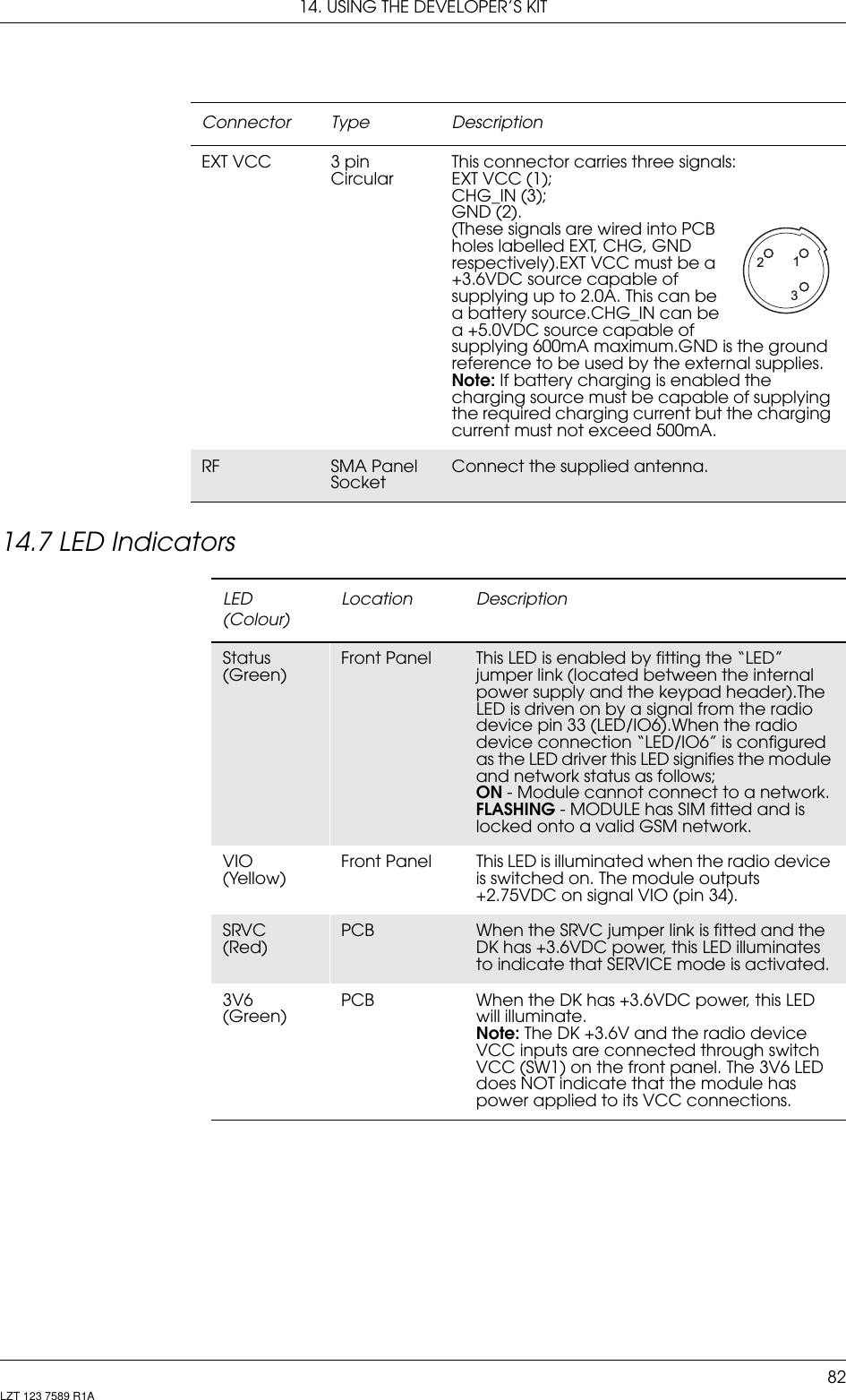
![5. SYSTEM CONNECTOR INTERFACE32LZT 123 7589 R1A5.7.4 Speaker SignalsBEARP and BEARN are the speaker output pins. These are differential-mode outputs. The electrical characteristics are given in the table below.(5) See PCMIN signal in 5.8 PCM Digital Audio, page 33.The following table shows the ear piece impedances that can be connected to BEARP and BEARN.Pin Speaker signals Dir Function55 BEARP OSpeaker positive output56 BEARN O Speaker negative outputParameter LimitOutput level (differential) ≥ 4.0 VOutput level (dynamic load = 32 Ω)≥ 2.8 VGain PCMIN(5) to BEARP/BEARN (differential) – 9 dB ± 1Distortion at 1 kHz and maximum output level ≤ 5 %Offset, BEARP to BEARN ± 30 mVEar-piece mute-switch attenuation ≥ 40 dBEar piece model Impedance ToleranceDynamic ear piece [32 Ω + 800 µH] // 100 pF ± 20 %Dynamic ear piece [150 Ω + 800 µH] // 100 pF ± 20 %Piezo ear piece 1 kΩ + 60 nF ± 20 %](https://usermanual.wiki/Sony/6220511/User-Guide-362096-Page-32.png)