Sony BC051021 Quadband GPRS Module User Manual MANUAL 119817 5FCP1013595 Uen
Sony Mobile Communications Inc Quadband GPRS Module MANUAL 119817 5FCP1013595 Uen
UserManual.wiki
>
Sony
>
BC051021 User Manual
Users Manual
Navigation menu
Upload a User Manual
Namespaces
Wiki Guide
HTML
PDF
Info
Views
User Manual
Discussion / Help
Navigation

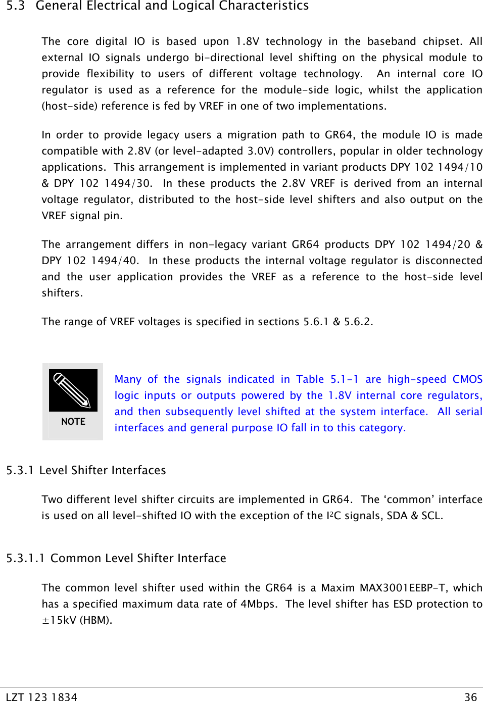
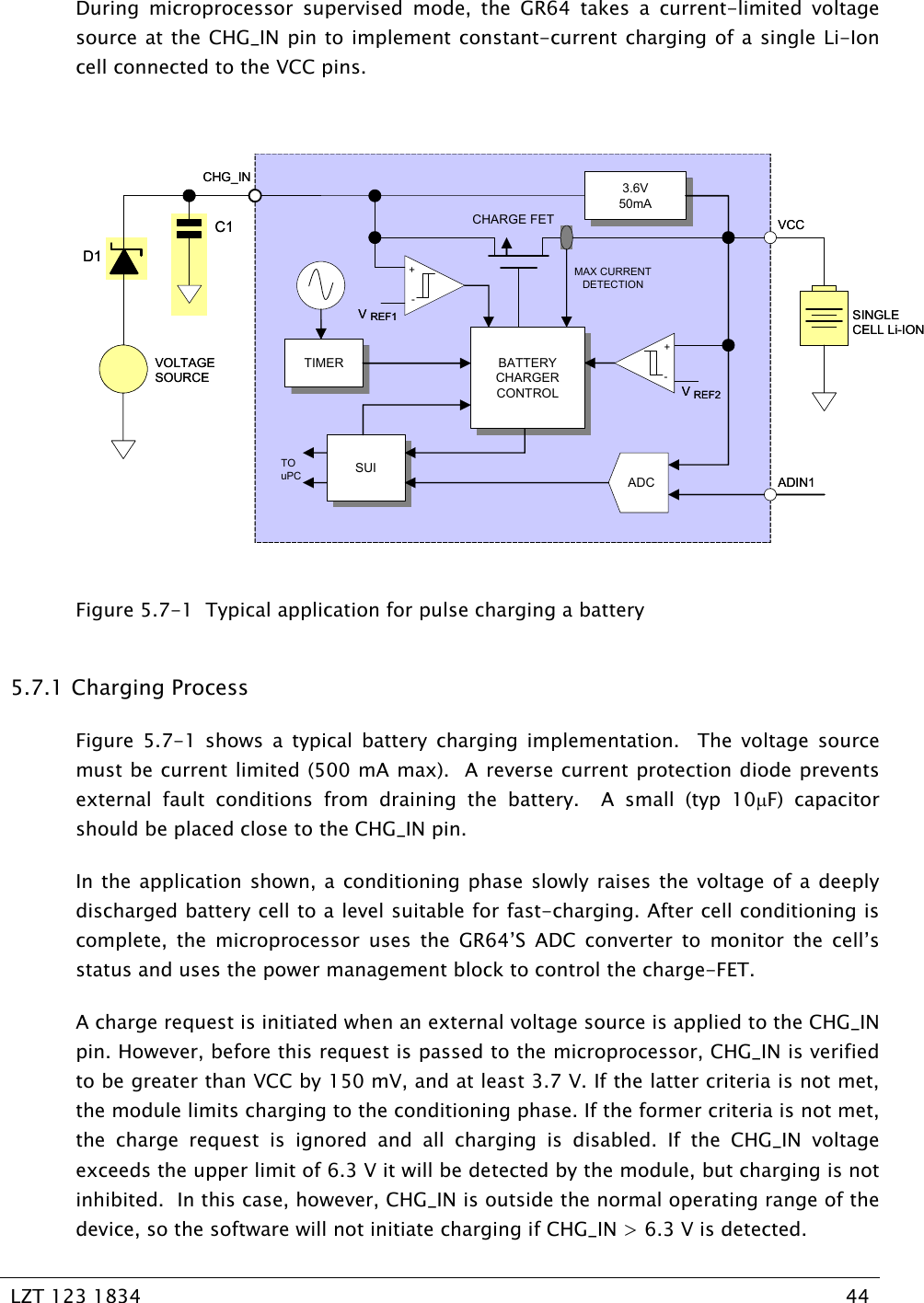
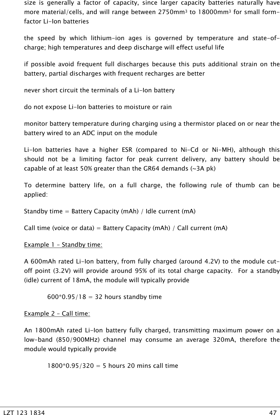
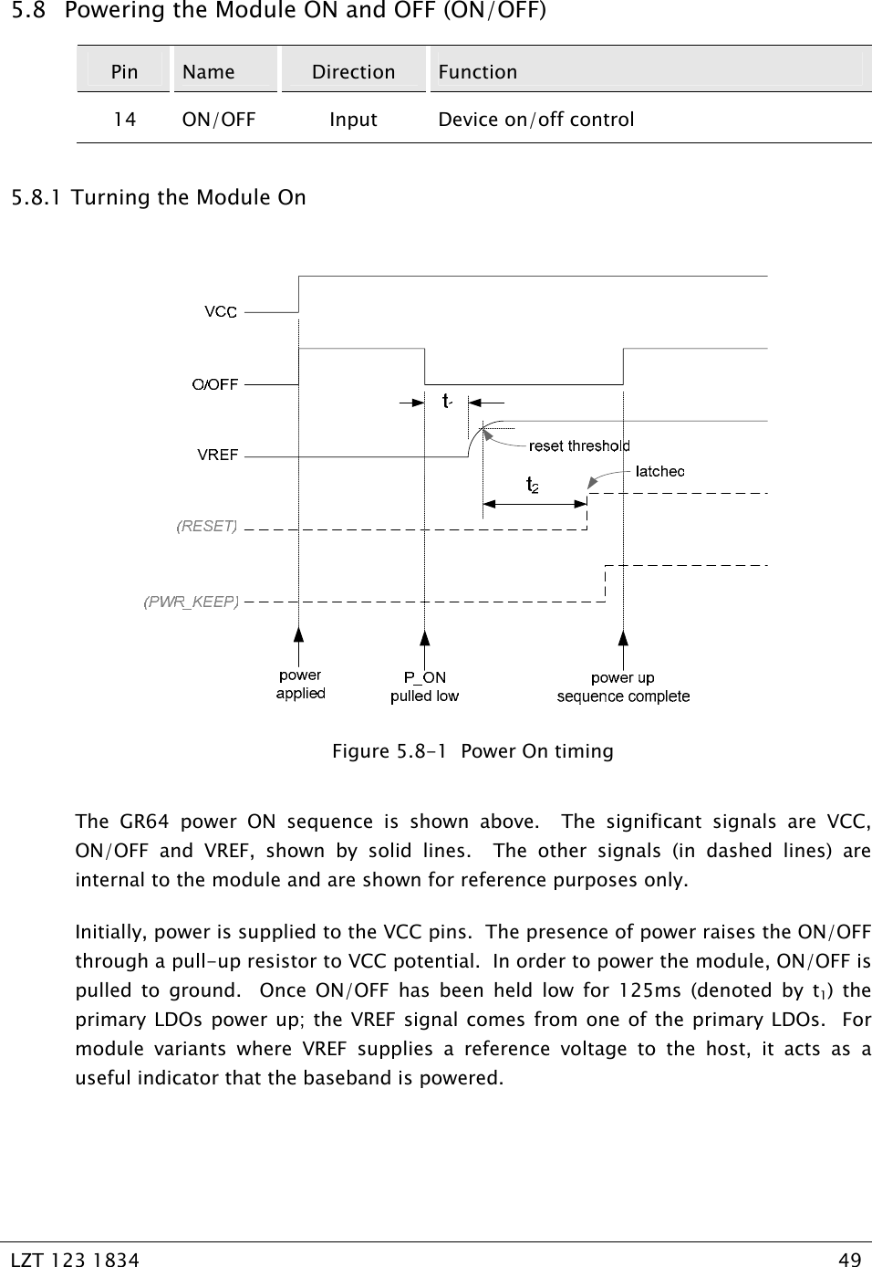
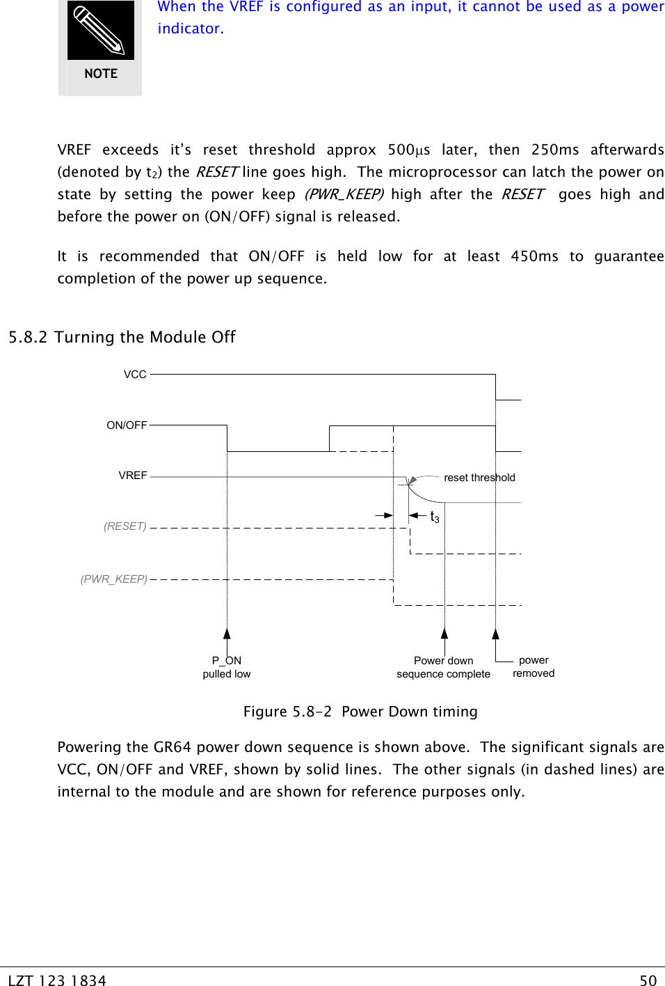
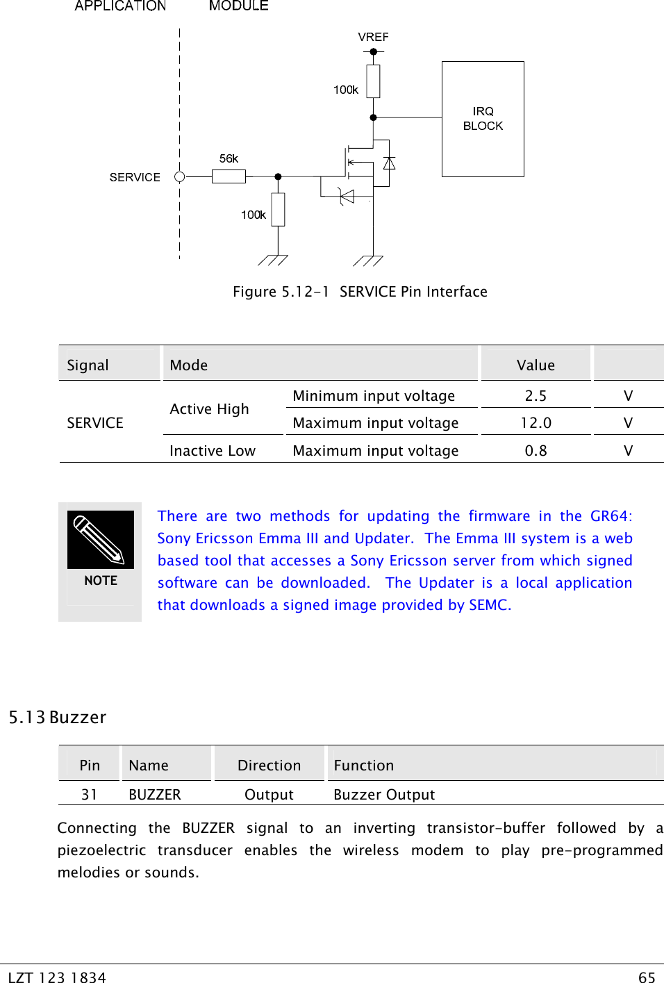
![LZT 123 1834 48 Example 3 – Typical Operation: A module performing periodic network data transfers and communicating intervallic status information to its host would spend its non-active periods in sleep mode. If the module spends 30 mins each day on call (320mA), 30 second each hour performing housekeeping, monitoring and status tasks (110mA), and sleeps (2.1mA) during the intervening periods, an 1800mAh rated Li-Ion battery fully charged would typically provide 1800*0.95/([0.5hr*320]+[0.2hr*110]+[23.3hr*2.1]) = 7 days 6 hrs operation The above examples are given for guidance, the actual battery life will depend upon variables such as battery condition, number of previous charge/discharge cycles, operating temperature, series resistance between battery and the module, and manufacturing tolerances CAUTION](https://usermanual.wiki/Sony/BC051021/User-Guide-660936-Page-48.png)