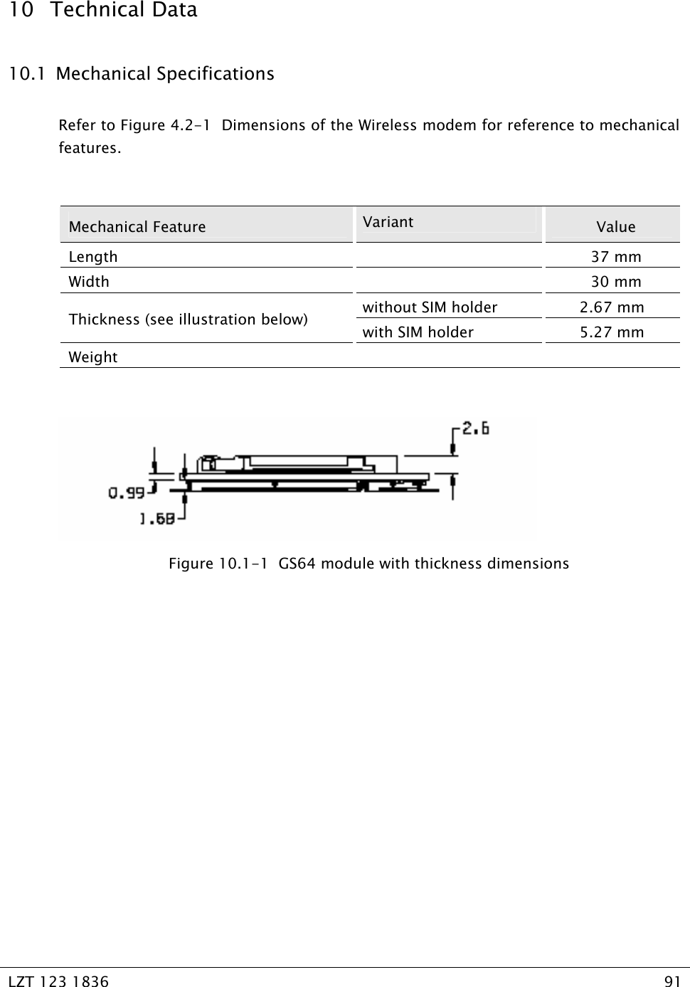
Sony BC051022 Quadband GPRS Module User Manual
Sony Mobile Communications Inc Quadband GPRS Module
UserManual.wiki
>
Sony
>
BC051022 User Manual
User Manual
Navigation menu
Upload a User Manual
Namespaces
Wiki Guide
HTML
PDF
Info
Views
User Manual
Discussion / Help
Navigation
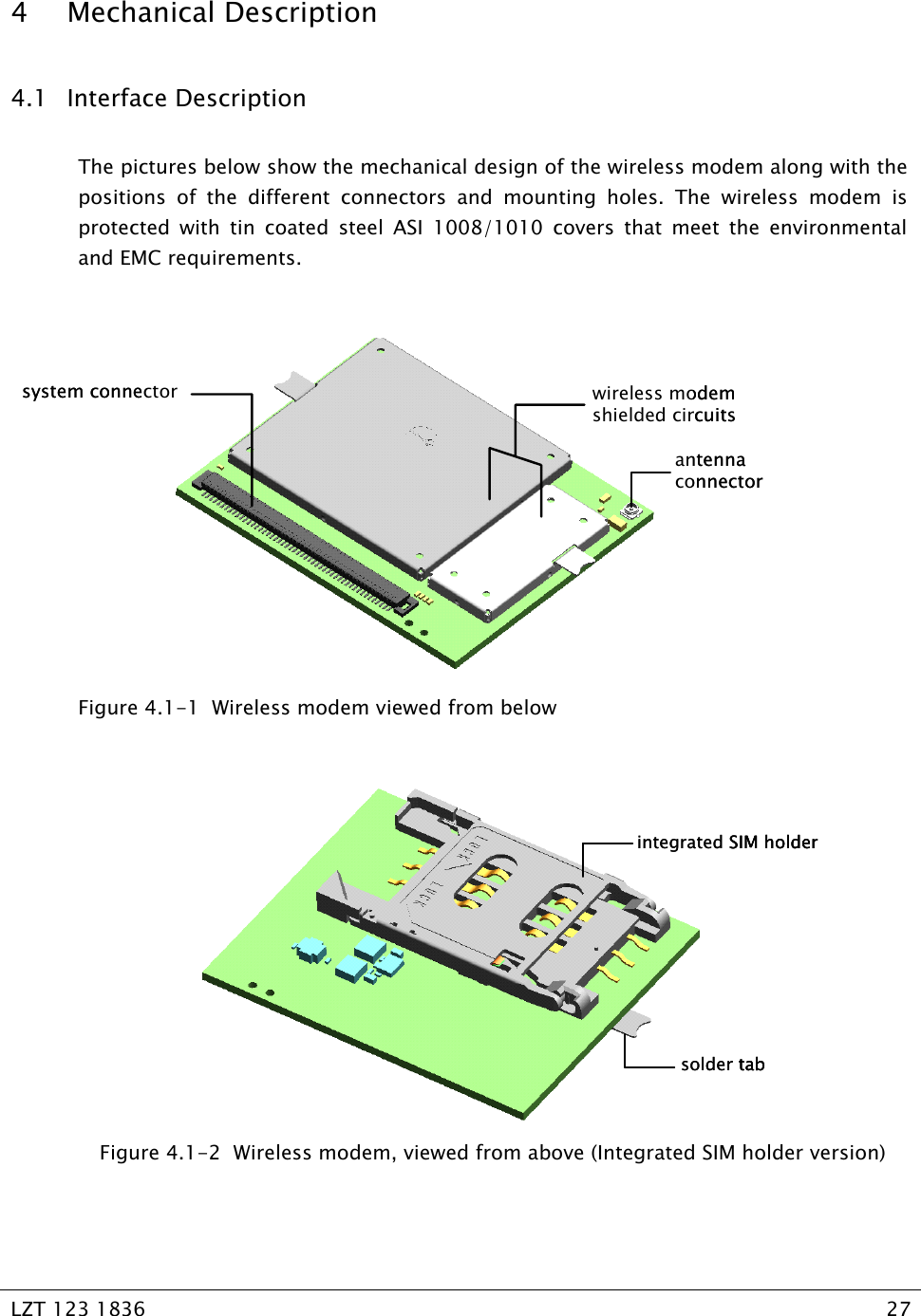
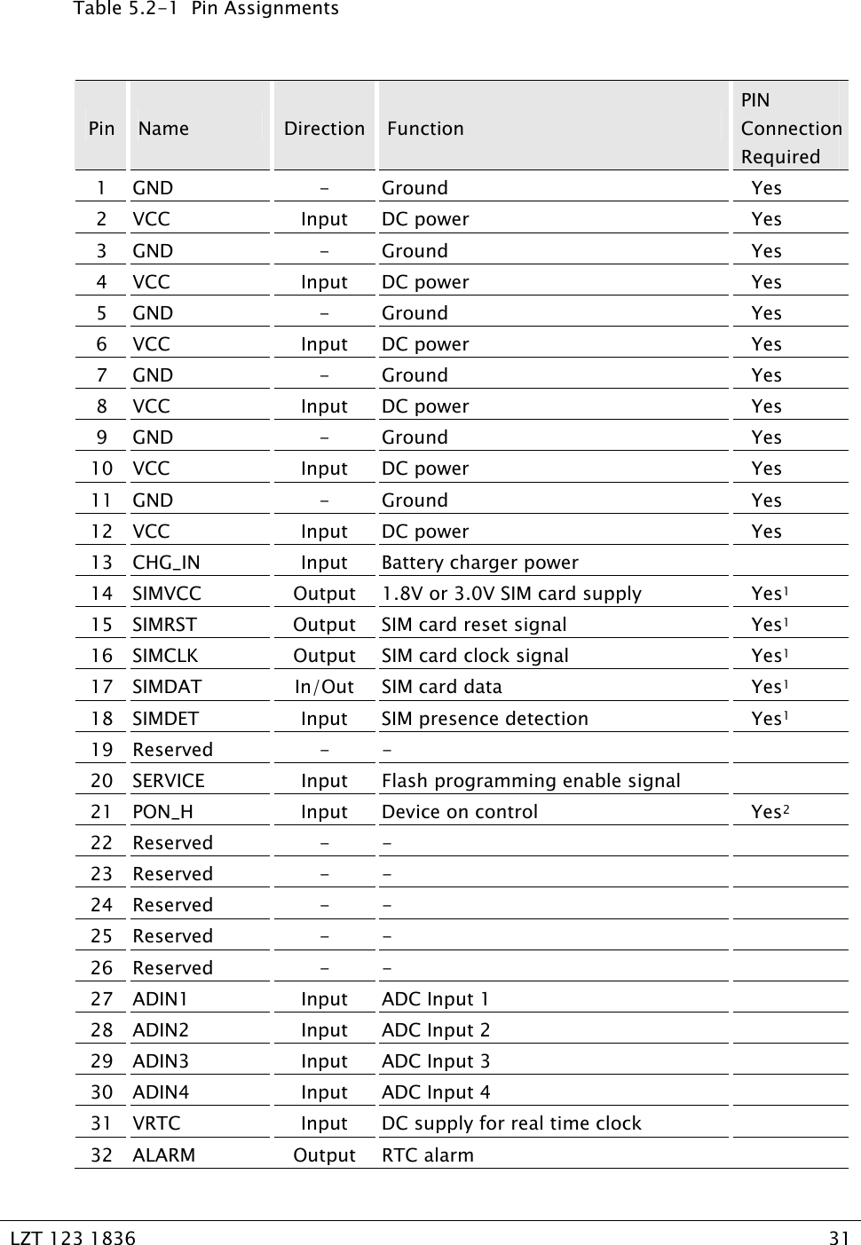
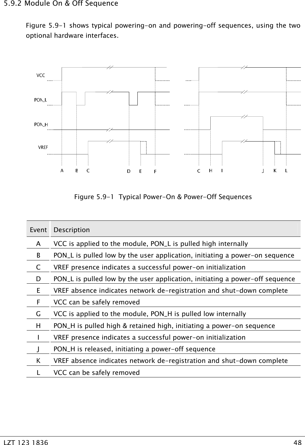
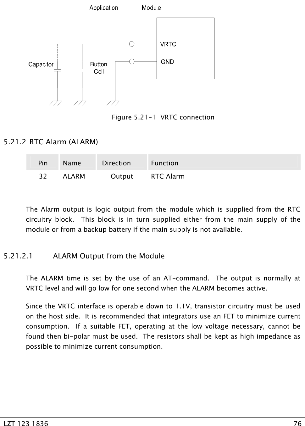
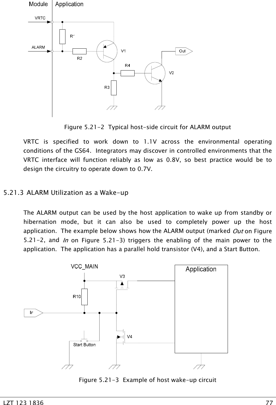
![LZT 123 1836 6 5.9.3 TURNING THE MODULE OFF .............................................................................. 50 5.10 ANALOGUE AUDIO................................................................................................ 52 5.10.1 AUXILIARY AUDIO TO MOBILE STATION (AUXIP, AUXIN)......................................53 5.10.2 AUXILIARY AUDIO FROM MOBILE STATION (AUXOP, AUXON) ..............................53 5.10.3 MICROPHONE SIGNALS (MICIP, MICIN) ...............................................................54 5.10.4 SPEAKER SIGNALS (EARP, EARN)......................................................................... 55 5.11 PCM DIGITAL AUDIO (SSP).....................................................................................55 5.11.1 PCM DATA FORMAT .......................................................................................... 55 5.12 SERIAL DATA INTERFACES.....................................................................................57 5.12.1 UART1 ..............................................................................................................57 5.12.2 SERIAL DATA SIGNALS (DTM1, DFM1)................................................................58 5.12.2.1 SERIAL DATA FROM WIRELESS MODEM (DFM1) ...............................................58 5.12.2.2 SERIAL DATA TO WIRELESS MODEM (DTM1)....................................................59 5.12.3 CONTROL SIGNALS (RTS1, CTS1, DTR1, DSR1, DCD1, RI)................................... 59 5.12.3.1 HARDWARE FLOW CONTROL RTS1 AND CTS1.................................................59 5.12.3.2 REQUEST TO SEND (RTS1).............................................................................. 59 5.12.3.3 CLEAR TO SEND (CTS1).................................................................................. 59 5.12.3.4 DATA TERMINAL READY (DTR1) .....................................................................60 5.12.3.5 DATA SET READY (DSR1) ...............................................................................60 5.12.3.6 DATA CARRIER DETECT (DCD1) .....................................................................60 5.12.3.7 RING INDICATOR (RI) ..................................................................................... 60 5.12.4 UART2 (DTM2, DFM2) ....................................................................................... 61 5.12.4.1 TRANSMITTED DATA (DTM2) .........................................................................61 5.12.4.2 RECEIVED DATA (DFM2)................................................................................. 61 5.12.4.3 REQUEST TO SEND (RTS2).............................................................................. 61 5.12.4.4 CLEAR TO SEND (CTS2).................................................................................. 61 5.12.5 USB...................................................................................................................62 5.12.6 SIM CARD INTERFACE........................................................................................63 5.12.7 SIM DETECTION (SIMDET)..................................................................................64 5.13 SYNCHRONOUS SERIAL PORT (SSP) INTERFACE [TO BE IMPLEMENTED IN A FUTURE RELEASE] 64 5.14 MEMORY CARD INTERFACE (SD/MMC) [TO BE IMPLEMENTED IN A FUTURE RELEASE] ..... 65 5.14.1 MULTIMEDIA CARD SYSTEM...............................................................................65 5.14.2 SECURE DIGITAL MEMORY CARD SYSTEM........................................................... 66 5.15 SERVICE/PROGRAMMING ......................................................................................67 5.16 LED [TO BE IMPLEMENTED IN A FUTURE RELEASE] ...............................................................67 5.17 GENERAL PURPOSE IO ...........................................................................................69](https://usermanual.wiki/Sony/BC051022/User-Guide-670126-Page-6.png)
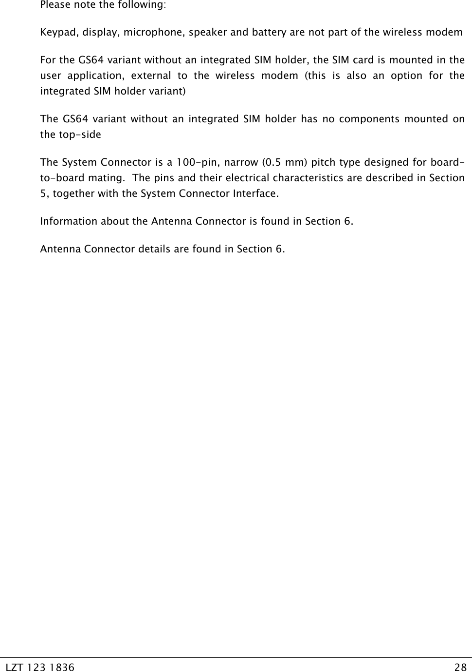
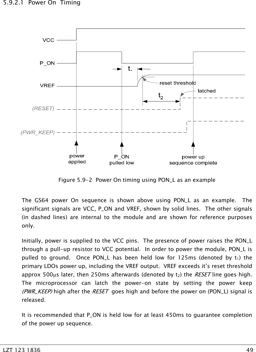
![LZT 123 1836 7 5.17.1 EMBEDDED APPLICATIONS................................................................................. 70 5.18 KEYBOARD SIGNALS (KEYROW, KEYCOL)................................................................ 72 5.19 ANALOGUE TO DIGITAL CONVERTERS (ADIN1, ADIN2, ADIN3, ADIN4) ...................72 5.20 BURST TRANSMISSION (TX_ON).............................................................................74 5.21 REAL TIME CLOCK ................................................................................................74 5.21.1 REAL TIME CLOCK BACKUP SUPPLY (VRTC).........................................................75 5.21.2 RTC ALARM (ALARM)......................................................................................... 76 5.21.2.1 ALARM OUTPUT FROM THE MODULE.............................................................. 76 5.21.3 ALARM UTILIZATION AS A WAKE-UP.................................................................. 77 5.22 RINGER OUTPUT (BUZZER) [TO BE IMPLEMENTED IN A FUTURE RELEASE]..............................78 6 Antenna Connector ............................................................................... 79 7 Hints for Integrating the Wireless Modem ............................................. 80 7.1 SAFETY ADVICE AND PRECAUTIONS .........................................................................80 7.1.1 GENERAL ..........................................................................................................80 7.2 SIM CARD ................................................................................................................81 7.3 ANTENNA ................................................................................................................81 7.4 INSTALLATION OF THE WIRELESS MODEM................................................................. 82 7.4.1 WHERE TO INSTALL THE WIRELESS MODEM ........................................................82 7.4.1.1 ENVIRONMENTAL CONDITIONS ...................................................................... 82 7.4.1.2 SIGNAL STRENGTH ........................................................................................83 7.4.1.3 CONNECTION OF COMPONENTS TO WIRELESS MODEM................................... 83 7.4.1.4 NETWORK AND SUBSCRIPTION.......................................................................83 7.4.2 HOW TO INSTALL THE WIRELESS MODEM ...........................................................84 7.4.2.1 POWER SUPPLY ..............................................................................................84 7.4.2.2 GROUNDS......................................................................................................84 7.4.2.3 AUDIO........................................................................................................... 84 7.4.2.4 SOFTWARE UPGRADE .....................................................................................85 7.5 ANTENNA ................................................................................................................85 7.5.1 GENERAL ..........................................................................................................85 7.5.2 ANTENNA TYPE.................................................................................................85 7.5.3 ANTENNA PLACEMENT ...................................................................................... 86 7.5.4 THE ANTENNA CABLE........................................................................................ 86](https://usermanual.wiki/Sony/BC051022/User-Guide-670126-Page-7.png)

![LZT 123 1836 46 Example 2 – Call time: An 1800mAh rated Li-Ion battery fully charged, transmitting maximum power on a low-band (850/900MHz) channel may consume an average 320mA, therefore the module would typically provide 1800*0.95/320 = 5 hours 20 mins call time Example 3 – Typical Operation: A module performing periodic network data transfers and communicating intervallic status information to its host would spend its non-active periods in sleep mode. If the module spends 30 mins each day on call (320mA), 30 second each hour performing housekeeping, monitoring and status tasks (110mA), and sleeps (2.1mA) during the intervening periods, an 1800mAh rated Li-Ion battery fully charged would typically provide 1800*0.95/([0.5hr*320]+[0.2hr*110]+[23.3hr*2.1]) = 7 days 6 hrs operation The above examples are given for guidance, the actual battery life will depend upon variables such as battery condition, number of previous charge/discharge cycles, operating temperature, series resistance between battery and the module, and manufacturing tolerances CAUTION](https://usermanual.wiki/Sony/BC051022/User-Guide-670126-Page-46.png)
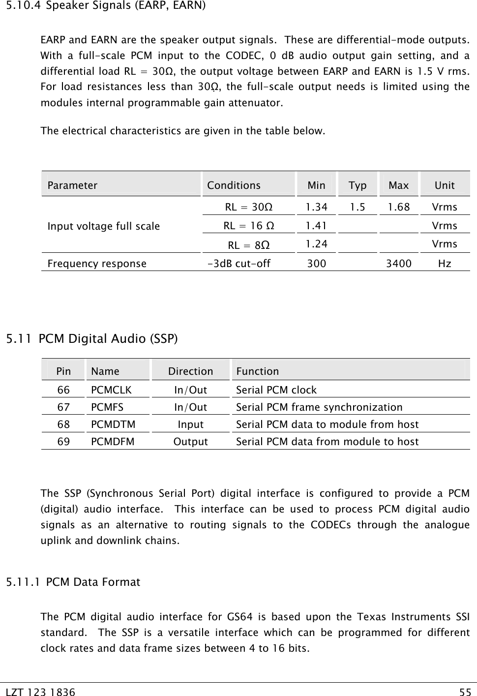
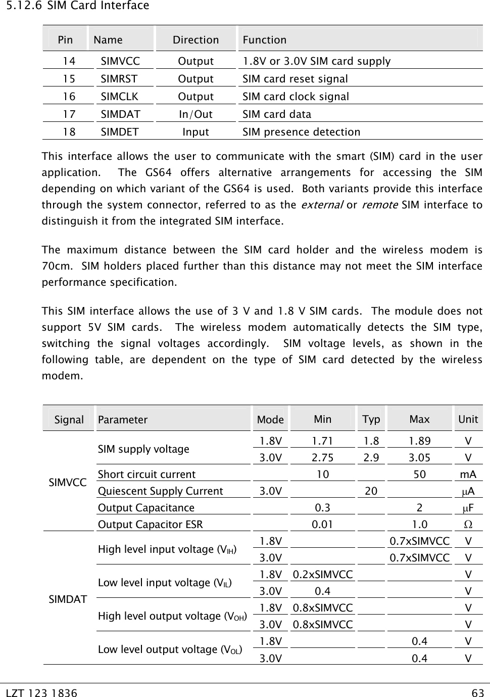
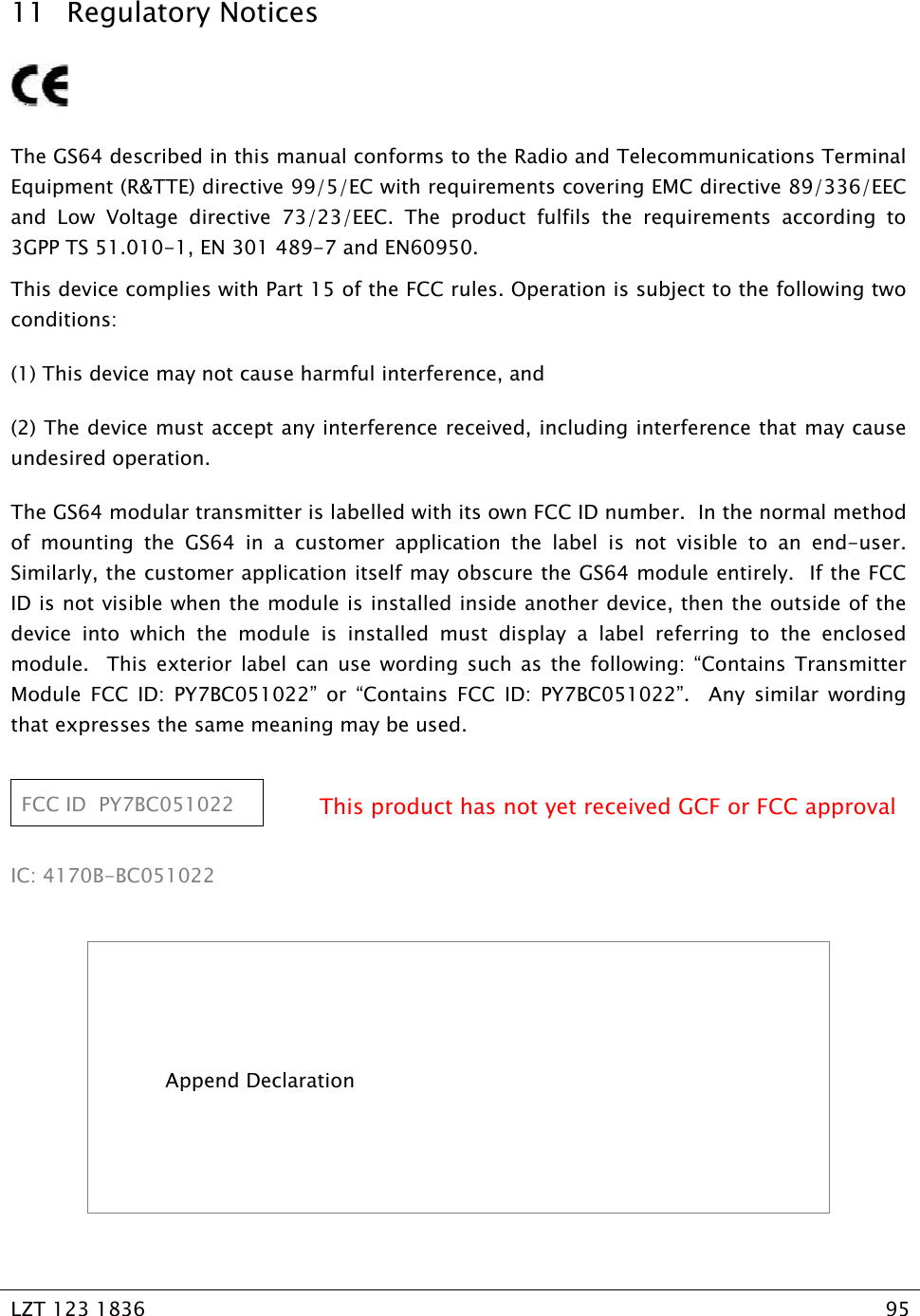
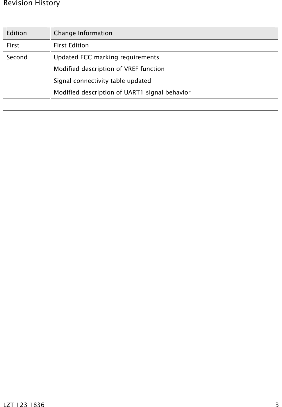
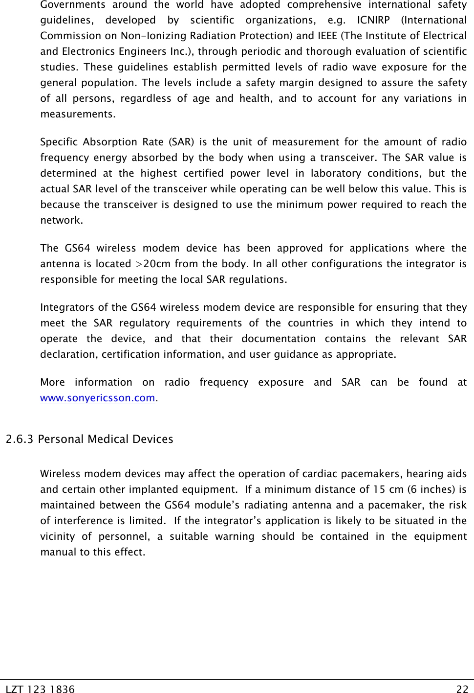
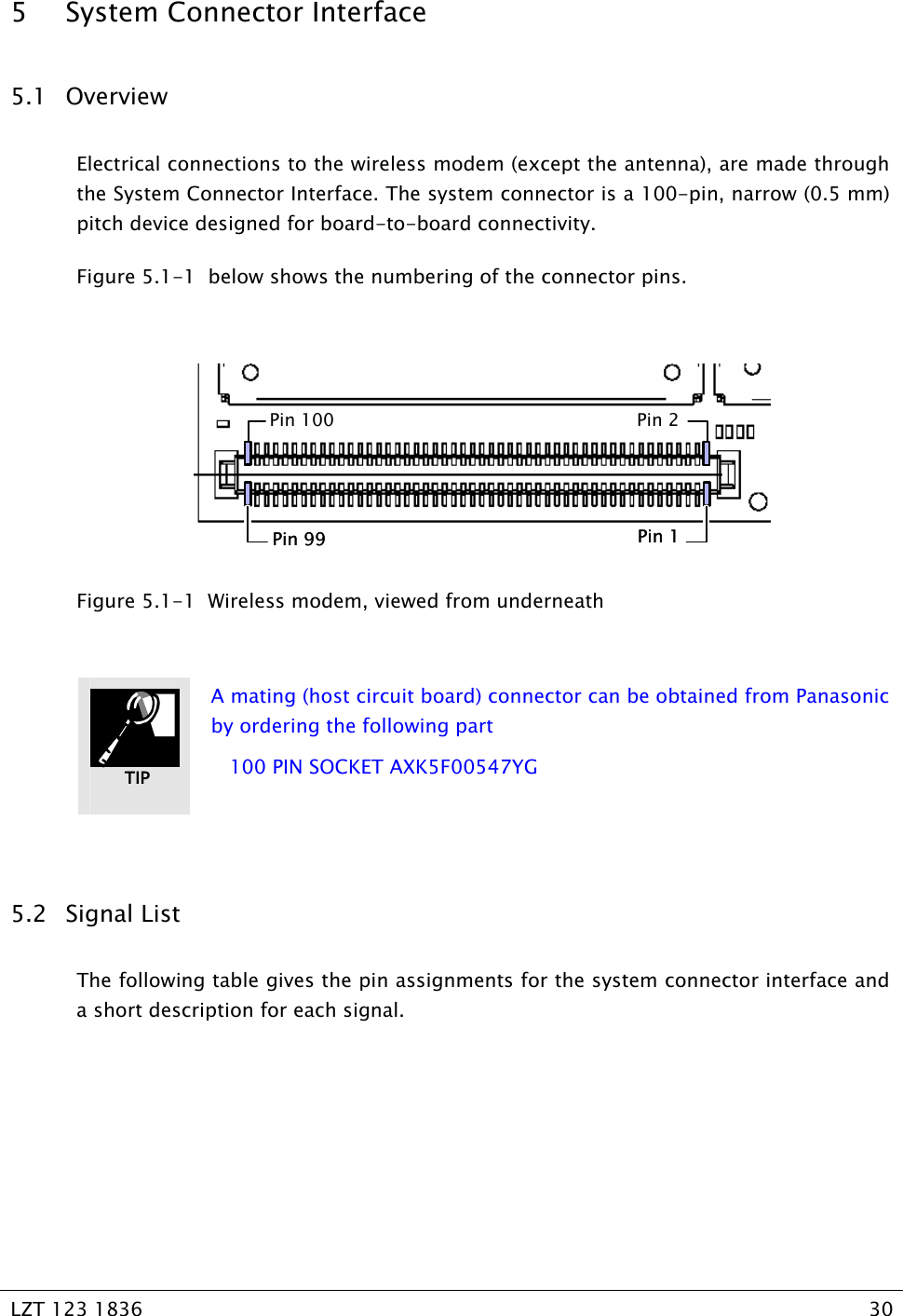
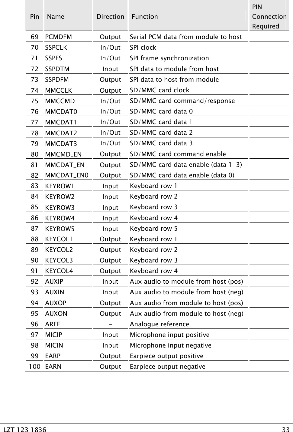
![LZT 123 1836 64 Signal Parameter Mode Min Typ Max Unit1.8V 0.9xSIMVCC V High level output voltage (VOH)3.0V 0.9xSIMVCC V 1.8V 0.4 V SIMCLK SIMRST Low level output voltage (VOL)3.0V 0.4 V 5.12.7 SIM Detection (SIMDET) SIMDET is used to determine whether a SIM card has been inserted into or removed from the SIM card holder. You should normally wire it to the ‘card inserted switch’ of the SIM card holder, but different implementations are possible. When left open, an internal pull-up resistor maintains the signal high and means ‘SIM card missing’ to the wireless modem. When pulled low the radio device assumes a SIM card is inserted. SIMDET is a Digital IO signal. In order to meet regulatory approval requirements, the SIMDET function must be implemented in the host application. 5.13 Synchronous Serial Port (SSP) Interface [to be implemented in a future release] Pin Name Direction Function 70 SSPCLK In/Out SPI clock 71 SSPFS In/Out SPI frame synchronization 72 SSPDTM Input SPI data to module from host 73 SSPDFM Output SPI data to host from module The SSP interface provides a synchronous serial peripheral interface based on the Motorola SPI protocol. The SSPI interface operates in a single master mode only, with the module acting as master. Four clock rates are supported through programming; 1.5MHz, 800kHz, 400kHz, 200kHz. The interface supports a variable word size, between 4bits to 16 bits. Continuous Transfer modes are not supported. The SSP supports programmable data sizes of 4 bits to 16 bits, in addition to which the polarity of the clock signal to the SPCLK pin is programmable through a register. NOTE](https://usermanual.wiki/Sony/BC051022/User-Guide-670126-Page-64.png)
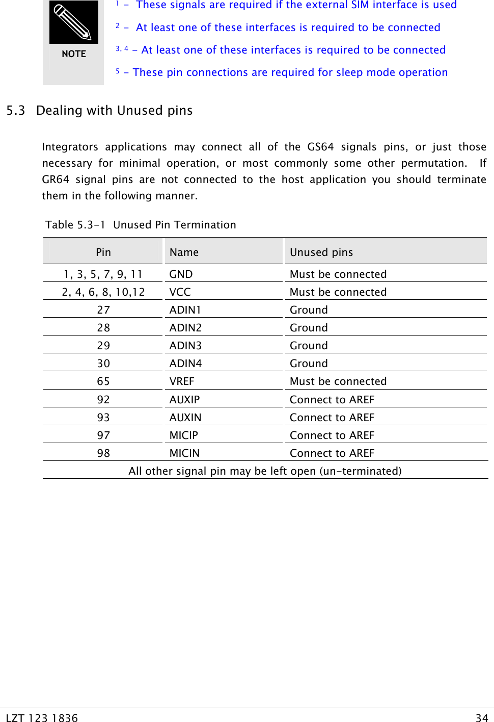
![LZT 123 1836 65 5.14 Memory Card Interface (SD/MMC) [to be implemented in a future release] Pin Name Direction Function 74 MMCCLK Output SD/MMC card clock 75 MMCCMD In/Out SD/MMC card command/response 76 MMCDAT0 In/Out SD/MMC card data 0 77 MMCDAT1 In/Out SD/MMC card data 1 78 MMCDAT2 In/Out SD/MMC card data 2 79 MMCDAT3 In/Out SD/MMC card data 3 80 MMCMD_EN Output SD/MMC card command enable 81 MMCDAT_EN Output SD/MMC card data enable (data 1-3) 82 MMCDAT_EN0 Output SD/MMC card data enable (data 0) SD/MMC interface module acts as either a multimedia card bus host or a secure digital memory card bus host. The interface conforms to the following standards: • Multimedia Card Specification v2.11 • Secure Digital Memory Card Physical Layer Specification v0.96 The SD/MMC interface provides around 800kbps net throughput. The SD/MMC interface, like all IO in the module, is 1.8V. In order to interface to some SD/MMC devices based on 3V technology it is necessary to level shift these signals for compatibility purposes. The MMC MD & DAT enable signals (pins 80, 81, 82) are provided to configure level shifters for directivity, which may be used with the Agere PSC2217 level shifter for example. There are other means of level shifting using bi-directional level shifters which do not require direction pins, such as: • Philips GTL2002, 2-bit bidirectional low voltage translators • Maxim MAX3001E, 8-channel bidirectional level translators 5.14.1 Multimedia Card System The multimedia card system transfers commands and data using three signal lines on a single physical bus:](https://usermanual.wiki/Sony/BC051022/User-Guide-670126-Page-65.png)
![LZT 123 1836 66 • MMCCLK: One bit is transferred on both command and data lines with each clock cycle. The clock frequency varies between 0 MHz and 20 MHz for a multimedia card. • MMCCMD: Bidirectional command channel that initializes a card and transfers commands. CMD has two operational modes; open-drain for initialization and push-pull for command transfer. This depends on speed requirements for the command channel during the initialization phase; external open-drain pull-up resistor may be needed if the 200 k internal pull-up resistor is too large. • MMCDAT: Bidirectional data channel, operating in push-pull mode. 5.14.2 Secure Digital Memory Card System The secure digital memory card system consists of the host and cards connected in a star topology. Multimedia cards and secure digital memory cards can be used in the same system. The power supply can be provided by the host or level-shifter devices such as Agere’s PSC2217. The following signals are used on the secure digital memory card bus: • MMCCLK: Host to card clock signal. • MMCCMD: Bidirectional command/response signal (one per card if multiple cards are connected to the bus, in which case, bus multiplexing logic is required). • MMCDAT[3:0]: Bidirectional data signals (one set per card). • VDD, VSS: Power and ground signals provided by the host or level translator product. The MCI (Multimedia Card Interface) does not contain bus multiplexing logic. If more than one secure digital memory cards needs to be supported, the user must implement bus multiplexing logic with external components.](https://usermanual.wiki/Sony/BC051022/User-Guide-670126-Page-66.png)
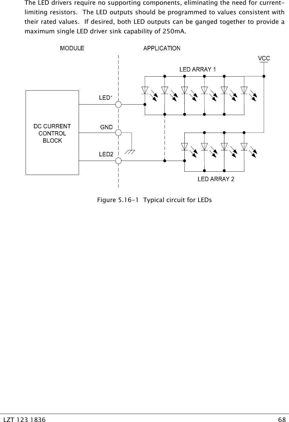
![LZT 123 1836 67 5.15 Service/Programming Pin Name Direction Function 20 SERVICE Input Flash programming enable signal The SERVICE interface is a standard IO, configured internally as an Input. This input is activated in order to enable flash memory programming. The SERVICE interface is normally pulled HIGH and is made active by the host application pulling it LOW. There are two methods for updating the firmware in the GR64: Sony Ericsson Emma III and Updater. The Emma III system is a web based tool that accesses a Sony Ericsson server from which signed software can be downloaded. The Updater is a local application that downloads a signed image provided by SEMC. 5.16 LED [to be implemented in a future release] Pin Name Direction Function 37 LED1 Output LED control signal 38 LED2 Output LED control signal The LED driver interface is able to operate single LEDs or a series of LEDs (such as LED backlighting). The LED interfaces are driven by programmable current sources, designed to control the brightness of the LEDs connected to them (typical of keyboard or LCD illumination). LED1 can be programmed to sink up to 75mA or 150mA in nonlinear steps over two ranges of output. LED2 can be programmed to sink from up to 50mA or 100mA in nonlinear step over two ranges of outputs. Both LED drivers are capable of sinking their maximum output current at a worst-case maximum output voltage of 0.4 V. For efficient use, the LEDs should be forward connected between the main battery and their corresponding LED driver output. NOTE](https://usermanual.wiki/Sony/BC051022/User-Guide-670126-Page-67.png)
![LZT 123 1836 78 5.22 Ringer Output (BUZZER) [to be implemented in a future release] Pin Name Direction Function 52 BUZZER Output Buzzer output Connecting the BUZZER signal to an inverting transistor-buffer followed by a piezoelectric transducer enables the wireless modem to play pre-programmed melodies or sounds.](https://usermanual.wiki/Sony/BC051022/User-Guide-670126-Page-78.png)