Star Micronics Tsp400 Users Manual Technical
TSP400 to the manual 258efb94-8230-4004-b82f-607bd7e7ab6d
2015-02-02
: Star-Micronics Star-Micronics-Tsp400-Users-Manual-487780 star-micronics-tsp400-users-manual-487780 star-micronics pdf
Open the PDF directly: View PDF ![]() .
.
Page Count: 80
- COVER
- NOTICE
- INTRODUCTION
- CHAPTER 1 SPECIFICATIONS AND OPERATION
- 1. General Specifications
- 2. External Appearance and Internal Configuration
- 3. DIP-Switch Settings
- 4. Print-Density Adjustment
- 5. Sensor Adjustment
- 6. Setting Memory Switches from the Control Panel
- 7. Test Print
- 8. HEX Dump
- 9. Page/Line Mode Switch
- 10. Exposing the Peripheral Unit Connector
- 11. Changing the Interface Board
- CHAPTER 2 THEORY OF OPERATION
- CHAPTER 3 PARTS REPLACEMENT AND RELATED ADJUSTMENTS
- CHAPTER 4 MAINTENANCE AND LUBRICATION
- CHAPTER 5 PARTS LIST
THERMAL PRINTER
TSP400 Series
TECHNICAL MANUAL
[THIRD EDITION]
NOTICE
•All rights reserved. Reproduction of any part of this manual in any form whatsoever,
without STAR’s express permission is forbidden.
•The contents of this manual are subject to change without notice.
•All efforts have been made to ensure the accuracy of the contents of this manual at the time
of going to press. However, should any errors be detected, STAR would greatly
appreciate being informed of them.
•The above notwithstanding, STAR can assume no responsibility for any errors in this
manual.
© Copyright 1994 Star Micronics Co., LTD.

INTRODUCTION
This manual is intended as a reference for maintenance personnel carrying out periodic maintenance or repair
in the field. It is not intended for general users.
• This manual is comprised of the following chapters.
Chapter 1 Specifications and Operation
Chapter 2 Theory of Operation
Chapter 3 Parts Replacement and Related Adjustments
Chapter 4 Maintenance and Lubrication
Chapter 5 Parts Lists
•First edition : Dec. 1994
Second edition : Jul. 1995
Third edition : March 1997
■Model Name
TSP 4 1 2 D — 120
Voltage
120 : 120VAC
220 : 220VAC
240 : 240VAC
Interface
D: RS232C
K: RS422A
C: Parallel
None: Without interface
Mechanism type
2: 40 columns
Printer type
1: Standard
4: With autocutter
TSP400-series thermal printer
1
2
3
4
5

CHAPTER 1
SPECIFICATIONS AND OPERATION
1. General Specifications ......................................................................................... 3
2. External Appearance and Internal Configuration .............................................. 4
3. DIP-Switch Settings .............................................................................................. 5
4. Print-Density Adjustment ..................................................................................... 8
5. Sensor Adjustment ............................................................................................... 9
6. Setting Memory Switches from the Control Panel........................................... 11
7. Test Print .............................................................................................................. 12
8. HEX Dump............................................................................................................ 12
9. Page/Line Mode Switch ...................................................................................... 13
10. Exposing the Peripheral Unit Connector .......................................................... 14
11. Changing the Interface Board ............................................................................ 15
1

– 2 –
SPECIFICATIONS AND OPERATION

– 3 –
SPECIFICATIONS AND OPERATION
1. General Specifications
Printing method Line thermal direct
Resolution 8 dots/mm (H) × 8 dots/mm (V)
Printable width 75 mm in Line Mode; 80 mm in Page Mode
Printing speeds 50 mm/sec and 25 mm/sec
Printable characters 1Page mode: ANK, International
2Line mode: ANK, International, Special, Block graphic, IBM
special, IBM block graphic, Kanji
NOTE: ANK is comprised of ASCII characters and katakana
Character matrixes 1Page mode
Small 8×16
Standard 16×24
Wide 24×32
OCR-B 16×24
2Line mode
Kanji 24×24 (12×24)
IBM block graphic 12×24 or 12×32
All others 12×24
Paper
Recommended brands TF50KS-E, TF62KS-E (Nippon Paper Industries)
KP50-HEAEX (New Oji Paper Co., Ltd.)
Width 82 mm (3.25 inches)
Thickness 60 to 150 µm
Roll diameters External 115 mm max.
Internal 25.4 mm (1 inch)
Interface RS232C, RS422A, or Parallel
Dimensions and weight Width 178 mm (TSP412D) 178 mm (TSP442D)
Depth 226 mm (TSP412D) 244 mm (TSP442D)
Height 256 mm (TSP412D) 256 mm (TSP442D)
Weight 3.4 kg (TSP412D) 3.7 kg (TSP442D)
Power supply 120VAC, 220VAC, 240VAC
Ambient conditions Operating 5˚C to 40˚C; 25%RH to 85%RH
Nonoperating -20˚C to 60˚C; 10%RH to 90%RH
Autocutter Lifetime 300,000 cuts (if paper debris is cleared)
Minimum cut length 25.4 mm (1 inch)
Fig. 1-1 External Dimensions
(TSP442)
(TSP412)
178mm
178mm
226mm
244mm
256mm
3.7kg
3.4kg
256mm
– 4 –
SPECIFICATIONS AND OPERATION
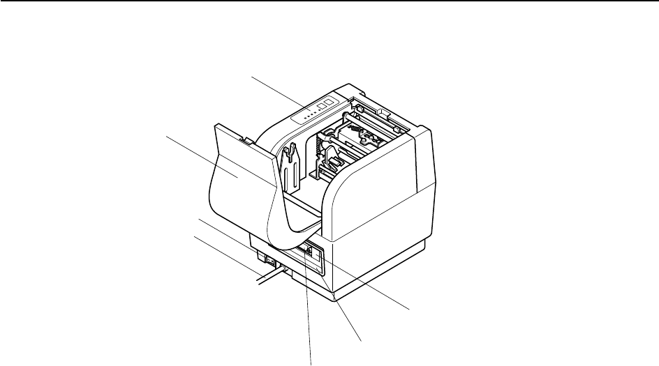
2. External Appearance and Internal Configuration
Fig. 1-2 Internal Configuration (TSP412D)
Control Panel
Interface connector
CONNECTOR COVER
(Peripheral unit connector)
Printer cover
Power cord
Power switch
Interface cover
– 5 –
SPECIFICATIONS AND OPERATION
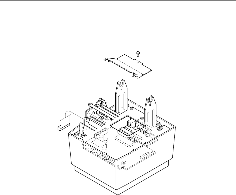
3. DIP-Switch Settings
DIP switches are located on the interface PCB. The number of switches depends on the interface type.
(1) Setting the DIP Switches
Fig. 1-3 DIP-Switch Settings
1Remove the screw holding the ROM cover in place. (The screw is located at the base of the paper-roll holder.)
2Remove the ROM cover, exposing the main and interface PCBs.
– 6 –
SPECIFICATIONS AND OPERATION
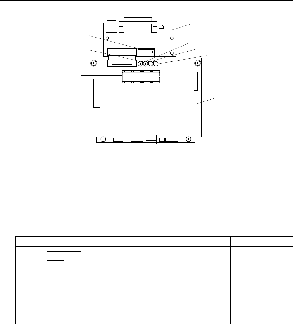
Fig. 1-4 Main and interface PCBs
3Set the DIP switches on the interface PCB.
2. DIP-switch values
1RS232C interface
This board has a single 8-bit DIP switch. Switch settings are as follows.
Switch Setting ON OFF
1-1 Baud
1-2
1-3 Handshaking DTR XON/XOFF
1-4 Data length 8 bits 7 bits
1-5 Parity use No parity Parity used
1-6 Parity type Odd Even
1-7 DC1/DC3 Ineffective Effective
1-8 Status of printer power
* All of these are set to ON before the printer is shipped from the factory.
Opening under ROM cover
EPROM
VP4 (Black-mark sensor) VR1 (Transmissive sensor -
coarse)
DIP switches
Interface PCB (RS232C)
VR3 (Paper-out sensor)
VR2 (Transmissive sensor - fine)
Main PCB
– 7 –
SPECIFICATIONS AND OPERATION
Baud 1-1 1-2
2400BPS OFF OFF
4800BPS OFF ON
9600BPS ON ON
19200BPS ON OFF
Mode Status of printer power
1-8 ON 1-8 OFF
DC1/DC3 invalid Printer selected Printer de-selected
DC1/DC3 effective Printer selected Printer de-selected
Addressable Printer de-selected Printer selected
To select a mode:
With an RS-232C interface, use DIP switches 1-7 to select the mode. With an RS-422A interface, use DIP switch
#2.
2RS422A interface
This board has two DIP-switches: one 8-bit switch and one 4-bit switch.
DIP switch #1 (8 bits):
Identical to the DIP switch on the RS232C (see above). But note that bit 1-7 is meaningless.
DIP switch #2 (4 bits):
SW2-1 SW2-2 SW3-3 SW2-4
DC1,3 off ON ON ON ON
Address #1 OFF ON ON ON
#2 ON OFF ON ON
#3 OFF OFF ON ON
#4 ON ON OFF ON
#5 OFF ON OFF ON
#6 ON OFF OFF ON
#7 OFF OFF OFF ON
#8 ON ON ON OFF
#9 OFF ON ON OFF
#10 ON OFF ON OFF
#11 OFF OFF ON OFF
#12 ON ON OFF OFF
#13 OFF ON OFF OFF
#14 ON OFF OFF OFF
DC1,3 mode on OFF OFF OFF OFF
* DIP-SW #2 overrides the DIP-SW #1 DC1/3 setting (bit 1-7).
* DIP-SW #2 factory setting: All ON
3Parallel (Centronics) interface
The parallel-interface board has no DIP switches.
– 8 –
SPECIFICATIONS AND OPERATION
Density Adjustment Aperture
About 90˚ About 90˚
Light Dark
4. Print-Density Adjustment
Adjust the print density in accordance with the sensitivity of the paper being used. The adjustment procedure is as follows.
Fig. 1-5 Print-Density Adjustment
1Remove the interface cover, located the rear side of the printer. The cover fits into place; no screws are used.
2The density adjustor (variable resistor) is now accessible through the aperture located to the left of the interface
connector.
3Insert a screwdriver (regular or phillips-head) into the aperture and rotate as necessary. The adjustor has a
rotational range of approximately 180 degrees.
4
5Avoid setting density too high for sensitive paper types. Excessive dark values may cause the paper to swell,
degrading the image quality.
6Some thermal papers may fail to produce a strong image when running at 50mm/sec printing speed, even at
maximum density setting. If you have this problem, reduce the print speed to 25mm/sec.

– 9 –
SPECIFICATIONS AND OPERATION
5. Sensor Adjustment
There are three different sensors: the transmissive sensor (label start-position detector), the black-mark sensor, and the
paper-out sensor. Adjustment procedures are described below. First note the following general points.
• The transmissive sensor level requires precise setting. Because transmission rates vary widely among different
types of label paper, we recommend that the sensor be readjusted each time the user changes to a different paper
type.
• Because black marks are likely to be similar across different paper types, the black-mark reflective sensor may
not require readjustment each time the paper type is changed. But you will still have to adjust it if the new paper
has a different consistency or uses a different black-mark density, or if the paper-feed routing is changed.
• In most generally not necessary to adjust the paper-out sensor.

– 10 –
SPECIFICATIONS AND OPERATION
Sensor adjustment procedures are as follows.
1) Remove the ROM cover, located beneath the paper-roll holding area.
2) Hold down the FEED and ON LINE buttons while switching on the power, and continue to hold them down until
you hear a triple beep. (This will take about five seconds.) When you hear the triple beep, release the buttons to
enter sensor-adjustment mode.
a) Reflective Sensor
• Insert a non-black area of paper into the mechanism’s sensor area.
• Rotate the main PCB’s reflective-sensor adjustment knob (VR4) to the point where the Head Up LED comes
on.
b) Paper-Out Sensor
• Insert a non-black area of paper into the mechanism’s sensor area.
• Rotate the main PCB’s paper-out-sensor adjustment knob (VR3) to the point where the Paper End LED switches
on.
c) Transmissive Sensor
• Insert the backing portion of a label sheet into the mechanism’s transmissive sensor area. (Insert the backing
part only, not the label itself.)
• Adjust the main PCB’s coarse (VR1) and fine (VR2) transmissive-sensor adjustment knobs to the point where
the Error LED comes on.
Note: When setting paper, be sure to lower the head so that it is close to its normal fixed position.
After the sensor has been adjusted, press the ON LINE switch to exit the sensor adjustment mode and return to the
normal operation mode.

– 11 –
SPECIFICATIONS AND OPERATION
6. Setting Memory Switches from the Control Panel
The TSP400 uses EEPROM memory switches in place of corresponding hardware switches. All EEPROM switch settings
can be changed by software. A number of these switches are also changeable from the control panel.
(1) Paper-Feed Mode (Continuous or Next-Top)
When the feed mode is set to next-top, the printer can come online only if loaded with labels or marked paper. If the printer
fails to come online you will not be able to change the feed-mode setting by command; you will therefore have to change
it using the control panel.
1Hold down the FEED and ON LINE buttons while switching on the power, and continue to hold them down until
you hear a double beep. (You will first hear a single beep, followed by a pause, followed by the double beep.)
Release the buttons immediately after hearing the double beep.
2Press the ON LINE button to select continuous feed (the printer beeps once), or press the FEED button to select
next-top feed (the printer beeps twice). If you select next-top feed, the printer automatically starts paper feed
and looks for the next top.
(2) Sensor Mode
The printer may be set to use either the transmissive or the reflective sensor for next-top detection. You can make this
setting as follows.
1Hold down the ON LINE button while switching on the power, then continue to hold it down until you hear a
double beep. (You will first hear a single beep, then a pause, then the double beep.) Release the ON LINE button
immediately after hearing the double beep.
2Press the ON LINE button to select the reflective sensor (the buzzer beeps once), or press the FEED button to
select the transmissive sensor (the buzzer beeps twice).

– 12 –
SPECIFICATIONS AND OPERATION
7. Test Print
To generate a test print (self-test), hold down the FEED button while switching on the power.
Note: The test print continues as long as the FEED button is held down.
8. HEX Dump
Set the printer into hex-dump mode as follows: hold down the ONLINE button and switch the power on, then release the
ONLINE button as soon as you hear a single beep. The printer is now set to print a hex dump of the data sent from the
host.
Note: The HEX Dump mode continues to be effective until the power supply is turned off.

– 13 –
SPECIFICATIONS AND OPERATION
9. Page/Line Mode Switch
The TSP400 series supports two entirely different command sets: “Page Mode” and “Line Mode.” You can select the
mode either by software or from the control panel. To select from the control panel, proceed as follows.
NOTE: This function will not become meaningful until Line Mode
software has been introduced.
1Hold down the ON LINE button while switching on the power, then continue to hold it down until you hear a
triple beep. (This will take about five seconds.)
2Press the ON LINE button to select Page Mode (the buzzer beeps once), or press the FEED button to select Line
Mode (the buzzer beeps twice).
– 14 –
SPECIFICATIONS AND OPERATION
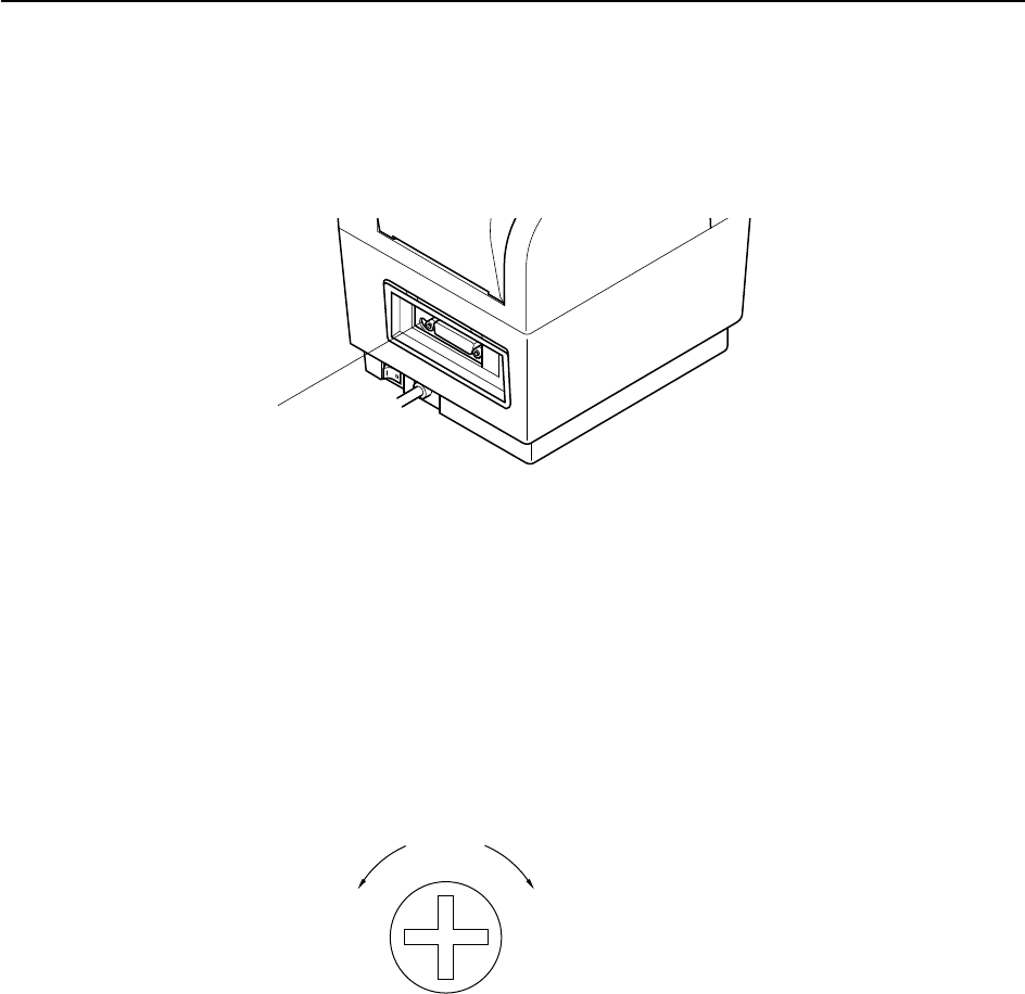
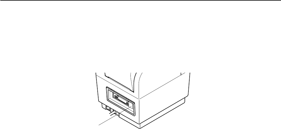
10. Exposing the Peripheral Unit Connector
When operating in Line Mode, the printer can use the peripheral unit connector to drive a cash drawer or other such external
device. But note that the connector is originally hidden by a portion of the interface cover.
Fig. 1-6 Peripheral Unit Connector
To prepare the connector for use, remove the “connector cover” portion of the interface cover (see illustration) by gently
bending and breaking it with a pliers. Be sure to remove any remaining burrs using a cutter or other such tool.
Connector cover
– 15 –
SPECIFICATIONS AND OPERATION
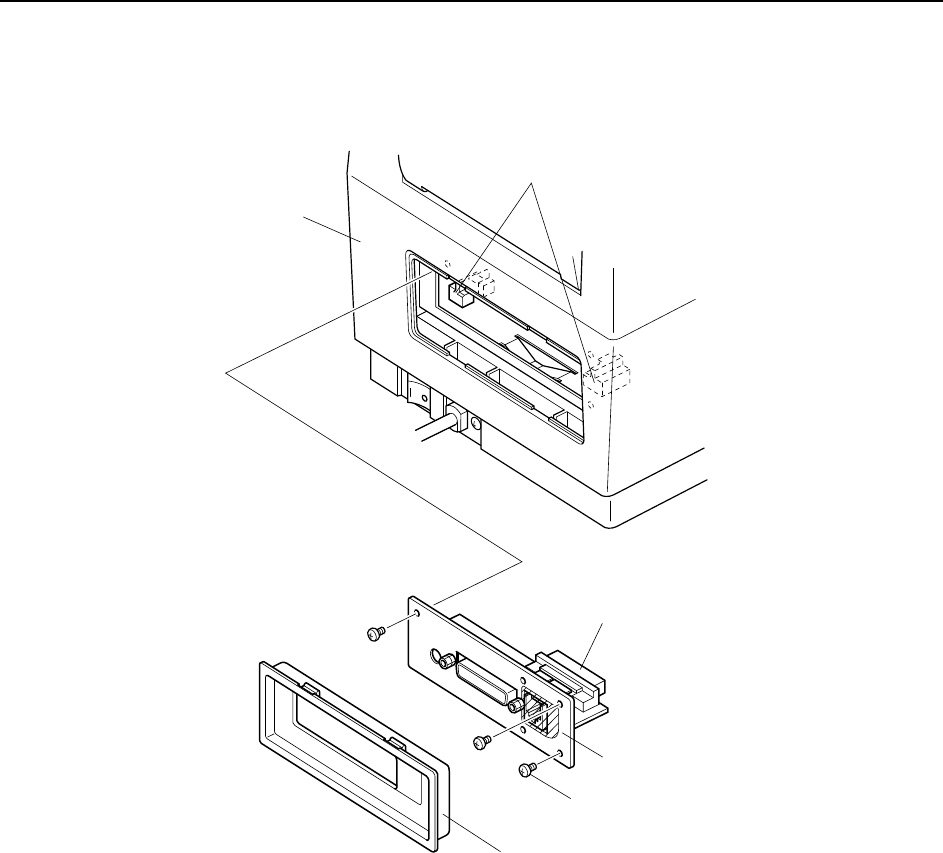
11. Changing the Interface Board
You can change the printer’s interface by replacing the interface board. The replacement procedure is as follows.
Fig. 1-7 Changing the Interface Board
1Remove the interface cover, located on the rear side of the printer.
2Remove the three screws holding the interface board in place.
3Remove out the board by pulling on the pull sheet fastened to the connector.
4Fit the replacement interface board to the guides and push all the way in so that the connector is fully engaged.
5Fasten the outer plate to the printer with three screws.
6Replace the interface cover.
Note: The printer automatically detects changes in interface type.
Interface
board
Screws (3)
Interface cover
Interface board PCB guide
Printer
Connector

– 16 –
SPECIFICATIONS AND OPERATION

CHAPTER 2
THEORY OF OPERATION
This chapter describes the operating principles of the circuitry and printer mechanism.
1. Block Diagram ..................................................................................................... 19
2. Main and Interface PCBs .................................................................................... 21
2-1. Interface ................................................................................................................. 21
2-1-1. RS232C .............................................................................................................. 21
2-1-2. RS422A .............................................................................................................. 22
2-1-3. Parallel interface ............................................................................................... 23
2-2. Editing and Printing .............................................................................................. 24
2-2-1. Editing ............................................................................................................... 24
2-2-2. Thermal head .................................................................................................... 24
2-2-3. Head current control ........................................................................................ 25
2-3. Feed-Motor Drive Circuit ...................................................................................... 26
2-4. Power-On Reset Circuit ........................................................................................ 27
2-5. +5V Line Voltage Detector Circuit ....................................................................... 28
3. Printer Mechanism .............................................................................................. 29
3-1. Thermal Head ........................................................................................................ 29
3-2. Paper-Feed Mechanism ........................................................................................ 29
3-3. Detectors ............................................................................................................... 30
2

– 18 –
THEORY OF OPERATION
– 19 –
THEORY OF OPERATION
1. Block Diagram
The following diagram illustrates the relationship between the control board (main PCB) and its peripherals.
(16)
(16)
(8)
(8)
(16)
24V
Data flow (Host computer)
Control
panel
Main PCB
Gate array
CPU
DC-DC converter
Power unit
EPROM
128K × 16bits
PS-RAM
128K × 16bits
S-RAM (backup)
8K × 8 bits
Kanji ROM
256K × 16 bits
EEPROM
Head driver
Motor driver
Cutter driver
Sensor circuitry
External device
driver
Thermal
head
Printer mechanism
Feed motor
Autocutter
Sensor
External
device
Interface board
RS232C, RS422A, or parallel
Fig. 2-1 Block Diagram

– 20 –
THEORY OF OPERATION
1. 1 Control board
The interface board relays data from the host computer to the main board. The main board’s CPU stores the data
into local RAM.
It then reads out the data, edits it according to the control program stored in the board’s ROM, and prints the results
by issuing appropriate drive signals to the printer mechanism.
[Block Description]
a. CPU: HD641300F10T
CMOS single-chip computer
Controls overall printer operation.
b. EPROM: 128 K × 16 bits
Contains the CPU control program.
c. PS-RAM: 128 K × 16 bits
Work area and data buffer
d. S-RAM
Saves format data and externally defined characters.
Backed up by super capacitor.
e. EEPROM: 1024 bits
Stores printer settings. Settings can be changed by software. (Used in place of dip-switches.)
f. Interface board
Interfaces the main board with the host computer.
There are three versions, each for a different interface type: RS232C, RS422A, or Centronics parallel.
g. Gate array
Executes various types of signal processing.
h. Drivers
The various drivers convert signals received from the CPU and gate array into the drive signals that directly
control the printer mechanism.
i. DC-DC converter
Converts the supplied 24V to 5V.
1. 2 Control Panel
Provides manual control switches and operational indicators.
1. 3 Printer mechanism
Comprised of thermal head, paper-feed motor, and sensor mechanism.
1. 4 Power unit
Converts primary power to DC24V.
1. 5 External device
External device (such as cash drawer) driven by signals issued by the control board.
– 21 –
THEORY OF OPERATION
D2O
D1O
R1I
R2I
D2I
D1I
R1O
R2O
B12
B14
A15
B15
ACKDTR
R-CH
TXD
RXD
CTS
TXD0
RXD0
RXD1
CN3 CN1
IC1
CN9 IC10
IC5
Gate array
CPU
HD151232FP
B12
B14
A15
B15
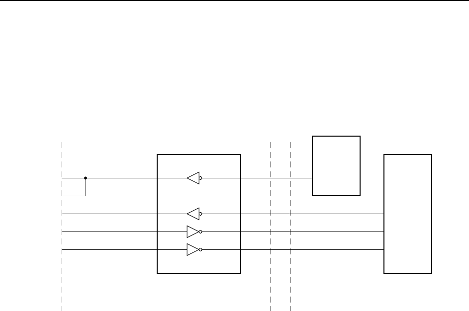
2. Main and Interface PCBs
The main PCB and interface PCB provide the drive circuitry for the TSP-400 printer series. The two boards are connected
via 40-pin connectors.
2-1. Interface
2-1-1. RS232C interface
RS232C Interface PCB Main PCB
Fig. 2-2 RS232C Interface
Data flow from host to printer: IC1 receives serial data from the host computer via RXD, converts the signal voltage
from RS232C level to TTL level, and passes the result to the CPU. The CPU converts the serial data to parallel and stores
it into buffer memory.
Data flow from printer to host: The CPU generates data, converts it into serial form, then passes it to IC1. IC1 converts
the signal voltage from TTL level to RS232C level, then outputs the result over the TXD line.
The CTS line is hardware-connected, but the connection is not recognized by software. (The printer does not monitor the
signal.)
– 22 –
THEORY OF OPERATION
D2O
D1O
D2EN
D2I
D1EN
D1I
ERROR
ACK
RD (+)
RD (–)
CS (+)
CS (–)
RS (–)
RS (+)
SD (–)
SD (+)
CN3 CN1
IC1
+
–
+
–
Gate array
CN9 IC10
R2I
+
R2I
–
R1I
+
R1I
–
D2O
D2O
D1O
D1O
RXD0
TXD0
RXD1
CPU
IC5
A15
B15
A10
B12
B14
A15
B15
A10
B12
B14
MC34051
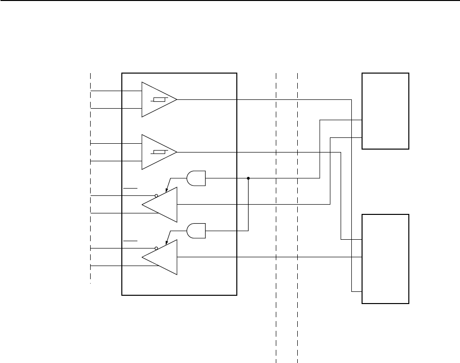
2-1-2. RS422A interface
RS422A Interface PCB Main PCB
Fig. 2-3 RS422A Interface
IC1 operates as the RS422A driver and receiver.
Data flow from host to printer: IC1 receives serial data from the host computer via RD, converts the signal voltage from
RS422A level to TTL level, and passes the result to the CPU. The CPU converts the serial data to parallel and stores it
into buffer memory.
Data flow from printer to host: The CPU generates data, converts it into serial form, then passes it to IC1. IC1 converts
the signal voltage from TTL level to RS422A level, then outputs the result over the SD line.
The CS line is hardware-connected, but the connection is not recognized by software. (The printer does not monitor the
signal.)
– 23 –
THEORY OF OPERATION
Parallel Interface PCB Main PCB
DATA 1
DATA 2
DARA 3
DATA 4
DATA 5
DARA 6
DATA 7
DATA 8
STROBE
BUSY
ACK
ERROR
SELECTED
PAPER OUT
A4
B4
A5
B5
A6
B6
A7
B7
A13
A12
B12
A10
A11
B11
CN3
CPU
CN1
IC5
CN9
A4
B4
A5
B5
A6
B6
A7
B7
A13
A12
B12
A10
A11
B11
Gate array
IC10
LS05
IC1
CD0
CD1
CD2
CD3
CD4
CD5
CD6
CD7
CSTB
BUSY
ACK
ERROR
SELECT
POUT
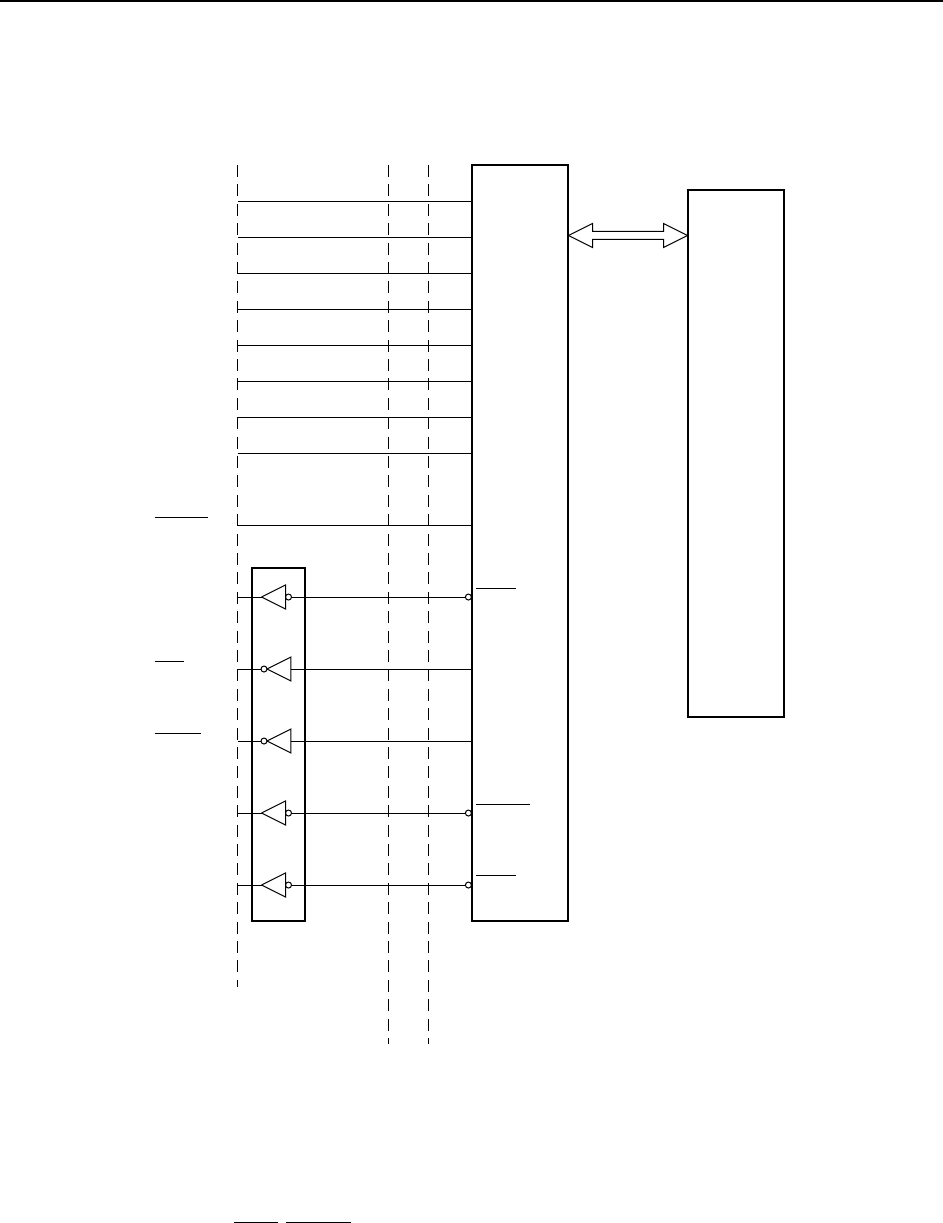
2-1-3. Parallel interface
Fig. 2-4 Parallel Interface
The host computer sends eight bits of parallel data to CN3 when the printer is ready (when BUSY is LOW).
The data passes through the interface PCB and gate array, then moves into the CPU.
Printer signals from the CPU (ACK, ERROR, SELECTED, PAPER OUT, etc.) pass through the gate array and are output
over the appropriate connector pins.
– 24 –
THEORY OF OPERATION
2-2. Editing and Printing
2-2-1. Editing
The CPU reads data sequentially from RAM and edits it in accordance with program instructions stored in EPROM. The
edited data undergoes parallel-to-serial conversion in the gate array, and is then output to the thermal head’s drive
controller.
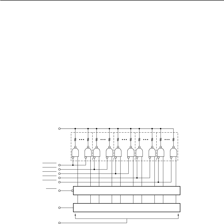
2-2-2. Thermal head
The thermal head contains 640 heat elements. Printing is carried out by switching these elements ON or OFF as required.
Note that Line Mode supports 600-dot printing only. During Line Mode operation, therefore, the logic always sends OFF
data to elements 1 to 20 and 621 to 640.
The thermal head contains a dedicated drive controller. The controller consists of a shift register, a latch circuit, and a
driver circuit, as illustrated below. The drive controller receives serial data (SI) from the drive control board in sync with
the CLOCK signal. The controller latches the incoming data (LATCH), then outputs it to the heat elements in sync with
the trailing edge of the STROBE signals. A data value of LOW corresponds to a heat-element value of ON.
Fig. 2-5 Thermal-Head Drive Circuit
STROBE5
STROBE4
STROBE3
STROBE2
STROBE1
LATCH
SI
CLOCK
COM
Latch
Shift Register
– 25 –
THEORY OF OPERATION
24V
t
CLOCK
SI
LATCH
STROBE1
STROBE2
STROBE3
STROBE4
STROBE5
COMMON
STROBE1, STROBE2, STROBE3
STROBE4, STROBE5,
t t
10 20 30 40 50
300
400
500
Head Energizing Time
t (µsec)
Thermistor Temp. (°C)
600
Fig.2-6 Timing Chart
2-2-3. Head current control
Heat buildup in the head during operation can cause print quality to degrade. To maintain uniform quality, the printer
varies the energizing time (time that STROBE remains LOW) in accordance with the head temperature.
The thermal head’s surface temperature is calculated based on the resistance value of an attached thermistor. Energizing
time is reduced at higher temperatures, as indicated in the figure 2-6.
Fig. 2-7 Head Energizing Control
– 26 –
THEORY OF OPERATION
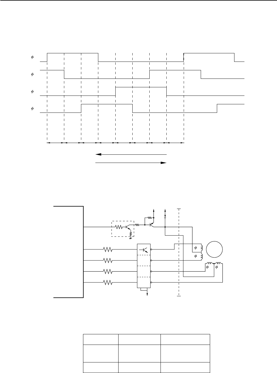
2-3. Feed-Motor Drive Circuit
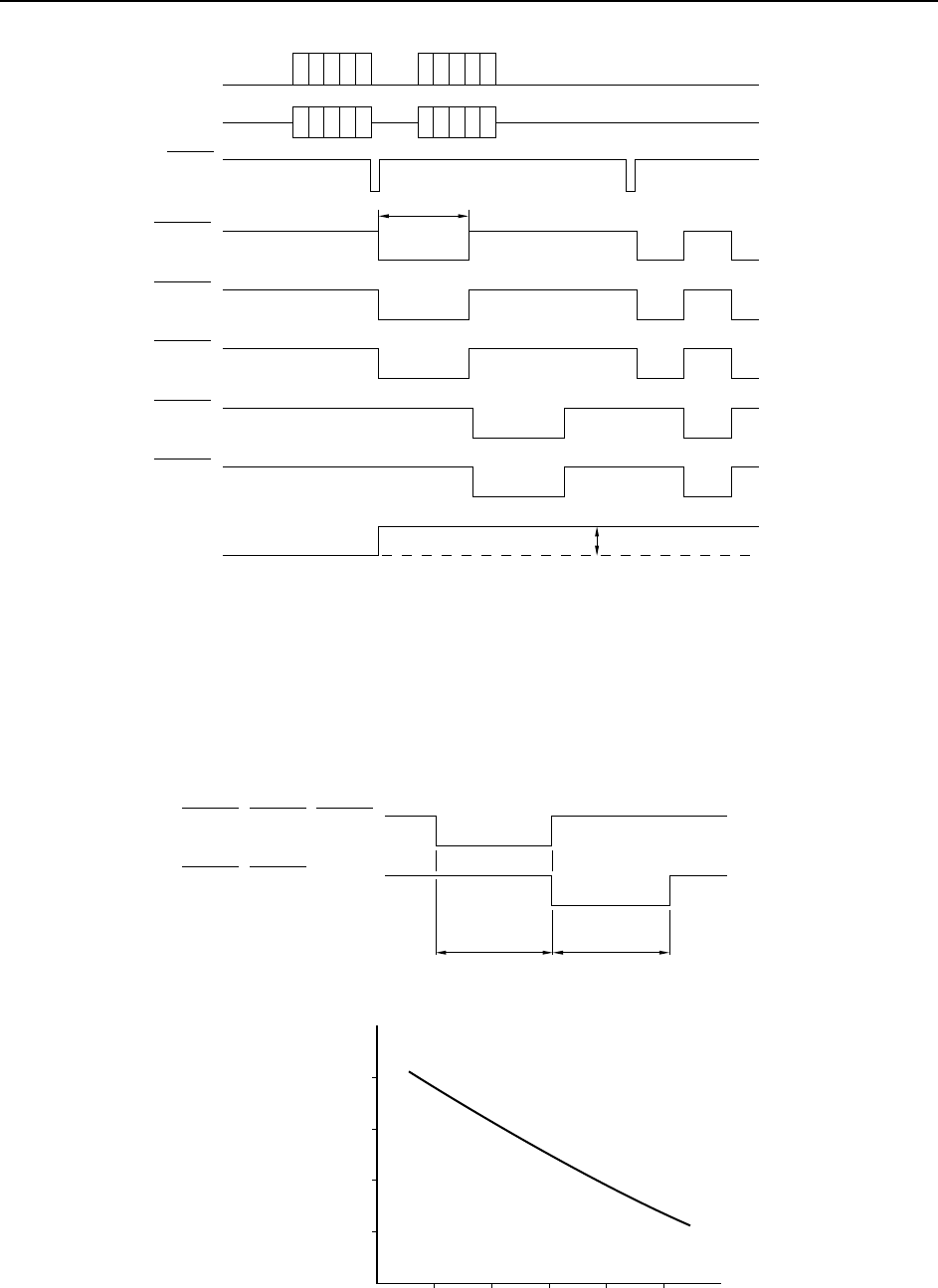
The printer employs a 4-phase step motor (phase 1-2 excitation) to implement paper feed. The motor rotates through a
certain angle each time it receives a pulse from the drive circuit. The following diagram illustrates the phase 1-2 excitation
method. Diagram 2-8 shows the feed-motor drive circuit.
Fig. 2-8 Motor Control by Phase 1-2 Excitation
Fig. 2-9 Feed-Motor Drive Circuit
Voltage to the motor is controlled to produced the required action, as follows.
Mode Voltage Action
Operating VM (+24V) Drives the motor
VL (+5V)
Idle VL (+5V) Holds the motor
Voltage is controlled by PA4 of the CPU, which goes HIGH or LOW to switch transistors DQ2 and Q2 ON or OFF. When
Q2 is ON, the motor receives +24V (VM). When Q2 is OFF, +5V is supplied to the motor via diode D1.
1 2 3 4 5 6 7 8
1
2
3
4
ON
ON
ON
ON
ON
Step
PA4
PA0
PA2
PA3
PA1
1
2
3
4
CN4
1
2
4
5
6
3
M
+5V+24V
Q2
D1
TA1
B
DQ2
M-GND
E
IC5
CPU
Paper-feed motor
Forward Feed
Reverse Feed
– 27 –
THEORY OF OPERATION
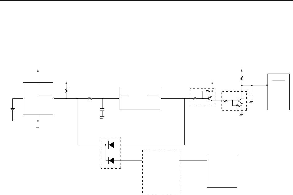
2-4. Power-On Reset Circuit
Immediately following power-on the printer executes a power-on reset, initializing all circuit elements. The power-on
reset serves as protection against operational errors. The power-on RESET signal is maintained for approximately 160ms.
The reset circuit is illustrated below.
Fig. 2-10 Power-On Reset Circuit
1At power on, voltage-detector circuit IC4 (M51953BL) outputs a LOW signal from its OUT terminal. The signal
lasts for approximately 160ms, as determined by capacitor C2 (0.47µF):
T = 0.34 × C2 (pF) [µs] = 160ms
2The LOW signal resets the CPU and the mechanism drive circuits, and sets S-RAM into backup state.
+5V
IC4
CD
C2 GND
+5V
+5V
+5V
VCC
RESET
DD3
IC5 : CPU
RES RESO
RESET
VCC
S-RAM
+
Gate
array
IC1
RESET IC
IC10
Back-up
Circuit
CPU
– 28 –
THEORY OF OPERATION
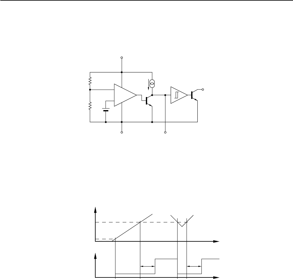
2-5. +5V Line Voltage Detector Circuit
The voltage-detection IC (IC4 in Fig. 2-10) detects momentary drops or unstable levels in the +5V line voltage. IC4
operation is illustrated by the equivalence circuit shown below.
Fig. 2-11 Equivalence Circuit for Voltage Detecting IC
Fig. 2-11 shows the operational timing. If the +5V line voltage falls below 4.25V, the IC produces a reset signal at its
OUTPUT terminal, resetting the CPU and the gate array.
Fig. 2-12 Operation Timing Chart
1.25V
R1
R2
SµA typ
VCC
1
GND
3Cd4
–
OUT
5
–
+
VCC Voltage
4.25V
0.8V
Output
Voltage
tdtd
t
t
td = 0.34 × Cd (pF) [µs]
– 29 –
THEORY OF OPERATION
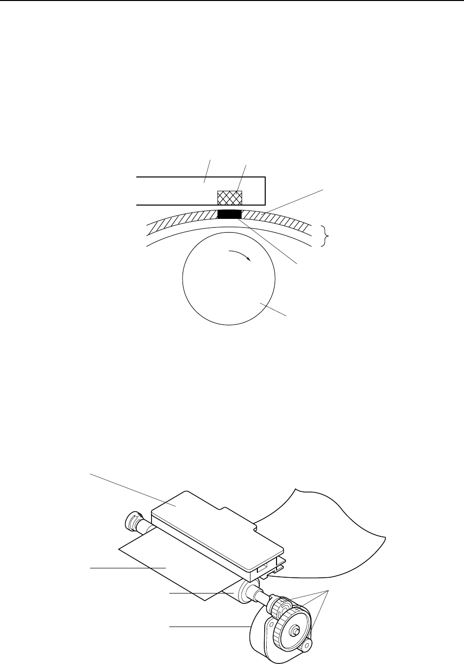
3. Printer Mechanism
3-1. Thermal Head
The TSP400 printers employ thermal line printing. The thermal head consists of a horizontal line of 640 heat elements.
These elements print one line of dots at a time as the paper passes over the head. The head is fixed in position; only the
paper moves.
The printer prints a dot by heating the corresponding heat element. The heated element causes a chemical reaction in the
coloring layer of the thermal paper, resulting in the formation of a visible dot.
Fig. 2-13 Principle of Thermal Printing
3-2. Paper-Feed Mechanism
The paper-feed mechanism is comprised of the paper-feed motor, gear train, platen, and thermal head. The paper-feed
motor drives the gear train, which in turn rotates the platen. The platen carries the thermal paper past the thermal head.
The paper-feed motor is a PM (permanent magnet) type, 4-phase 48-pole step motor. A single step feeds the paper
approximately 0.125mm.
Fig. 2-14 Paper-Feed Mechanism
Thermal head Heat element
Coloring layer
Platen
Printed point
Thermal paper
Thermal paper
Platen
Paper-feed motor
Thermal head
Gear train
– 30 –
THEORY OF OPERATION
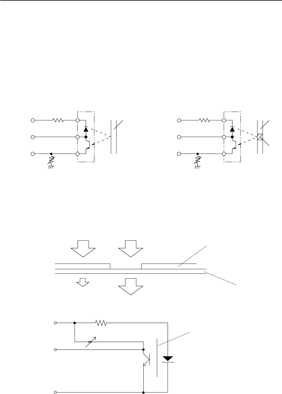
3-3. Detectors
(1) Paper-Out Detector
The paper-out detector is located at the paper entry slit. The detector consists of a reflective photosensor. The
photosensor’s phototransistor remains ON while paper is present. It goes OFF when paper runs out, generating
output of a paper-out signal.
(2) Black-Mark Detector
This detector senses black marks indicating print start positions. The detector is useful only with specially marked
paper. Like the paper-out detector, the black-mark detector consists of a reflective photosensor. The photosensor’s
phototransistor goes OFF when a black mark appears.
Fig. 2-15 Paper-Out Detector Fig. 2-16 Black-Mark Detector
(3) Label Detector
The transmissive detector is used to detect print-start positions for labels. It operates by detecting the difference
in light transmission between backing-only and backing-plus-label portions of the paper.
Fig. 2-17
Fig. 2-18 Label Detector
GND
+5V
R
R
GND
+5V
R
R
Paper
(Reflective photosensor)
Detection signal Detection signal
Paper
Black mark
(Reflective photosensor)
Light Light
Backing paper
Quantity of
transmitted light Quantity of
transmitted light
5V
Paper
Label paper
Detection signal
GND

– 31 –
THEORY OF OPERATION
(4) Head-Up Detector
This detector consists of a leaf switch indicating whether the head is closed (in contact with the platen) or open
(separated from the platen). The leaf switch is closed when the head is closed; it opens when the head is opened.
Fig. 2-19 Head-Up Detector
GND
R
+5V
Leaf switch
Detection signal

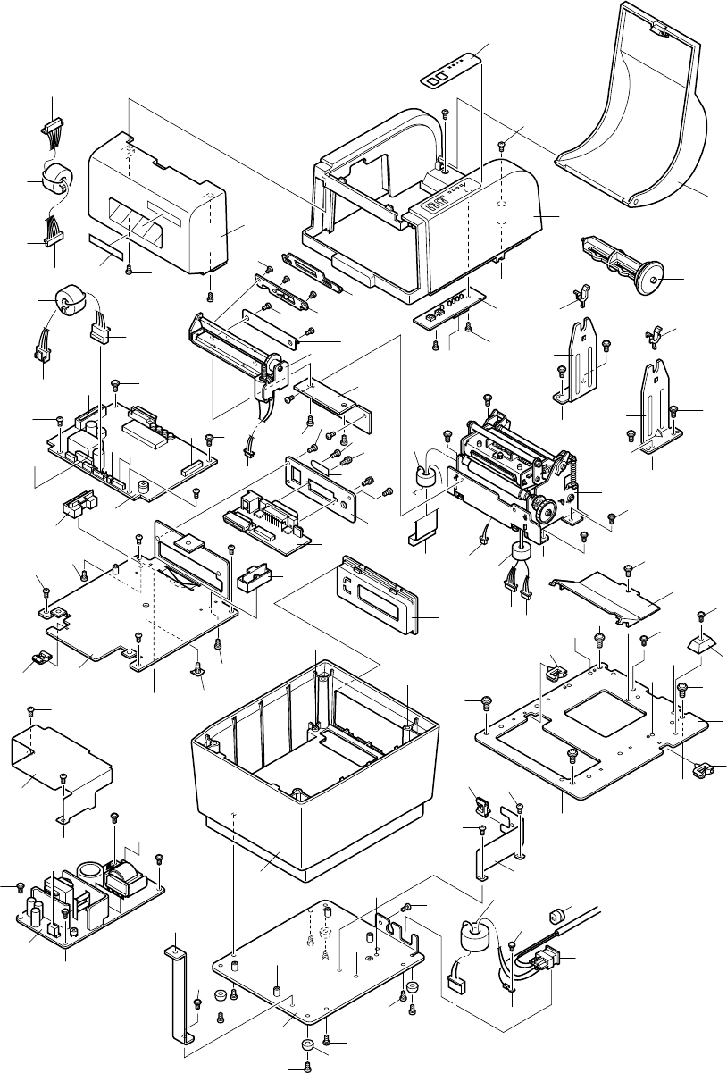
CHAPTER 3
PARTS REPLACEMENT AND RELATED ADJUSTMENTS
This chapter describes disassembly and reassembly procedures.
Please take note of the following.
1. ALWAYS disconnect the power cord from the AC outlet before beginning a disassembly or reassembly
procedure.
2. Except where otherwise stated, the reassembly procedure is the reverse of the disassembly procedure.
3. Coat screw heads with locking sealant after completion of reassembly.
4. Refer to Chapter 4 Section 2 for important information about lubrication requirements.
Note:The printer has no adjustable parts.
1. Upper Casing Unit ............................................................................................... 35
2. Control-Panel Board ........................................................................................... 36
3. Printer Mechanism .............................................................................................. 37
4. Main PCB, Interface PCB .................................................................................... 38
5. Power Unit ........................................................................................................... 39
6. Fuse ...................................................................................................................... 39
7. Printhead Unit...................................................................................................... 40
8. Feed Motor Assembly ......................................................................................... 40
9. Detectors .............................................................................................................. 41
10. Label sensor..................................................................................................................... 41
3

PARTS REPLACEMENT
– 34 –
PARTS REPLACEMENT
– 35 –
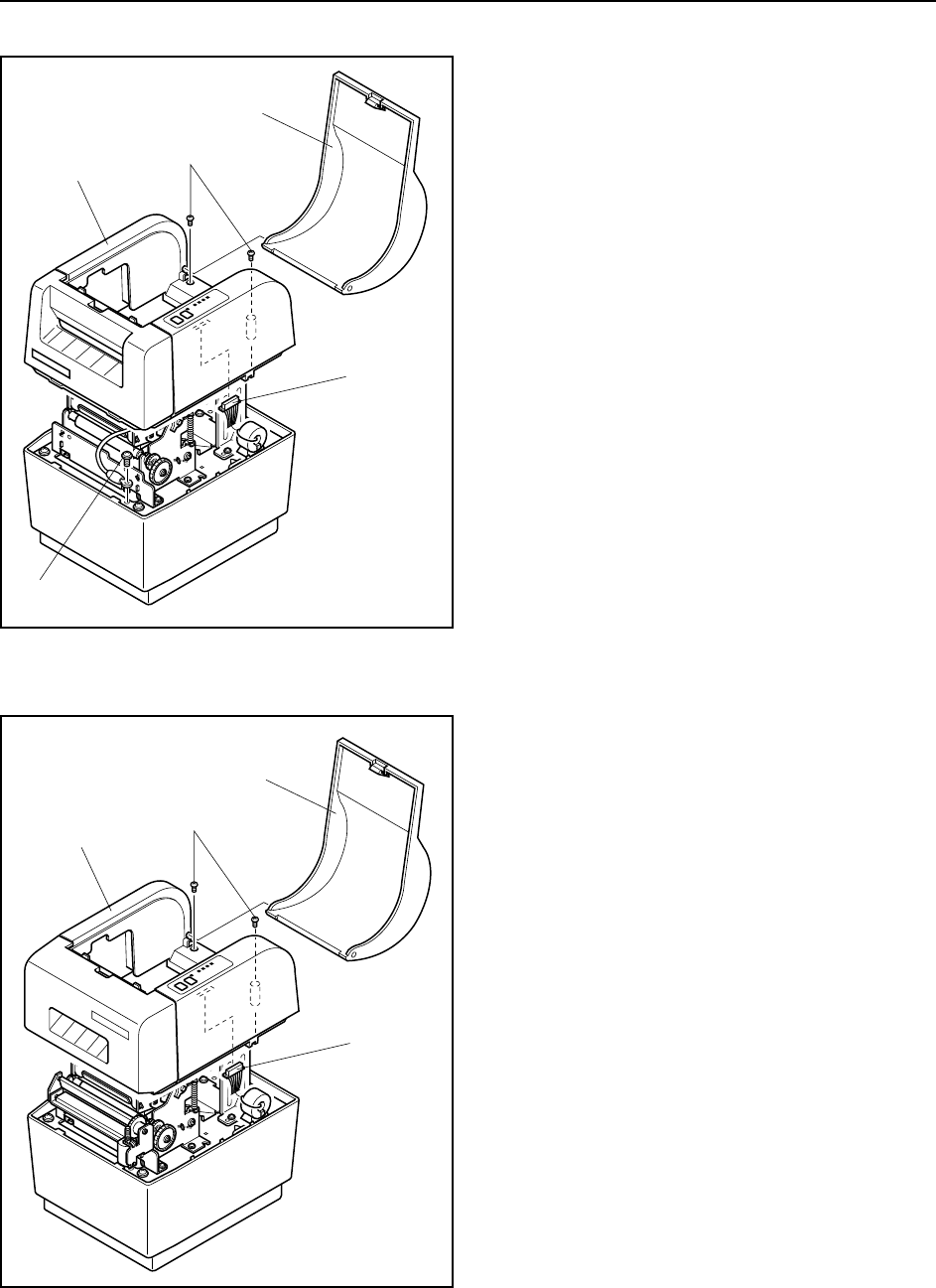
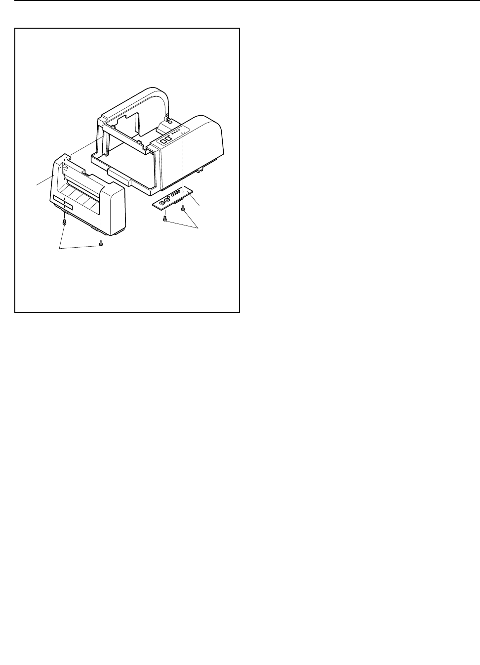
1. Upper Casing Unit
<TSP412D>
(1) Disconnect the power cord from the AC outlet.
(2) Remove:
•Upper cover 1
•Two tapping screws 2
•Upper casing unit 3
•Pull forward and remove.
•Connector 4
•Screw 5
<TSP442D>
(1) Disconnect the power cord from the AC outlet.
(2) Remove:
•Upper cover 1
•Two tapping screws 2
•Upper casing unit 3
Pull forward and remove.
•Connector 4
3
1
2
4
5
3
1
2
4
PARTS REPLACEMENT
– 36 –
2. Control-Panel Board
(1) Remove:
•Upper casing unit (See 1. above.)
•Two tapping screws 1
•Front cover 2
•Two tapping screws 3
•Control-panel board 4
1
3
4
2
PARTS REPLACEMENT
– 37 –
3
21
3
4
6
4
3
5
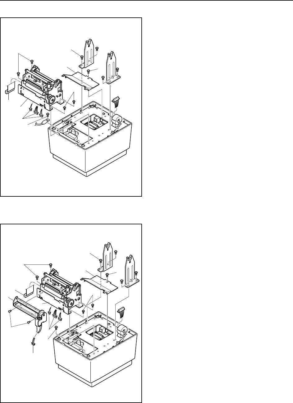
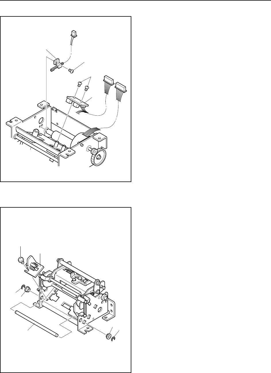
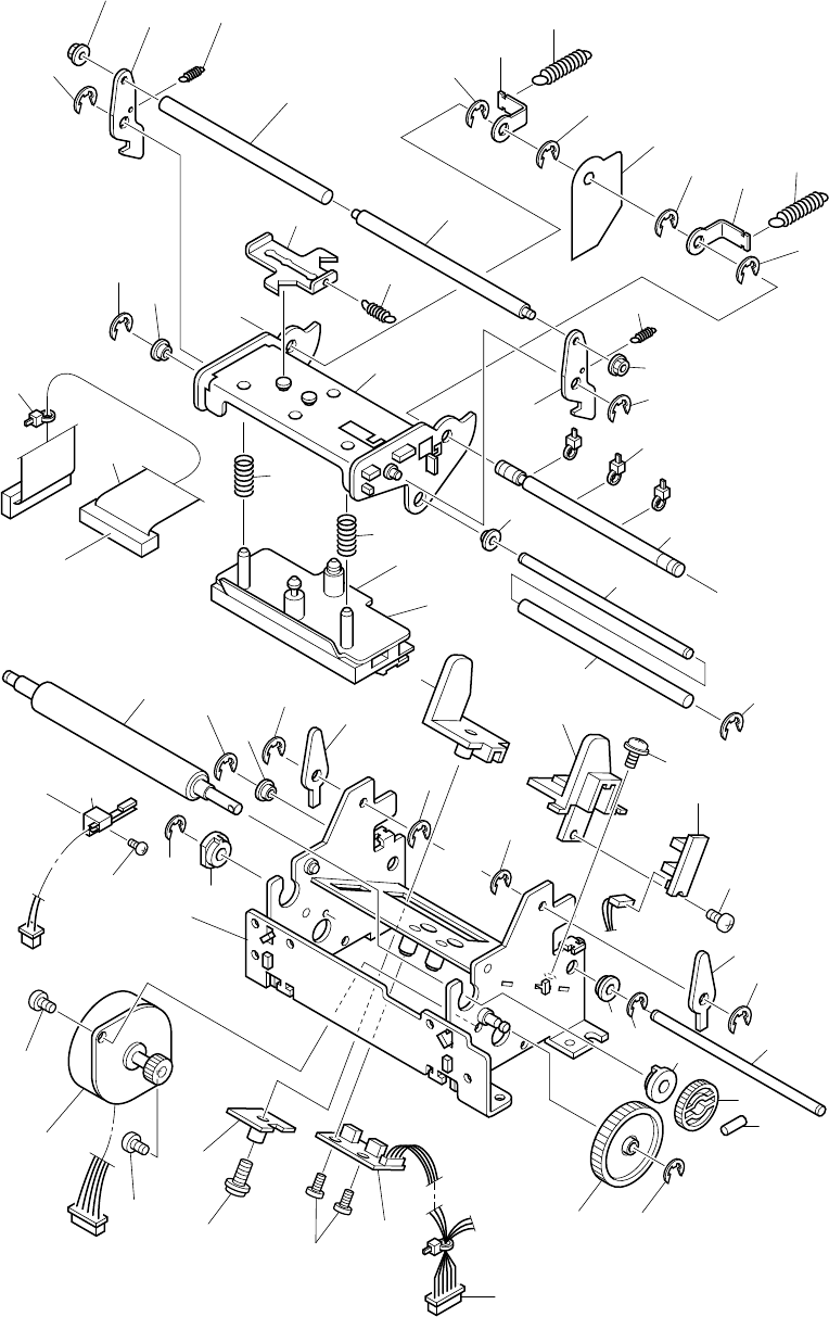
3. Printer Mechanism
<TSP412D>
(1) Remove:
•Upper casing unit (See 1. above.)
•One tapping screw 1
•ROM cover 2
•Eight tapping screws 3
•Four connectors 4
•Screw 5
•Printer mechanism 6
<TSP442D>
(1) Remove:
•Upper casing unit (See 1. above.)
•One tapping screw 1
•ROM cover 2
•Eight tapping screws 3
•Five connectors 4
•Two tapping screws 5
•Cutter unit 6
•Screw 7
•Printer mechanism 8
7
3
21
3
5
4
3
4
6
4
8
PARTS REPLACEMENT
– 38 –
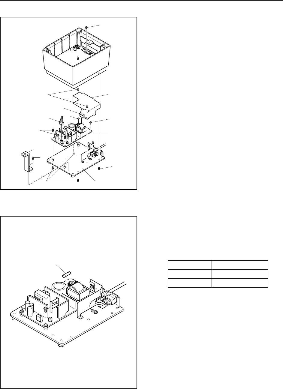
4. Main PCB, Interface PCB
<TSP412D>
(1) Remove:
•Upper casing unit (See 1. above.)
•Six tapping screws 1
•Mechanism chassis 2
•Six connectors 3
•Interface cover 8
•Three screws 4
•Interface PCB 5
•Four screws 6
•Main PCB 7
<TSP442D>
(1) Remove:
•Upper casing unit (See 1. above.)
•1 screw
•Four tapping screws 1
•Mechanism chassis 2
•Seven connectors 3
•Interface cover 8
•Three screws 4
•Interface PCB 5
•Four screws 6
•Main PCB 7
64
6
67
3
1
1
1
3
33
2
5
8
7
5
4
6
366
1
3
33
1
21
1
8
PARTS REPLACEMENT
– 39 –
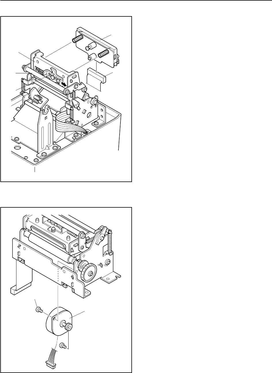
5. Power Unit
(1) Disconnect the power cord from the AC outlet.
(2) Remove:
•Upper casing unit (See 1. above.)
•Three screws (See 4. above.)
•Interface PCB (See 4. above.)
•Screw 1
•Four screws 2
•Lower casing chassis 3
•Connector 4
•Two tapping screws 5
•Shield chassis (A) 6
•Connector 7
•Four screws 8
•Power unit 9
•Screw 0
•Earth plate (A) A
6. Fuse
(1) Remove shield chassis A, according to procedure
given in 5. above.
(2) Check fuse F1. 1
If the fuse is blown, replace with the following.
AC Voltage F1
120V 5TT5A-125V
220-240V EAK3.15A250V
If the replacement fuse also blows out, replace the
power unit or check the main logic board.
6
8
2
1
9
8
78
5
4
3
2
0
A
1
PARTS REPLACEMENT
– 40 –
7. Printhead unit
(1) Remove the upper casing unit. (See 1. above.)
(2) Pull the pressure stay 1 forward to open the head
frame unit 2.
(3) Slide the head clamp 3 in the direction indicated by
the arrow. Remove the printhead unit 4.
(4) Remove the head connector 5.
Note : Be careful to avoid damaging the heat elements
when installing the replacement unit.
8. Feed Motor Assembly
(1) Remove:
•Printer mechanism (See 3. above.)
•Two tapping screws 1
•Feed motor assembly 2
4
5
2
1
3
2
1
PARTS REPLACEMENT
– 41 –
9. Detectors
(1) Remove:
•Printer mechanism (See 3. above.)
•Two screws 1
•Paper-out and black-mark detectors 2
•Tapping screw 3
•Head-up detector 4
10. Label sensor
(1) Remove:
•Two E-rings 1
•Two oiless bushings 2
•Support stay 3
•One tapping screw 4
•Label sensor 5
3
2
1
4
1
2
45
3
12

PARTS REPLACEMENT
– 42 –

CHAPTER 4
MAINTENANCE AND LUBRICATION
1. Maintenance ........................................................................................................ 45
1-1. Cleaning ................................................................................................................. 45
1-2. Checks ................................................................................................................... 45
2. Lubrication........................................................................................................... 46
2-1. Lubricants.............................................................................................................. 46
2-2. Application Method ............................................................................................... 46
2-3. Lubrication Points................................................................................................. 46
4

– 44 –
MAINTENANCE AND LUBRICATION

– 45 –
MAINTENANCE AND LUBRICATION
1. Maintenance
Proper maintenance is necessary to maintain printer performance and forestall potential problems. Please carry out
maintenance as described below.
1-1. Cleaning
(1) Surface dirt
Clear away dirt with a soft cloth. If necessary, apply a small quantity of alcohol to the cloth to improve cleaning
power. NEVER use thinner, trichlene, or ketone solvents, as these can cause damage to plastic components.
When cleaning, take care to avoid damaging or moistening of electronic parts, mechanical parts, and wires.
(2) Internal dust
For best results, use an electric vacuum cleaning device to remove dust from the inside of the printer. Note that such
cleaning may also remove lubrication; when you have finished cleaning, check lubrication levels and apply
lubricant as necessary.
1-2. Checks
There are two types of maintenance checks. Simple “daily checks” can be performed by users during the course of daily
operation. “Periodic checks” must be carried out by qualified service personnel.
(1) Daily checks
• Check whether dirt or other foreign matter has worked its way into the printer, and remove as necessary.
• Check the thermal head for excessive dirt. If the head is very dirty, clean it with a cotton stick or a soft cloth soaked
in alcohol.
(2) Periodic checks
Periodic checks and lubrication should be carried out once every six months or once every million lines of printing.
• Check the integrity of springs.
• Clear dust from areas around the detectors.
MAINTENANCE AND LUBRICATION
– 46 –
MAINTENANCE AND LUBRICATION
2. Lubrication
Proper lubrication is essential for maintaining the printer’s performance level and preventing breakdowns or other
problems.
2-1. Lubricants
Choice of lubrication can significantly affect the printer’s performance, longevity, and low-temperature characteristics.
We recommend the following lubricant for the TSP400 series.
Type Name Manufacturer
Grease Molykote EM Dow Corning
2-2. Application Method
If you are lubricating parts during disassembly or reassembly, be sure to wash or wipe the parts thoroughly to remove all
dirt and dust prior to lubricating.
Remember that cleaning can remove necessary lubrication. Always lubricate after cleaning, disassembly, or replacement.
2-3. Lubrication Points
Apply lubricants at the following locations. (Refer to Diagram 4-1.)
No. Location
1 Contact area of pressure bar and pressure pin
2 Contact area of gear 15×50×0.5 and gear shaft
3 Contact area of gear 58×0.5 and gear shaft
4 Contact area of gear 15×50×0.5 and PF motor gear
5 Contact area of gear 58×0.5 and platen gear
6 Contact area of head stay and head base frame
7 Contact area of head clamp and clamp pin
8 Contact area of head clamp and head stay R
9 Contact area of lever and lever shaft (TSP442)
Note 1 : Paper debris on cutter blade can cause paper jams. Clean away debris by wiping with alcohol, then reapply
lubricant.
– 47 –
MAINTENANCE AND LUBRICATION
Fig. 4-1 Lubrication Points
A
C
D
D
B
1
8
7
1
6
6
3
4
2
9
9
5
A
B
C

– 48 –
MAINTENANCE AND LUBRICATION

CHAPTER 5
PARTS LIST
READING THE LISTS
(1) DRWG. NO.
Corresponds to the drawing number or to the silk-screened number on the board to which the part is mounted.
(2) REVISED EDITON MARK
This column shows a revision number.
Parts that have been added in the revised edition are indicated with “#”.
Parts that have been abolished in the revised edition are indicated with “*”.
#1 : First edition → Second edition #2 : Second edition → Third edition
*1 : First edition → Second edition *2 : Second edition → Third edition
(3) PART NO.
Part identification number. Always indicate this number clearly when ordering a part.
Parts described as “NPN” have no parts number and are not in stock, i.e., unavailable.
(4) PART NAME
Name of part. Always include the name (as well as the part No.) when ordering the part.
(5) QTY
Indicates the number of units of the part used within the assembly.
(6) REMARKS
This column is used for general comments. It also indicates EPROM seal numbers. A “*” within a seal number
indicates the version number.
(7) RANK
“S” indicates that the part is a “service part” that should always be kept in stock for maintenance purposes.
1. Printer Assembly.............................. 50
1-1. Disassembly Drawing ................... 50
A. TSP412D ....................................50
B. TSP442D ....................................51
1-2. Parts List ......................................... 52
2. Printer Mechanism Assembly ......... 54
2-1. Disassembly Drawing ................... 54
2-2. Parts List ......................................... 55
3. Connector Wiring Diagram.............. 56
A. RS-232C Interface Type .............. 56
B. RS-422A Interface Type .............. 57
C. Parallel Interface Type ................ 58
4. Main Logic Board ............................. 59
4-1. Circuit Diagram...............................59
4-2. Parts List ......................................... 63
5. RS232C Interface Board .................. 66
5-1. Circuit Diagram...............................66
5-2. Parts List ......................................... 67
6. RS422A Interface Board .................. 68
6-1. Circuit Diagram...............................68
6-2. Parts List .........................................69
7. Centronics Interface Board ............. 70
7-1. Circuit Diagram...............................70
7-2. Parts List .........................................71
8. Control Panel Board ........................ 72
8-1. Circuit Diagram...............................72
8-2. Parts List .........................................73
9. Paper-Out Detector Board ............... 74
9-1. Circuit Diagram...............................74
9-2. Parts List .........................................74
10. Label Sensor Board ......................... 74
10-1.Circuit Diagram...............................74
10-2.Parts List .........................................74
5
– 50 –
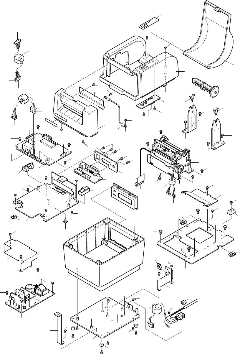
1. Printer Assembly
1-1. Disassembly Drawing
A. TSP412D
LC
EDF
K
M
O
R
PN
Q
O
Q
R
T
J
G
H
A
I
T
M
C
D
EF
G
I
H
A
B
J
18
48
47
13
12
710
3
2
1
33
9
45
45
8
44
4
5
51
54
49
6
49
749
7
19
50
42
42
42
21
50
7
16
12
57
14 15
56
39
28
42
22
22
24
32
23 23
25
26
57
43
27
29
48
59
58
31
53
47
60
30 57
39 58
42
41
46
49 40
47
57
41
K
17
B
20 54
55
L
N
P
41
– 51 –
B. TSP442D
5
C
56
58
LSC
EDF
K
S
M
O
N
P
R
L
PN
Q
O
Q
R
T
G
H
A
I
T
M
DG
I
H
A
B
18
29
48
47
53
47
48
13
12
710
3
2
1
33
44
9
45
45
54
8
44
4
51
41
49
6
49
46
749
7
19
50
42
42
20
42
21
50
7
47 57
16
49
12
14 15
40
57
52
48
39
58
58
60
35
34
42
22
22
24
32
23 23
25
26
57
45
27
50
28
52
37
38
52
36
K
17
41
B
54
55
EF
56
41

– 52 –
1 87391070 LOWER CASE CHASSIS UNIT BCP4 1
2 87393030 POWER SUPPLY UNIT SLS-060P-50 1 US S
87393090 POWER SUPPLY UNIT SLS060PH-50A 1 EC,UK S
3 82011481 SHIELD CHASSIS A BCP4 1
4 87393040 CORD SET UNIT US BCP4 1 US S
87393070 CORD SET UNIT EC BCP4 1 EC S
87393080 CORD SET UNIT UK BCP4 1 UK S
5 04991220 CORD BUSHING SR-5N-4 1
6 82011490 SHIELD CHASSIS B BCP4 1
7 04991254 CORD CLAMP EDS-1208U 4 S
8 80991601 RUBBER FOOT 8340 4 S
9 87391080 LOWER CASE UNIT BCP4 1
10 NPN BOARD CHASSIS TSP4 1
12 33750010 BOARD RAIL TSP4 2
13 37407000 MAIN LOGIC BOARD UNIT TSP4 1 S
14 *2 37403800 IF PLATE RS232 UNIT TSP4 1 RS232C S
#2 37407800 RS232C IF BOARD UNIT TSP4 1 RS232C S
37407810 RS422 IF BOARD UNIT TSP4 1 RS422A S
37407820 PARALLEL IF BOARD UNIT TSP4 1 PARALLEL S
15 32021010 SERIAL IF PLATE TSP4 1 RS232C,RS422A
32021110 PARALLEL IF PLATE TSP4 1 PARALLEL
16 33020200 INTERFACE COVER TSP4 1
17 30721030 CABLE UNIT 12X220CC TSP4 1
18 30721021 CABLE UNIT B TSP4 1 EC,UK
30721040 CABLE UNIT A TSP4 1 US
19 32010211 MECHANISM BASE CHASSIS TSP4 1
20 *2 32912010 ROM COVER TSP4 1
#2 32912011 ROM COVER TSP4 1
21 38405000 TMP412-24 1 S
22 32041010 HOLDER ANGLE TSP4 2
23 83201000 ROLL PAPER BUSHING BMP4 2 S
24 83903931 LABEL HOLDER 3.25 BMP4 1 ACCESSORY S
25 83025392 UPPER CASE BCP4 2
26 87390610 CONTROL PANEL BOARD ASSY BCP4 1 S
27 30061010 OPERATION SHEET TSP4 1
28 83025420 FRONT COVER A BCP4 1 TSP412
83025481 FRONT COVER B BCP4 1 TSP442
29 30071010 BRAND SEAL TSP4 1
30 82902290 CUTTER BCP4 1 TSP412 S
31 80701770 WIRE 18UL1007BRN145TT 1 TSP412
32 33020210 UPPER COVER B TSP4 1 S
33 32790000 EARTH PLATE A TSP4 1
34 80040151 CUTTER 4010 BCP4 1 TSP442 S
35 82902430 CUTTER HOLDER BCP4 1 TSP442
36 82040621 CUTTER PAPER GUIDE B BCP4 1 TSP442
37 82902460 PAPER GUIDE CLAMP BCP6 1 TSP442
38 82040611 CUTTER PAPER GUIDE A BCP4 1 TSP442
39 04991401 SCREW DBLC-J25SAF 2 RS232C,RS422A S
40 09990527 BOARD SPACER RSPS-8L 1 S
41 09990723 FERRITE CORE TFC-23-11-14 2 US
09990723 FERRITE CORE TFC-23-11-14 3 EC,UK
42 01903077 SCREW TAT 3-5 CT-FL 10 TSP412 S
01903077 SCREW TAT 3-5 CT-FL 11 TSP442 S
43 00930605 SCREW TAT 3-6 FS 2 S
44 00930609 SCREW TAT 3-6 CT 4 S
1-2. Parts List Printer Assembly
DRWG.NO. REV. PARTS NO. PARTS NAME Q'TY REMARKS RANK

– 53 –
45 00930803 SCREW TAT 3-8 PT 6 S
46 01903018 SCREW TR 3-6 WS/WF 4 S
47 01903059 SCREW TR 3-5 FL 6 S
48 01903069 SCREW TAT 3-5 ST-FL 2 TSP412 S
01903069 SCREW TAT 3-5 ST-FL 4 TSP442 S
49 01903099 SCREW TR 3-4 WS 5 S
50 01914035 SCREW TAT 4-10 PT-FL 4 S
51 01914036 SCREW TR 4-5 WS 1 S
52 00630404 SCREW TR 3-4 7 TSP442 S
53 00930803 SCREW TAT 3-8 PT 2 S
54 #1 00930500 SCREW TAT 3-5 ST 2 S
55 #1 04991257 CORE STOPPER TFP2014-V 1
56 #2 09990713 FERRITE CORE TRCC-16-8-16 CASE 2 EC,UK
57 #2 00930603 SCREW TAT 3-6 PT 6 TSP412 S
#2 00930603 SCREW TAT 3-6 PT 4 TSP442 S
58 #2 00630504 SCREW TR 3-5 3 S
59 #2 01903085 SCREW TAT 3-7 WS 1 TSP412 S
60 #2 30091010 TENSION SHEET TSP2 1
- #2 09990723 FERRITE CORE TFC-23-11-14 1 ACCESSORY :EC
#2 09990728 FERRITE CORE TFC-20-10-10 1 ACCESSORY :EC
#2 04991204 FASTENER T18S 1 ACCESSORY :EC
Printer Assembly
DRWG.NO. REV. PARTS NO. PARTS NAME Q'TY REMARKS RANK
– 54 –
2. Printer Mechanism Assembly
2-1. Disassembly Drawing
15-6 15-10
15-16
15-13 15-14
15-5
15-4
15-3
15-11
15
15-9
29
29
25
15-9
15-15
15-2
15-1
15-6
15-10
15-16
15-13
15-12
15-7
15-14
15-8
15-14
15-14
15-7
15-12
15-13
15-17
11
9
10
40
6
13
33
33
33
5
37 33
8
1
2432
13
33
8
7
30
431
38 3
12
41
39
2
39
B
A
C
D
D
15-13
45
44
A
B
24
32
14
C
34
43

– 55 –
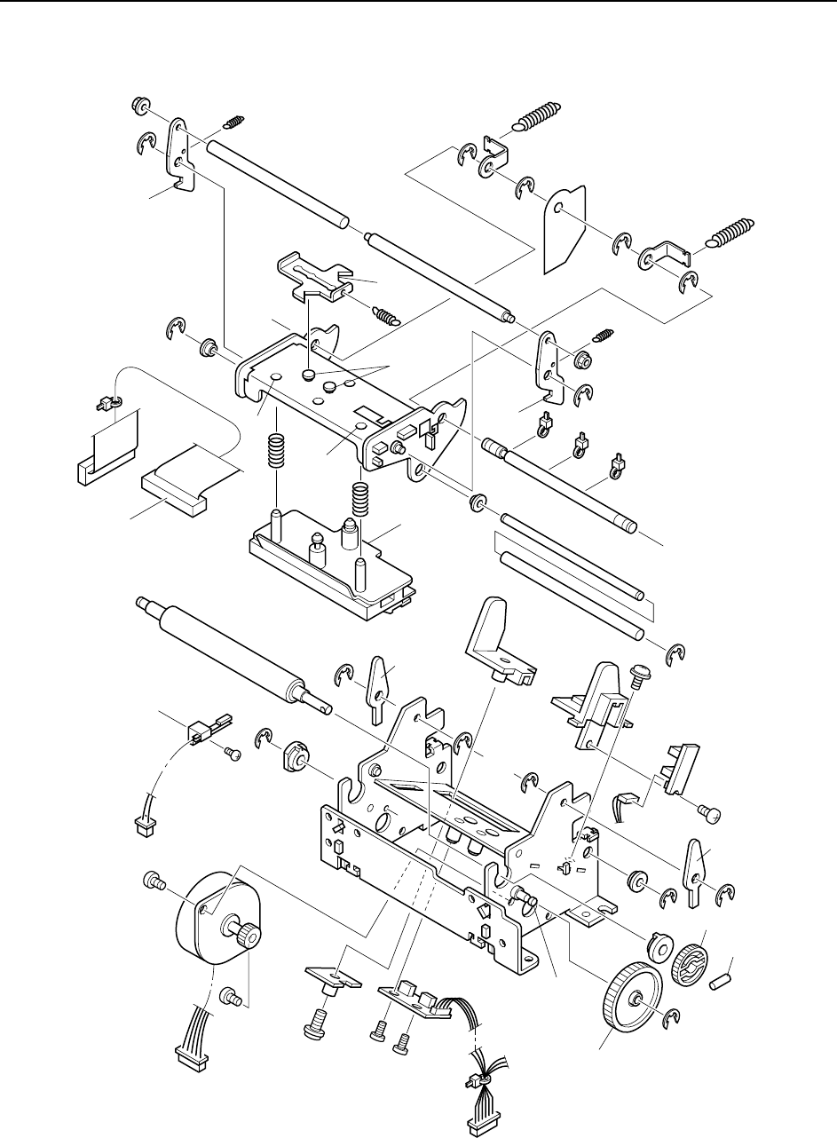
1 NPN FRAME ASSY 1
2 37412300 PF MOTOR ASSY TMP4 1 S
3 37417000 REFLECT SENSOR BD UNIT TMP4 1 S
4 83100460 IDLER GEAR 15X50X0.5 1 S
5 87340390 HEAD DETECTOR ASSY BMP8 1 S
6 *2 31375210 PLATEN TMP4 1 S
#2 31375211 PLATEN TMP4 1 S
7 33102210 GEAR 28X0.5 TMP4 1 S
8 80203041 DRIVE SHAFT BEARING MP300 2 S
9 33910020 PAPER GUIDE A TMP4 1 S
10 37417010 TRANSMIT SENSOR BD UNIT TMP4 1 S
11 *1 33910030 PAPER GUIDE B TMP4 1 S
#1 33910031 PAPER GUIDE B TMP4 1 S
12 33903010 FRICTION PLATE TMP4 1 S
13 33490010 HEAD POSITION LEVER TSP4 2
14 *1 87343110 HEAD UNIT BMP4 1 S
#1 37419000 HEAD UNIT TMP4 1 S
15 *1 87340410 HEAD FRAME UNIT BMP4 1
#1 37410010 HEAD FRAME UNIT TMP4 1
15-1 81360850 PAPER GUIDE ROLLER BMP4 1
15-2 31303010 HEAD UNIT PIVOT SHAFT TSP4 1
15-3 82902330 HEAD CLAMP BMP4 1
15-4 81370910 PRESSURE STAY BMP4 1
15-5 09991391 HEAT-SHRINK TUBE A-6.0 GRN 1
15-6 82401370 PRESSURE LEVER BMP4 2
15-7 82401360 HEAD STOPPER LEVER BMP4 2
15-8 80994252 GUARD SHEET BMP4 1
15-9 04310401 OILESS BUSHING F4X7X3 2
15-10 80511070 SPRING E040-040-0159 2 S
15-11 80510840 SPRING E055-060-0180 1 S
15-12 *1 80511060 SPRING E060-060-0316 2 S
#1 30510410 SPRING E065-070-0238 2 S
15-13 04020015 STOP RING SE3.0 2 S
15-14 04020016 STOP RING SE4.0 2 S
15-15 04991204 FASTENER T18S 3 S
15-16 02040301 FLANGED NUT NHW3 2 S
15-17 09991372 HEAT-SHRINK TUBE 4.0 1 S
25 *1 80705030 CABLE UNIT 26X265CC BMP4 1
#1 80705031 CABLE UNIT 26X290CC BMP4 1
29 *1 80520950 SPRING C075-080-0187 2 S
#1 30520210 SPRING C075-080-0165 2 S
30 04012003 ROLL PIN SP2.0X8 1 S
31 04020010 STOP RING SE2.0 1 S
32 04020015 STOP RING SE3.0 2
33 04020016 STOP RING SE4.0 7
34 04991204 FASTENER T18S 2
37 00920503 SCREW TAT 2-5 CT 1 S
38 00630404 SCREW TR 3-4 2
39 00930403 SCREW TAT 3-4 CT 2
40 00930803 SCREW TAT 3-8 PT 1
41 01914035 SCREW TAT 4-10 PT-FL 1
42 00930609 SCREW TAT 3-6 CT 1
43 30721010 CABLE UNIT TMP4 1
44 #1 01903090 SCREW TAT 3-8 CT-FL 1
45 #1 31361010 SUPPORT STAY TMP4 1
2-2. Parts List Printer Mechanism
DRWG.NO. REV. PARTS NO. PARTS NAME Q'TY REMARKS RANK
– 56 –
3. Connector Wiring Diagram
A. RS-232C Interface Type
1
2
3
4
5
6
7
8
9
10
11
12
13
14
15
16
17
18
19
20
21
22
23
24
25
A1
A2
A3
A4
A5
A6
A7
A8
A9
A10
A11
A12
A13
A14
A15
A16
A17
A18
A19
A20
B1
B2
B3
B4
B5
B6
B7
B8
B9
B10
B11
B12
B13
B14
B15
B16
B17
B18
B19
B20
1
2
3
4
5
6
1
2
3
4
5
6
PERIPHERAL UNIT
CN2
CN3
RS232C I/F BOARD
F-GND
TXD
RXD
RTS
CTS
NC
GND
NC
NC
NC
RCH
NC
GND
FAULT
MP-TXD
MP-DTR
NC
NC
NC
DTR
NC
NC
NC
NC
NC
NC
NC
VVR
DIN1
DIN3
DIN5
DIN7
GND
Vcc(+5V)
NC
NC
NC
DIEN
GND
RXD
NC
ID2
GND
PEXT1
VEXT
NC
NC
GND
DIN2
DIN4
DIN6
DIN8
GND
Vcc(+5V)
NC
FAULT
DTR
GND
TXD
CTS
ID1
GND
PSWIN
PEXT2
VEXT
DIN9
DIN11
VVR
DIN1
DIN3
DIN5
DIN7
GND
Vcc(+5V)
ERR
SLCT
BUSY
STB
GND
RXD
ID0
ID2
GND
PEXT1
VEXT
DIN10
DIN12
GND
DIN2
DIN4
DIN6
DIN8
GND
Vcc(+5)
NMI
PE
ACK
GND
TXD
CTS
ID1
GND
PSWIN
PEXT2
VEXT
1
2
3
4
5
6
7
1
2
1
2
3
4
5
6
1
2
3
4
1
2
3
GND
PE
MARK
Vcc(+5)
LABLE
GND
LED
HUP DTCT
HUP DTCT
LFCMN
LFCMN
LFø1
LFø3
LFø4
LFø2
1
2
3
4
5
6
7
8
9
10
11
12
13
14
15
16
17
18
19
20
21
22
23
24
25
26
1
2
3
4
1
2
3
4
5
1
2
3
4
5
6
7
8
9
10
11
12
13
14
15
16
17
18
19
20
21
22
23
24
25
26
COM(+24V)
COM(+24V)
COM(+24V)
GND
GND
GND
SI
SO
CLK
GND
LAT
GND
STB5
V
DD
(+5V)
STB3
STB4
STB1
STB2
TM1
TM2
GND
GND
GND
COM(+24V)
COM(+24V)
COM(+24V)
CUTSW
CUTSW
M(–)
M(+)
VP(+24V)
VP(+24V)
NC
P-GND
P-GND
F-GND
PEXT1
VEXT
VEXT
PEXT2
PSW
1
2
3
4
5
1
2
3
4
5
6
7
8
9
10
11
12
1
2
3
4
5
6
7
8
9
10
11
12
OPERATION PANEL
CN1
MAGNET
CORE
(1 TURN)
[CN8]
CN7
Vcc(+5V)
PEXT1
VP(+24V)
PSWIN
GND
GND
COPEN
PF-SW
OL-SW
PSW1
PSW2
PSW
OL-LED
PO-LED
HU-LED
ER-LED
Vcc(+5V)
1
2
3
4
1
2
3
4
5
L
NC
N
NC
FG
POWER SUPPLY UNIT
MAGNET
CORE
(1 TURN)
CUTTER UNIT
CN1
CONTROL BOARD PRINTER MECHANISM
CN9 CN1 CN1
CN1
MARK
DETECTOR PAPER OUT
DETECTOR
LABEL DETECTOR
HADE UP DETECTOR
PAPER FEED MOTOR
ø1
ø3
ø2 ø4
M
THERMAL HEAD
M
CN2
CN4
CN6
CN5
CN3 CN1CN2
A1
A2
A3
A4
A5
A6
A7
A8
A9
A10
A11
A12
A13
A14
A15
A16
A17
A18
A19
A20
B1
B2
B3
B4
B5
B6
B7
B8
B9
B10
B11
B12
B13
B14
B15
B16
B17
B18
B19
B20
MAGNET
CORE
(1 TURN)
(TSP442 Series only)
[CN8] is not connected yet.
– 57 –
B. RS-422A Interface Type
1
2
3
4
5
6
7
8
9
10
11
12
13
14
15
16
17
18
19
20
21
22
23
24
25
A1
A2
A3
A4
A5
A6
A7
A8
A9
A10
A11
A12
A13
A14
A15
A16
A17
A18
A19
A20
B1
B2
B3
B4
B5
B6
B7
B8
B9
B10
B11
B12
B13
B14
B15
B16
B17
B18
B19
B20
1
2
3
4
5
6
1
2
3
4
5
6
PERIPHERAL UNIT
CN2
CN3
RS422A I/F BOARD
F-GND
NC
NC
NC
NC
NC
GND
NC
SD(+)
SD(–)
NC
NC
GND
FAULT
NC
NC
RD(+)
RD(–)
CS(+)
NC
NC
NC
CS(–)
RS(+)
RS(–)
DIN9
DIN11
VVR
DIN1
DIN3
DIN5
DIN7
GND
Vcc(+5V)
DOEN
NC
NC
DIEN
GND
RD
ID0
ID2
GND
PEXT1
VEXT
DIN10
DIN12
GND
DIN2
DIN4
DIN6
DIN8
GND
Vcc(+5V)
NC
FAULT
RS
GND
SD
CS
ID1
GND
PSWIN
PEXT2
VEXT
DIN9
DIN11
VVR
DIN1
DIN3
DIN5
DIN7
GND
Vcc(+5V)
ERR
SLCT
BUSY
STB
GND
RXD
ID0
ID2
GND
PEXT1
VEXT
DIN10
DIN12
GND
DIN2
DIN4
DIN6
DIN8
GND
Vcc(+5)
NMI
PE
ACK
GND
TXD
CTS
ID1
GND
PSWIN
PEXT2
VEXT
1
2
3
4
5
6
7
1
2
1
2
3
4
5
6
1
2
3
4
1
2
3
GND
PE
MARK
Vcc(+5)
LABLE
GND
LED
HUP DTCT
HUP DTCT
LFCMN
LFCMN
LFø1
LFø3
LFø4
LFø2
1
2
3
4
5
6
7
8
9
10
11
12
13
14
15
16
17
18
19
20
21
22
23
24
25
26
1
2
3
4
1
2
3
4
5
1
2
3
4
5
6
7
8
9
10
11
12
13
14
15
16
17
18
19
20
21
22
23
24
25
26
COM(+24V)
COM(+24V)
COM(+24V)
GND
GND
GND
SI
SO
CLK
GND
LAT
GND
STB5
VDD(+5V)
STB3
STB4
STB1
STB2
TM1
TM2
GND
GND
GND
COM(+24V)
COM(+24V)
COM(+24V)
CUTSW
CUTSW
M(–)
M(+)
VP(+24V)
VP(+24V)
NC
P-GND
P-GND
F-GND
PEXT1
VEXT
VEXT
PEXT2
PSW
1
2
3
4
5
1
2
3
4
5
6
7
8
9
10
11
12
1
2
3
4
5
6
7
8
9
10
11
12
OPERATION PANEL
CN1
MAGNET
CORE
(1 TURN)
[CN8]
CN7
Vcc(+5V)
PEXT1
VP(+24V)
PSWIN
GND
GND
COPEN
PF-SW
OL-SW
PSW1
PSW2
PSW
OL-LED
PO-LED
HU-LED
ER-LED
Vcc(+5V)
1
2
3
4
1
2
3
4
5
L
NC
N
NC
FG
POWER SUPPLY UNIT
MAGNET
CORE
(1 TURN)
CUTTER UNIT
CN1
CONTROL BOARD PRINTER MECHANISM
CN9 CN1 CN1
CN1
MARK
DETECTOR PAPER OUT
DETECTOR
LABEL DETECTOR
HADE UP DETECTOR
PAPER FEED MOTOR
ø1
ø3
ø2 ø4
M
THERMAL HEAD
M
CN2
CN4
CN6
CN5
CN3 CN1CN2
A1
A2
A3
A4
A5
A6
A7
A8
A9
A10
A11
A12
A13
A14
A15
A16
A17
A18
A19
A20
B1
B2
B3
B4
B5
B6
B7
B8
B9
B10
B11
B12
B13
B14
B15
B16
B17
B18
B19
B20
MAGNET
CORE
(1 TURN)
(TSP442 Series only)
[CN8] is not connected yet.
– 58 –
C. Parallel Interface Type
1
2
3
4
5
6
7
8
9
10
11
12
13
14
15
16
17
18
19
20
21
22
23
24
25
26
27
28
29
30
31
32
33
34
35
36
A1
A2
A3
A4
A5
A6
A7
A8
A9
A10
A11
A12
A13
A14
A15
A16
A17
A18
A19
A20
B1
B2
B3
B4
B5
B6
B7
B8
B9
B10
B11
B12
B13
B14
B15
B16
B17
B18
B19
B20
1
2
3
4
5
6
1
2
3
4
5
6
PERIPHERAL UNIT
CN2
CN3
PARALLEL I/F BOARD
STROBE
DATA 1
DATA 2
DATA 3
DATA 4
DATA 5
DATA 6
DATA 7
DATA 8
ACK
BUSY
PE
SLCT
NC
NC
GND
F-GND
Vcc(+5V)
RETURN-GND
RETURN-GND
RETURN-GND
RETURN-GND
RETURN-GND
RETURN-GND
RETURN-GND
RETURN-GND
RETURN-GND
RETURN-GND
RETURN-GND
RETURN-GND
INIT
ERROR
EXT-GND
CPL
NC
SLCT-IN
NC
NC
VVR
DIN1
DIN3
DIN5
DIN7
GND
Vcc(+5V)
ERROR
SLCT
BUSY
STB
GND
NC
ID0
NC
GND
PEXT1
VEXT
NC
NC
GND
DIN2
DIN4
DIN6
DIN8
GND
Vcc(+5V)
INIT
PE
ACK
GND
NC
NC
ID1
GND
PSWIN
PEXT2
VEXT
DIN9
DIN11
VVR
DIN1
DIN3
DIN5
DIN7
GND
Vcc(+5V)
ERR
SLCT
BUSY
STB
GND
RXD
ID0
ID2
GND
PEXT1
VEXT
DIN10
DIN12
GND
DIN2
DIN4
DIN6
DIN8
GND
Vcc(+5)
NM1
PE
ACK
GND
TXD
CTS
ID1
GND
PSWIN
PEXT2
VEXT
1
2
3
4
5
6
7
1
2
1
2
3
4
5
6
1
2
3
4
1
2
3
GND
PE
MARK
Vcc(+5)
LABLE
GND
LED
HUP DTCT
HUP DTCT
LFCMN
LFCMN
LFø1
LFø3
LFø4
LFø2
1
2
3
4
5
6
7
8
9
10
11
12
13
14
15
16
17
18
19
20
21
22
23
24
25
26
1
2
3
4
1
2
3
4
5
1
2
3
4
5
6
7
8
9
10
11
12
13
14
15
16
17
18
19
20
21
22
23
24
25
26
COM(+24V)
COM(+24V)
COM(+24V)
GND
GND
GND
SI
SO
CLK
GND
LAT
GND
STB5
VDD(+5V)
STB3
STB4
STB1
STB2
TM1
TM2
GND
GND
GND
COM(+24V)
COM(+24V)
COM(+24V)
CUTSW
CUTSW
M(–)
M(+)
VP(+24V)
VP(+24V)
NC
P-GND
P-GND
F-GND
PEXT1
VEXT
VEXT
PEXT2
PSW
1
2
3
4
5
1
2
3
4
5
6
7
8
9
10
11
12
1
2
3
4
5
6
7
8
9
10
11
12
OPERATION PANEL
CN1
MAGNET
CORE
(1 TURN)
[CN8]
CN7
Vcc(+5V)
PEXT1
VP(+24V)
PSWIN
GND
GND
COPEN
PF-SW
OL-SW
PSW1
PSW2
PSW
OL-LED
PO-LED
HU-LED
ER-LED
Vcc(+5V)
1
2
3
4
1
2
3
4
5
L
NC
N
NC
FG
POWER SUPPLY UNIT
MAGNET
CORE
(1 TURN)
CUTTER UNIT
CN1
CONTROL BOARD PRINTER MECHANISM
CN9 CN1 CN1
CN1
MARK
DETECTOR PAPER OUT
DETECTOR
LABEL DETECTOR
HADE UP DETECTOR
PAPER FEED MOTOR
ø1
ø3
ø2 ø4
M
THERMAL HEAD
M
CN2
CN4
CN6
CN5
CN3 CN1CN2
A1
A2
A3
A4
A5
A6
A7
A8
A9
A10
A11
A12
A13
A14
A15
A16
A17
A18
A19
A20
B1
B2
B3
B4
B5
B6
B7
B8
B9
B10
B11
B12
B13
B14
B15
B16
B17
B18
B19
B20
MAGNET
CORE
(1 TURN)
[CN8] is not connected yet.
– 59 –
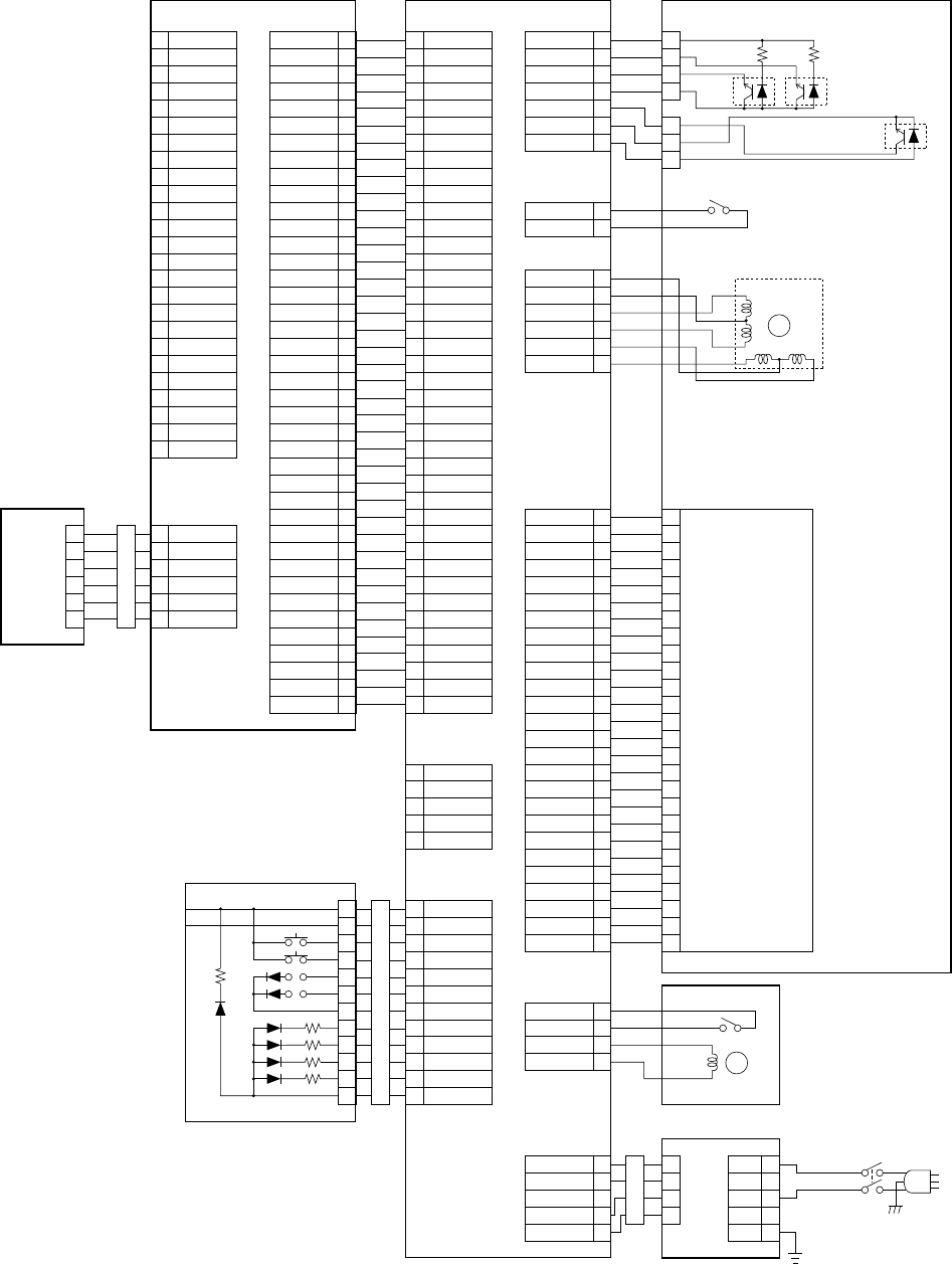
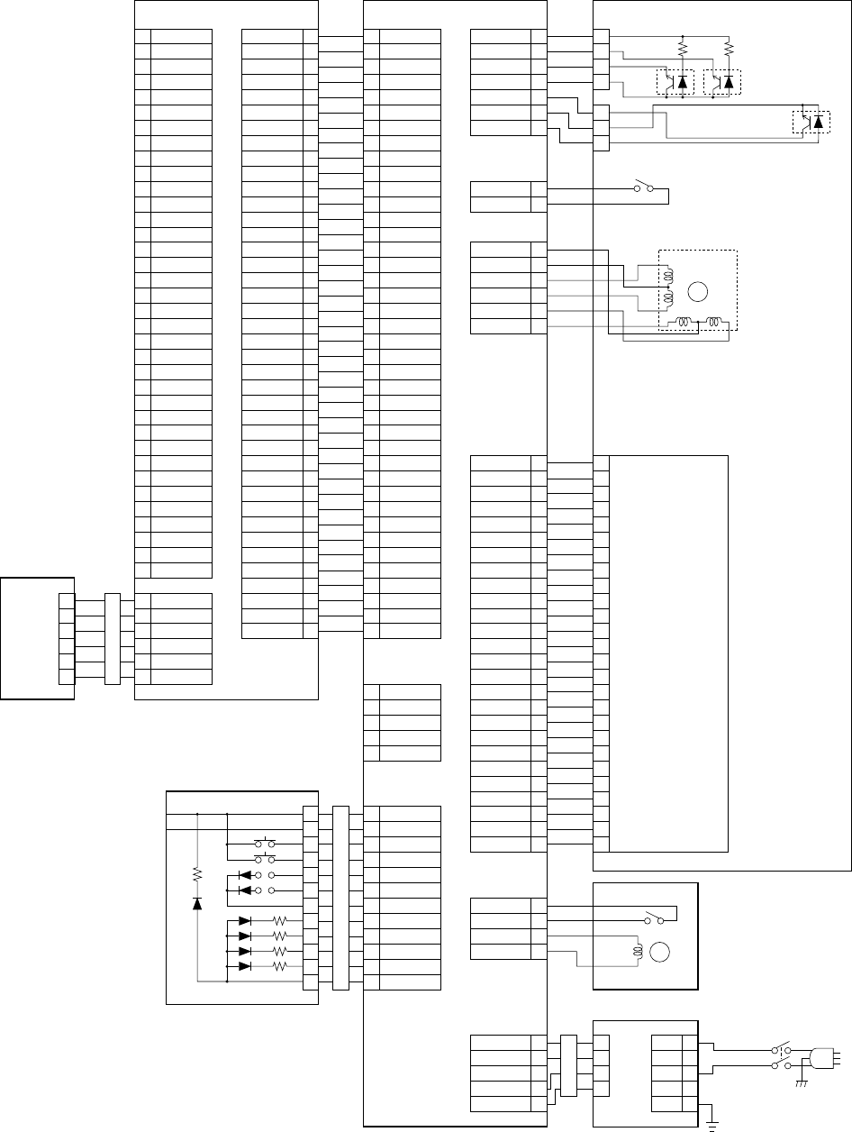
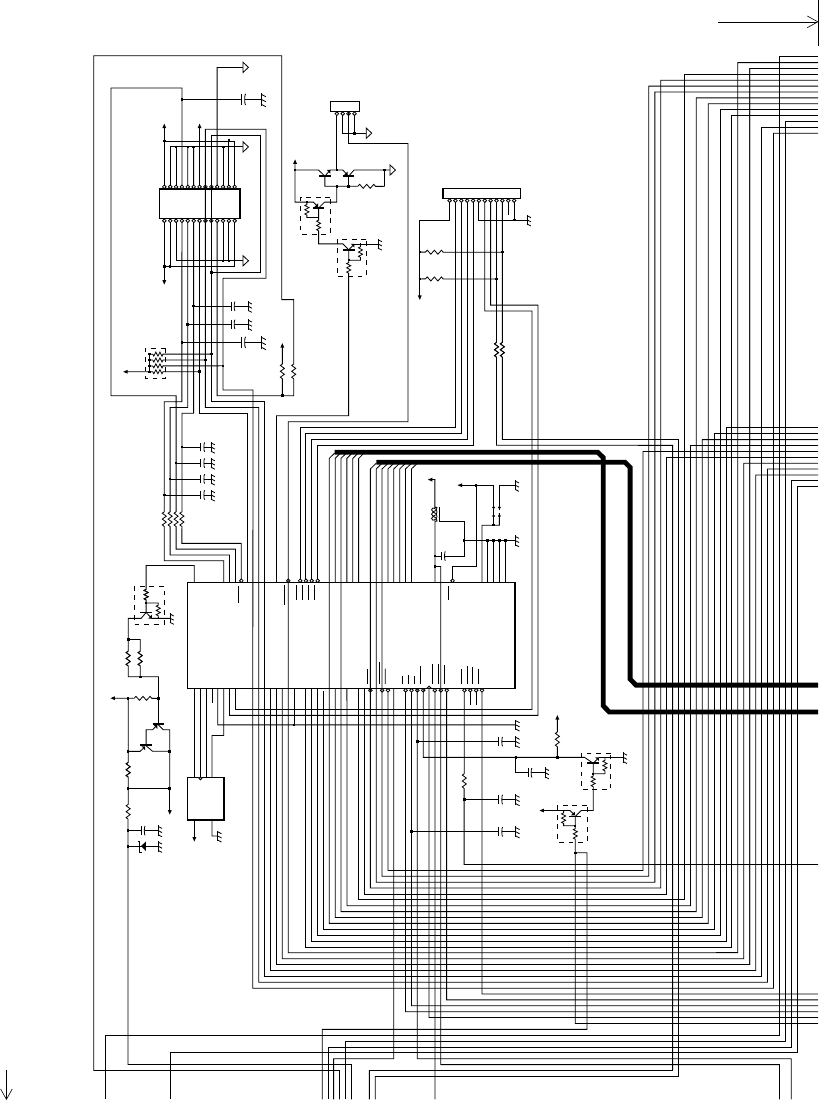
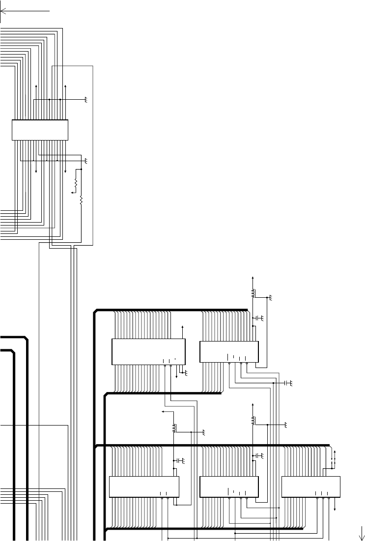
4. Main Logic Board
4-1. Circuit Diagram
ZD2
RD4. 7JSB1 R25
10K R120
10K
C134
0.1U
Q4
A1649
R119
10K
VP
Q5
A1388
R17
10K
R124
10K
DQ5
FA1A4P
VH
VCC 8
5
IC8
VCC
GND
CS
SK
DI
DO
1
2
3
4
93C46
R18
33
C9
33P C126
33P
C127
100P
C8
33P
R19
10K VCC
DQ6
FA1A4P
DQ7
FN1A4P
VCC
32
31
30
29
28
27
26
25
24
23
22
21
20
19
18
17
1
2
3
4
5
6
7
8
9
10
11
13
14
15
41
57
56
55
52
54
16
51
60
63
61
62
59
47
I/O1
I/O2
I/O3
I/O4
IN5
IN6
IN7
IN8
HDPWR
IN9
IN10
IN11
IN12
IN13
IN14
IN15
IN16
CD0
CD1
CD2
CD3
CD4
CD5
CD6
CD7
CSTB
ACK
BUSY
ERROR
SELECT
POUT
HDON
RD
WR
CE
RESET
CLK
INTCDT
INTSDT
RAMCS
PSOE
PSCE0
PSCE1
RFSH
UPD65622GF-TSP
SDATA
SCLK
HISTIN
LATCH
STB4
STB3
STB2
STB1
CUTON
CUTSW
OUT1
OUT2
OUT3
OUT4
A0
A1
A2
A3
A15
A17
D0
D1
D2
D3
D4
D5
D6
D7
VCC
VCC
TEST
PSSEL
GND
GND
GND
GND
49
50
46
48
42
43
44
45
40
39
38
37
36
35
69
68
67
66
65
64
79
78
77
76
75
74
73
70
34
72
80
58
12
33
53
71
A0
A1
A2
A3
A15
A17
D8
D9
D10
D11
D12
D13
D14
D15
R21
R20
R23
R22
33 × 4
C129 C131
C128 C130
33P × 4
FL4
TU02M VCC
2
31
C135
0.1U VCC
JPB2
JPA2
5P8128 :
5P832 : Standard
JPB2=Cut, JPA2=Short
R130
4.7K
R131
4.7K
VCC
R129
4.7K R134
4.7K CN7
53014-1210
12
11
10
9
8
7
6
5
4
3
2
1
VCC
ER-LED
HU-LED
PO-LED
OL-LED
PSW
PSW2
PSW1
OL-SW
PF-SW
COPEN
GND
DQ3
FA1A4P
R16
1K
1/2W
DQ4
FN1A4P
VP
Q1
D2010
Q3
B1359
CN5
5483-04A-RED
4
3
2
1
VCC
1
RA1
10K × 4
2435
C123 C120
C121
100P × 3
VH COM
COM
GND
SI
CLK
/LAT
/STB5
/STB3
/STB1
TH1
GND
GND
COM
1
3
5
7
9
11
13
15
17
19
21
23
25
2
4
6
8
10
12
14
16
18
20
22
24
26
COM
GND
GND
SO
GND
GND
VDD
/STB4
/STB2
TH2
GND
COM
COM
CN6
5332-265G1
(AOI : J080-85523)
VH
VCC
C122
100P
THERMAL HEAD BLOCK
R128
20K
R127
1K
VCC
EXPANDED I/O BLOCK
IC10
ASIDE B
C
– 60 –
VCC
VCC
VCCVB
VCC
VCC
VCC
D0
D1
D2
D3
D4
D5
D6
D7
D8
D9
D10
D11
D12
D13
D14
D15
19
18
17
16
15
14
13
12
10
9
8
7
6
5
4
3
2
20
11
30
O0
O1
O2
O3
O4
O5
O6
O7
O8
O9
O10
O11
O12
O13
O14
O15
CE
OE
GND
GND
IC11
A0
A1
A2
A3
A4
A5
A6
A7
A8
A9
A10
A11
A12
A13
A14
A15
A16
A17
VPP
VCC
21
22
23
24
25
26
27
28
29
31
32
33
34
35
36
37
38
39
1
40
A1
A2
A3
A4
A5
A6
A7
A8
A9
A10
A11
A12
A13
A14
A15
A16
A17
A18
(AM27C4096)
AM27C2048
(AM27C1024)
C137
0.1U
FL5
TU02M
13
2
D8
D9
D10
D11
D12
D13
D14
D15
13
14
15
17
18
19
20
21
1
29
24
22
16
D0
D1
D2
D3
D4
D5
D6
D7
RFSH
R/W
OE
CE1
IC6
A0
A1
A2
A3
A4
A5
A6
A7
A8
A9
A10
A11
A12
A13
A14
A15
A16
CE2
12
11
10
9
8
7
6
5
27
26
23
25
4
28
3
31
2
32
30
A1
A2
A3
A4
A5
A6
A7
A8
A9
A10
A11
A12
A13
A14
A15
A16
A17
LH5P8128N
(LH5P832N)
C110
0.1U
FL1
TU02M
13
2
D8
D9
D10
D11
D12
D13
D14
D15
11
12
13
15
16
17
18
19
27
22
20
28
D0
D1
D2
D3
D4
D5
D6
D7
WE
OE
CE
VCC
A0
A1
A2
A3
A4
A5
A6
A7
A8
A9
A10
A11
A12
A13
A14
10
9
8
7
6
5
4
3
25
24
21
23
2
26
1
A0
A1
A2
A3
A4
A5
A6
A7
A8
A9
A10
A11
A12
A14
JPB1
JPA1
A13
(HM62256ALFP)
HM6264LFP 6264:
62256:
Standard
JPA1=Cut, JPB1=Short
D0
D1
D2
D3
D4
D5
D6
D7
D8
D9
D10
D11
D12
D13
D14
D15
14
16
18
20
23
25
27
29
15
17
19
21
24
26
28
30
11
13
32
12
31
O0
O1
O2
O3
O4
O5
O6
O7
O8
O9
O10
O11
O12
O13
O14
O15/A-1
CE
OE
W/B
GND
GND
IC9
A0
A1
A2
A3
A4
A5
A6
A7
A8
A9
A10
A11
A12
A13
A14
A15
A16
A17
A18
A19
VCC
10
9
8
7
6
5
4
3
41
40
39
38
37
36
35
34
33
2
1
42
22
A1
A2
A3
A4
A5
A6
A7
A8
A9
A10
A11
A12
A13
A14
A15
A16
A17
A18
A19
A20
(UPD23C16000)
(UPD23C8000)
UPD23C4000A
D0
D1
D2
D3
D4
D5
D6
D7
13
14
15
17
18
19
20
21
1
29
24
22
16
D0
D1
D2
D3
D4
D5
D6
D7
RFSH
R/W
OE
CE1
A0
A1
A2
A3
A4
A5
A6
A7
A8
A9
A10
A11
A12
A13
A14
A15
A16
CE2
12
11
10
9
8
7
6
5
27
26
23
25
4
28
3
31
2
32
30
A1
A2
A3
A4
A5
A6
A7
A8
A9
A10
A11
A12
A13
A14
A15
A16
A17
LH5P8128N
(LH5P832N)
C111
0.1U
FL2
TU02M
1
2
3
C4
33P
IC7
CN9
PHEC40R-R111
A1
A2
A3
A4
A5
A6
A7
A8
A9
A10
A11
A12
A13
A14
A15
A16
A17
A18
A19
A20
B1
B2
B3
B4
B5
B6
B7
B8
B9
B10
B11
B12
B13
B14
B15
B16
B17
B18
B19
B20
VCC
VEXT VEXT
VCC
VCC
R29
1K
R28
4.7K
COMMUNICATION I/F BLOCK
MEMORY BLOCK
IC1
D
SIDE A B
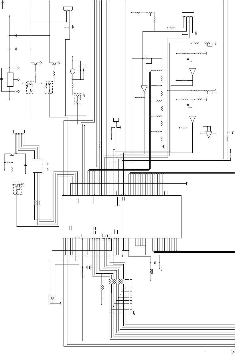
– 61 –
VP
DQ2
FA1A4P
D1
EG01YV0
VCC
R15
10K
R103
10K
Q2
B1359
FEED
MOTOR
CN4
5483-06A
1
2
3
4
5
6
TA1
MP4020
1B
2B
3B
4B
1C
2C
3C
4C
EE
1
01
2
4
6
8
3
5
7
9
R3
R2
R104
R105
3.3K × 4
X1
CST9.83MT
1
3
2
R122
3.3K
C118
0.1U
10K × 2
VCC R9
R6
33 × 9
R10
R8
R7
R5
R4
R12
R13
R14
R123
33P × 9
C105 C103
C104 C102 C106 C108
C101 C107 C119
C11
0.1U
FL3
TU02M
VCC 31
2
C125
0.1U
VCC
D0
D1
D2
D3
D4
D5
D6
D7
D8
D9
D10
D11
D12
D13
D14
D15
20
21
22
23
24
25
75
74
71
81
82
83
100
101
102
103
104
80
79
78
77
72
70
69
68
67
66
1
44
84
76
85
10
26
35
53
99
94
73
27
28
29
30
31
32
33
34
36
37
38
39
40
41
42
43
IC5
P90/TXD0
P91/TXD1
P92/RXD0
P93/RXD1
P94/SCK0/IREQ4
P95/SCK1/IREQ5
XTAL
EXTAL
RES
MD0
MD1
MD2
P80/RFSH/IRQ0
P81/CS3/IRQ1
P82/CS2/IRQ2
P83/CS1/IRQ3
P84/CS0
LWR
HWR
RD
AS
NMI
STBY
CLK
P62/BACK
P61/BREQ
P60/WAIT
VCC
VCC
AVCC
VCC
VREF
VSS
VSS
VSS
VSS
VSS
AVSS
VSS
P40/D0
P41/D1
P42/D2
P43/D3
P44/D4
P45/D5
P46/D6
P47/D7
D8
D9
D10
D11
D12
D13
D14
D15
HD6413003F10T
RESO
PA7/TP7/TIOCB2
PA6/TP6/TIOCA2
PA5/TP5/TIOCB1
PA4/TP4/TIOCA1
PA3/TP3/TIOCB0/
PA2/TP2/TIOCA0/
PA1/TP1/TEND1/T
PA0/TP0/TEND0/T
PB0/TP8/TIOCA3
PB1/TP9/TIOCB3
PB2/TP10/TIOCA4
PB3/TP11/TIOCB4
PB4/TP12/TIOCXA
PB5/TP13/TIOCXB
PB6/TP14/DREQ0
PB7/TP15/DREQ1/
P70/AN0
P71/AN1
P72/AN2
P73/AN3
P74/AN4
P75/AN5
P76/AN6
P77/AN7
PC0
PC1
PC2/TEND2/CS4
PC3/DREQ2/CS5
PC4/TEND3/CS6
PC5/DREQ3/CS7
PC6/IRQ6
PC7/IRQ7
A0
A1
A2
A3
A4
A5
A6
A7
A8
A9
A10
A11
A12
A13
A14
A15
A16
A17
A18
A19
P54/A20
P55/A21
P56/A22
P57/A23
19
112
111
110
109
108
107
106
105
2
3
4
5
6
7
8
9
86
87
88
89
90
91
92
93
11
12
13
14
15
16
17
18
45
46
47
48
49
50
51
52
54
55
56
57
58
59
60
61
62
63
64
65
95
96
97
98
DA0
DA1
DA2
DA3
DA4
@
A0
A1
A2
A3
A4
A5
A6
A7
A8
A9
A10
A11
A12
A13
A14
A15
A16
A17
A18
A19
A20
FEED MOTOR BLOCK
PERIPHERAL/BUZZER BLOCK
R11
1K
R100
10K
VCC CN2
5483-02A
2
1HEAD UP
DETECTOR
SENSERS BLOCK
VCC
VCC
VCC
R136
1K
LABEL
MARK
PE
VR3
4.7K
3
1
2
R31
2.7K
R27
10K
–
+
3
1
2
C14
0.1U
R26
4.7K
IC12-D
13 10
11
UPC339C
6
7
UPC339C
VR4
4.7K
R137
1K
VCC
R33
2.7K
R32
4.7K
C13
0.1U
IC12-B
VCC
1
R30
4.7K
VCC
–
+
–
+
VCC
3
5
4
IC12-A
2
UPC339C 1
–
2
R114
20K
DA4
R115
10K
R113
20K
DA3
R111
10K
R112
20K
DA2
R108
10K
R110
20K
DA1
R107
10K
R109
20K
DA0
R106
20K
8
9
–
+
14
IC12-C
UPC339C
R116
4.7K
C15
0.1U
VCC
VP
DD1
VCC
DQ8
FN1A4P
R132
1K
VCC
DQ9
FN1A4P
R133
1K Q9
D2010
Q8
D2010
VP
D2
1SR139-100
IC3
UPC7824HF
VI VO
G
N
D
C114
0.1U C113
0.1U
D4
1SR139-100 D3
1SR139-100
VCC
BZ +
BZ1
QMB111P
R1
330
DQ1
FA1A4P
DCB010
2
3
1VR2
4.7K
VCC
2
3
1VR1
47K
VCC
R135
220
R101
220
CN1
53014-0710
7
6
5
4
3
2
1
LABEL
MARK
PE
[CN8]
53014-0510
<FOR PRESENTER>
1
2
3
4
5
VEXT
VCC R118
33 C117
33P
R117
10K
CSIDE D
A
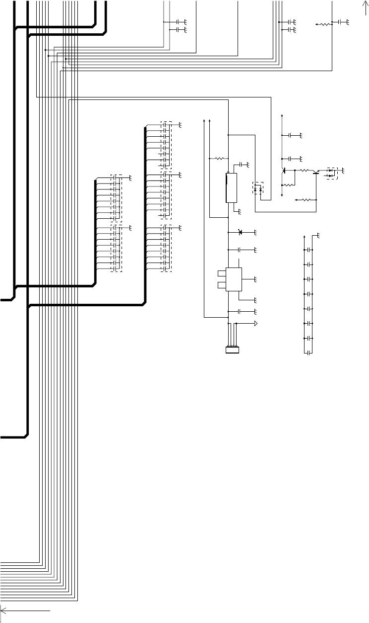
– 62 –
D
8D
9D
1
0
D
1
1
D
1
2
D
1
3
D
1
4
D
1
5
23498765
1
CA3
220P × 8
D
0D
1D
2D
3D
4D
5D
6D
7
23498765
1
CA4
220P × 8
A
2
0
A
1
7
A
1
5
A
1
3
A
1
1
A
9
23456789
1
CA2
220P × 8
A
1
9
A
1
8
A
1
6
A
1
4
A
1
2
A
1
0
A
8
23456789
1
CA1
220P × 8
A
0A
1A
2A
3A
4A
5A
6A
7
23456789
1
CA5
220P × 8
VCC
0.1U × 8
C10
(IC12)
C115
(IC4)
C124
(IC5)
C112
(IC7)
C132
(IC9)
C116
(IC6)
C138
(IC11)
C136
(IC10)
+ +
31
095
CN3
5273-04A
1
2
3
4
C1
1000U
35V 2
1
VI
RC
VO
VR
G
N
D
6
8
4
IC2
HLD051R2M
C6
1000U
35V ZD1
RD7.5EB1
1
3
5
4
VCC
GND
RESET
CD
IC4
M51953BL C2
0.47U
50V
DD3
DCB010
++
VCC
VCC R125
10K
Q6
A1338
R126
10K
R24
1K
C7
0.047
5.5V
C109
0.1U
Q7
C3875
DD2
DCB010
R121
1K
VP
VCC
VB
POWER BLOCK
BUS BLOCK
C133
33P C12
33P
C5
33P C3
33P
VB
R102
10K
C100
33P
D
SIDE C
B

– 63 –
C1 05041081 CHEM. CAPA. 1000UF 35V 1
C2 05054745 CHEM. CAPA. 0.47UF 50V 1
C3-5 05753304 CERA. CAPA. CHIP 33PF 50V 3
C6 05041081 CHEM. CAPA. 1000UF 35V 1
C7 05994732 BACK-UP CAPA. FYD0H473Z 1
C8-9 05753304 CERA. CAPA. CHIP 33PF 50V 2
C10-11 05751045 CERA. CAPA. CHIP 0.1UF 50V 2
C12 05753304 CERA. CAPA. CHIP 33PF 50V 1
C13-15 05751045 CERA. CAPA. CHIP 0.1UF 50V 3
C100-108 05753304 CERA. CAPA. CHIP 33PF 50V 9
C109-116 05751045 CERA. CAPA. CHIP 0.1UF 50V 8
C117 05753304 CERA. CAPA. CHIP 33PF 50V 1
C118 05751045 CERA. CAPA. CHIP 0.1UF 50V 1
C119 05753304 CERA. CAPA. CHIP 33PF 50V 1
C120-123 05751015 CERA. CAPA. CHIP 100PF 50V 4
C124-125 05751045 CERA. CAPA. CHIP 0.1UF 50V 2
C126 05753304 CERA. CAPA. CHIP 33PF 50V 1
C127 05751015 CERA. CAPA. CHIP 100PF 50V 1
C128-131 05753304 CERA. CAPA. CHIP 33PF 50V 4
C132 05751045 CERA. CAPA. CHIP 0.1UF 50V 1
C133 05753304 CERA. CAPA. CHIP 33PF 50V 1
C134-138 05751045 CERA. CAPA. CHIP 0.1UF 50V 5
CA1-5 05652212 CAPA. ARRAY 220PF 50V 8EL 5
R1 06753314 CHIP RESISTOR 330 OHM 1/10W 1
R2-3 06753324 CHIP RESISTOR 3.3 K-OHM 1/10W 2
R4-5 06753304 CHIP RESISTOR 33 OHM 1/10W 2
R6 06751031 CHIP RESISTOR 10 K-OHM 1/10W 1
R7-8 06753304 CHIP RESISTOR 33 OHM 1/10W 2
R9 06751031 CHIP RESISTOR 10 K-OHM 1/10W 1
R10 06753304 CHIP RESISTOR 33 OHM 1/10W 1
R11 06751021 CHIP RESISTOR 1 K-OHM 1/10W 1
R12-14 06753304 CHIP RESISTOR 33 OHM 1/10W 3
R15 06751031 CHIP RESISTOR 10 K-OHM 1/10W 1
R16 06021024 RD RESISTOR 1 K-OHM 1/2W 1
R17 06751031 CHIP RESISTOR 10 K-OHM 1/10W 1
R18 06753304 CHIP RESISTOR 33 OHM 1/10W 1
R19 06751031 CHIP RESISTOR 10 K-OHM 1/10W 1
R20-23 06753304 CHIP RESISTOR 33 OHM 1/10W 4
R24 06751021 CHIP RESISTOR 1 K-OHM 1/10W 1
R25 06751031 CHIP RESISTOR 10 K-OHM 1/10W 1
R26 06754721 CHIP RESISTOR 4.7 K-OHM 1/10W 1
R27 06751031 CHIP RESISTOR 10 K-OHM 1/10W 1
R28 06754721 CHIP RESISTOR 4.7 K-OHM 1/10W 1
R29 06751021 CHIP RESISTOR 1 K-OHM 1/10W 1
R30 06754721 CHIP RESISTOR 4.7 K-OHM 1/10W 1
R31 06752725 CHIP RESISTOR 2.7 K-OHM 1/10W 1
R32 06754721 CHIP RESISTOR 4.7 K-OHM 1/10W 1
R33 06752725 CHIP RESISTOR 2.7 K-OHM 1/10W 1
R100 06751031 CHIP RESISTOR 10 K-OHM 1/10W 1
R101 06752215 CHIP RESISTOR 220 OHM 1/10W 1
R102-103 06751031 CHIP RESISTOR 10 K-OHM 1/10W 2
R104-105 06753324 CHIP RESISTOR 3.3 K-OHM 1/10W 2
R106 06752031 CHIP RESISTOR 20 K-OHM 1/10W 1
R107-108 06751031 CHIP RESISTOR 10 K-OHM 1/10W 2
R109-110 06752031 CHIP RESISTOR 20 K-OHM 1/10W 2
R111 06751031 CHIP RESISTOR 10 K-OHM 1/10W 1
4-2. Parts List Main Logic Board
DRWG.NO. REV. PARTS NO. PARTS NAME Q'TY REMARKS RANK

– 64 –
R112-114 06752031 CHIP RESISTOR 20 K-OHM 1/10W 3
R115 06751031 CHIP RESISTOR 10 K-OHM 1/10W 1
R116 06754721 CHIP RESISTOR 4.7 K-OHM 1/10W 1
R117 06751031 CHIP RESISTOR 10 K-OHM 1/10W 1
R118 06753304 CHIP RESISTOR 33 OHM 1/10W 1
R119-120 06751031 CHIP RESISTOR 10 K-OHM 1/10W 2
R121 06751021 CHIP RESISTOR 1 K-OHM 1/10W 1
R122 06753324 CHIP RESISTOR 3.3 K-OHM 1/10W 1
R123 06753304 CHIP RESISTOR 33 OHM 1/10W 1
R124-126 06751031 CHIP RESISTOR 10 K-OHM 1/10W 3
R127 06751021 CHIP RESISTOR 1 K-OHM 1/10W 1
R128 06752031 CHIP RESISTOR 20 K-OHM 1/10W 1
R129-131 06754721 CHIP RESISTOR 4.7 K-OHM 1/10W 3
R132-133 06751021 CHIP RESISTOR 1 K-OHM 1/10W 2
R134 06754721 CHIP RESISTOR 4.7 K-OHM 1/10W 1
R135 06752215 CHIP RESISTOR 220 OHM 1/10W 1
R136-137 06751021 CHIP RESISTOR 1 K-OHM 1/10W 2
RA1 06581039 RESIS. ARRAY 10 K-OHM 1/8W 4EL 1
VR1 06454732 RP RESISTOR RH0615C-47K 1
VR2-4 06454721 RP RESISTOR RH0615CS-4.7K 3
Q1 07320101 TRANSISTOR 2SD2010 1 S
Q2-3 07113591 TRANSISTOR 2SB1359 2 S
Q4 07016491 TRANSISTOR 2SA1649 1
Q5-6 07013381 CHIP TRANSISTOR 2SA1338-67*TA 2 S
Q7 07238754 CHIP TRANSISTOR 2SC3875S-G*AL 1 S
Q8-9 07320101 TRANSISTOR 2SD2010 2
DQ1-3 07603016 DIGITAL TRANSISTOR FA1A4P 3 S
DQ4 07603017 DIGITAL TRANSISTOR FN1A4P 1
DQ5-6 07603016 DIGITAL TRANSISTOR FA1A4P 2
DQ7-9 07603017 DIGITAL TRANSISTOR FN1A4P 3
TA1 07650054 TRANSISTOR ARRAY MP4020 1 S
D1 08000048 DIODE EG01YV0 1
D2-4 08000044 DIODE 1SR139-100AT 3
DD1-3 08000047 DIODE CHIP DCB010 3
ZD1 08020090 ZENER DIODE RD7.5EB1T 1
ZD2 08020095 ZENER DIODE RD4.7JSB1 1
IC1 08221043 SRAM 6264FP-100NS*EL 1
IC2 08202020 IC-REG HLD051R2M 1 S
IC3 08202011 IC-REG UPC7824 1 S
IC4 08200109 IC-RESET M51953BL 1 S
IC5 08251006 CPU HD6413003F10T 1 S
IC6-7 08221042 PSRAM 5P8128N-80L*E1 2
IC8 08222047 EEPROM KM93C46 1
09110115 IC SOCKET DILB-8P-8J 1
IC9 09110076 IC SOCKET DILB-42P-8J 1
IC10 08240076 GATE ARRAY D65622GF-TSP 1 S
IC11 08222091 EPROM M5M27C202K-12 1 TS4.**
09110020 IC SOCKET DICF-40C-JAE 1
IC12 08201022 IC-LIN HA17339F*TL 1
CN1 09100370 CONNECTOR 53014-0710 1
CN2 09100270 CONNECTOR 5483-02A 1
CN3 09100614 CONNECTOR 5273-04A 1
CN4 09100267 CONNECTOR 5483-06A 1
CN5 09100532 CONNECTOR 5483-04AX-RED 1
CN6 09100177 CONNECTOR 5332-26SG1 1
CN7 09100444 CONNECTOR 53014-1210 1
Main Logic Board
DRWG.NO. REV. PARTS NO. PARTS NAME Q'TY REMARKS RANK

– 65 –
Main Logic Board
CN8 09100516 CONNECTOR 53014-0510 1
CN9 09100610 CONNECTOR PHEC40R-R111 1
X1 09250037 CERA. OSCILLATOR CST9.83MT 1
FL1-5 09251119 LINE FILTER TU02MT*R 5
BZ1 45060201 BUZZER QMB-111P 1
DRWG.NO. REV. PARTS NO. PARTS NAME Q'TY REMARKS RANK
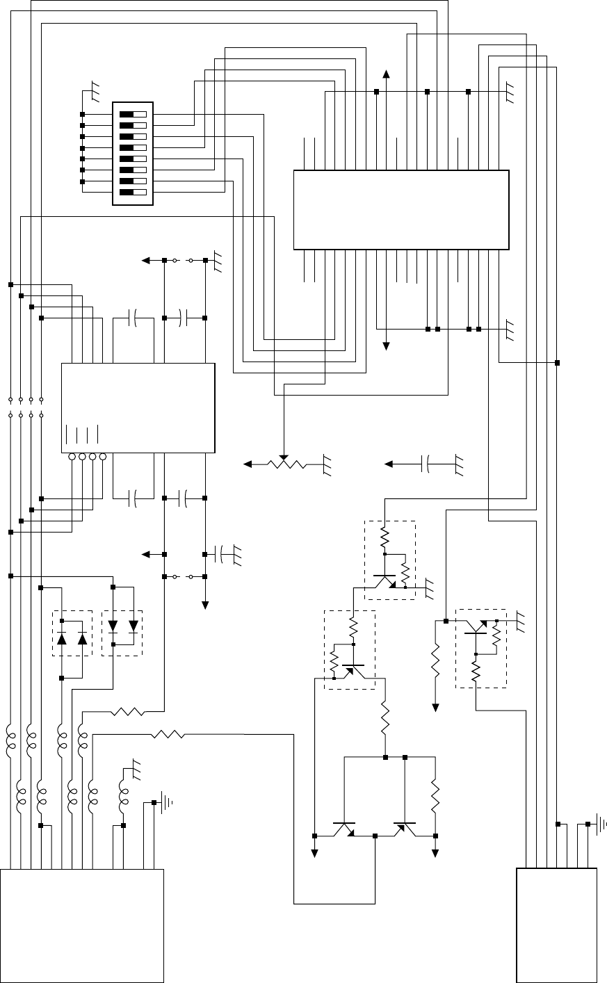
– 66 –
CN3
TXD
RXD
CTS
DTR
RCH
MP-DTR
MP-TXD
RTS
FAULT
GND
GND
F-GND
MOUNT-HOLE
2
3
5
20
11
16
15
4
14
7
13
1
0
L5
L8
L4
L1
L9
DBLD-J255AF-21L91
B-01R × 9L3
L7
L6
L2
R2
3.3K
D2
D1
R4
3.3K DCB010
× 2
+ +
+
+
JP6
VCC
C4
0.1U
V+ C2
1U
50V
C6
1U
50V
3
2
16
14
13
8
7
1
11
12
9
10
4
5
6
15
D1O
R1I
R2I
D2O
C1+
D1I
R1O
R2O
D2I
C2+
C1–
V+ C2–
V–
IC1
GND
HD151232FP
C1
1U
50V
C5
1U
50V
V–
JP5
JP4
JP3
JP2
JP1
V+
TR2
C3875
TR4
A1179
R5
33K
VCC
R3
1K
TR3
FN1A4P
R1
10K
TR5
FA1A4P
TR1
FA1A4P
CN2
PSW
PEXT 1
PEXT 2
VEXT
VEXT
F-GND
MOUNT-HOLE
52065-6645
6
2
5
3
4
1
0
CN1
A1
A2
A3
A4
A5
A6
A7
A8
A9
A10
A11
A12
A13
A14
A15
A16
A17
A18
A19
A20
B1
B2
B3
B4
B5
B6
B7
B8
B9
B10
B11
B12
B13
B14
B15
B16
B17
B18
B19
B20
VVR
DIN1
DIN3
DIN5
DIN7
GND
VCC
/DIEN
GND
RXD
ID0
ID2
GND
PEXT 1
VEXT
VCC
GND
DIN2
DIN4
DIN6
DIN8
GND
VCC
/FAULT
DTR
GND
TXD
CTS
ID1
GND
PSWIN
PEXT 2
VEXT
VCC
PHEC40P-R111
DSW1
87654321
91
01
11
21
31
41
51
6
1
VCC
2
C3
220U
6.3V
+
VR1
EVN-D2A-10K
V–
VCC
VCC
3
1
5. RS232C Interface Board
5-1. Circuit Diagram

– 67 –
5-2. Parts List RS232C Interface Board
DRWG.NO. REV. PARTS NO. PARTS NAME Q'TY REMARKS RANK
C1-2 05051057 CHEM. CAPA. 1UF 50V 2
C3 05002213 CHEM. CAPA. 220UF 6.3V 1
C4 05751045 CERA. CAPA. CHIP 0.1UF 50V 1
C5-6 05051057 CHEM. CAPA. 1UF 50V 2
R1 06751031 CHIP RESISTOR 10 K-OHM 1/10W 1
R2 06753324 CHIP RESISTOR 3.3 K-OHM 1/10W 1
R3 06751021 CHIP RESISTOR 1 K-OHM 1/10W 1
R4 06753324 CHIP RESISTOR 3.3 K-OHM 1/10W 1
R5 06753334 CHIP RESISTOR 33 K-OHM 1/10W 1
VR1 06451033 RP RESISTOR EVN-D2A-10K 1
TR1 07603016 DIGITAL TRANSISTOR FA1A4P 1
TR2 07238754 CHIP TRANSISTOR 2SC3875S-G*AL 1
TR3 07603017 DIGITAL TRANSISTOR FN1A4P 1
TR4 07011793 CHIP TRANSISTOR 2SA1179M6-STR 1
TR5 07603016 DIGITAL TRANSISTOR FA1A4P 1
D1-2 08000047 DIODE CHIP DCB010 2
IC1 08200155 IC-I/F HD151232FP*TL 1
DSW1 *2 09090034 DIP SWITCH KSS08-1 1
#2 09090046 DIP SWITCH EAH108L-BLK 1
CN1 09100611 CONNECTOR PHEC40P-R111 1
CN2 09100421 CONNECTOR 52065-6645 1
CN3 09100483 CONNECTOR DBLD-J25SAF-21L9-1 1
L1-9 09990705 BEADS INDUCTOR B01-RT 9
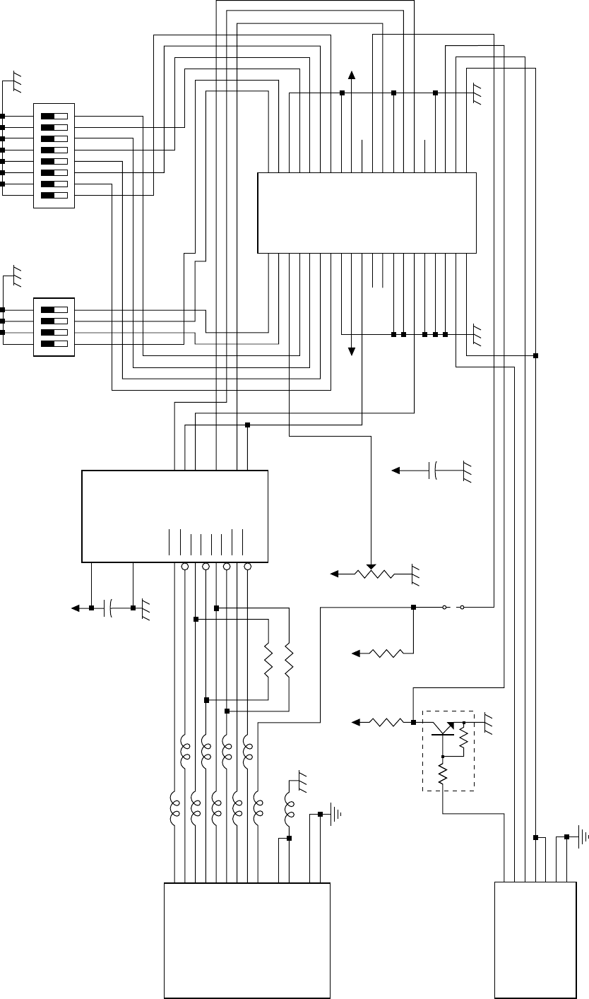
– 68 –
CN3
SD (+)
SD (–)
RD (+)
RD (–)
CS (+)
CS (–)
RS (+)
RS (–)
FAULT
GND
GND
F-GND
MOUNT-HOLE
9
10
17
18
19
23
24
25
14
7
13
1
0
L4
L1
L2
L6
DBLD-J255AF-21L9
L3
L8
L9
L5
L10
L7
JP1
CN2
PSW
PEXT 1
PEXT 2
VEXT
VEXT
F-GND
MOUNT-HOLE
52065-6645
6
2
5
3
4
1
0
CN1
A1
A2
A3
A4
A5
A6
A7
A8
A9
A10
A11
A12
A13
A14
A15
A16
A17
A18
A19
A20
B1
B2
B3
B4
B5
B6
B7
B8
B9
B10
B11
B12
B13
B14
B15
B16
B17
B18
B19
B20
DIN9
DIN11
VVR
DIN1
DIN3
DIN5
DIN7
GND
VCC
DOEN
/DIEN
GND
RD
ID0
ID2
GND
PEXT 1
VEXT
VCC
DIN10
DIN12
GND
DIN2
DIN4
DIN6
DIN8
GND
VCC
FAULT
RS
GND
SD
CS
ID1
GND
PSWIN
PEXT 2
VEXT
VCC
PHEC40P-R111
DSW1
87654321
91
01
11
21
31
41
51
6
1
VCC
2
C2
220U
6.3V
+
VR1
EVN-D2A-10K
VCC
3
1
VCC VCC
R3
10K R4
10K
TR1
FA1A4P
1
DSW2
4321
5678
MC34051M
VCC
16
8
14
13
6
7
2
1
10
11
15
4
5
3
9
12
C1
0.1U
IC1
VCC
GND
D1O+
D1O–
R2I+
R2I–
R1I+
R1I–
D2O+
D2O–
D1I
D1EN
R1O
R2O
D2I
D2EN
R1
R2
B-01R × 10
100 × 2
6. RS422A Interface Board
6-1. Circuit Diagram

– 69 –
6-2. Parts List RS422A Interface Board
DRWG.NO. REV. PARTS NO. PARTS NAME Q'TY REMARKS RANK
C1 05751045 CERA. CAPA. CHIP 0.1UF 50V 1
C2 05002213 CHEM. CAPA. 220UF 6.3V 1
R1-2 06751014 CHIP RESISTOR 100 OHM 1/10W 2
R3-4 06751031 CHIP RESISTOR 10 K-OHM 1/10W 2
VR1 06451033 RP RESISTOR EVN-D2A-10K 1
TR1 07603016 DIGITAL TRANSISTOR FA1A4P 1
IC1 08200127 IC-I/F MC34051M 1
DSW1 *2 09090034 DIP SWITCH KSS08-1 1
#2 09090046 DIP SWITCH EAH108L-BLK 1
DSW2 *2 09090033 DIP SWITCH KSS04-1 1
#2 09090045 DIP SWITCH EAH104L-BLK 1
CN1 09100611 CONNECTOR PHEC40P-R111 1
CN2 09100421 CONNECTOR 52065-6645 1
CN3 09100483 CONNECTOR DBLD-J25SAF-21L9-1 1
L1-10 09990705 BEADS INDUCTOR B01-RT 10
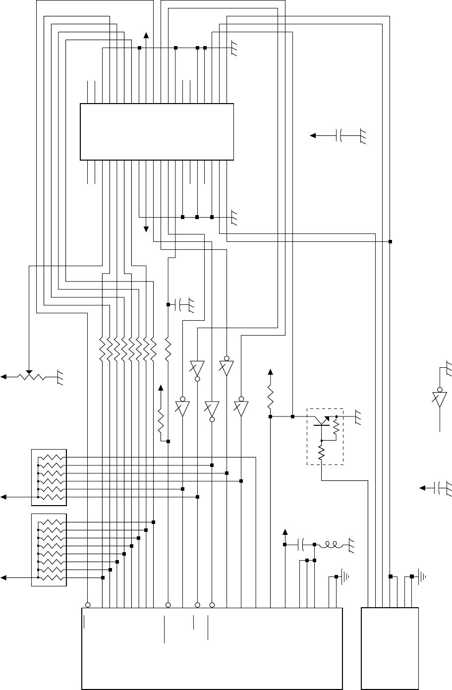
– 70 –
CN3
INIT
DATA1
DATA2
DATA3
DATA4
DATA5
DATA6
DATA7
DATA8
STROBE
BUSY
ACK
ERROR
SLCT
PE
SLCT-IN
CPL
VCC
GND
EXT-GND
RETURN-GND
F-GND
MOUNT-HOLE
57RE-40360-BD29
VR1
EVN-D2A-10K
TR1
FA1A4P
CN2
PSW
PEXT 1
PEXT 2
VEXT
VEXT
F-GND
MOUNT-HOLE
52065-6645
6
2
5
3
4
1
0
CN1
A1
A2
A3
A4
A5
A6
A7
A8
A9
A10
A11
A12
A13
A14
A15
A16
A17
A18
A19
A20
B1
B2
B3
B4
B5
B6
B7
B8
B9
B10
B11
B12
B13
B14
B15
B16
B17
B18
B19
B20
VVR
DIN1
DIN3
DIN5
DIN7
GND
VCC
ERROR
/SLCT
/BUSY
STB
GND
ID0
ID2
GND
PEXT 1
VEXT
VCC
GND
DIN2
DIN4
DIN6
DIN8
GND
VCC
/INIT
/PE
ACK
GND
ID1
GND
PSWIN
PEXT 2
VEXT
VCC
PHEC40P-R111
2
VCC
C2
220U
6.3V
+
VCC
3
1
C3
1000P
R2
R3
R4
R5
R6
R7
R8
R9
R1
1K VCC
VCC
1RA2
1.8K × 6
234567
VCC
1RA1
4.7K × 8
45678923
–30
VCC
L1
B-01R
C1
0.1U
31
2
3
4
5
6
7
8
9
1
11
10
32
13
12
36
34
18
16
33
19
17
0
VCC
R10
10K
4.7K × 8
R11
100
C
D
B
F
E
65
12 13
89
43
10 11
IC1
LS05
VCC
C4
0.1U
(IC1)
AIC1
21
LS05
7. Centronics Interface Board
7-1. Circuit Diagram

– 71 –
7-2. Parts List Centronics Interface Board
DRWG.NO. REV. PARTS NO. PARTS NAME Q'TY REMARKS RANK
C1 05751045 CERA. CAPA. CHIP 0.1UF 50V 1
C2 05002213 CHEM. CAPA. 220UF 6.3V 1
C3 05751025 CERA. CAPA. CHIP 1000PF 50V 1
C4 05751045 CERA. CAPA. CHIP 0.1UF 50V 1
R1 06751021 CHIP RESISTOR 1 K-OHM 1/10W 1
R2-9 06754721 CHIP RESISTOR 4.7 K-OHM 1/10W 8
R10 06751031 CHIP RESISTOR 10 K-OHM 1/10W 1
R11 06751014 CHIP RESISTOR 100 OHM 1/10W 1
RA1 06584729 RESIS. ARRAY 4.7K-OHM 1/8W 8EL 1
RA2 06581824 RESIS. ARRAY 1.8K-OHM 1/8W 6EL 1
VR1 06451033 RP RESISTOR EVN-D2A-10K 1
TR1 07603016 DIGITAL TRANSISTOR FA1A4P 1
IC1 08210142 TTL IC 74LS05FP*TL 1
CN1 09100611 CONNECTOR PHEC40P-R111 1
CN2 09100421 CONNECTOR 52065-6645 1
CN3 09100482 CONNECTOR 57RE40360-730BD29 1
L1 09990705 BEADS INDUCTOR B01-RT 1
– 72 –
8. Control Panel Board
8-1. Circuit Diagram
CN1
53014-1210
2
3
4
1
8
9
10
11
12
7
6
5
SW-CO
SW-FEED
SW-ONL
GND
LED-POW
LED-ONL
LED-PAR
LED-HUP
LED-ERR
+5V
PSW
PSW-2
PSW-1
SW2
SW1
R1
270
LED1
LT-1E21A
R5
270
LED5
LT-1E21A
R3
270
LED3
LT-1D11A
R2
270
LED2
LT-1D11A
R4
270
JP2 D2
1S1588
JP1 D1
1S1588
LED4
LT-1D11A

– 73 –
R1-5 06052714 RD RESISTOR 270 OHM 1/6W 5
D1-2 08000039 DIODE 1S1588 2
LED1 08300058 LED LT-1E21A 1
LED2-4 08300081 LED LT-1D11A 3
LED5 08300058 LED LT-1E21A 1
SW1-2 *1 09010043 PUSH SWITCH SKHHAL=S 2
#1 09010041 PUSH SWITCH SKHHAL 2
CN1 09100444 CONNECTOR 53014-1210 1
CN2 NOT MOUNTED
- 09090047 LEAF SWITCH MSW-1705C 1
80700580 WIRE 26UL1571ORG050 2
Control Panel Board
8-2. Parts List
DRWG.NO. REV. PARTS NO. PARTS NAME Q'TY REMARKS RANK
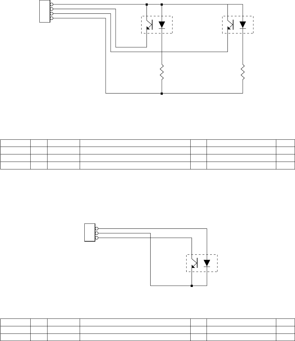
– 74 –
9. Paper-Out Detector Board
9-1. Circuit Diagram
9-2. Parts List Paper-Out Detector
10. Label Sensor Board
10-1.Circuit Diagram
10-2.Parts List Transmissive Sensor
DRWG.NO. REV. PARTS NO. PARTS NAME Q'TY REMARKS RANK
R1-2 06052211 RD RESISTOR 220 OHM 1/6W 2
PS1-2 08300082 PHOTO-INTERRUPTER PS6002A-KS 2
- 30721010 CABLE UNIT TMP4 1
DRWG.NO. REV. PARTS NO. PARTS NAME Q'TY REMARKS RANK
PS1 08300150 PHOTO-INTERRUPTER TLP833 1
CN1 09100460 CONNECTOR 53014-0310 1
3
2
1
CN1
LED
GND
LABEL
53014-0310
PS1
TLP833
(LABEL)
4
3
2
1
CN1
VCC
MARK
PE
GND
(51015-0400)
PS1
PS60002
(MARK)
PS2
PS60002
(PE)
R1
220 R2
220
P1994.12
P1995.06

Printed in Japan, 80822421-B
Distributed by
STAR MICRONICS DEUTSCHLAND GMBH
Westerbachstraße 59,
D-60489 Frankfurt, Germany
Telefon: 069 78 99 90
Telefax: 069 78 10 06
Telex: 4 175825 star d
STAR MICRONICS U.K. LTD.
Star House, Peregrine Business
Park, Gomm Road, High Wycombe
Bucks, HP13 7DL U.K.
Tel: 01494-471111
Fax: 01494 473333
Telex: 83393 STAR UK
HEAD OFFICE
STAR MICRONICS CO., LTD.
536 Nanatsushinnya, Shimizu,
Shizuoka, 424, Japan
Tel: 0543-47-0112
Fax: 0543-48-5271
OVERSEAS SUBSIDIARY COMPANIES
STAR MICRONICS AMERICA, INC.
70-D Ethel Road West,
Piscataway, NJ 08854, U.S.A.
Tel: (908)572-9512
Telefax: (908)572-5095
