Sylvania LC200SL8 User Manual LCD TELEVISION Manuals And Guides L0705170
SYLVANIA LCD Television Manual L0705170 SYLVANIA LCD Television Owner's Manual, SYLVANIA LCD Television installation guides
User Manual: Sylvania LC200SL8 LC200SL8 SYLVANIA LCD TELEVISION - Manuals and Guides View the owners manual for your SYLVANIA LCD TELEVISION #LC200SL8. Home:Electronics Parts:Sylvania Parts:Sylvania LCD TELEVISION Manual
Open the PDF directly: View PDF ![]() .
.
Page Count: 57
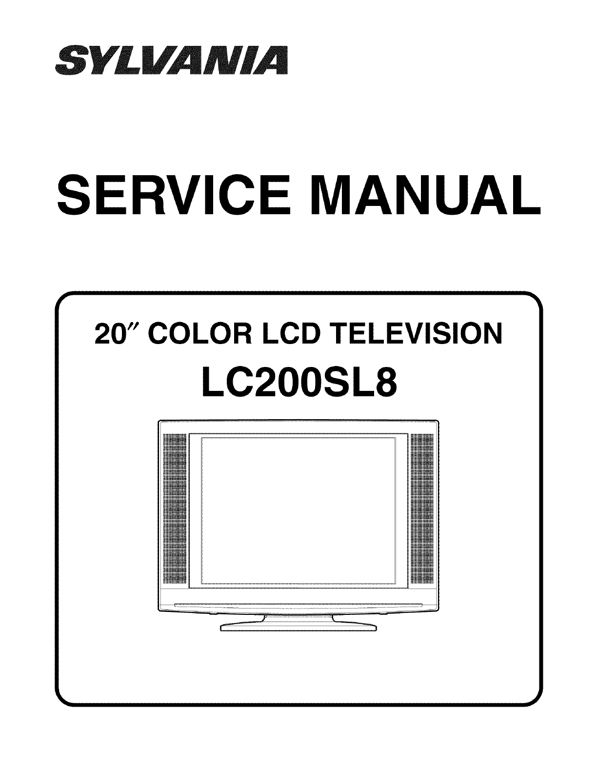
SY#..VA/I/#A
SERVICE MANUAL
20" COLOR LCD TELEVISION
LC200SL8
iiiiWiiiiiii
ii£i_iiiiEii
iiiiJ|iii
iiiiiiiiiiiiiiii
iii£_ii£_ii£i
iiiiimiim£i
iii£EiEii
iii£_ii£iim
ii£iEiEii
iiiiiii|iii
iiiiiiiiiiiiiiii
iii£_ii£_ii£i
iii£_ii£_ii£i
iiiiiEiEii
iii£EiEii
iiiii_iiiiiiiiii
iiiiiiiiiiii
iiiiiiiiii
iiiiii|ii
_iiii_iiiiiiiii
iiiiiiii|ii
iiiiiiiiiiiiiii
_iiii_iiii_iiii
_iiii_iiii_iiii
_iiii_iiii_iiii
_iiii_iiiiiiiii
_iiii_iiiiiiiii
iiiiiiii|ii
iiiiiiiiiiiiiii
_iiii_iiii_iiii
_iiii_iiii_iiii
_iiii_iiii_iiii
_iiii_iiiiiiiii
_iiii_iiiiiiiii
iiiiiiii|ii
iiiiiiiii
..... J
IMPORTANT SAFETY NOTICE
Proper service and repair is important to the safe, reliable operation of all
Funai Equipment. The service procedures recommended by Funai and
described in this service manual are effective methods of performing
service operations. Some of these service special tools should be used
when and as recommended.
It is important to note that this service manual contains various CAUTIONS
and NOTICES which should be carefully read in order to minimize the risk
of personal injury to service personnel. The possibility exists that improper
service methods may damage the equipment. It also is important to
understand that these CAUTIONS and NOTICES ARE NOT EXHAUSTIVE.
Funai could not possibly know, evaluate and advice the service trade of all
conceivable ways in which service might be done or of the possible
hazardous consequences of each way. Consequently, Funai has not
undertaken any such broad evaluation. Accordingly, a servicer who uses a
service procedure or tool which is not recommended by Funai must first
use all precautions thoroughly so that neither his safety nor the safe
operation of the equipment will be jeopardized by the service method
selected.
TABLE OF CONTENTS
Specifications ........................................................................... 1-1
Important Safety Precautions ............................................................... 2-1
Standard Notes for Servicing ............................................................... 3-1
Cabinet Disassembly Instructions ............................................................ 4-1
Electrical Adjustment Instructions ............................................................ 5-1
How to initialize the LCD Television .......................................................... 6-1
Block Diagrams .......................................................................... 7-1
Schematic Diagrams /CBA's and Test Points ................................................... 8-1
Waveforms ............................................................................. 9-1
Wiring Diagram ......................................................................... 10-1
IC Pin Function Descriptions ............................................................... 11-1
Exploded Views ......................................................................... 12-1
Mechanical Parts List .................................................................... 13-1
Electrical Parts List ...................................................................... 14-1
The LCD panel is manufactured to provide many years of useful life.
Occasionally a few non active pixels may appear as a tiny spec of color.
This is not to be considered a defect in the LCD screen.
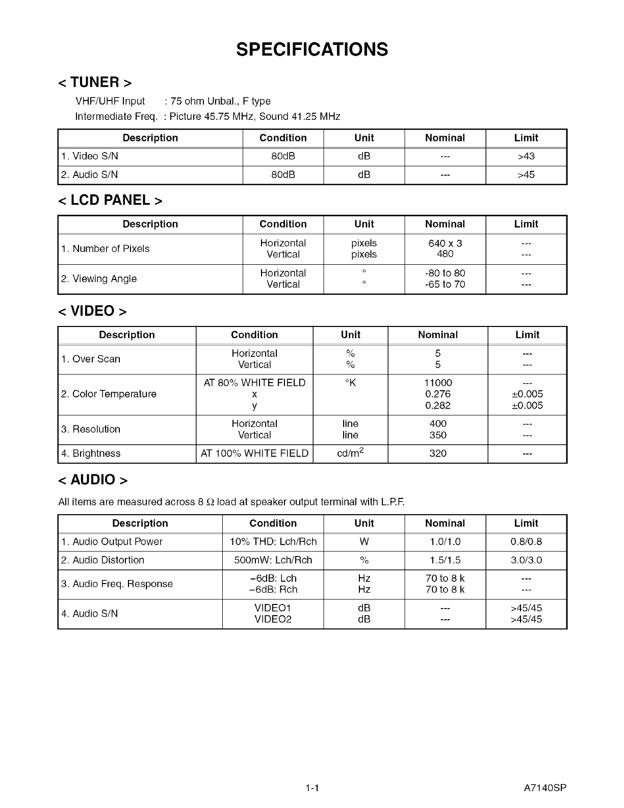
SPECIFICATIONS
<TUNER >
VHF/UHF Input : 75 ohm Unbal, F type
Intermediate Freq. : Picture 45.75 MHz, Sound 41.25 MHz
Description Condition
1. Video S/N 80dB
2. Audio S/N 80dB
Unit Nominal Limit
dB --- >43
dB --- >45
< LCD PANEL >
Description Condition Unit Nominal Limit
Horizontal pixels 640 x 3 ---
1. Number of Pixels Vertical pixels 480 ---
Horizontal ° -80 to 80 ---
2. Viewing Angle Vertical ° -65 to 70 ---
< VIDEO >
Description Condition Unit Nominal Limit
Horizontal % 5 ---
1. Over Scan Vertical % 5 ---
AT 80% WHITE FIELD °K 11000 ---
2. Color Temperature x 0.276 _+0.005
y 0.282 +0.005
Horizontal line 400 ---
3. Resolution Vertical line 350 ---
4. Brightness AT 100% WHITE FIELD cd/m 2 320 ---
< AUDIO >
All items are measured across 8 _ load at speaker output terminal with L.P.E
Description Condition Unit Nominal Limit
1. Audio Output Power 10% THD: Lch/Rch W 1.0/1.0 0.8/0.8
2. Audio Distortion 500mW: Lch/Rch % 1.5/1.5 3.0/3.0
-6dB: Lch Hz 70 to 8 k ---
3. Audio Freq. Response -6dB: Rch Hz 70 to 8 k ---
VIDEO1 dB --- >45/45
4. Audio S/N VIDEO2 dB --- >45/45
1-1 A7140SP
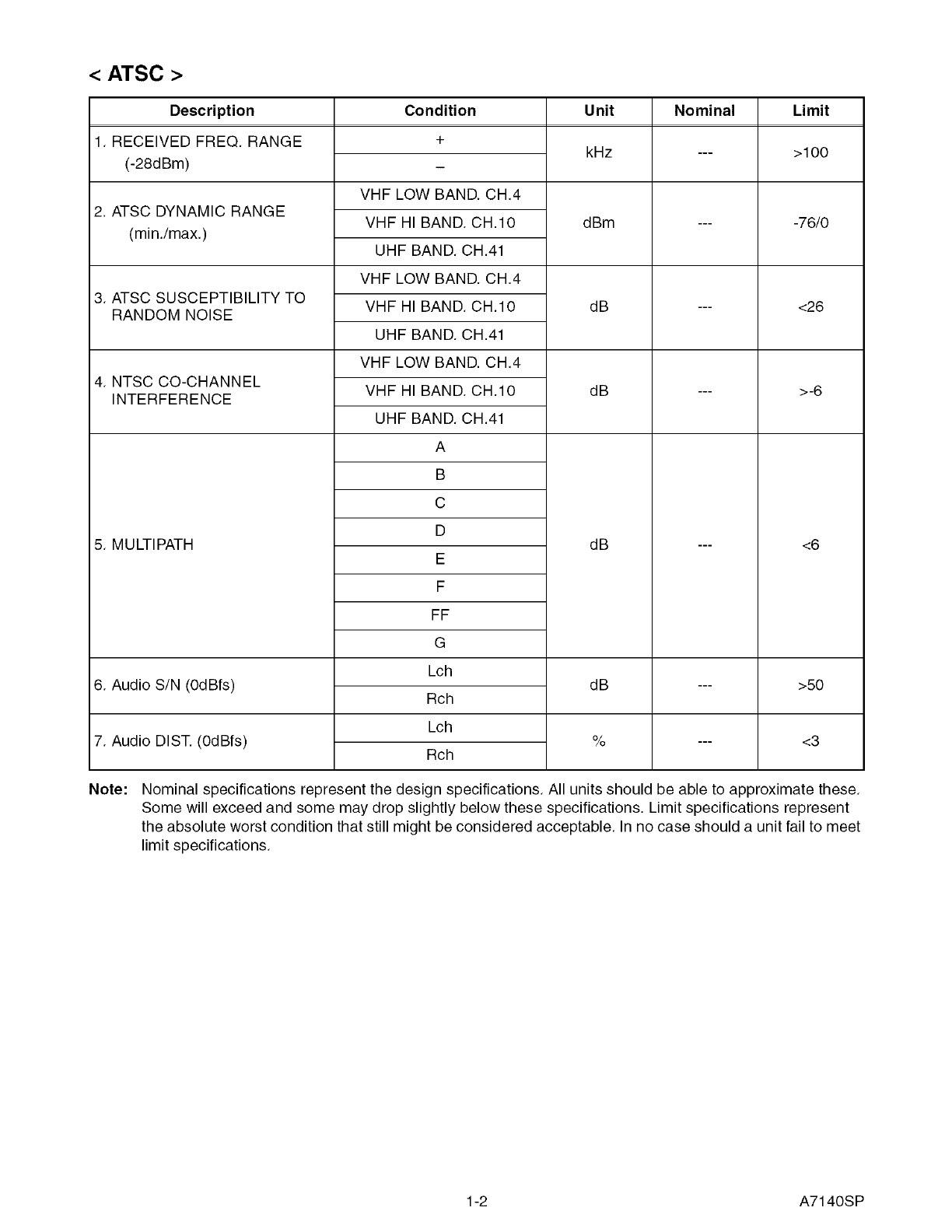
<ATSC >
Description
1. RECEIVED FREQ. RANGE
(-28dBm)
2. ATSC DYNAMIC RANGE
(min./max.)
3. ATSC SUSCEPTIBILITY TO
RANDOM NOISE
4. NTSC CO-CHANNEL
INTERFERENCE
5. MULTI PATH
6. Audio S/N (0dBfs)
7. Audio DIST. (0dBfs)
Condition
+
VHF LOW BAND. CH.4
VHF HI BAND. CH.10
UHF BAND. CH.41
VHF LOW BAND. CH.4
VHF HI BAND. CH.10
UHF BAND. CH.41
VHF LOW BAND. CH.4
VHF HI BAND. CH.10
UHF BAND. CH.41
A
B
C
D
E
F
FF
G
Lch
Rch
Lch
Rch
Unit
kHz
dBm
dB
dB
dB
dB
%
Nominal Limit
>100
-76/0
<26
>-6
<6
>5O
<3
Note: Nominal specifications represent the design specifications. All units should be able to approximate these.
Some will exceed and some may drop slightly below these specifications. Limit specifications represent
the absolute worst condition that still might be considered acceptable. In no case should a unit fail to meet
limit specifications.
1-2 A7140SP
IMPORTANT SAFETY PRECAUTIONS
Prior to shipment from the factory, our products are strictly inspected for recognized product safety and electrical
codes of the countries in which they are to be sold. However, in order to maintain such compliance, it is equally
important to implement the following precautions when a set is being serviced.
Safety Precautions for LCD TV
Circuit
Before returning an instrument to the
customer, always make a safety check of the
entire instrument, including, but not limited to, the
following items:
a. Be sure that no built-in protective devices are
defective and have been defeated during
servicing. (1) Protective shields are provided
on this chassis to protect both the technician
and the customer. Correctly replace all missing
protective shields, including any removed for
servicing convenience. (2) When reinstalling
the chassis and/or other assembly in the
cabinet, be sure to put back in place all
protective devices, including but not limited to,
nonmetallic control knobs, insulating
fishpapers, adjustment and compartment
covers/shields, and isolation resistor/capacitor
networks. Do not operate this instrument or
permit it to be operated without all
protective devices correctly installed and
functioning. Servicers who defeat safety
features or fail to perform safety checks
may be liable for any resulting damage.
b. Be sure that there are no cabinet openings
through which an adult or child might be able to
insert their fingers and contact a hazardous
voltage. Such openings include, but are not
limited to, (1) spacing between the Liquid
Crystal Panel and the cabinet mask, (2)
excessively wide cabinet ventilation slots, and
(3) an improperly fitted and/or incorrectly
secured cabinet back cover.
c. Antenna Cold Check - With the instrument AC
plug removed from any AC source, connect an
electrical jumper across the two AC plug
prongs. Place the instrument AC switch in the
on position. Connect one lead of an ohmmeter
to the AC plug prongs tied together and touch
the other ohmmeter lead in turn to each tuner
antenna input exposed terminal screw and, if
applicable, to the coaxial connector. If the
measured resistance is less than 1.0 megohm
or greater than 5.2 megohm, an abnormality
exists that must be corrected before the
instrument is returned to the customer. Repeat
this test with the instrument AC switch in the oft
position.
.
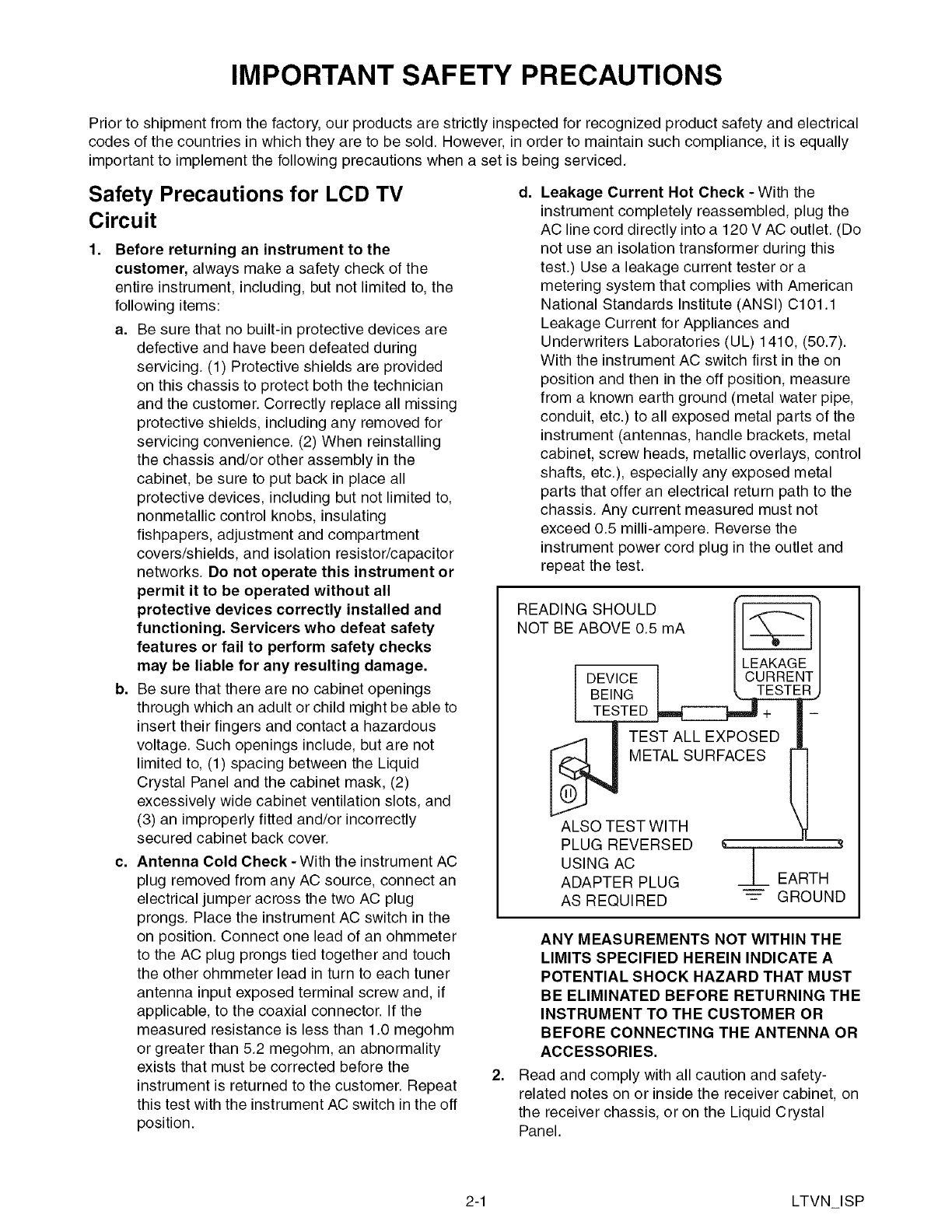
d. Leakage Current Hot Check - With the
instrument completely reassembled, plug the
AC line cord directly into a 120 V AC outlet. (Do
not use an isolation transformer during this
test.) Use a leakage current tester or a
metering system that complies with American
National Standards Institute (ANSI) C101.1
Leakage Current for Appliances and
Underwriters Laboratories (UL) 1410, (50.7).
With the instrument AC switch first in the on
position and then in the off position, measure
from a known earth ground (metal water pipe,
conduit, etc.) to all exposed metal parts of the
instrument (antennas, handle brackets, metal
cabinet, screw heads, metallic overlays, control
shafts, etc.), especially any exposed metal
parts that offer an electrical return path to the
chassis. Any current measured must not
exceed 0.5 milli-ampere. Reverse the
instrument power cord plug in the outlet and
repeat the test.
READING SHOULD
NOT BE ABOVE 0.5 mA
r"-
DEVICE [I_T
BEING - .
TESTED l
TEST ALL EXPOSED
METAL SURFACES
ALSO TEST WITH
PLUG REVERSED _,
USING AC __L
ADAPTER PLUG EARTH
AS REQUIRED _ GROUND
ANY MEASUREMENTS NOT WITHIN THE
LIMITS SPECIFIED HEREIN INDICATE A
POTENTIAL SHOCK HAZARD THAT MUST
BE ELIMINATED BEFORE RETURNING THE
INSTRUMENT TO THE CUSTOMER OR
BEFORE CONNECTING THE ANTENNA OR
ACCESSORIES.
Read and comply with all caution and safety-
related notes on or inside the receiver cabinet, on
the receiver chassis, or on the Liquid Crystal
Panel.
2-1 LTVN ISP
3. Design Alteration Warning - Do not alter or add
to the mechanical or electrical design of this TV
receiver. Design alterations and additions,
including, but not limited to circuit modifications
and the addition of items such as auxiliary audio
and/or video output connections, might alter the
safety characteristics of this receiver and create a
hazard to the user. Any design alterations or
additions will void the manufacturer's warranty and
may make you, the servicer, responsible for
personal injury or property damage resulting
therefrom.
4. Hot Chassis Warning-
a. Some TV receiver chassis are electrically
connected directly to one conductor of the AC
power cord and maybe safety-serviced without
an isolation transformer only if the AC power
plug is inserted so that the chassis is
connected to the ground side of the AC power
source. To confirm that the AC power plug is
inserted correctly, with an AC voltmeter,
measure between the chassis and a known
earth ground. If a voltage reading in excess of
1.0V is obtained, remove and reinsert the AC
power plug in the opposite polarity and again
measure the voltage potential between the
chassis and a known earth ground.
b. Some TV receiver chassis normally have 85V
AC(RMS) between chassis and earth ground
regardless of the AC plug polarity. This chassis
can be safety-serviced only with an isolation
transformer inserted in the power line between
the receiver and the AC power source, for both
personnel and test equipment protection.
c. Some TV receiver chassis have a secondary
ground system in addition to the main chassis
ground. This secondary ground system is not
isolated from the AC power line. The two
ground systems are electrically separated by
insulation material that must not be defeated or
altered.
5. Observe original lead dress. Take extra care to
assure correct lead dress in the following areas: a.
near sharp edges, b. near thermally hot parts-be
sure that leads and components do not touch
thermally hot parts, c. the AC supply, d. high
voltage, and, e. antenna wiring. Always inspect in
all areas for pinched, out of place, or frayed wiring.
Check AC power cord for damage.
6. Components, parts, and/or wiring that appear to
have overheated or are otherwise damaged
should be replaced with components, parts, or
wiring that meet original specifications.
Additionally, determine the cause of overheating
and/or damage and, if necessary, take corrective
action to remove any potential safety hazard.
.Product Safety Notice - Some electrical and
mechanical parts have special safety-related
characteristics which are often not evident from
visual inspection, nor can the protection they give
necessarily be obtained by replacing them with
components rated for higher voltage, wattage, etc.
Parts that have special safety characteristics are
identified by a _ on schematics and in parts lists.
Use of a substitute replacement that does not
have the same safety characteristics as the
recommended replacement part might create
shock, fire, and/or other hazards. The product's
safety is under review continuously and new
instructions are issued whenever appropriate.
Prior to shipment from the factory, our products
are strictly inspected to confirm they comply with
the recognized product safety and electrical codes
of the countries in which they are to be sold.
However, in order to maintain such compliance, it
is equally important to implement the following
precautions when a set is being serviced.
2-2 LTVN_ISP
Precautions during Servicing
A. Parts identified by the _ symbol are critical for
safety.
Replace only with part number specified.
B. In addition to safety, other parts and assemblies
are specified for conformance with regulations
applying to spurious radiation. These must also be
replaced only with specified replacements.
Examples: RF converters, RF cables, noise
blocking capacitors, and noise blocking filters, etc.
C. Use specified internal wiring. Note especially:
1) Wires covered with PVC tubing
2) Double insulated wires
3) High voltage leads
D. Use specified insulating materials for hazardous
live parts. Note especially:
1) Insulation Tape
2) PVC tubing
3) Spacers
4) Insulators for transistors.
E. When replacing AC primary side components
(transformers, power cord, etc.), wrap ends of
wires securely about the terminals before
soldering.
F. Observe that the wires do not contact heat
producing parts (heat sinks, oxide metal film
resistors, fusible resistors, etc.)
G. Check that replaced wires do not contact sharp
edged or pointed parts.
H. When a power cord has been replaced, check that
5-6 kg of force in any direction will not loosen it.
I. Also check areas surrounding repaired locations.
J. Use care that foreign objects (screws, solder
droplets, etc.) do not remain inside the set.
K. Crimp type wire connector
The power transformer uses crimp type
connectors which connect the power cord and the
primary side of the transformer. When replacing
the transformer, follow these steps carefully and
precisely to prevent shock hazards.
Replacement procedure
1) Remove the old connector by cutting the wires
at a point close to the connector.
Important: Do not re-use a connector (discard
it).
2) Strip about 15 mm of the insulation from the
ends of the wires. If the wires are stranded,
twist the strands to avoid frayed conductors.
3) Align the lengths of the wires to be connected.
Insert the wires fully into the connector.
4) Use the crimping tool to crimp the metal sleeve
at the center position. Be sure to crimp fully to
the complete closure of the tool.
L. When connecting or disconnecting the internal
connectors, first, disconnect the AC plug from the
AC supply outlet.
M. When installing parts or assembling the cabinet
parts, be sure to use the proper screws and
tighten certainly.
2-3 LTVN ISP
Safety Check after Servicing
Examine the area surrounding the repaired location for damage or deterioration. Observe that screws, parts and
wires have been returned to original positions. Afterwards, perform the following tests and confirm the specified
values in order to verify compliance with safety standards.
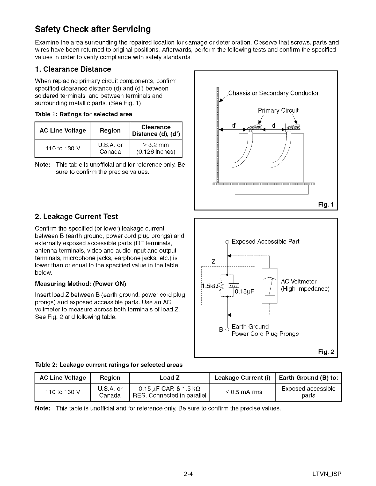
1. Clearance Distance
When replacing primary circuit components, confirm
specified clearance distance (d) and (d') between
soldered terminals, and between terminals and
surrounding metallic parts. (See Fig. 1)
Table 1: Ratings for selected area
Clearance
AC Line Voltage Region Distance (d), (d')
U.S.A. or > 3.2 mm
110 to 130 V Canada (0.126 inches)
Note: This table is unofficial and for reference only. Be
sure to confirm the precise values.
2. Leakage Current Test
Confirm the specified (or lower) leakage current
between B (earth ground, power cord plug prongs) and
externally exposed accessible parts (RF terminals,
antenna terminals, video and audio input and output
terminals, microphone jacks, earphone jacks, etc.)is
lower than or equal to the specified value in the table
below.
Measuring Method: (Power ON)
Insert load Z between B (earth ground, power cord plug
prongs) and exposed accessible parts. Use an AC
voltmeter to measure across both terminals of load Z.
See Fig. 2 and following table.
Chassis or Secondary Conductor
Primary Circuit
d'
Exposed Accessible Part
Z
il k"i ..............i
L............ I
Fig. 1
B Earth Ground
_AC Voltmeter
(High Impedance)
Power Cord Plug Prongs
Fig. 2
Table 2: Leakage current ratings for selected areas
AC Line Voltage Region Load Z Leakage Current (i) Earth Ground (B) to:
110to 130V U.S.A. or 0.15 pF CAP. & 1.5 k_ i _<0.5 mA rms Exposed accessible
Canada RES. Connected in parallel parts
Note: This table is unofficial and for reference only. Be sure to confirm the precise values.
2-4 LTVN_ISP
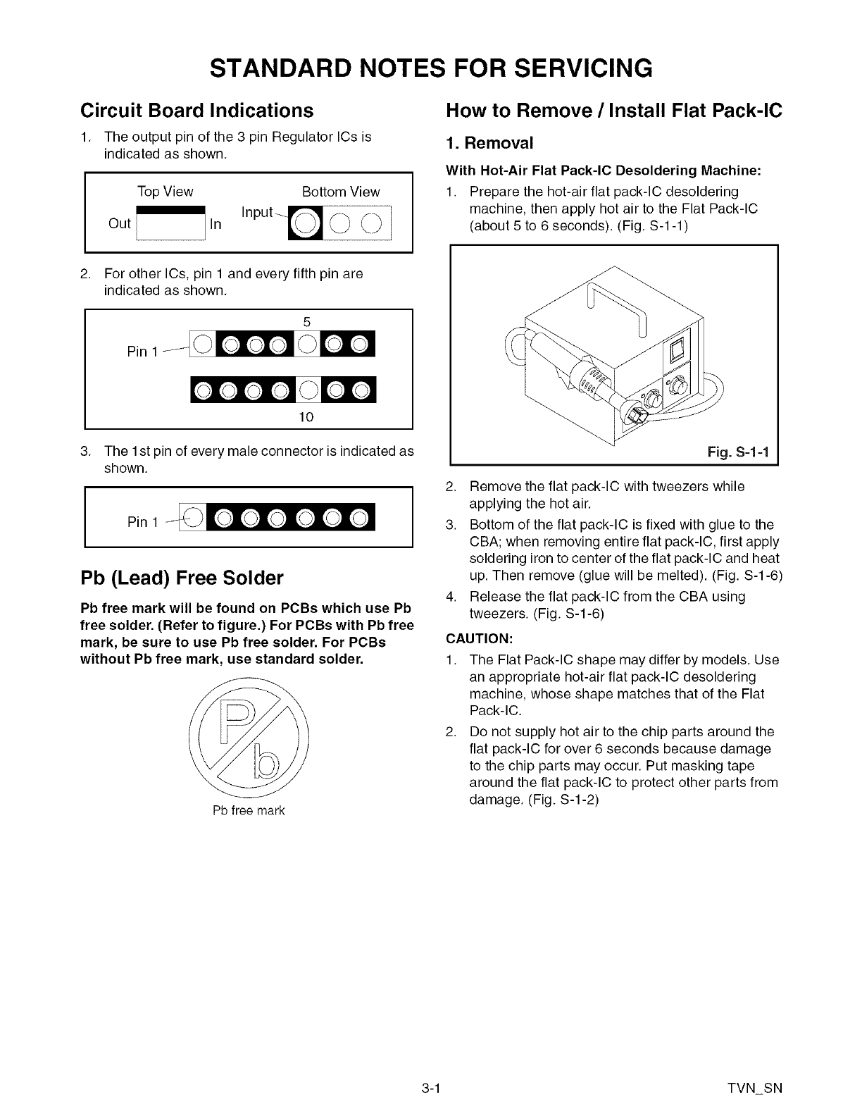
STANDARD NOTES FOR SERVICING
Circuit Board Indications
1. The output pin of the 3 pin Regulator ICs is
indicated as shown.
Top View Bottom View
Input_ _
How to Remove /Install Flat Pack-IC
1. Removal
With Hot-Air Flat Pack-IC Desoldering Machine:
1. Prepare the hot-air flat pack-IC desoldering
machine, then apply hot air to the Flat Pack-IC
(about 5 to 6 seconds). (Fig. S-1-1 )
2. For other ICs, pin 1 and every fifth pin are
indicated as shown.
5
Pin 1
10
3. The 1st pin of every male connector is indicated as
shown.
IPin 1 I
Pb (Lead) Free Solder
Pb free mark will be found on PCBs which use Pb
free solder. (Refer to figure.) For PCBs with Pb free
mark, be sure to use Pb free solder. For PCBs
without Pb free mark, use standard solder.
Pb free mark
Fig. S=l =1
2. Remove the flat pack-IC with tweezers while
applying the hot air.
3. Bottom of the flat pack-IC is fixed with glue to the
CBA; when removing entire flat pack-IC, first apply
soldering iron to center of the flat pack-IC and heat
up. Then remove (glue will be melted). (Fig. S-1-6)
4. Release the flat pack-IC from the CBA using
tweezers. (Fig. S-1-6)
CAUTION:
1. The Flat Pack-IC shape may differ by models. Use
an appropriate hot-air flat pack-IC desoldering
machine, whose shape matches that of the Flat
Pack-IC.
2. Do not supply hot air to the chip parts around the
flat pack-IC for over 6 seconds because damage
to the chip parts may occur. Put masking tape
around the flat pack-IC to protect other parts from
damage. (Fig. S-1-2)
3-1 TVNSN
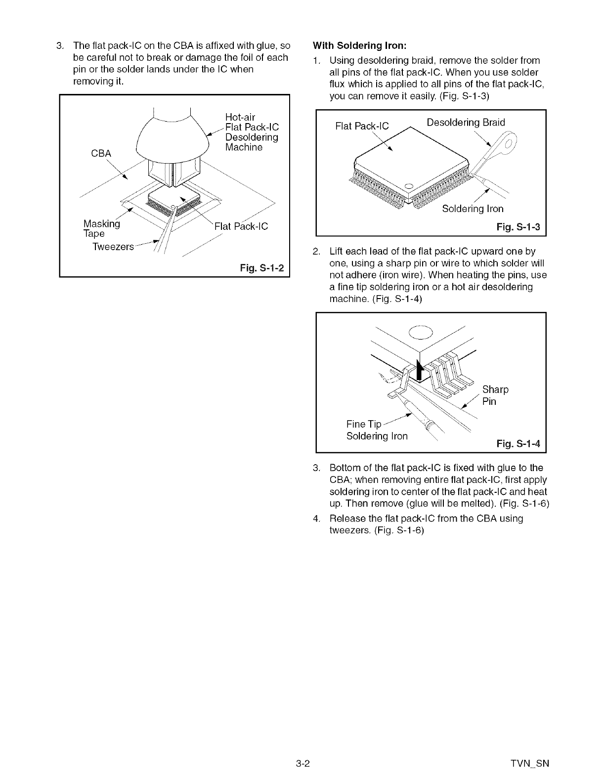
3. The flat pack-IC on the CBA is affixed with glue, so
be careful not to break or damage the foil of each
pin or the solder lands under the IC when
removing it.
CBA
\\
Masking
Tape
Hot-air
Pack-lC
Desoldering
Machine
Flat Pack-lC
Fig. S-1-2
With Soldering Iron:
1. Using desoldering braid, remove the solder from
all pins of the flat pack-IC. When you use solder
flux which is applied to all pins of the flat pack-IC,
you can remove it easily. (Fig. S-1-3)
Flat Pack-IC
\
Desoldering Braid
2.
Soldering Iron
Fig. S-1-3
Lift each lead of the flat pack-IC upward one by
one, using a sharp pin or wire to which solder will
not adhere (iron wire). When heating the pins, use
a fine tip soldering iron or a hot air desoldering
machine. (Fig. S-1-4)
Sharp
Fine Til
Soldering Iron Fig. S-1-4
3. Bottom of the flat pack-IC is fixed with glue to the
CBA; when removing entire flat pack-IC, first apply
soldering iron to center of the flat pack-IC and heat
up. Then remove (glue will be melted). (Fig. S-1-6)
4. Release the flat pack-IC from the CBA using
tweezers. (Fig. S-1-6)
3-2 TVNSN
WithIron Wire:
1. Using desoldering braid, remove the solder from
all pins of the flat pack-IC. When you use solder
flux which is applied to all pins of the flat pack-IC,
you can remove it easily. (Fig. S-1-3)
2. Affix the wire to a workbench or solid mounting
point, as shown in Fig. S-1-5.
3. While heating the pins using a fine tip soldering
iron or hot air blower, pull up the wire as the solder
melts so as to lift the IC leads from the CBA
contact pads as shown in Fig. S-1-5.
4. Bottom of the flat pack-IC is fixed with glue to the
CBA; when removing entire flat pack-IC, first apply
soldering iron to center of the flat pack-IC and heat
up. Then remove (glue will be melted). (Fig. S-1-6)
5. Release the flat pack-IC from the CBA using
tweeFers. (Fig. S-1-6)
Note: When using a soldering iron, care must be
taken to ensure that the flat pack-IC is not
being held by glue. When the flat pack-IC is
removed from the CBA, handle it gently
because it may be damaged if force is applied.
To Solid €
Mounting Point
Hot Air Blower
\\or
Iron Wir/
Soldering Iron
\ Fig. S-1-5
B_ Fine Tip
C Soldering Iron
\Flat Pack-IC
Fig. S-1-6
,
1.
2.
3.
Installation
Using desoldering braid, remove the solder from
the foil of each pin of the flat pack-IC on the CBA
so you can install a replacement flat pack-IC more
easily.
The "O" mark on the flat pack-IC indicates pin 1.
(See Fig. S-1-7.) Be sure this mark matches the 1
on the PCB when positioning for installation. Then
presolder the four corners of the flat pack-IC. (See
Fig. S-1-8.)
Solder all pins of the flat pack-IC. Be sure that
none of the _ins have solder bridges.
Example
Pin 1 of the Flat Pack-IC
is indicated by a "•" mark. Fig. S-1-7
Presolder
I
CBA
Flat Pack-IC
Fig. S-1-8
3-3 TVN_SN
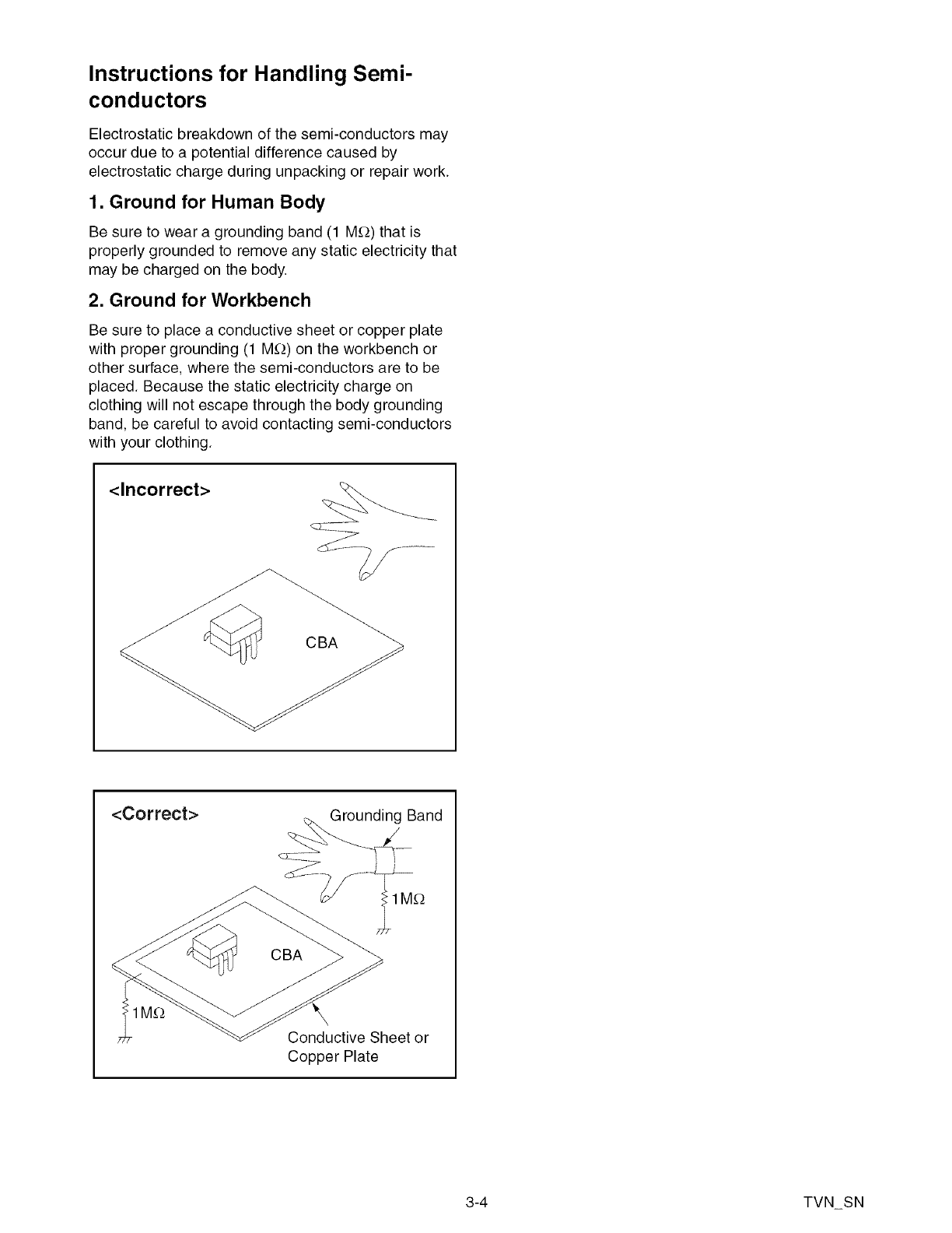
Instructions for Handling Semi-
conductors
Electrostatic breakdown of the semi-conductors may
occur due to a potential difference caused by
electrostatic charge during unpacking or repair work.
1. Ground for Human Body
Be sure to wear a grounding band (1 M_-_)that is
properly grounded to remove any static electricity that
may be charged on the body.
2. Ground for Workbench
Be sure to place a conductive sheet or copper plate
with proper grounding (1 M_) on the workbench or
other surface, where the semi-conductors are to be
placed. Because the static electricity charge on
clothing will not escape through the body grounding
band, be careful to avoid contacting semi-conductors
with your clothing.
<Incorrect>
CBA
<Correct> Grounding Band
Conductive Sheet or
Copper Plate
3-4 TVNSN
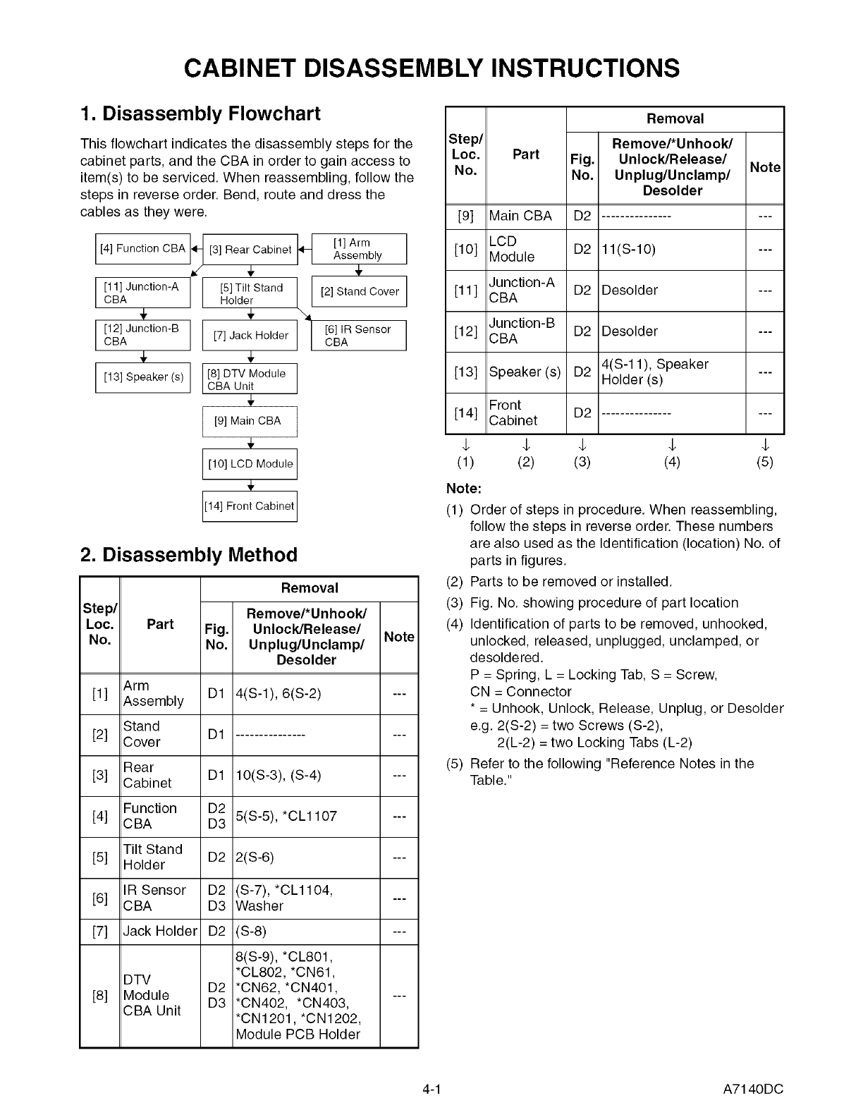
CABINET DISASSEMBLY INSTRUCTIONS
1. Disassembly Flowchart
This flowchart indicates the disassembly steps for the Step/
cabinet parts, and the CBA in order to gain access to Loc.
No,
item(s) to be serviced. When reassembling, follow the
steps in reverse order. Bend, route and dress the
cables as they were.
[ [4] Function CBA ]_[ [3] Rear Cabinet 1_ [1] Arm
Assembly
4, 4,
[11] Junction-A [5]Tilt Stand I I [2] Stand Cover
CaR /I Holder I I
4, 4, "4
[12] Junction-B [7] Jack Holder [6] IR SensorCBA CBA
4, 4,
[ [131Speaker(s)] [[8]DTVModuIe 1
/ CBA Unit I
[9] Main CBA
4,
[10] LCD Module
4,
[14] Front Cabinet
2. Disassembly Method
Step/
Loc.
No. Part
Arm
[1] Assembly
Stand
[2] Cover
Rear
[3] Cabinet
Function
[4] CBA
Tilt Stand
[5] Holder
IR Sensor
[6] CBA
[7] Jack Holder
[8] DTV
Module
CBA Unit
Fig.
No.
D1
D1
D1
D2
D3
D2
D2
D3
D2
D2
D3
Removal
Remove/*Unhook/
Unlock/Release/
Unplug/Unclamp/
Desolder
4(S-1 ), 6(S-2)
10(S-3), (S-4)
5(S-5), *CL1107
2(S-6)
(S-7), *CL1104,
Washer
(S-8)
8(S-9), *CL801,
*CL802, *CN61,
*CN62, *CN401,
*CN402, *CN403,
*CN1201, *CN1202,
Module PCB Holder
Note
Part
[9] Main CBA
[10] LCD
Module
[11] Junction-A
CBA
[12] Junction-B
CBA
[13] Speaker (s)
[14] Front
Cabinet
+ +
(1) (2)
Note:
(1)
Fig.
No.
D2
D2
D2
D2
D2
D2
+
(3)
Removal
RemovePUnhook/
Unlock/Release/
Unplug/Unclamp/
Desolder
11(S-lO)
Desolder
Desolder
4(S-11 ), Speaker
Holder (s)
Note
+ +
(4) (5)
Order of steps in procedure. When reassembling,
follow the steps in reverse order. These numbers
are also used as the Identification (location) No. of
parts in figures.
(2) Parts to be removed or installed.
(3) Fig. No. showing procedure of part location
(4) Identification of parts to be removed, unhooked,
unlocked, released, unplugged, unclamped, or
desoldered.
P = Spring, L = Locking Tab, S = Screw,
CN = Connector
* = Unhook, Unlock, Release, Unplug, or Desolder
e.g. 2(S-2) = two Screws (S-2),
2(L-2) = two Locking Tabs (L-2)
(5) Refer to the following "Reference Notes in the
Table."
4-1 A71 40DC
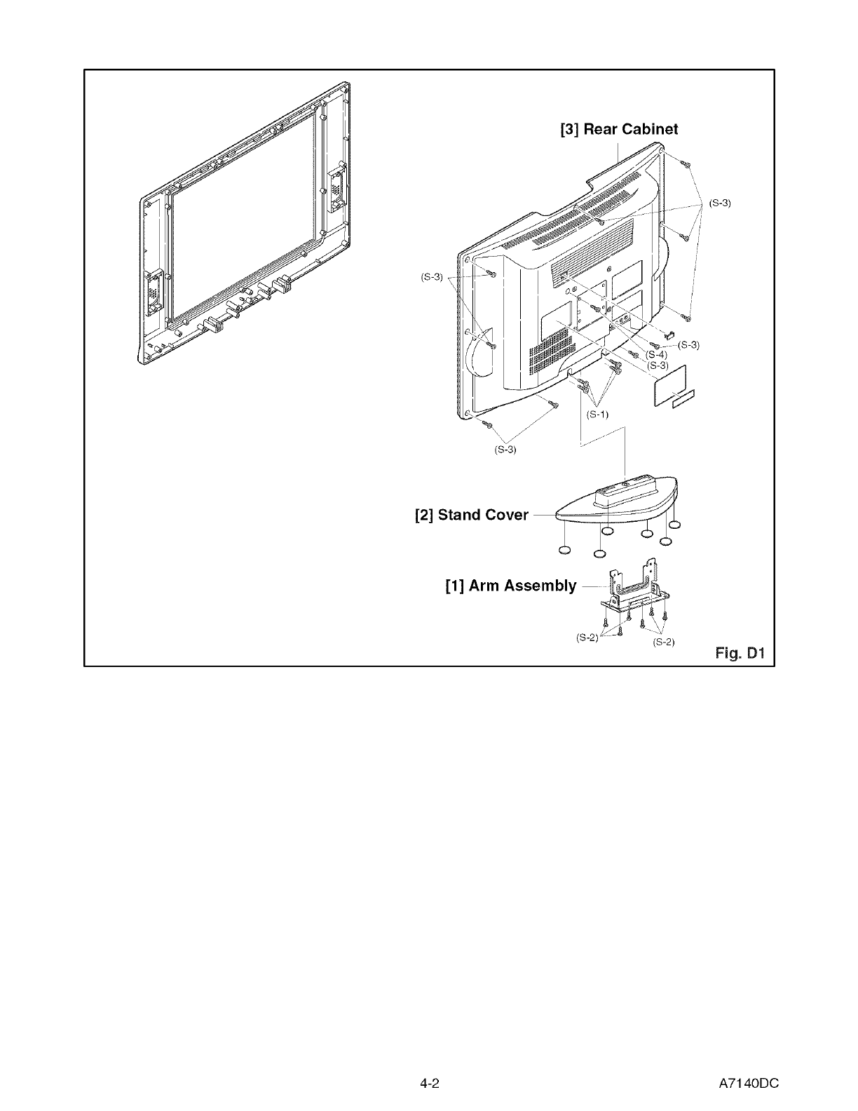
(s-3)
[3] Rear Cabinet
iI'
(s-3)
(S-1)
(s-3)
[2] Stand Cover _o_>'o o _
[1] Arm Assembly
(S_2)/_& _ (S__2)
Fig. D1
4-2 A71 40DC
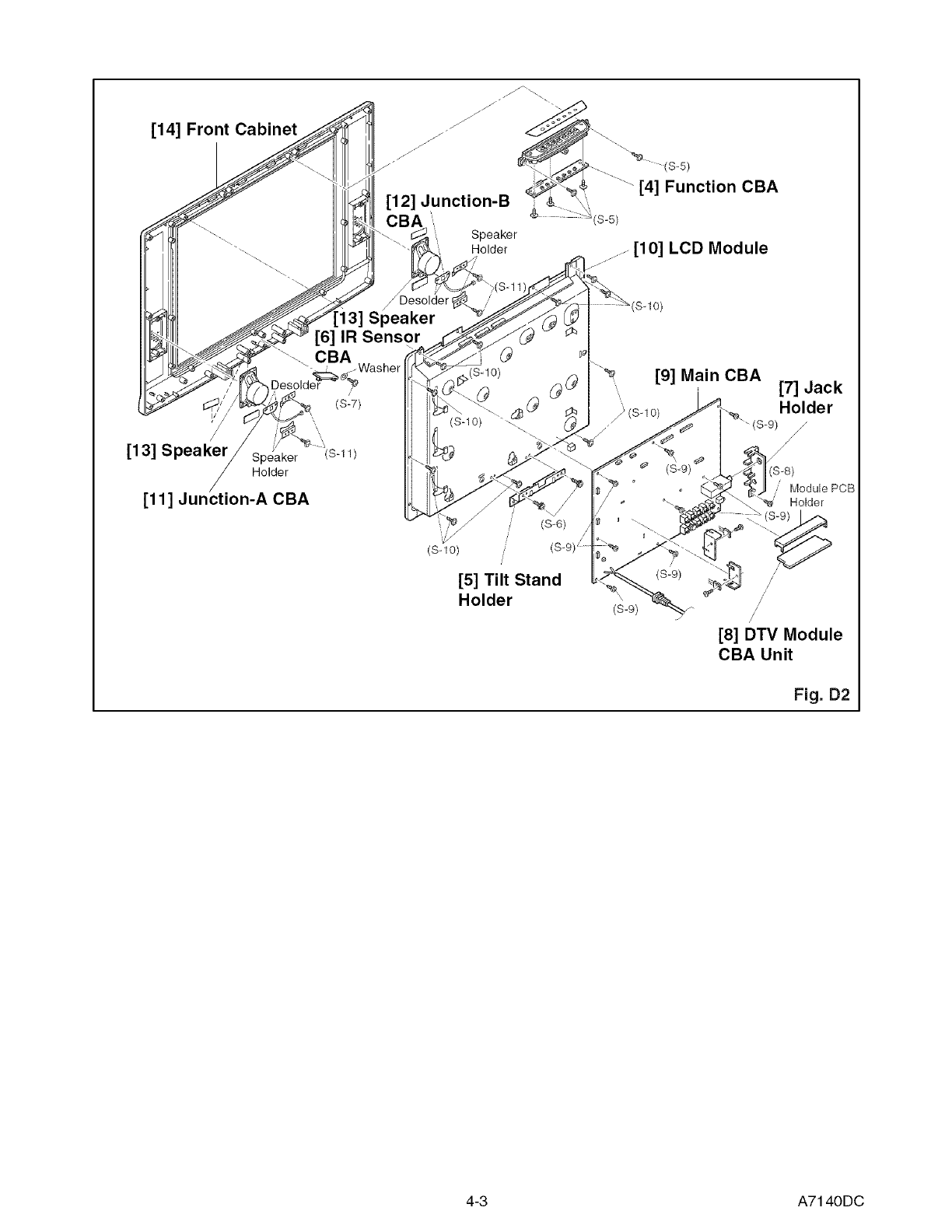
[14] Front Cabinet
[12] Junction-B
CBA
Speaker
Holder
Desolder
[13] Speaker
[6] IR Sensor
CBA
!/ //
[13] Speaker
[11]
Speaker
Holder
CBA
(S-11)
(s-6)
(sqo)
[5] Tilt Stand
Holder
(s-5)
(s-s)
[4] Function CBA
......[10] LCD Module
[9] Main CBA
,, [7] Jack
(s4o) Holder
/
Module PCB
Holder
(s=9)
/
(s-9) /
/
/
/
[8] DTV Module
CBA Unit
Fig. D2
4-3 A71 40DC
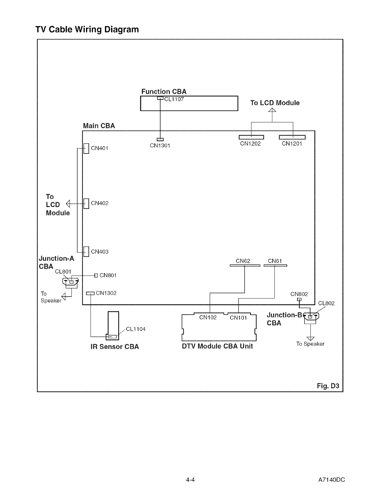
TV Cable Wiring Diagram
To
LCD _---
Module
Junction=A
CBA CL801
Main CBA
E] CN401
Function CBA
I I°"'°7
CN1301
I o LCD Module
CN1202 CN1201
F1 CN402
F] CN403
CN801
r- -_CN1302
m
i_ CL 1104
IR Sensor CBA
CN62
E
CN102
DTV Module CBA Unit
CN61
_ CN802
Junction=B_.)
CBA L_J
To Speaker
Fig. D3
4-4 A71 40DC
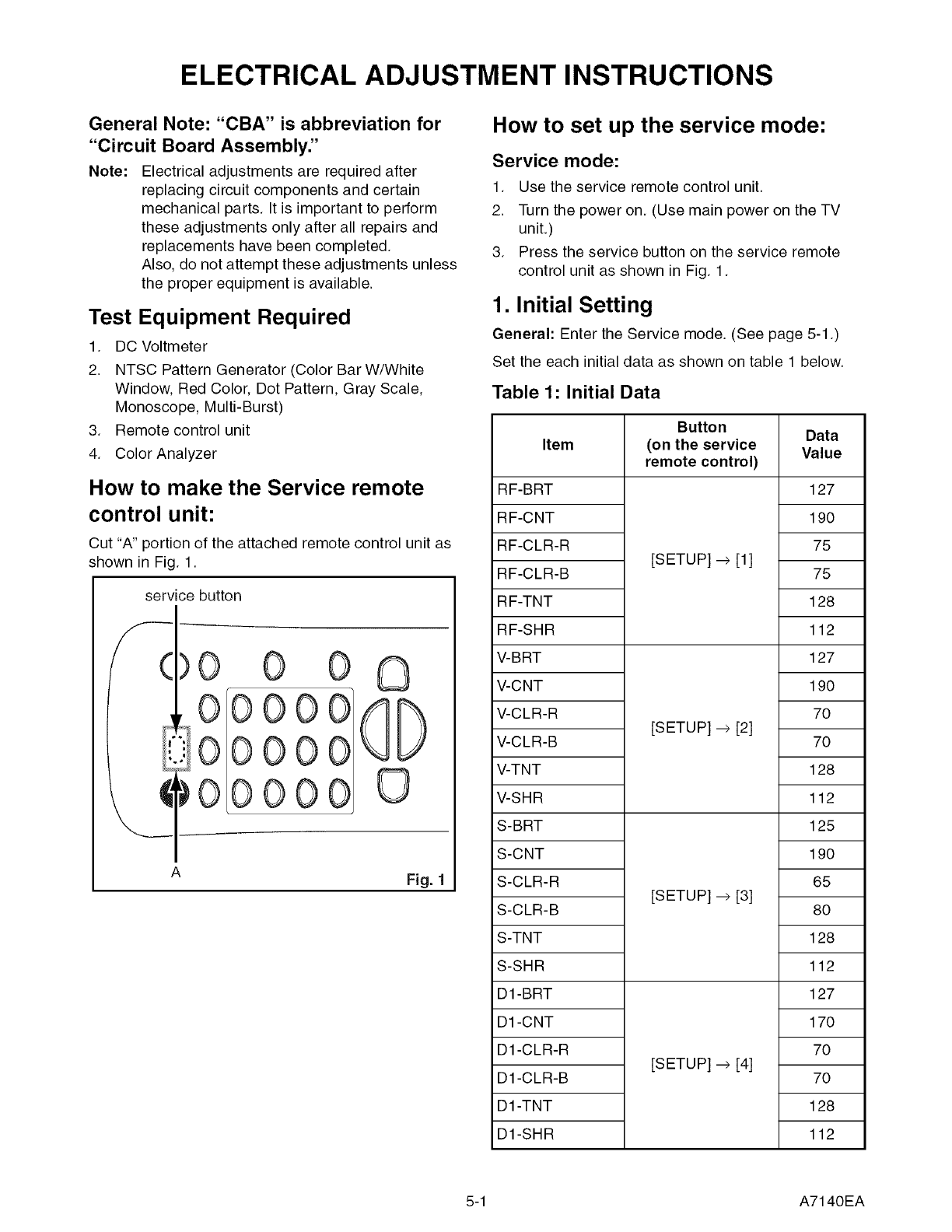
ELECTRICAL ADJUSTMENT INSTRUCTIONS
General Note: "CBA" is abbreviation for
"Circuit Board Assembly."
Note: Electrical adjustments are required after
replacing circuit components and certain
mechanical parts. It is important to perform
these adjustments only after all repairs and
replacements have been completed.
Also, do not attempt these adjustments unless
the proper equipment is available.
Test
1.
2.
3.
4.
Equipment Required
DC Voltmeter
NTSC Pattern Generator (Color Bar W/White
Window, Red Color, Dot Pattern, Gray Scale,
Monoscope, Multi-Burst)
Remote control unit
Color Analyzer
How to make the Service remote
control unit:
Cut "A" portion of the attached remote control unit as
shown in Fig. 1.
service button
)0 0 0
0000
0000
0000
G
(3
A Fig. 1
How to set up the service mode:
Service mode:
1. Use the service remote control unit.
2. Turn the power on. (Use main power on the TV
unit.)
3. Press the service button on the service remote
control unit as shown in Fig. 1.
1. Initial Setting
General: Enter the Service mode. (See page 5-1 .)
Set the each initial data as shown on table 1 below.
Table 1: Initial Data
Button
Item (on the service
remote control)
RF-BRT
RF-CNT
RF-CLR-R
RF-CLR-B
R F-TNT
RF-SHR
V-BRT
V-CNT
V-CLR-R
V-CLR-B
V-TNT
V-SHR
S-BRT
S-CNT
S-CLR-R
S-CLR-B
S-TNT
S-SHR
D1 -BRT
D1 -CNT
D1 -CLR-R
D1 -CLR-B
D1 -TNT
D1 -SHR
[SETUP] --> [1]
[SETUP] --> [2]
[SETUP] --> [3]
[SETUP] --> [4]
Data
Value
127
190
75
75
128
112
127
190
70
70
128
112
125
190
65
80
128
112
127
170
70
70
128
112
5-1 A7140EA
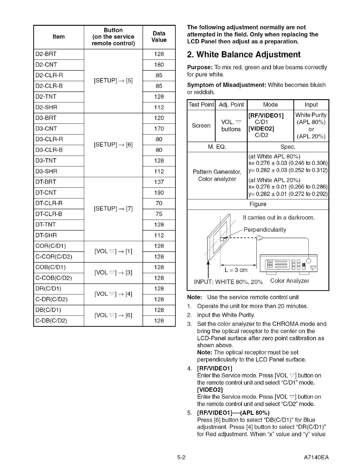
Button
Item (on the service
remote control)
D2-BRT
D2-CNT
D2-CLR-R
D2-CLR-B
D2-TNT
D2-SHR
D3-BRT
D3-CNT
D3-CLR-R
D3-CLR-B
D3-TNT
D3-SHR
DT-BRT
DT-CNT
DT-CLR-R
DT-CLR-B
DT-TNT
DT-SHR
COR(C/D1 )
C-COR(C/D2)
COB(C/D1 )
C-COB(C/D2)
DR(C/D1 )
C-DR(C/D2)
DB(C/D1 )
C-DB(C/D2)
[SETUP] --> [5]
[SETUP] --> [6]
[SETUP] --> [7]
[VOL _] --> [1]
[VOL _] --> [3]
[VOL _] --> [4]
[VOL _] --> [6]
Data
Value
128
180
85
85
128
112
120
170
80
80
128
112
137
190
70
75
128
112
128
128
128
128
128
128
128
128
The following adjustment normally are not
attempted in the field. Only when replacing the
LCD Panel then adjust as a preparation.
2. White Balance Adjustment
Purpose: To mix red, green and blue beams correctly
for pure white.
Symptom of Misadjustment: White becomes bluish
or reddish.
Test Point[ Adj. Point
Screen I VOL.
Ibuttons
M. EQ.
Pattern Generator,
Color analyzer
Mode
RF/VIDEO1]
C/D1 :]
C/D2
Input
White Purity
(APL 80%)
or
(APL 20%)
Spec.
(at White APL 80%)
x= 0.276 _+0.03 (0.246 to 0.306
= 0.282 _+0.03 (0.252 to 0.312
at White APL 20%)
i= 0.276 + 0.01 (0.266 to 0.286
y= 0.282 + 0.01 (0.272 to 0.292
Figure
L=3cm
INPUT: WHITE 80%, 20%
It carries out in a darkroom.
Perpendicularity
Color Analyzer
Note:
1.
2.
3.
4.
5.
Use the service remote control unit
Operate the unit for more than 20 minutes.
Input the White Purity.
Set the color analyzer to the CHROMA mode and
bring the optical receptor to the center on the
LCD-Panel surface after zero point calibration as
shown above.
Note: The optical receptor must be set
perpendicularly to the LCD Panel surface.
[RF/VIDEO1]
Enter the Service mode. Press [VOL _] button on
the remote control unit and select "C/D1" mode.
[VIDEO2]
Enter the Service mode. Press [VOL _] button on
the remote control unit and select "C/D2" mode.
[RF/VIDEO1]----(APL 80%)
Press [6] button to select "DB(C/D1)" for Blue
adjustment. Press [4] button to select "DR(C/D1)"
for Red adjustment. When "x" value and "y" value
5-2 A7140EA
arenotwithinspecification,adjust"DB(C/D1)"or
"DR(C/D1)".Referto "1.InitialSetting."
[RF/VIDEO1]----(APE20%)
Press[3]buttontoselect"COB(C/D1)"forBlue
adjustment.Press[1]buttontoselect"COR(C/
D1)"forRedadjustment.When"x"valueand"y"
valuearenotwithinspecification,adjust"COB(C/
D1)"or"COR(C/D1)'.Referto"1.InitialSetting."
6. [VIDEO2]----(APL80%)
Press[6]buttontoselect"C-DB(C/D2)"forBlue
adjustment.Press[4]buttontoselect"C-DR(C/
D2)"forRedadjustment.When"x"valueand"y"
valuearenotwithinspecification,adjust"C-DB(C/
D2)"or"C-DR(C/D2)'. Refer to "1. Initial Setting."
[VIDEO2]----(APL 20%)
Press [3] button to select "C-COB(C/D2)" for Blue
adjustment. Press [1] button to select "C-COR(C/
D2)" for Red adjustment.When "x" value and "y"
value are not within specification, adjust "C-
COB(C/D2)" or "C-COR(C/D2)'.
Refer to "1. Initial Setting."
7. Turn the power off and on again. (Main power
button on the TV unit.)
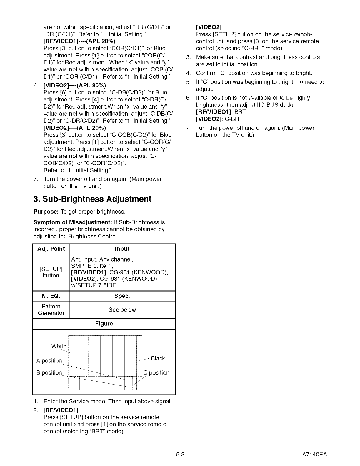
3. Sub-Brightness Adjustment
Purpose: To get proper brightness.
Symptom of Misadjustment: If Sub-Brightness is
incorrect, proper brightness cannot be obtained by
adjusting the Brightness Control.
Adj. Point Input
Ant. input, Any channel,
[SETUP] SMPTE pattern,
button [RF/VIDEO1]: CG-931 (KENWOOD),
[VIDEO2]: CG-931 (KENWOOD),
w/SETUP 7.51RE
M. EQ. Spec.
Pattern See below
Generator
Figure
[VIDE02]
Press [SETUP] button on the service remote
control unit and press [3] on the service remote
control (selecting "C-BRT" mode).
3. Make sure that contrast and brightness controls
are set to initial position.
4. Confirm "C" position was beginning to bright.
5. If "C" position was beginning to bright, no need to
adjust.
6. If "C" position is not available or to be highly
brightness, then adjust IIC-BUS dada.
[RF/VIDEO1]: BRT
[VIDEO2]: C-BRT
7. Turn the power off and on again. (Main power
button on the TV unit.)
1.
2.
White
Jalack
A position
C position
g position ........................................................................._ _ /
Enter the Service mode. Then input above signal.
[RF/VIDEO1]
Press [SETUP] button on the service remote
control unit and press [1] on the service remote
control (selecting "BR-F' mode).
5-3 A7140EA
HOW TO INITIALIZE THE LCD TELEVISION
How to initialize the LCD television:
1. Turn the power on. (Use main power on the TV
unit.)
2. To enter the service mode, press the service
button on the service remote control unit. (Refer to
page 5-1 .)
- To cancel the service mode, press [POWER]
button on the remote control.
3. To initialize the LCD television, press [DISPLAY]
button on the remote control unit.
4. Confirm "FF" indication on the upper right of the
screen.
6-1 A71201NT
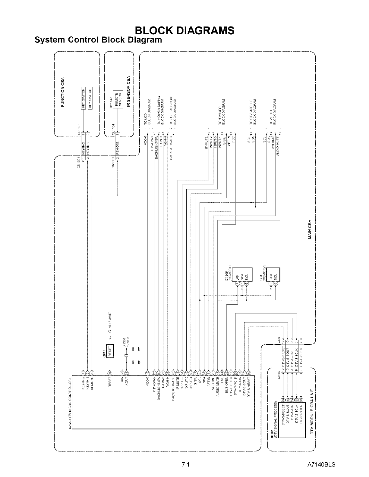
BLOCK DIAGRAMS
System Control Block Diagram
o
J
7-1 A7140BLS
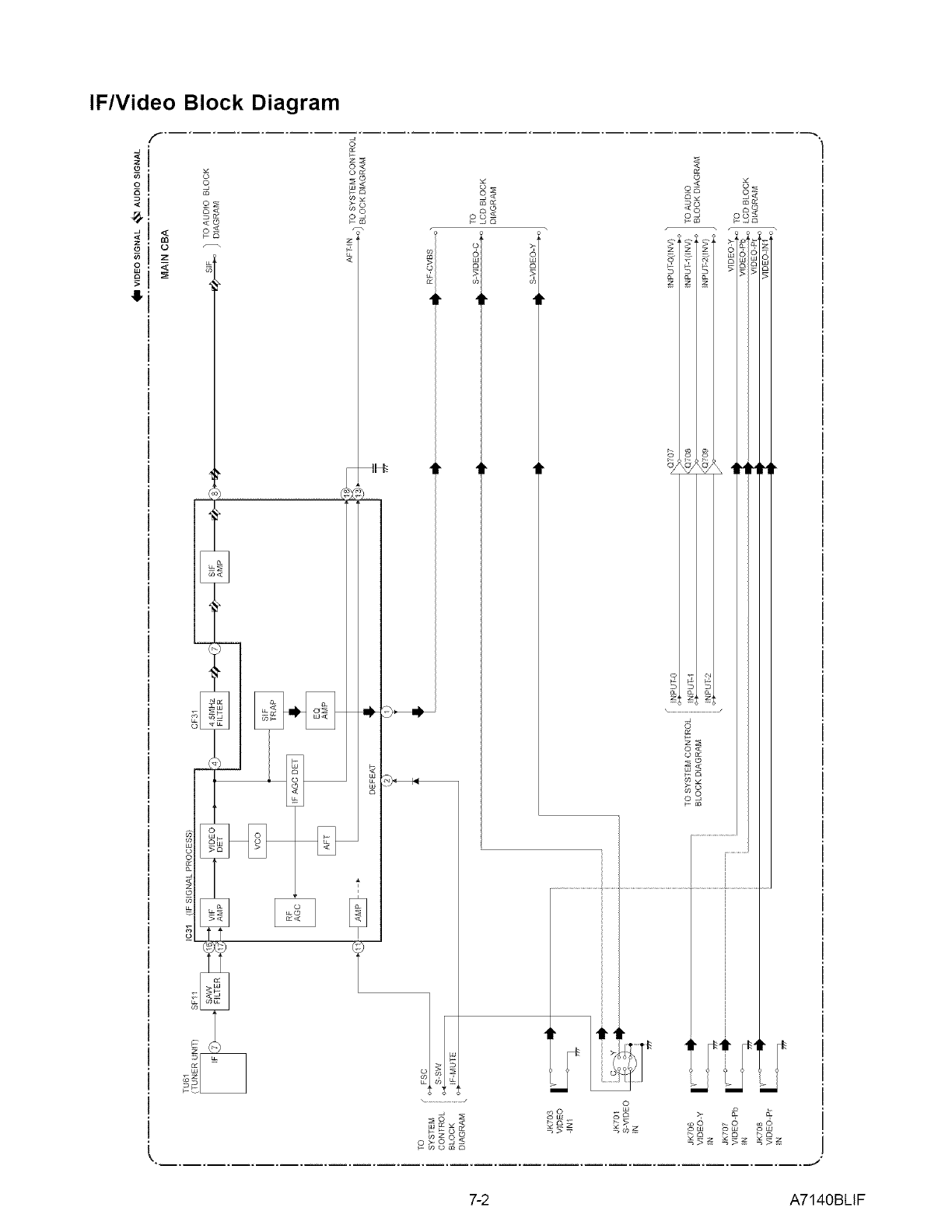
IF/Video Block Diagram
o
41-
0
z
<
$
@o _o _o
ow ow o_
ha _
7-2 A7140BLIF
Audio Block Diagram
f
el
<
o
I
h]o< o
L_
CO
0 "_
}
÷
)
o<I
_oL_
s
w_
_o _
oO_
/.............................\ .....................\
8
8
<3
m
L_
z
_o u_o _o oo
7-3 A7140BLA
DTV Module Block Diagram
"xI
'/ I
ii I
Ii
Ii i
i
i
i
i
i
i
i
i
i
i
i
i
i
Z
8
° i
o
i
i
i
i
(J
7-4 A7140BLDTV
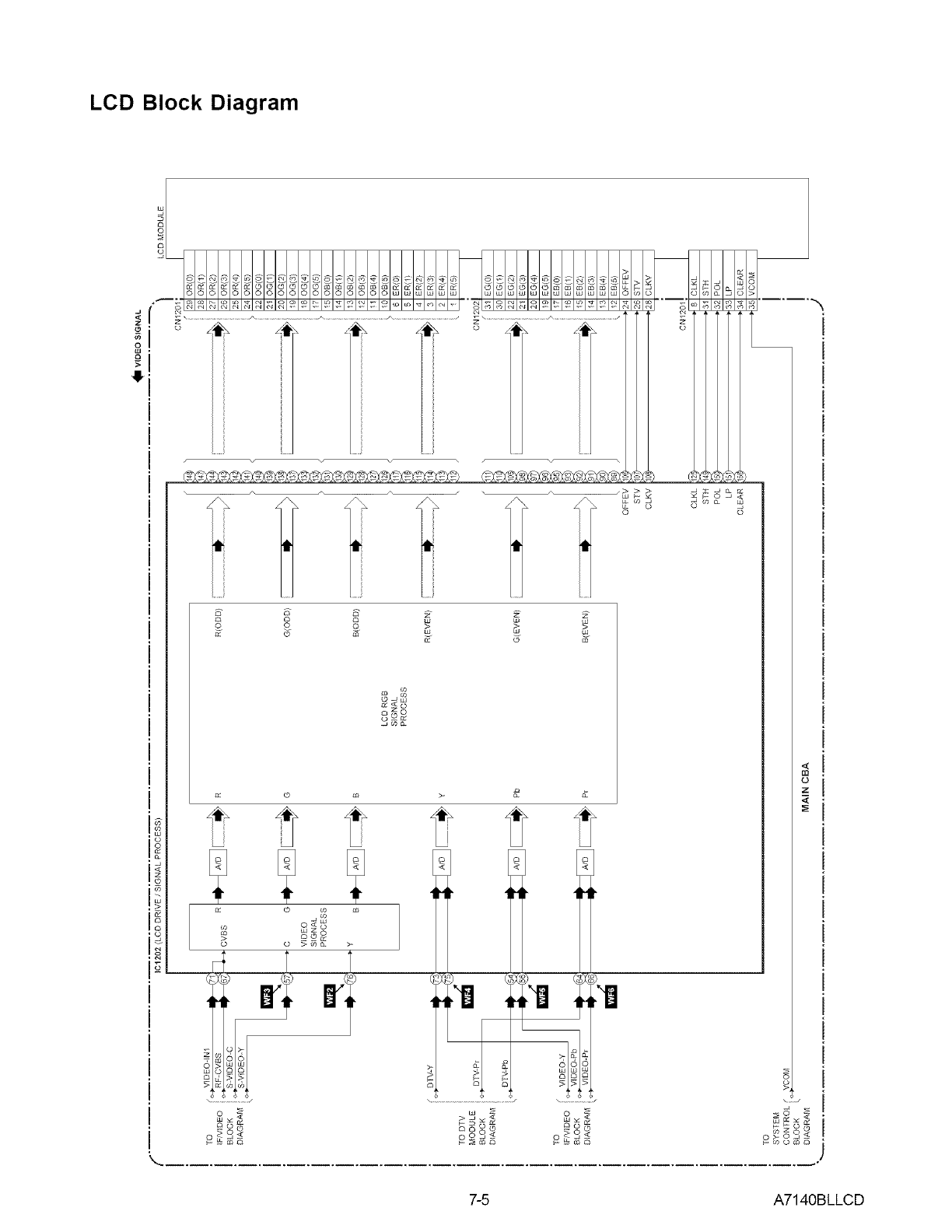
LCD Block Diagram
o
©
2
u_
2
©
2
uJ
8
_0_
tt
z_ ____
o _
o_9_
:>>:>
LU_d
8 °
d j:
d _- _
o
_o
wm
_z
o>-O
7-5 A7140BLLCD
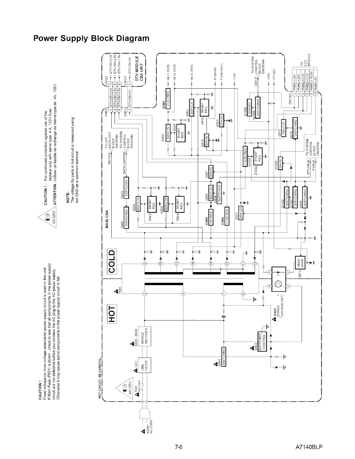
Power Supply Block Diagram
_ _ >_
s<-@
o_ c
o_: _
_o_
_5
"" z
zo
0 t--
>,
_S_
o o
o°_
_g
N_°E
E
_ c
_c
0) co
>0
b-x::
I
F%-
7-6 A7140BLP
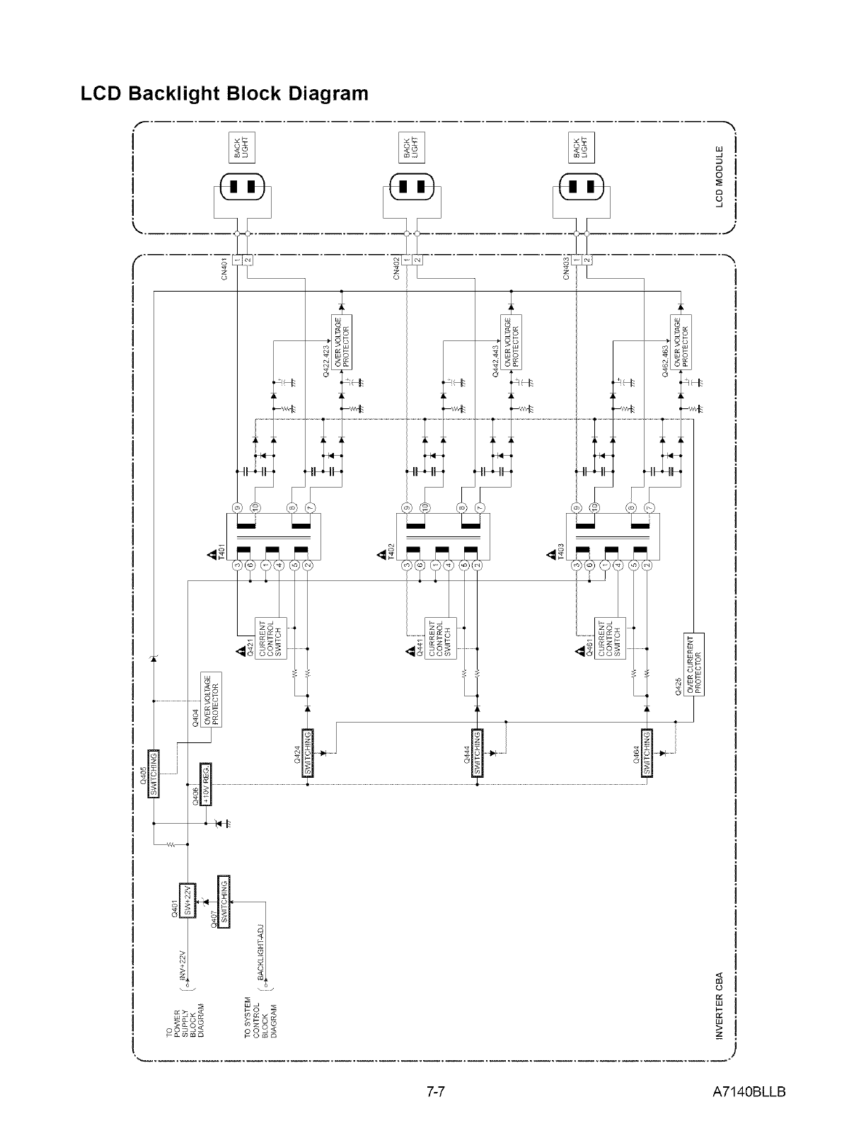
LCD Backlight Block Diagram
f
i
I
I
LU
.J
£3
0
£3
\__J \__J
wJ
_o
00_
w
>
z
7-7 A7140BLLB
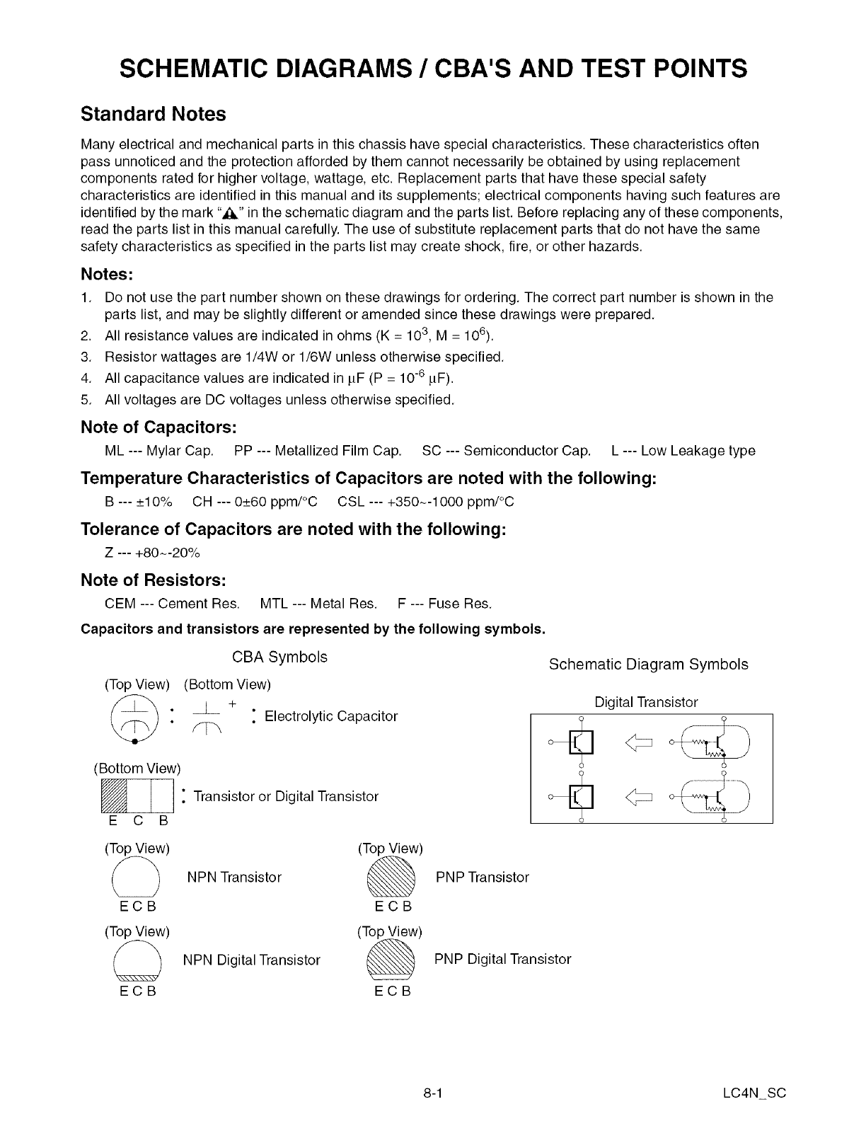
SCHEMATIC DIAGRAMS /CBA'S AND TEST POINTS
Standard Notes
Many electrical and mechanical parts in this chassis have special characteristics. These characteristics often
pass unnoticed and the protection afforded by them cannot necessarily be obtained by using replacement
components rated for higher voltage, wattage, etc. Replacement parts that have these special safety
characteristics are identified in this manual and its supplements; electrical components having such features are
identified by the mark ",_l&"in the schematic diagram and the parts list. Before replacing any of these components,
read the parts list in this manual carefully. The use of substitute replacement parts that do not have the same
safety characteristics as specified in the parts list may create shock, fire, or other hazards.
2.
3.
4.
5.
Note of Capacitors:
ML --- Mylar Cap. PP --- Metallized Film Cap. SC --- Semiconductor Cap.
Notes:
1. Do not use the part number shown on these drawings for ordering. The correct part number is shown in the
parts list, and may be slightly different or amended since these drawings were prepared.
All resistance values are indicated in ohms (K = 103, M = 106).
Resistor wattages are 1/4W or 1/6W unless otherwise specified.
All capacitance values are indicated in luF (P = 10 -6 pF).
All voltages are DC voltages unless otherwise specified.
L --- Low Leakage type
Temperature Characteristics of Capacitors are noted with the following:
B --- +10% CH --- 0+60 ppm/°C CSL --- +350--1000 ppm/°C
Tolerance of Capacitors are noted with the following:
Z --- +80--20%
Note of Resistors:
CEM --- Cement Res. MTL --- Metal Res. F --- Fuse Res.
Capacitors and transistors are represented by the following symbols.
CBA Symbols
(Top View) (Bottom View)
_ + °Electrolytic Capacitor/qm
(Bottom View)
_" or Digital
Transistor Transistor
E C B
Schematic Diagram Symbols
Digital Transistor
ECB
(Top View)
d2
ECB
NPN Transistor
NPN Digital Transistor
ECB
ECB
PNP Transistor
PNP Digital Transistor
8-1 LC4N SC
LIST OF CAUTION, NOTES, AND SYMBOLS USED IN THE SCHEMATIC DIAGRAMS ON
THE FOLLOWING PAGES:
1. CAUTION:
CAUTION: FOR CONTINUED PROTECTION AGAINST RISK OF FIRE, REPLACE ONLY WITH SAME
TYPE A, VFUSE.
ATTENTION: UTILISER UN FUSIBLE DE RECHANGE DE Me:ME TYPE DE A, V.
2. CAUTION:
Fixed Voltage (or Auto voltage selectable) power supply circuit is used in this unit.
If Main Fuse (F601) is blown, first check to see that all components in the power supply circuit are not
defective before you connect the AC plug to the AC power supply. Otherwise it may cause some components
in the power supply circuit to fail.
3. Note:
1. Do not use the part number shown on the drawings for ordering. The correct part number is shown in the
parts list, and may be slightly different or amended since the drawings were prepared.
2. To maintain original function and reliability of repaired units, use only original replacement parts which are
listed with their part numbers in the parts list section of the service manual.
4. Voltage indications on the schematics are as shown below:
Plug the TV power cord into a standard AC outlet.:
(Unit: Volt) *- - Power on mode
/
Voltage Indicates that the voltage
is not consistent here.
5. How to read converged lines
1-D3
L istinction Area
Line Number
(1 to 3 digits)
Examples:
1. "1-D3" means that line number "1" goes to the line number
"1" of the area "D3".
2. "1-B1" means that line number "1" goes to the line number
"1" of the area "B1 ".
3
2
m
1
i i
_ h[CC_
ARE
AREA B1
Ac I D
i
I
6. Test Point
©
cc}->
©
O
Information
: Indicates a test point with a jumper wire across a hole in the PCB.
: Used to indicate a test point with a component lead on foil side.
: Used to indicate a test point with no test pin.
: Used to indicate a test point with a test pin.
8-2 LC4N SC
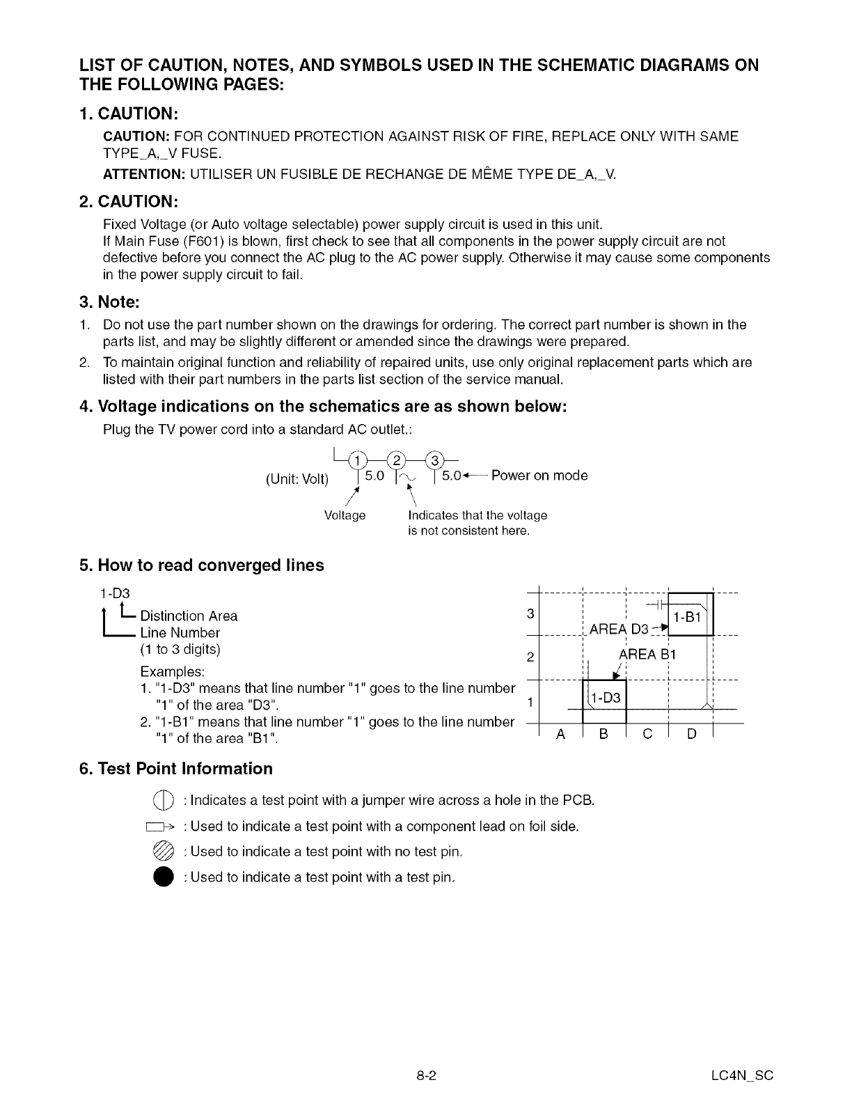
Main 1/5 Schematic Diagram
2
1
i
,) Fig OS
C8_ t _07,
/?0 I_a
',CSA CI_04 /IC'_fS02 i/30/
I
I
i
_,f_O_ll_UE '_
:Rt24a
22K
'1(}7
33
I 30_
33
,_i_
iii
olio_
1C_202
/LeD 8_IVE/
\ I, ¸ _ICI:_O
A I B
__ii i7_7_7_ ....... 7_i:_
,_
' _--"_' i i_ ....._ _ .........._--
I I BJ
i R 8 8
= EVEN ............
i
i
Pr _ .... 10 _ ...................................................................................................................
Pb _ A/O _ .... ,
s_ioi i i
8
b SIGNAL PROCESS
!_ /LCD DRIVE CIRCUIT
Y i¸x)i_
VIDEO SIONAL
PROCESS
041 31 33434 ti3]
ioi< i
_c_313 R_S_5 •
TO
!4 4 o
i
E!l
ii
4.
I
C±S39 ±
c 330 o { i
t1364 ,K
q 4 >o 1!3' 2K
_s52
4 7;<
IC_a05
5R24L64_WE2
[MEMCRYJ
IOH
lUH
I
't ;q2_
/2;,0/_6', ¸ _.
A!020 77i i _i fl _r iL.I TOOl _1_
''_:_ _4_-_ _"_, :, iI;' _ _
17 = I -" _.;4 ol 1:_I_4 i
28C2,85 ' o_,_,K
_ c, ,;_ @....................... t...............
C I D I E
L¸ i }i } R{)
'{;ON i ]Nul
_AiF 2/5 /
/o; N
d4,_TF 3/5 /
!CONT '
=k_,AiN4/5 /
/5
,14,_iN 2/5 i
/CON]INUE '
_4_i_ !i/5 /
ic)s; [[i '
!CONTINUE',
tIIAIN _/5/
,is _;
14M_ 3/5/
F
VOLTAGE CHART
CN1201
Pin No, Voltage
1 1.2
2 1.0
3 0.8
4 0.7
5 1.0
6 1.4
7 0
8 1.2
9 O
10 1.2
11 0.7
12 0.5
13 0.7
14 1.3
15 1.1
16 O
17 1.2
18 0.9
19 0.7
20 0.7
21 1.3
22 1.3
23 O
24 1.2
25 1.0
26 0.9
27 0.8
28 1.0
29 1.4
30 0
31 O
32 1.7
33 0.3
34 3.4
35 1.7
CN1202
Pin No. Voltage
1 O
2 24.4
3 24.4
4 O
5 3.3
6 3.3
7 O
8 10.8
9 O
10 -6,2
11 O
12 1.2
13 0.7
14 0.5
15 0.7
16 1.3
17 1.1
18 0
19 1.2
20 0.9
21 0.7
22 0.8
23 O
24 0
25 0
26 O
27 0
28 2.1
29 0
30 1.3
31 1.3
32 0
33 O
8-3 A7140SCM 1
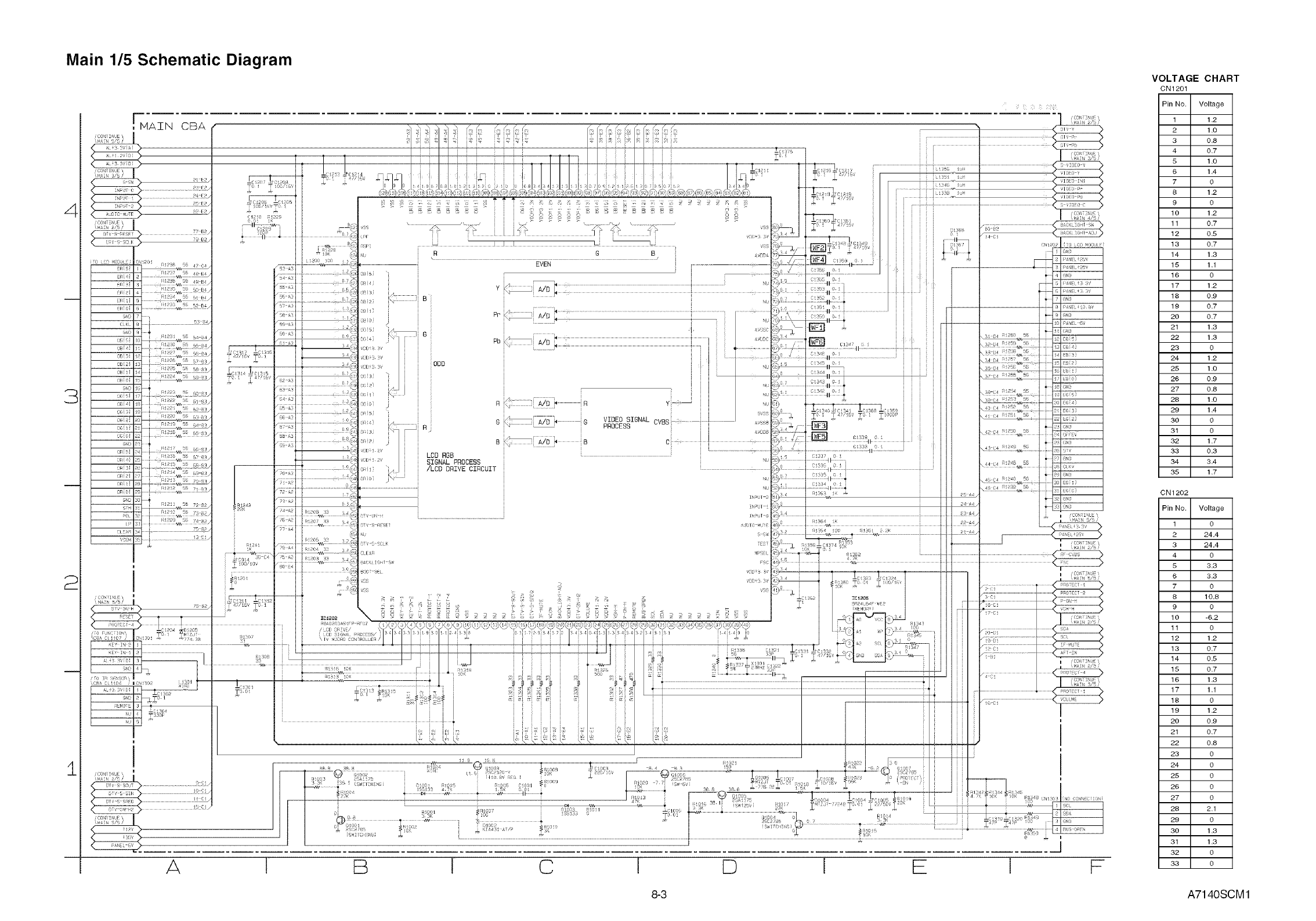
Main 2/5 Schematic Diagram
L
2
i
/CONTINUE
\_AIN W5 )
<I
i
P-ON+5V(J)
_ VT+33V
P ON_gV
I OTVDNF3,3 V
DTVON+_BV
DTV ON÷SSV
OTV ON+95V
DTVONli 8V
SMART ANT(NU)
A GNO
DIF OUT2
DfVVIOEO(NU)
DTV AUDIO{L)
OTV AUOIO[R)
ADNO
DTV-Y
DTV Pb
I
CONTINdE
I OTV-Y
DTVPP
DTVwPD
CONTINUE
(MAIN 1/5) I
SOt
IF N_
G
MAEN CBA
RBSJ
!DO
B852
_oo
ID851
AN5832SA_EJV
C860
10/50v
06B
JSS!33"
_O62 D63
I_SS_3S _SSIS3
03t
J_l !33
12C/PARA AGC MODE FOMO MUTE SIF/BB
LBSI
WIRE
C866
3SOP
8F3!
FILTER 45MHz
D34
R838
IPK
IDA52
TC4052BF(EINF]
(INPUT SELECT(
RB27 R885
_OOK _10OK
BC6!
BEAD
TUB1
TUNER UNiT
046
W!RE
:R49
'18K
_C84
SF11
SAFHS45M7VAOZOOSB05
:ii 7 ¸ k }(ii(i ¸
0807 J
_814
RBJ7 2PK
47K
!
J BC52
BAD
R6J 220
f:4s2 220
R67 0
RDO 0
I
iCONTINUE
(MAIN 3/5 )
AUDIO(L)-INi
AUDIO(R] INJ
AUD:[O(L) OU[
AUDIO(R)-OUT
CONTINUE
(MAIN 3/5)
AUDIO([( IN2
INPUT_O(INV)
INPUT J(INV]
INPU72(INV)
PONq9V
_TO DrY MODULE
_£BA UNIT ONiOn/
O GND
OfV SPO!F
DIV-ONiSV
TU SCI
TU SDA
OGNO
OTV S SREO
DTVSSCLK
DTV S SIN
OTV-S-SOUT
0 GNO
DIVSRESEI
D GND
SOA
SCL
DTV-S-SOUT I
DTV SSIN
D!V SSREQ
01V-ONH2
H T I d K
i
L
VOLTAGE CHART
CN61
Pin No. Voltage
1 0
2 1.1
3 5.2
4 3.1
5 3.2
6 0
7 2.9
8 3.2
9 1.7
10 0.1
11 0
12 3.4
13 0
14 3.1
15 3.1
CN62
Pin No. Voltage
1 ---
2 3.3
3 0
4 3.4
5 2.6
6 1.9
7 --
8 0
9 0
10 0
11 0
12 0
13 0
14 ---
15 2.6
16 2.6
17 0
18
19
20
8-4 A7140SCM2
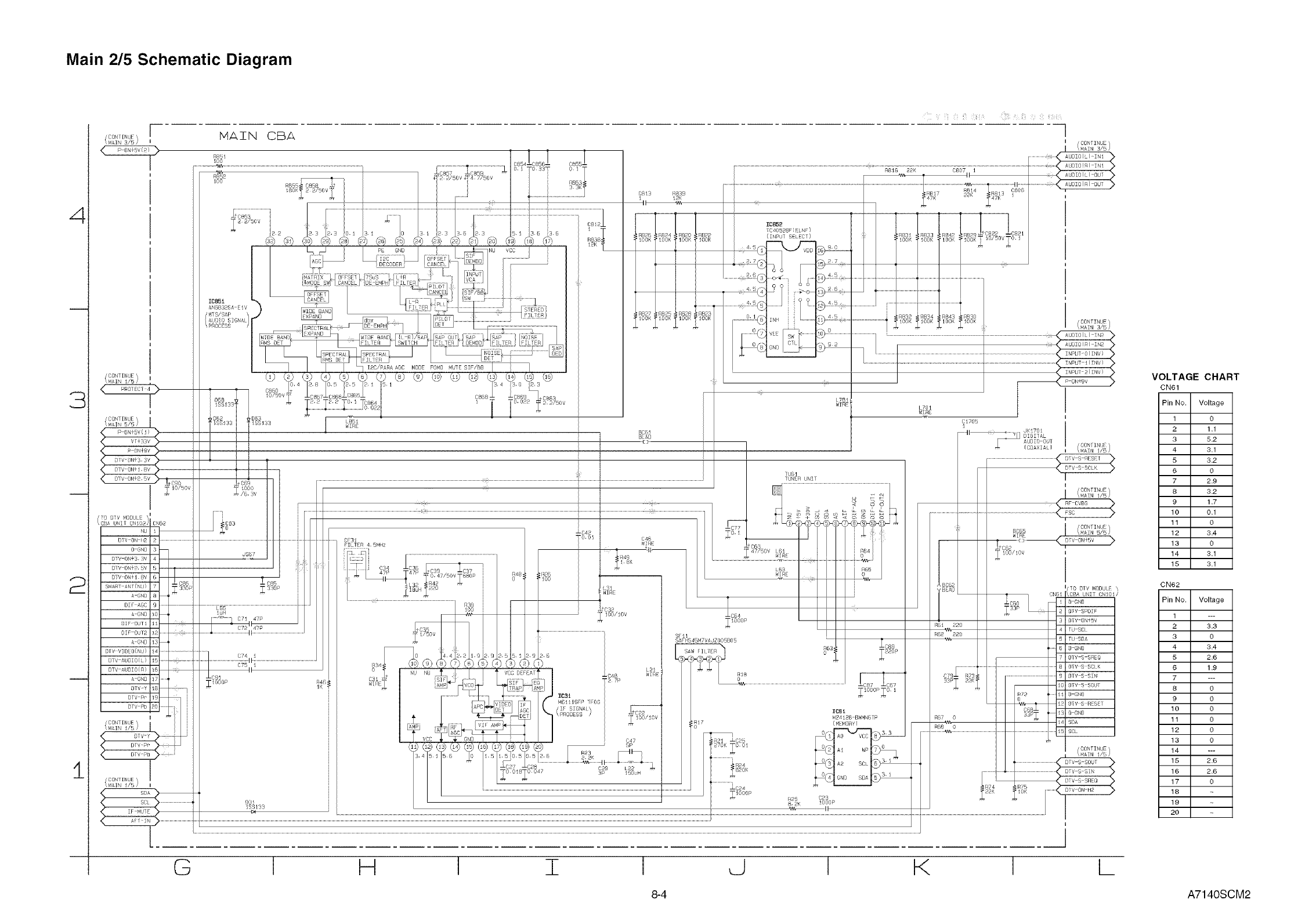
Main 3/5, Junction-A & Junction-B Schematic Diagram
L
3
2
1
(CONT!NUE_ F-----
_AiN 2/5/ C7_4 I
AUDIOIL) IN i ! C7_51_i ...........................................................................................................................................................................
AUDIOIR)AUDIOIL)OuTINI ....................................................................................................... 4_ ..................................................................................................................................... _................................................................................................................................
AUDIOIR)_OU_
VIDEO Pe ................................................................................................................................................................................................i.......................................................................... .............................
/
VISEOPb
SVIDEOC
A A
R807 R805
21 /_W 2I7/2W
/CONr NU_ _ ,_'/]803
\NAIN 1/5/ 0802 "{_M dl 776. P8
R81J
_0K
ICBOI
SA74i2
I
I
RSOB f:1837 RB40
CB23 2 214 IK
8 I = - "a;
_C809 tR809 07
10/50V 4 7K
Q802
2S02785 ) z !0750V
ABJ2
47K
,#
JS703
2SC2785
IINVER_I!R)
:R783
:_234
!O0
i.........
I J
[}}} ........................
10K
JS704 A738
O_ w /0_ 3
R810
,%
R739
J3705 !00
i j (i 9} ! A}( i{Xiui!L:4;i3} &!
iVlAZ N CBA
....
AUO!O R) IN2
INPUT O(INV
[NPUT I(INV)
INPUT 2(INV}
P 0Nq9V
R707
JS701 f00
R7f6
dS7O2 100
R2_B
82_
JKT03
VIDEO
IN/
_C786
ZZZZZZZZZZZZZZZI_N__o
.... INPUT I
_NPUT 2
AdOiO NUTE
............................................................................. d<70B
C751 _ R756
rvl I N O P o T F_
8-5 A7140SCM3
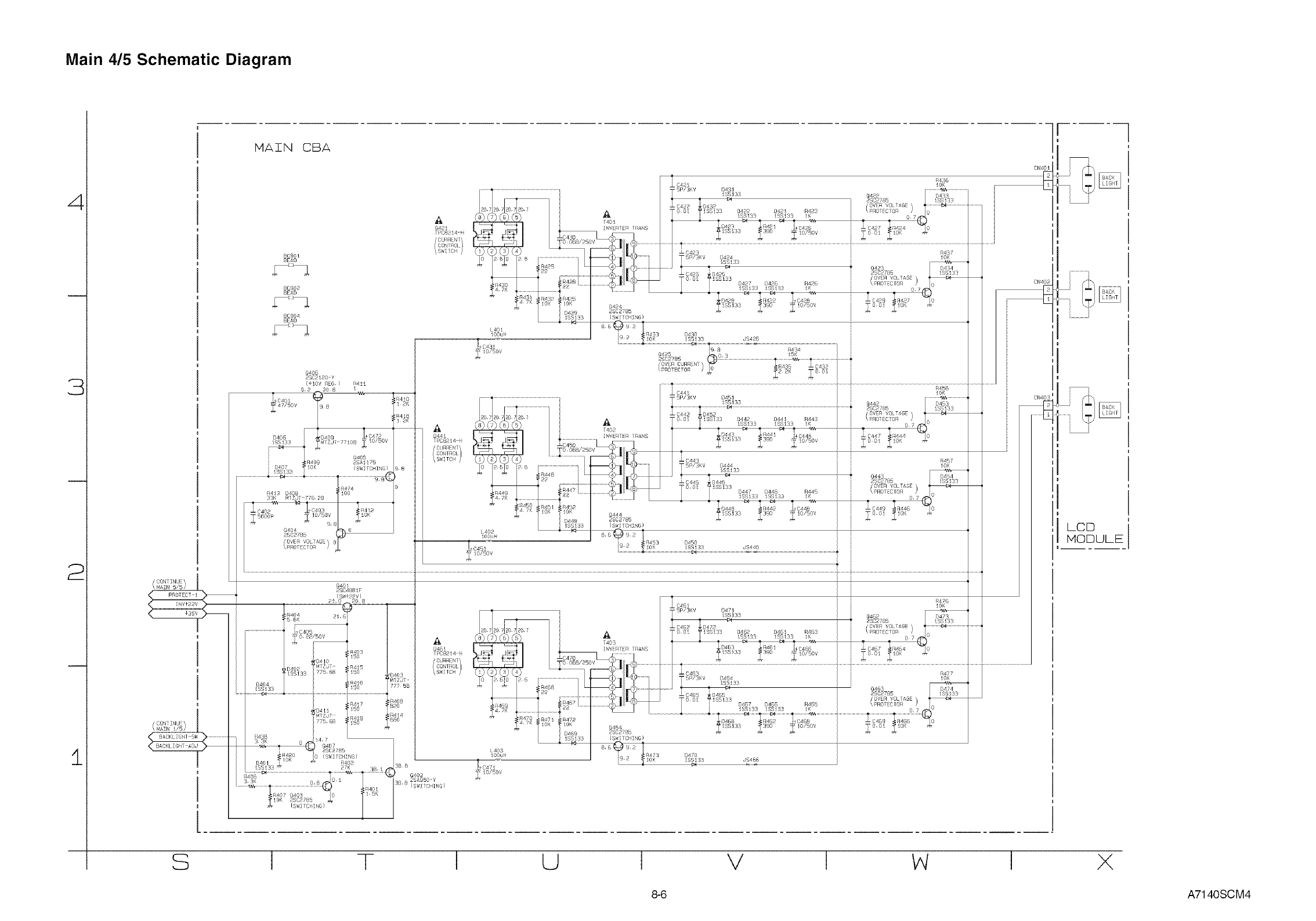
Main 4/5 Schematic Diagram
L
3
2
i
CONTINU£_
MAIN 5/57
PROTECT-_ _
INV+22V
+35V
CONTINUE]
MAIN !/5/
S
MATN CBA
BCgOl
BEAO
BCg04
BEAD
040B
8SCBJ2o Y
(k_OV REG / Rq!t
92 20 8 J
+c.oi !o
47/50V 9 8
D40i B409 +C472
- 7_8B
/ 0405
IR40g 28_/_7b
D407 3 1OK (SWTTC ING}
/SSJ3, U_
/
R413 D,108 JO
33K MTZdT 776 2B
-- 6402 _8403 P/412
_t 9 0_BOOP JO750V lOK
0VR vo AGE) (r_
T0R
T
CN40E
CN40E
CN403
LCD
NODULE
u I v I w I x
8-6 A71406CM4
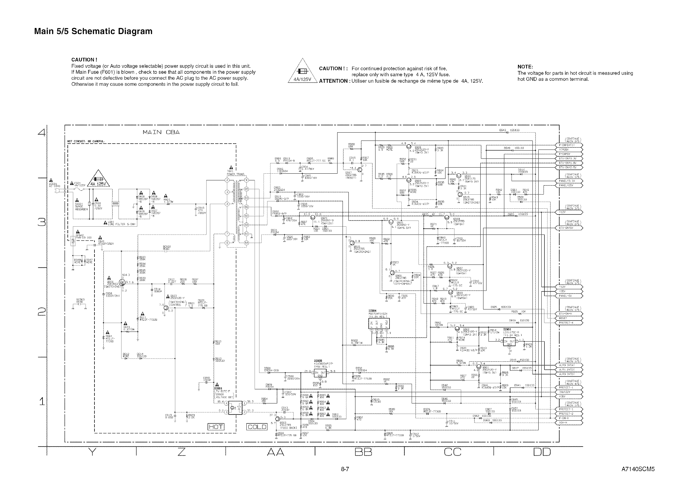
Main 5/5 Schematic Diagram
CAUTION !
Fixed voltage (or Auto voltage selectable) power supply circuit is used in this unit•
If Main Fuse (F601) is blown, check to see that all components in the power supply
circuit are not defective before you connect the AC plug to the AC power supply•
Otherwise it may cause some components in the power supply circuit to fail.
_4A/1_.25V'V_ CAUTION ! :For continued protection against risk of fire,
replace only with same type 4 A, 125V fuse.
, ATTENTION : Utiliser un fusible de rechange de m_me type de 4A, 125V.
NOTE:
The voltage for parts in hot circuit is measured using
hot GND as a common terminal.
Z
J
2
1
I
MATN CBA o_43_s,3_ ;
/CONE
HOT CIRCUIT. BE C_EFUL. \MAIN 2/5 )
RgOt B913 D905 R969:_ IOI C915 N_987 R93q _A
3.9 FR_04 R MTZOT- 777 5C _K O_ _OK 560= 1_ 931 DTV 0N43 3V >
C904 4 ,_ P F 4
T_9_.... '@_ _"_"_ I .... '0 ..... :_÷__'__4I ...... I '_'!_'_•__,_0.',
\HAIN !/5)
\
_5 J 2!:_}S04 R937 R996 0 33K _42 ogB 9!B --
C903 j) *
= SIHtG O 22 I L,s } } _O00/lOV r_ /_ CONTINUE
.... ,,°,,, .... _>
JI
L} + 20/_BV J2K ,Rg_ 4TZjT
.... I C64J r_ _ , 0 08 _OK 47K - _OZ5OV
........ BCCO) ..................... I 0 a96 , ,
_'390K " ( "I t 149_7 R928 S_HSV)
843 _ ,,'_r,_n_RqP4 I t z70 470
.m $ 390K 8612 R6O, _607 _ ........ _ P
0 C614 I "_M, 5 7 _ 5 2 ,/hv
I'I ..... , : ._Ill _' u, .... ",_
T IO00:_/!KV =_060_ = 4. _rlco __:S;-_ I I I _ 82sC2_20 Y } _PANEL BY
Begs3Q 2Sg2_20 Y D609 I _ 88K _4/P_47P _jd _1R98. R959 'SW+5V }
'f.zd 7x,aB I _ t I bg_,_ isss3 ; _ FCbET
,_ I 7_ <, I I I ;q9!9 _ _r L_F_ PNOTF_ 4PROT CT 4
Rc13 ....... _ i
S[ rlgB6 1.2K
_RE tSSt33 _ [ _
.................................................................?;_;. _ i,oo_ II .,oo _ _ /
'.... (5v REG D93_ ......................... FIgOi• Y ..........
ERC8 009 ", o 5 8 Q@4 4.0 88220 _1_ .................... ,, ALH_._VO] ]
,...... c_o_ _ , _?o _o_ _ _ >
_1_ I _:]09 I _50 • [R993 _ I D942 D9!5 mR909 D94_ 18S_33
Izc_o_ _ _4 _ .I'* _S:_K _ .I _,_ ,_ _A_ A/_,_oK _ ....................+
............... PROEC ! >
_v-_Tc_ I 1 !•c9o7 _ _ } *I _ ! } mv+_av >
I/ERROR / I / 7_tOO/50V _ReS A a'_<A I
I\VOLTAGE DET/ 954 I'+" t 5e_<_ T3°° _' I ID9_0 IlJ_4b !i]r)4 15V >
5 _8S±33 _o7/_ov ..........................................................................................................................................
W]So R955
R957 129;>8 +C 12 I
I
Y I TAA I BB ]CC I DD
8-7 A7140SCM5
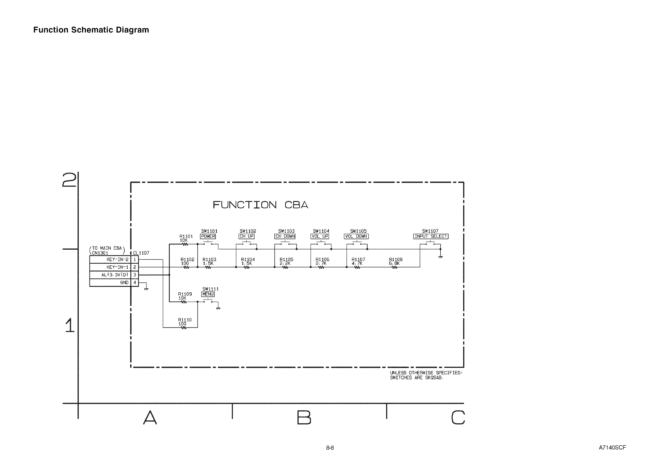
Function Schematic Diagram
2
l
TO MAIN CBA)
CNi30i
KEY-IN-2
KEY-IN-!
AL+3,3V(D)
GND
II
I swllo_ sw!t02 swil03 swll04 swi!05 swtt07 '
RiiOi _ [_ F_ r_ IVOL DOWN] IINPUT SELECT] I
iOK _ _ _ _ _
SW!I_t !
nito9 [_ I
IOK
1oo I I
J
I
UNLESS OTHER!4ISE SPECIFIEB=
SWITCHES ARE SKQSAB,
A B l C
8-8 A7140SCF
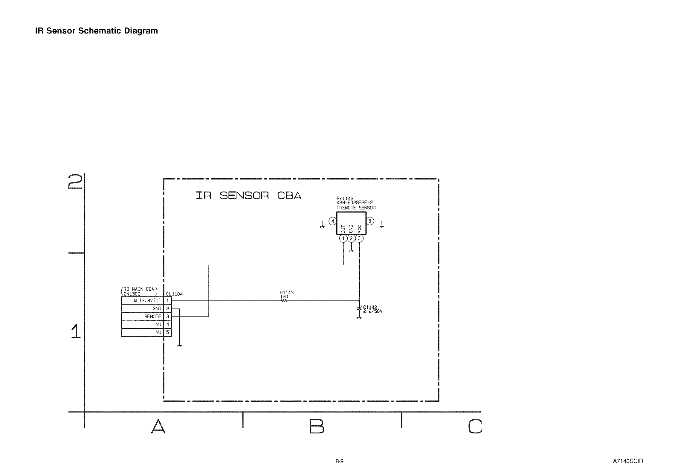
IR Sensor Schematic Diagram
1
TO MAIN CBA)
CN1302
AL+3.3V(D)
GNO
REMOTE
NU
NU
TR SENSOR CBA .v_ I
KSM-602SR2E-2
(RENOTE SENSOR) !
!
I
CLtI04 Rl143
_Ct142
'2.2/50V
I
'I
J,
' I
I ,
, __1
A1B C
8-9 A7140SCI R
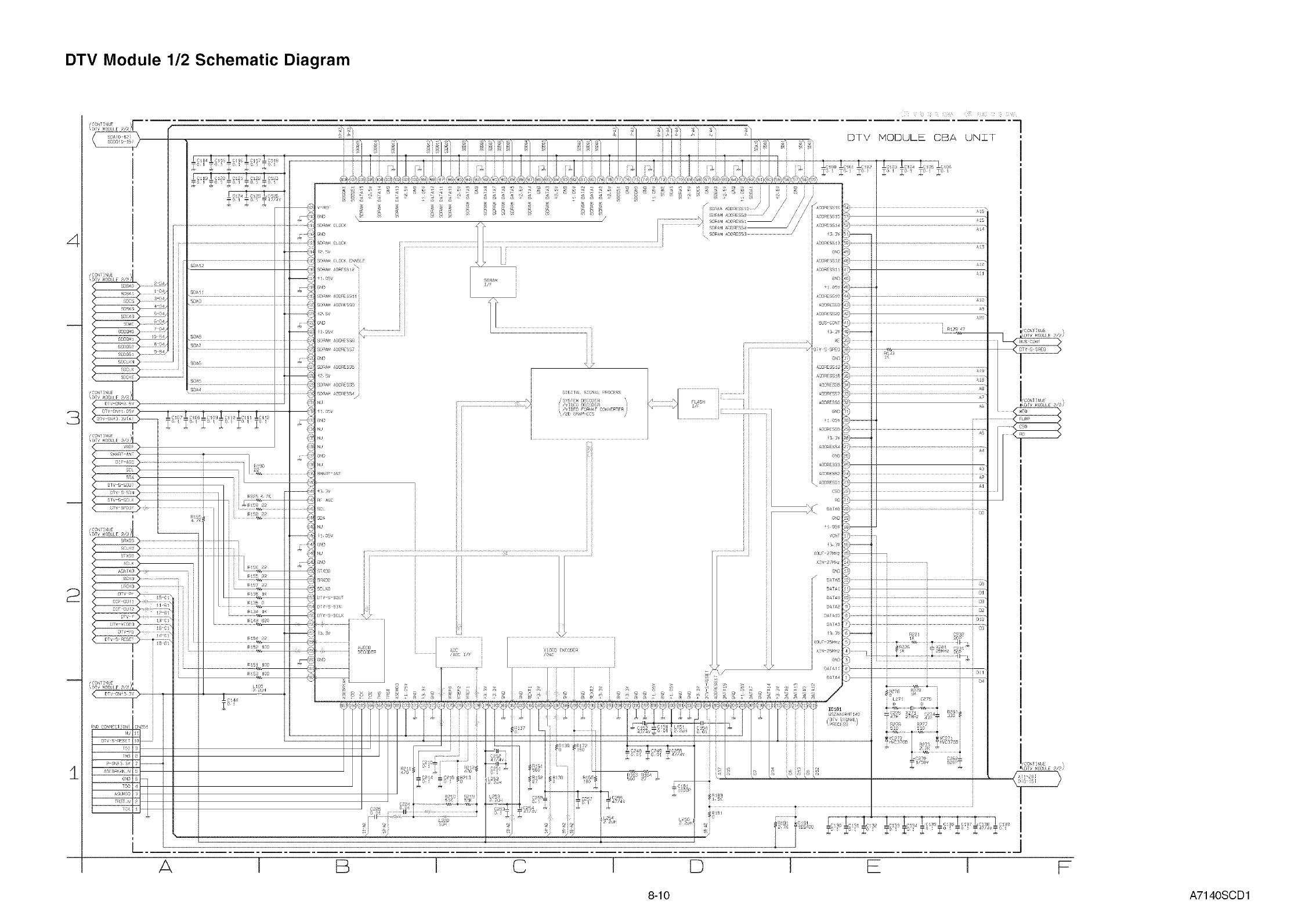
DTV Module 1/2 Schematic Diagram
l
2
1
H { 15F _ Fh_{ qk L ;kL
8-10 A7140SCD1
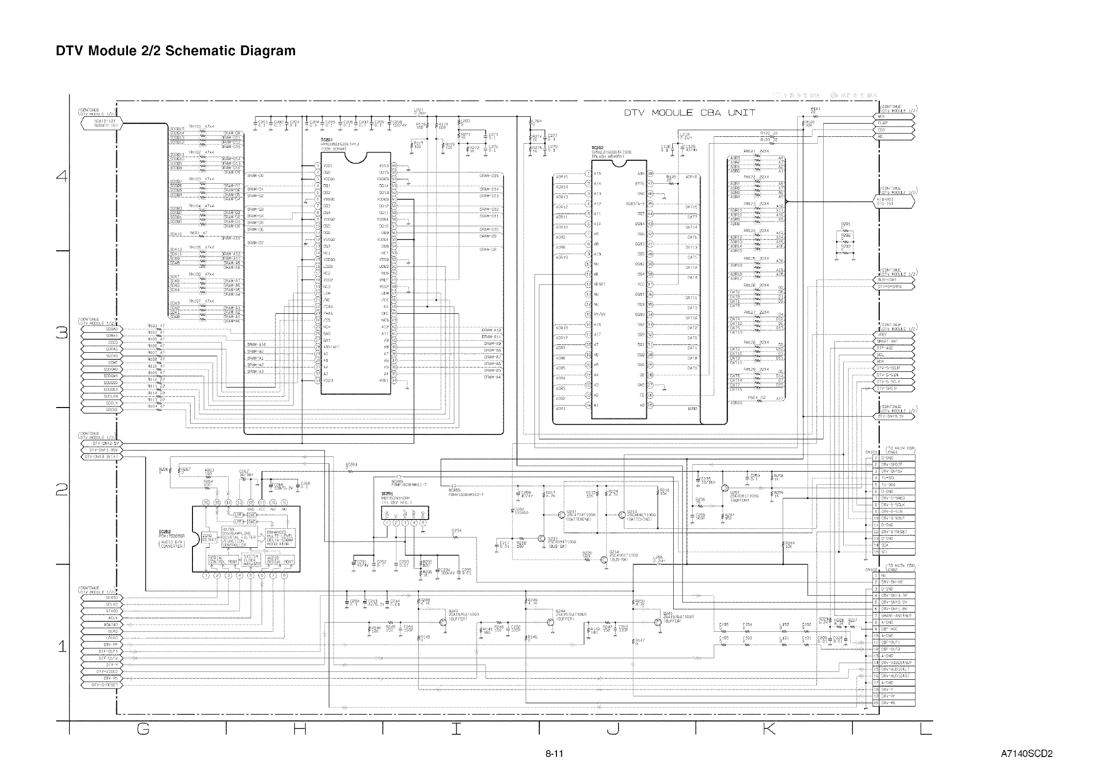
DTV Module 2/2 Schematic Diagram
Z
£
2
8-11 A7140SCD2
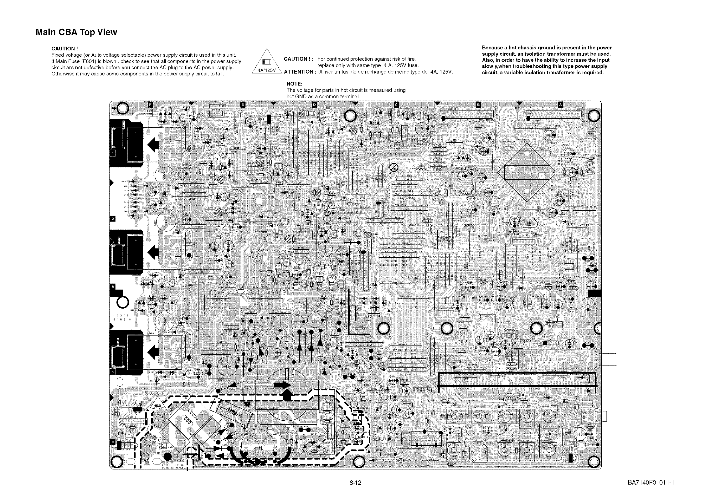
Main CBA Top View
CAUTION !
Fixed voltage (or Auto voltage selectable) power supply circuit is used in this unit.
If Main Fuse (F601) is blown, check to see that all components in the power supply
circuit are not defective before you connect the AC plug to the AC power supply.
Otherwise it may cause some components in the power supply circuit to fail.
_CAUTION ! For continued risk of
protection against fire,
replace only with same type 4 A, 125V fuse.
/_JL_v \ ATTENTION : Utiliser un fusible de rechange de m_me type de 4A, 125V.
NOTE:
The voltage for parts in hot circuit is measured using
hot GND as a common terminal.
Because a hot chassis ground is present in the power
supply circuit, an isolation transformer must be used.
Also, in order to have the ability to increase the input
slowly,when troubleshooting this type power supply
circuit, a variable isolation transformer is required.
8-12 BA7140F01011-1
Main CBA Bottom View
CAUTION !
Fixed voltage (or Auto voltage selectable) power supply circuit is used in this unit.
If Main Fuse (F601) is blown, check to see that all components in the power supply
circuit are not defective before you connect the AC plug to the AC power supply.
Otherwise it may cause some components in the power supply circuit to fail.
CAUTION ! :For continued protection against risk of fire,
replace only with same type 4 A, 125V fuse.
ATTENTION : Utiliser un fusible de rechange de m_me type de 4A, 125V.
NOTE:
The voltage for parts in hot circuit is measured using
hot GND as a common terminal.
Because a hot chassis ground is present in the power
supply circuit, an isolation transformer must be used.
Also, in order to have the ability to increase the input
slowly, when troubleshooting this type power supply
circuit, a variable isolation transformer is required.
I|vivl_
PIN 75 OF
I01202
I|vivl_1
PIN 76 OF
I01202
I|vivl_J
PIN 56 OF
I01202
I |vlvl_
PIN 57 OF
I01202
I |vlvl_
PIN 66 OF
I01202
PIN 71 OF
I01202
I|vlvJ_
10801
8-13 BA7140F01011-1
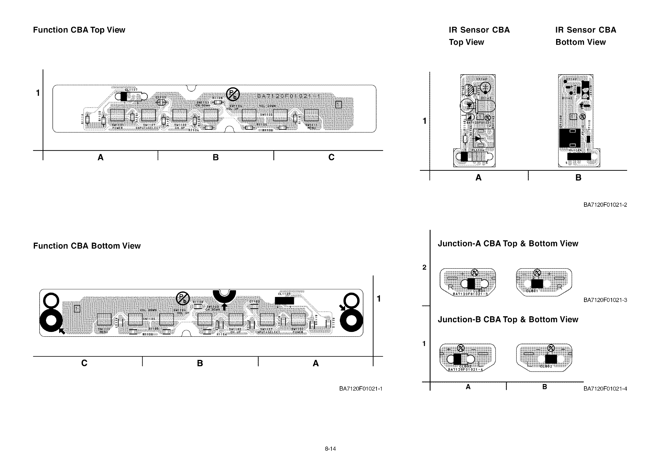
Function CBA Top View IR Sensor CBA
Top View
IR Sensor CBA
Bottom View
A B C
AIa
BA7120F01021-2
Function CBA Bottom View
CB A
BA7120F01021-1
Junction-A CBA Top & Bottom View
Junction-B CBA Top & Bottom View
A I B
BA7120F01021-3
BA7120F01021-4
8-14
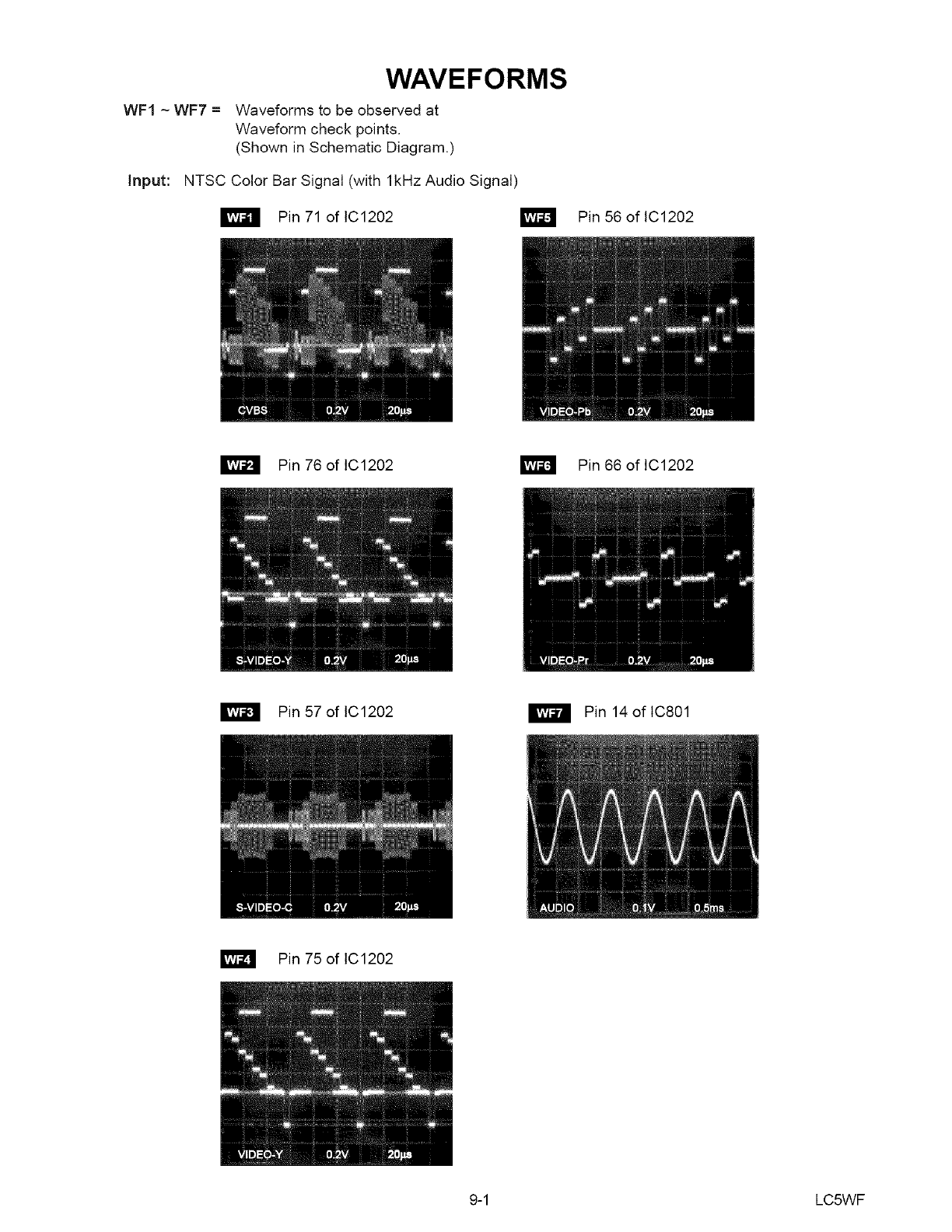
WF1~WF7=
input:
WAVEFORMS
Waveforms to be observed at
Waveform check points.
(Shown in Schematic Diagram,)
NTSC Color Bar Signal (with lkHz Audio Signal)
Pin 71 of tC1202 Pin 56 of IC1202
Pin 76 of tC1202 Pin 66 of tC1202
Pin 57 of IC1202 Pin 14 of IC801
Pin 75 of IC1202
9-1 LC5WF
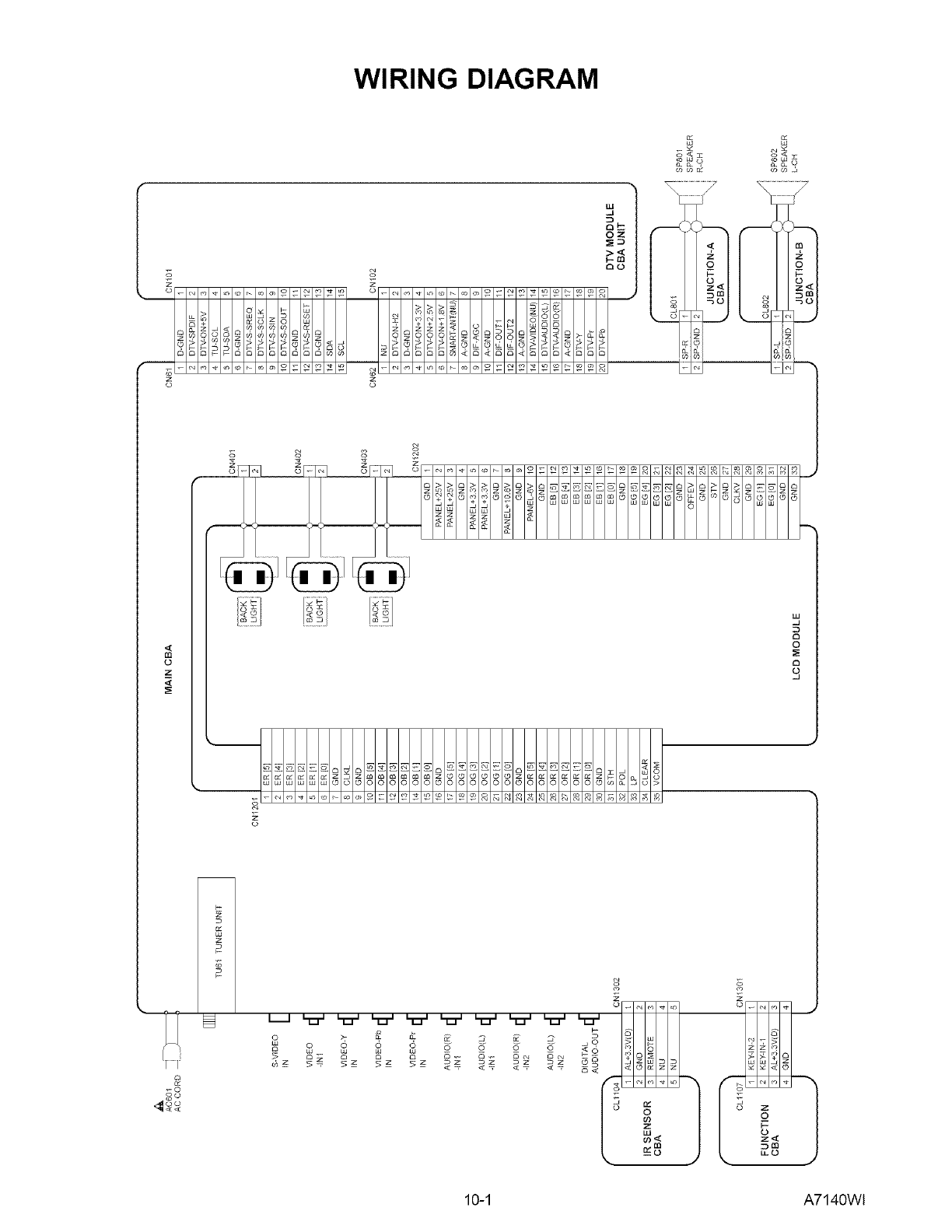
WIRING DIAGRAM
Z
g
121
0
121
g
_0
oo
O0
10-1 A7140WI
IC PIN FUNCTION DESCRIPTIONS
IC1202 (LCD Drive /LCD Signal
Process /TV Micro Controller)
Pin Signal Name Function
No.
1 VDD+3.3V +3.3V VDD
2 VDD+3.3V +3.3V VDD
3 KEY-IN-1 Key Input 1
4 KEY-IN-2 Key Input 2
5 AFT-IN AFTVoltage Input
6 PROTECT-1 Power Supply Protection 1
7 PROTECT-2 Power Supply Protection 2
8 PROTECT-4 Power Supply Protection 4
9 ADIN6 Reference Terminal
10 VSS GND
11 NU Not Used
12 NU Not Used
13 NU Not Used
14 NU Not Used
15 DTV-S-SOUT DTV Serial Data Out
16 DTV-S-SIN DTV Serial Data In
17 DTV-S-SREQ DTV Serial Request
18 IF-MUTE IF Mute Signal Output
19 VCOM VCOM
BACKLIGHT-
20 ADJ Inverter Control Signal Output
21 VDD+3.3V +3.3V VDD
22 DTV-ON-H2 DTV On Signal 2 at High
23 VOLUME Volume Control Signal Output
24 VDD+I.2V +1.2V VDD
25 VDD+I.2V +1.2V VDD
26 VGH-H VGH Signal at High
27 P-ON-H Power On Signal at High
28 REMOTE Remote Control Signal Input
29 BUS-OPEN Chip select
30 SCL Serial Clock
31 SDA Serial Data
32 NU Not Used
33 NU Not Used
34 NU Not Used
35 NU Not Used
36 NU Not Used
37 XIN Crystal Oscillation Input
(27MHz)
Pin Signal Name Function
No.
38 XOUT Crystal Oscillation Output
(27MHz)
39 VSS GND
40 VSS GND
41 VSS GND
42 VDD+3.3V +3.3V VDD
43 VDD+3.3V +3.3V VDD
44 FSC Clock Output
45 MPSEL MP Select
46 TEST GND
47 S-SW Detecting S-VIDEO Jack
Connection
48 AUDIO-MUTE Audio Mute Signal Output
49 INPUT-0 Input Select 0 Signal Output
50 INPUT-1 Input Select 1 Signal Output
51 INPUT-2 Input Select 2 Signal Output
52 NU Not Used
53 NU Not Used
54 DTV-Pb DTV Pb Signal Input
55 NU Not Used
56 VIDEO-Pb Component Video Pb Signal
Input
57 S-VIDEO-C Chrominance Signal Input
58 AVDDB +3.3V VDD
59 AVSSB GND
60 SVSS GND
61 NU Not Used
62 NU Not Used
63 NU Not Used
64 DTV-Pr DTV Pr Signal Input
65 NU Not Used
66 VIDEO-Pr Component Video Pr Signal
Input
67 RF-CVBS Composite Video Signal Input
68 AVDDC +3.3V VDD
69 AVSSC GND
70 NU Not Used
71 VIDEO-IN1 Composite Video Signal Input
72 NU Not Used
73 DTV-Y DTV Y Signal Input
74 NU Not Used
75 VIDEO-Y Component Video Y Signal
Input
11-1 A71 40PIN
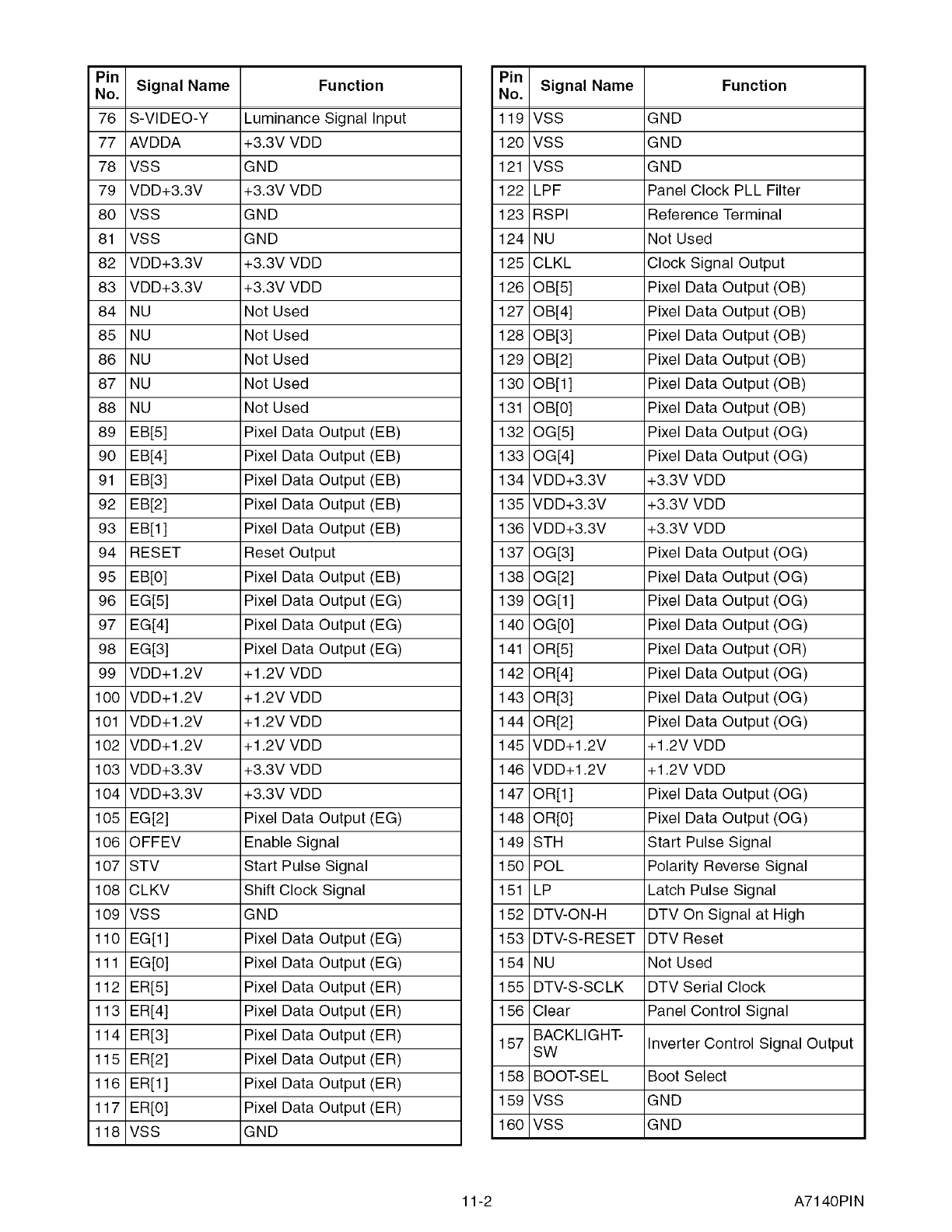
Pin Signal Name Function
No.
76 S-VIDEO-Y Luminance Signal Input
77 AVDDA +3.3V VDD
78 VSS GND
79 VDD+3.3V +3.3V VDD
80 VSS GND
81 VSS GND
82 VDD+3.3V +3.3V VDD
83 VDD+3.3V +3.3V VDD
84 NU Not Used
85 NU Not Used
86 NU Not Used
87 NU Not Used
88 NU Not Used
89 EB[5] Pixel Data Output (EB)
90 EB[4] Pixel Data Output (EB)
91 EB[3] Pixel Data Output (EB)
92 EB[2] Pixel Data Output (EB)
93 EB[1] Pixel Data Output (EB)
94 RESET Reset Output
95 EB[0] Pixel Data Output (EB)
96 EG[5] Pixel Data Output (EG)
97 EG[4] Pixel Data Output (EG)
98 EG[3] Pixel Data Output (EG)
99 VDD+I.2V +1.2V VDD
100 VDD+1.2V +1.2V VDD
101 VDD+I.2V +1.2V VDD
102 VDD+1.2V +1.2V VDD
103 VDD+3.3V +3.3V VDD
104 VDD+3.3V +3.3V VDD
105 EG[2] Pixel Data Output (EG)
106 OFFEV Enable Signal
107 STV Start Pulse Signal
108 CLKV Shift Clock Signal
109 VSS GND
110 EG[1] Pixel Data Output (EG)
111 EG[0] Pixel Data Output (EG)
112 ER[5] Pixel Data Output (ER)
113 ER[4] Pixel Data Output (ER)
114 ER[3] Pixel Data Output (ER)
115 ER[2] Pixel Data Output (ER)
116 ER[1] Pixel Data Output (ER)
117 ER[0] Pixel Data Output (ER)
118 VSS GND
Pin Signal Name Function
No.
119 VSS GND
120 VSS GND
121 VSS GND
122 LPF Panel Clock PLL Filter
123 RSPI Reference Terminal
124 NU Not Used
125 CLKL Clock Signal Output
126 OB[5] Pixel Data Output (OB)
127 OB[4] Pixel Data Output (OB)
128 OB[3] Pixel Data Output (OB)
129 OB[2] Pixel Data Output (OB)
130 OB[1] Pixel Data Output (OB)
131 OB[0] Pixel Data Output (OB)
132 OG[5] Pixel Data Output (OG)
133 OG[4] Pixel Data Output (OG)
134 VDD+3.3V +3.3V VDD
135 VDD+3.3V +3.3V VDD
136 VDD+3.3V +3.3V VDD
137 OG[3] Pixel Data Output (OG)
138 OG[2] Pixel Data Output (OG)
139 OG[1] Pixel Data Output (OG)
140 OG[0] Pixel Data Output (OG)
141 OR[5] Pixel Data Output (OR)
142 OR[4] Pixel Data Output (OG)
143 OR[3] Pixel Data Output (OG)
144 OR[2] Pixel Data Output (OG)
145 VDD+1.2V +1.2V VDD
146 VDD+1.2V +1.2V VDD
147 OR[l] Pixel Data Output (OG)
148 OR[0] Pixel Data Output (OG)
149 STH Start Pulse Signal
150 POL Polarity Reverse Signal
151 LP Latch Pulse Signal
152 DTV-ON-H DTV On Signal at High
153 DTV-S-RESET DTV Reset
154 NU Not Used
155 DTV-S-SCLK DTV Serial Clock
156 Clear Panel Control Signal
BACKLIGHT-
157 SW Inverter Control Signal Output
158 BOOT-SEL Boot Select
159 VSS GND
160 VSS GND
11-2 A71 40PIN
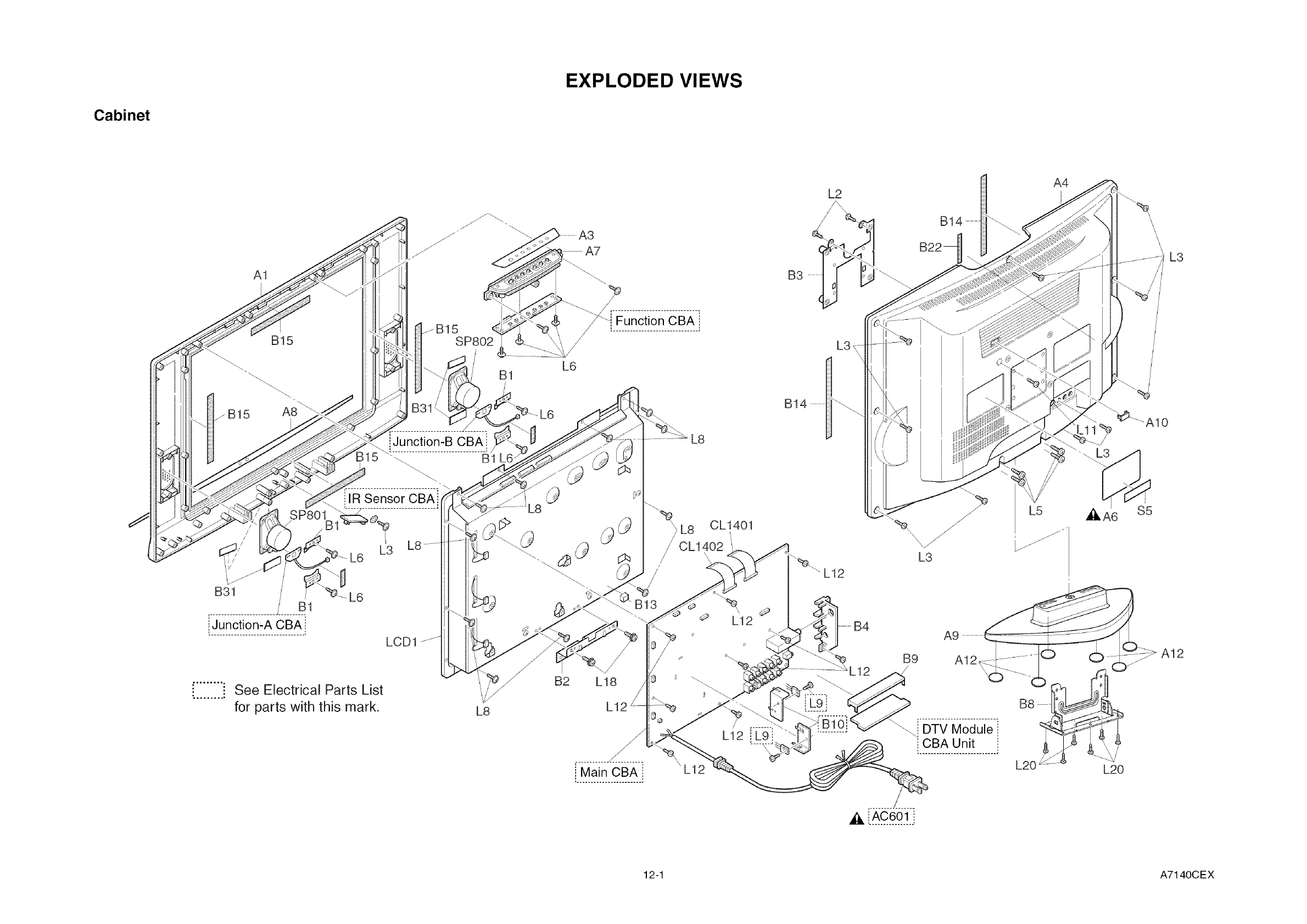
EXPLODED VIEWS
Cabinet
A1
B15 SP802
/
/
iJunction-B CBA ::
"B1
iIR Sensor CBA::
SP801_-O_
L3
L6
LCD1
........". See Electrical Parts List
for parts with this mark. L8
B1
/
/
/
L6
B2
B13
L18
L8
L12
L2
B3
L3
B14 ...........
L12
\ /
L3
A9
B9 A12
/
L5
B8
A4
L20
L3
-A10
$5
A12
12-1 A71 40CEX

Packing
Some Ref. Numbers are
not in sequence.
X1
Tape
$4
\\\
Packing Tape
$2
/
Packing Ta_,.././././ ./"
r'i
\\\
$3
$1
$5
Packing Tape
\ Packing Tape
12-2 A7140PEX
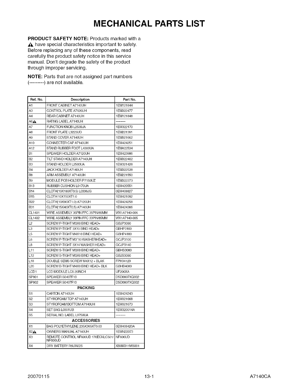
MECHANICAL PARTS LIST
PRODUCT SAFETY NOTE: Products marked with a
,_ have special characteristics important to safety.
Before replacing any of these components, read
carefully the product safety notice in this service
manual. Don't degrade the safety of the product
through improper servicing.
NOTE: Parts that are not assigned part numbers
(......... ) are not available.
Ref. No, Description Part No,
A1 FRONT CABINET A7140UH 1EM121844
A3 CONTROL PLATE A7120UH 1EM322477
A4 REAR CABINET A7140UH 1EM121848
A6_, RATING LABEL A7140UH ........
A7 FUNCTION KNOB L2530JA 1EM322170
A8 FRONT PLATE L3223UD 1EM221391
A9 STAND COVER A7140UH 1EM021662
A10 CONNECTER CAP A7140UH 1EM424251
A12 STAND RUBBER FOOT L4300UA 1EM422534
B1 SPEAKER HOLDER A7120UH 1EM423986
B2 TILT STAND HOLDER A7140UH 1EM322402
B3 STAND HOLDER L2500UA 1EM321428
B4 JACK HOLDER A7140UH 1EM322538
B8 ARM ASSEMBLY A7140UH 1EM221550
B9 MODULE PCB HOLDER P7150UZ 1EM322373
B13 RUBBER CUSHION L0170UA 1EM420551
B14 CLOTH(10X180XT0.5) L0336JG 0EM408827
B15 CLOTH 10X150XT1.0 1EM421092
B22 CLOTH( 10X90XT1.0) A7120U H 1EM424258
B31 CLOTH(15X40XT0.5) A7140UH 1EM424366
CL1401 WIRE ASSEMBLY 35PIN FFC 35PIN/85MM WX1A7140-006
CL1402 WIRE ASSEMBLY 33PIN FFC 33PIN/85MM WX1A7140-005
L2 SCREW P-TIGHT M3X8 BIND HEAD+ GBJP3080
L3 SCREW P-TIGHT 3X10 BIND HEAD+ GBHP3100
L5 SCREW P-TIGHT M4X18 BIND HEAD+ GBHP4180
L6 SCREW P-TIGHT M3"10 WASHERHEAD+ GCJP3100
L8 SCREW P-TIGHT 3X14 WASHER HEAD+ GCJP3140
L11 SCREW S-TIGHT M3X8 BIND HEAD+ GBHS3080
L12 SCREW S-TIGHT M3X8 BIND HEAD+ GBJS3080
L18 DOUBLE SEMS SCREW M4X12 + BLAK FPH34120
L20 SCREW B-TIGHT M4X8 BIND HEAD+ BLK GBHB4080
LCD1 LCD MODULE LC5 20INCH UF200XA
SP801 SPEAKER S0407F10 DSD0807XQ002
SP802 SPEAKER S0407F10 DSD0807XQ002
PACKING
$1 CARTON A7140UH 1EM424243
$2 STYROFOAM TOP A7140UH 1EM021668
$3 STYROFOAM BOTi-OM A7140UH 1EM021673
$4 SET BAG L0301 UB 1EM320014A
$5 SERIAL NO. LABEL L9750UA ........
ACCESSORIES
X1 BAG POLYETHYLENE 235X365XT0.03 0EM408420A
X2_, OWNERS MANUAL A7140UH 1EMN22073
X3 REMOTE CONTROL NF600UD 170ECNLC501/ NF600UD
NF600UD
X4 DRY BATTERY R6UW/2S XBOM311MS001
20070115 13-1 A7140CA
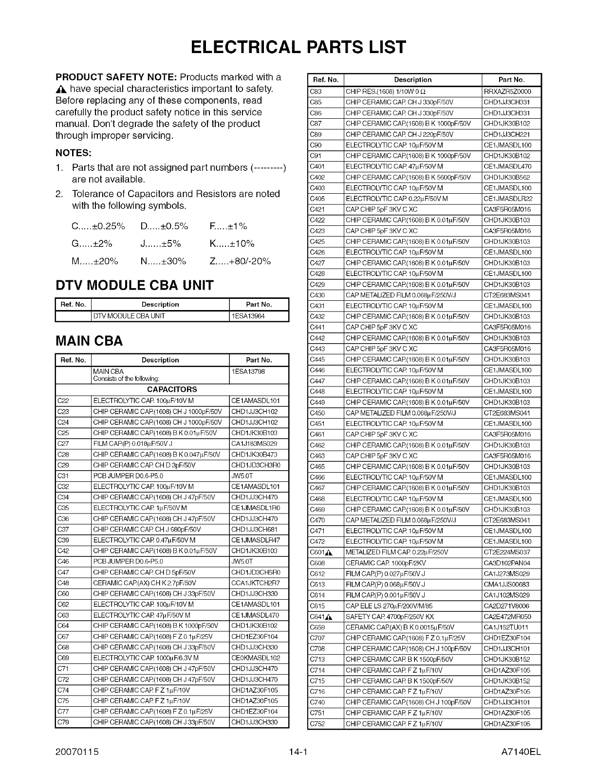
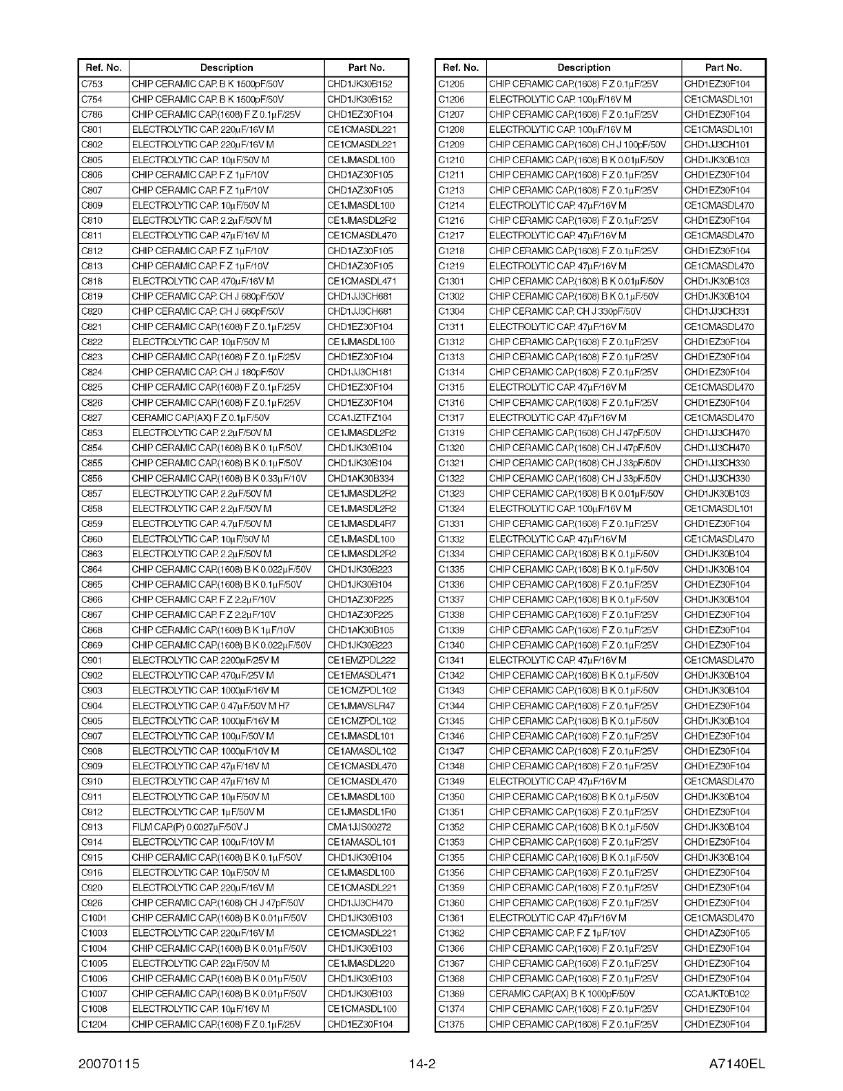
ELECTRICAL PARTS LIST
PRODUCT SAFETY NOTE: Products marked with a
,_ have special characteristics important to safety.
Before replacing any of these components, read
carefully the product safety notice in this service
manual. Don't degrade the safety of the product
through improper servicing.
NOTES:
1. Parts that are not assigned part numbers (......... )
are not available.
2. Tolerance of Capacitors and Resistors are noted
with the following symbols.
C..... +0.25% D.....+0.5% E....+1%
G..... +2% J......+5% K.....+10%
M.....+20% N .....+30% Z..... +80/-20%
DTV MODULE CBA UNIT
Ref. No, Description Part No,
DTV MODULE CBA UN T 1ESA13964
MAIN CBA
Ref, No. Description Part No,
MAIN CBA 1ESA13798
Consists of the following:
CAPACITORS
C22 ELECTROLYTIC CAR 100pF/10V M CE1AMASDL101
C23 CHIP CERAMIC CAR(1608) CH J 1000pF/50V CHD1JJ3CH102
C24 CHIP CERAMIC CAR(1608) CH J 1000pF/50V CHD1JJ3CH102
C25 CHIP CERAMIC CAE(1608) B K 0.01# F/50V CHD1JK30B103
C27 FILM CAR(P) 0.018pF/50V J CA1J183MS029
C28 CHIP CERAMIC CAE(1608) B K 0.047pF/50V CHD1JK30B473
C29 CHIP CERAMIC CAR CH D 3pF/50V CHD1JD3CH3R0
C31 PCB JUMPER D0.6-PE0 JWEOT
C32 ELECTROLYTIC CAR 100pF/10V M CE1AMASDL101
C34 CHIP CERAMIC CAR(1608) CH J 47pF/50V CHD1JJ3CH470
C35 ELECTROLYTIC CAR I#F/50V M CE1JMASDL1R0
C36 CHIP CERAMIC CAR(1608) CH J 47pF/50V CHD1JJ3CH470
C37 CHIP CERAMIC CAR CH J 680pF/50V CHD1JJ3CH681
C39 ELECTROLYTIC CAR 0.47# F/50V M CE1JMASDLR47
C42 CHIP CERAMIC CAE(1608) B K 0.01# F/50V CHD1JK30B103
C46 PCB JUMPER D0.6-PE0 JWEOT
C47 CHIP CERAMIC CAR CH D 5pF/50V CHD1JD3CH5R0
C48 CERAMIC CAR(AX) CH K 2.7pF/50V CCA1JKTCH2R7
C60 CHIP CERAMIC CAR(1608) CH J 33pF/50V CHD1JJ3CH330
C62 ELECTROLYTIC CAR 100pF/10V M CE1AMASDL101
C63 ELECTROLYTIC CAR 47# F/50V M CE1JMASDL470
C64 CHIP CERAMIC CAE(1608) B K 1000pF/50V CHD1JK30B102
C67 CHIP CERAMIC CAR(1608) F Z 0.1# F/25V CHD1EZ30F104
C68 CHIP CERAMIC CAR(1608) CH J 33pF/50V CHD1JJ3CH330
C69 ELECTROLYTIC CAR 1000p F/6.3V M CEOKMASDL102
C71 CHIP CERAMIC CAR(1608) CH J 47pF/50V CHD1JJ3CH470
C72 CHIP CERAMIC CAR(1608) CH J 47pF/50V CHD1JJ3CH470
C74 CHIP CERAMIC CAR FZ lpF/10V CHD1AZ30F105
C75 CHIP CERAMIC CAR FZ lpF/10V CHD1AZ30F105
C77 CHIP CERAMIC CAR(1608) F Z 0.1#LF/25V CHD1EZ30F104
C79 CHIP CERAMIC CAR(1608) CH J 33pF/50V CHD1JJ3CH330
Ref. No. Description Part No.
C83 CHIP RES.(1608) 1/10W 0 _1 RRXAZR5Z0000
C85 CHIP CERAMIC CAR CH J 330pF/50V CHD1JJ3CH331
C86 CHIP CERAMIC CAR CH J 330pF/50V CHD1JJ3CH331
C87 CHIP CERAMIC CAR(1608) B K 1000pF/50V CHD1JK30B102
C89 CHIP CERAMIC CAR CH J 220pF/50V CHD1JJ3CH221
C90 ELECTROLYTIC CAR 10p F/50V M CE1JMASDL100
C91 CHIP CERAMIC CAR(1608) B K 1000pF/50V CHD1JK30B102
C401 ELECTROLYTIC CAR 47p F/50V M CE1JMASDL470
C402 CHIP CERAMIC CAR(1608) B K 5600pF/50V CHD1JK30B562
C403 ELECTROLYTIC CAR 10p F/50V M CE1JMASDL100
C405 ELECTROLYTIC CAR 0.22p F/50V M CE1JMASDLR22
C421 CAP CHIP 8pF 3KV C XC CA3FSR08M016
C422 CHIP CERAMIC CAR(1608) B K 0.01pF/50V CHD1JK30B103
C423 CAP CHIP 5pF 3KV C XC CA3F5R05M016
C425 CHIP CERAMIC CAR(1608) B K 0.01pF/50V CHD1JK30B103
C426 ELECTROLYTIC CAR 10p F/50V M CE1JMASDL100
C427 CHIP CERAMIC CAR(1608) B K 0.01pF/50V CHD1JK30B103
C428 ELECTROLYTIC CAR 10p F/50V M CE1JMASDL100
C429 CHIP CERAMIC CAR(1608) B K 0,01pF/50V CHD1JK30B103
C430 CAP METALIZED FILM 0.068p F/250V/J CT2E683MS041
C431 ELECTROLYTIC CAR 10p F/80V M CE1JMASDL100
C432 CHIP CERAMIC CAR(1608) B K 0.01pF/50V CHD1JK30B103
C441 CAP CHIP 8pF 3KV C XC CA3FSR08M016
C442 CHIP CERAMIC CAR(1608) B K 0.01pF/50V CHD1JK30B103
C443 CAP CHIP 5pF 3KV C XC CA3F5R05M016
C445 CHIP CERAMIC CAR(1608) B K 0.01pF/50V CHD1JK30B103
C446 ELECTROLYTIC CAR 10p F/50V M CE1JMASDL100
C447 CHIP CERAMIC CAR(1608) B K 0.01pF/50V CHD1JK30B103
C448 ELECTROLYTIC CAR 10p F/50V M CE1JMASDL100
C449 CHIP CERAMIC CAR(1608) B K 0.01pF/50V CHD1JK30B103
C450 CAP METALIZED FILM 0.068#tF/250V/J CT2E683MS041
C451 ELECTROLYTIC CAR 10p F/50V M CE1JMASDL100
C461 CAP CHIP 5pF 3KV C XC CA3F5R05M016
C462 CHIP CERAMIC CAR(1608) B K 0.01pF/50V CHD1JK30B103
C463 CAP CHIP 8pF 3KV C XC CA3FSR08M016
C465 CHIP CERAMIC CAR(1608) B K 0.01pF/50V CHD1JK30B103
C466 ELECTROLYTIC CAR 10p F/80V M CE1JMASDL100
C467 CHIP CERAMIC CAR(1608) B K 0.01pF/50V CHD1JK30B103
C468 ELECTROLYTIC CAR 10p F/50V M CE1JMASDL100
0469 CHIP CERAMIC CAR(1608) B K 0.01pF/50V CHD1JK30B103
C470 CAP METALIZED FILM 0.068#F/250V/J CT2E683MS041
C471 ELECTROLYTIC CAR 10p F/50V M CE1JMASDL100
C472 ELECTROLYTIC CAR 10p F/50V M CE1JMASDL100
C601_i& METALIZED FILM CAR 0.22#LF/250V CT2E224MS037
C608 CERAMIC CAR 1000pF/2KV CA3D102PAN04
C612 FILM CAR(P) 0.027p F/50V J CA1J273MS029
C613 FILM CAR(P) 0.068p F/50V J CMA1JJS00683
C614 FILM CAR(P) 0.001pF/50V J CA1J102MS029
C615 CAP ELE LS 270#LF/200V/M/85 CA2D271V8006
C641_i& SAFETY CAR 4700pF/250V KX CA2E472MR050
C659 CERAMIC CAR(AX) B K 0.0015p F/50V CA1J152TU011
C707 CHIP CERAMIC CAR(1608) F Z 0.1p F/25V CHD1EZ30F104
C708 CHIP CERAMIC CAR(1608) CH J 100pF/50V CHD1JJ3CH101
C713 CHIP CERAMIC CAR B K 1500pF/50V CHD1JK30B152
C714 CHIP CERAMIC CAR FZ I#F/10V CHD1AZ30F105
C715 CHIP CERAMIC CAR B K 1500pF/50V CHD1JK30B182
C716 CHIP CERAMIC CAR FZ lpF/10V CHD1AZ30F105
C740 CHIP CERAMIC CAR(1608) CH J 100pF/80V CHD1JJ3CH101
C751 CHIP CERAMIC CAR F Z 1# F/10V CH D1AZ30F105
C752 CHIP CERAMIC CAR F Z I#LF/10V CH D1AZ30F105
20070115 14-1 A7140EL
Ref, No. Description Part No.
C753 CHIP CERAMIC CAR B K 1500pF/50V CHD1JK30B152
C754 CHIP CERAMIC CAR B K 1500pF/50V CHD1JK30B152
C766 CHIP CERAMIC CAR(1608) F Z0.1# F/25V CHD1EZ.30F104
C801 ELECTROLYTIC CAR 220pF/16V M CE1CMASDL221
C802 ELECTROLYTIC CAR 220pF/16V M CE1CMASDL221
C805 ELECTROLYTIC CAR 10#F/50V M CE1JMASDL100
C806 CHIP CERAMIC CAR FZ lpF/10V CHD1AZ30F105
C807 CHIP CERAMIC CAR FZ lpF/10V CHD1AZ30F105
C809 ELECTROLYTIC CAR 10#LF/50VM CE1JMASDL100
C810 ELECTROLYTIC CAR 2.2p F/50V M CE1JMASDL2R2
C811 ELECTROLYTIC CAR 47#LF/16VM CE1CMASDL470
C812 CHIP CERAMIC CAR FZ lpF/10V CHD1AZ30F105
C813 CHIP CERAMIC CAR FZ lpF/10V CHD1AZ30F105
C818 ELECTROLYTIC CAR 470pF/16V M CE1CMASDL471
C819 CHIP CERAMIC CAR CH J 680pF/50V CHD1JJ3CH681
C820 CHIP CERAMIC CAR CH J 680pF/50V CHD1JJ3CH681
C821 CHIP CERAMIC CAR(1608) F Z0.1# F/25V CHD1EZ.30F104
C822 ELECTROLYTIC CAR 10#LF/50VM CE1JMASDL100
C823 CHIP CERAMIC CAR(1608) F Z0.1# F/25V CHD1EZ.30F104
C824 CHIP CERAMIC CAR CH J 180pF/50V CHD1JJ3CH181
C825 CHIP CERAMIC CAR(1608) F Z0.1# F/25V CHD1EZ.30F104
C826 CHIP CERAMIC CAR(1608) F Z0.1# F/25V CHD1EZ.30F104
C827 CERAMIC CAR(AX) F Z0.1# F/50V CCA1JZTFZ104
C853 ELECTROLYTIC CAR 2.2p F/50V M CE1JMASDL2R2
C854 CHIP CERAMIC CAR(1606) B K 0.1#F/50V CHD1JK30B104
C855 CHIP CERAMIC CAR(1606) B K 0.1#F/50V CHD1JK30B104
C856 CHIP CERAMIC CAR(1608) B K 0.33#LF/10V CHD1AK30B334
C857 ELECTROLYTIC CAR 2.2pF/50V M CE1JMASDL2R2
C858 ELECTROLYTIC CAR 2.2pF/50V M CE1JMASDL2R2
C859 ELECTROLYTIC CAR 4.7p F/50V M CE1JMASDL4R7
C860 ELECTROLYTIC CAR 10#F/50V M CE1JMASDL100
C863 ELECTROLYTIC CAR 2.2pF/50V M CE1JMASDL2R2
C864 CHIP CERAMIC CAR(1608) B K 0.022pF/50V CHD1JK30B223
C865 CHIP CERAMIC CAR(1606) B K 0.1#LF/50V CHD1JK30B104
C866 CHIP CERAMIC CAR F Z2.2#F/10V CHD1AZ30F225
C867 CHIP CERAMIC CAR F Z2.2#LF/10V CHD1AZ30F225
C868 CHIP CERAMIC CAR(1608) B K 1#F/10V CHD1AK30B105
C869 CHIP CERAMIC CAR(1608) B K 0.022pF/50V CHD1JK30B223
C901 ELECTROLYTIC CAR 2200p F/25V M CE1 EMZPDL222
C902 ELECTROLYTIC CAR 470p F/25V M CE1 EMASDL471
C903 ELECTROLYTIC CAR 1000p F/16V M CE 1CMZPDL102
C904 ELECTROLYTIC CAR 0.47#F/50V M H7 CE1JMAVSLR47
C905 ELECTROLYTIC CAR 1000p F/16V M CE 1CMZPDL102
C907 ELECTROLYTIC CAR 100pF/50V M CE1JMASDL101
C908 ELECTROLYTIC CAR 1000p F/10V M CE 1AMASDL102
C909 ELECTROLYTIC CAR 47#F/16V M CE1CMASDL470
C910 ELECTROLYTIC CAR 47#LF/16VM CE1CMASDL470
C911 ELECTROLYTIC CAR 10# F/50V M CE1JMASDL100
C912 ELECTROLYTIC CAR I#F/50V M CE1JMASDL1R0
C913 FILM CAR(P) 0.0027#F/50V J CMA1JJS00272
C914 ELECTROLYTIC CAR 100p F/10V M CE 1AMASDL101
C915 CHIP CERAMIC CAR(1608) B K 0.1_LF/50V CHD1JK30B104
C916 ELECTROLYTIC CAR 10#F/50V M CE1JMASDL100
C920 ELECTROLYTIC CAR 220pF/16V M CE1CMASDL221
C926 CHIP CERAMIC CAR(1608) CH J 47pF/50V CHD1JJ3CH470
C1001 CHIP CERAMIC CAR(1608) B K 0.01#LF/50V CHD1JK30B103
C1003 ELECTROLYTIC CAR 220p F/16V M CE1CMASDL221
C1004 CHIP CERAMIC CAR(1608) B K 0.01# F/50V CHD1JK30B103
C1006 ELECTROLYTIC CAR 22# F/50V M CE1JMASDL220
C1006 CHIP CERAMIC CAR(1608) B K 0.01# F/50V CHD1JK30B103
C1007 CHIP CERAMIC CAR(1608) B K 0.01# F/50V CHD1JK30B103
C1008 ELECTROLYTIC CAR 10# F/16V M CE1CMASDL100
C1204 CHIP CERAMIC CAR(1608) F Z 0.1#LF/25V CHD1EZ30F104
Ref. No. Description Part No.
C1205 CHIP CERAMIC CAR(1608) F Z0.1p F/25V CHD1EZ30F104
C1206 ELECTROLYTIC CAR 100# F/16V M CE1CMASDL101
C1207 CHIP CERAMIC CAR(1608) F Z0.1p F/25V CHD1EZ30F104
C1208 ELECTROLYTIC CAR 100# F/16V M CE1CMASDL101
C1209 CHIP CERAMIC CAR(1608) CH J 100pF/50V CHD1JJ3CH101
C1210 CHIP CERAMIC CAR(1608) B K 0.01p F/50V CHD1JK30B103
C1211 CHIP CERAMIC CAR(1608) F Z0.1p F/25V CHD1EZ30F104
C1213 CHIP CERAMIC CAR(1608) F Z0.1p F/25V CHD1EZ30F104
C1214 ELECTROLYTIC CAR 47p F/16V M CE1CMASDL470
C1216 CHIP CERAMIC CAR(1608) F Z0.1p F/25V CHD1EZ30F104
C1217 ELECTROLYTIC CAR 47p F/16V M CE1CMASDL470
C1218 CHIP CERAMIC CAR(1608) F Z0.1p F/25V CHD1EZ30F104
C1219 ELECTROLYTIC CAR 47p F/16V M CE1CMASDL470
C1301 CHIP CERAMIC CAR(1608) B K 0.01p F/50V CHD1JK30B103
C1302 CHIP CERAMIC CAR(1608) B K 0.1p F/50V CHD1JK30B104
C1304 CHIP CERAMIC CAR CH J 330pF/50V CHD1JJ3CH331
C1311 ELECTROLYTIC CAR 47p F/16V M CE1CMASDL470
C1312 CHIPCERAMICCAR(1608) FZO.1pF/25V CHD1EZ30F104
C1313 CHIP CERAMIC CAR(1608) F Z0.1p F/25V CHD1EZ30F104
C1314 CHIPCERAMICCAR(1608) FZO.1pF/25V CHD1EZ30F104
C1315 ELECTROLYTIC CAR 47p F/16V M CE1CMASDL470
C1316 CHIP CERAMIC CAR(1608) F Z0.1p F/25V CHD1EZ30F104
C1317 ELECTROLYTIC CAR 47p F/16V M CE1CMASDL470
C1319 CHIP CERAMIC CAR(1608) CH J 47pF/50V CHD1JJ3CH470
C1320 CHIP CERAMIC CAR(1608) CH J 47pF/50V CHD1JJ3CH470
C1321 CHIP CERAMIC CAR(1608) CH J 33pF/50V CHD1JJ3CH330
C1322 CHIP CERAMIC CAR(1608) CH J 33pF/50V CHD1JJ3CH330
C1323 CHIP CERAMIC CAR(1608) B K 0.01p F/50V CHD1JK30B103
C1324 ELECTROLYTIC CAR 100#LF/16VM CE1CMASDL101
C1331 CHIP CERAMIC CAR(1608) F Z0.1p F/25V CHD1EZ30F104
C1332 ELECTROLYTIC CAR 47p F/16V M CE1CMASDL470
C1334 CHIP CERAMIC CAR(1608) B K 0.1p F/50V CHD1JK30B104
C1335 CHIP CERAMIC CAR(1608) B K 0.1p F/50V CHD1JK30B104
C1336 CHIPCERAMICCAR(1608) FZO.1pF/25V CHD1EZ30F104
C1337 CHIP CERAMIC CAR(1608) B K 0.1p F/50V CHD1JK30B104
C1338 CHIPCERAMICCAR(1608) FZO.1pF/25V CHD1EZ30F104
C1339 CHIP CERAMIC CAR(1608) F Z0.1p F/25V CHD1EZ30F104
C1340 CHIP CERAMIC CAR(1608) F Z0.1p F/25V CHD1EZ30F104
C1341 ELECTROLYTIC CAR 47p F/16V M CE1CMASDL470
C1342 CHIP CERAMIC CAR(1608) B K 0.1p F/50V CHD1JK30B104
C1343 CHIP CERAMIC CAR(1608) B K 0.1p F/50V CHD1JK30B104
C1344 CHIP CERAMIC CAR(1608) F Z0.1p F/25V CHD1EZ30F104
C1345 CHIP CERAMIC CAR(1608) B K 0.1p F/50V CHD1JK30B104
C1346 CHIP CERAMIC CAR(1608) F Z0.1p F/25V CHD1EZ30F104
C1347 CHIPCERAMICCAR(1608) FZO.1pF/25V CHD1EZ30F104
C1348 CHIP CERAMIC CAR(1608) F Z0.1p F/25V CHD1EZ30F104
C1349 ELECTROLYTIC CAR 47p F/16V M CE1CMASDL470
C1350 CHIP CERAMIC CAR(1608) B K 0.1p F/50V CHD1JK30B104
C1351 CHIP CERAMIC CAR(1608) F Z0.1p F/25V CHD1EZ30F104
C1352 CHIP CERAMIC CAR(1608) B K 0.1p F/50V CHD1JK30B104
C1353 CHIP CERAMIC CAR(1608) F Z0.1p F/25V CHD1EZ30F104
C1355 CHIP CERAMIC CAR(1608) B K 0.1p F/50V CHD1JK30B104
C1356 CHIP CERAMIC CAR(1608) F Z0.1p F/25V CHD1EZ30F104
C1359 CHIPCERAMICCAR(1608) FZO.1pF/25V CHD1EZ30F104
C1360 CHIP CERAMIC CAR(1608) F Z0.1p F/25V CHD1EZ30F104
C1361 ELECTROLYTIC CAR 47p F/16V M CE1CMASDL470
C1362 CHIP CERAMIC CAR FZ I#F/10V CHD1AZ30F105
C1366 CHIP CERAMIC CAR(1608) F Z0.1p F/25V CHD1EZ30F104
C1367 CHIP CERAMIC CAR(1608) F Z0.1p F/25V CHD1EZ30F104
C1368 CHIP CERAMIC CAR(1608) F Z0.1p F/25V CHD1EZ30F104
C1369 CERAMIC CAR(AX) B K 1000pF/50V CCA1JKTOB102
C1374 CHIP CERAMIC CAR(1608) F Z0.1p F/25V CHD1EZ30F104
C1375 CHIPCERAMICCAR(1608) FZO.1pF/25V CHD1EZ30F104
20070115 14-2 A7140EL
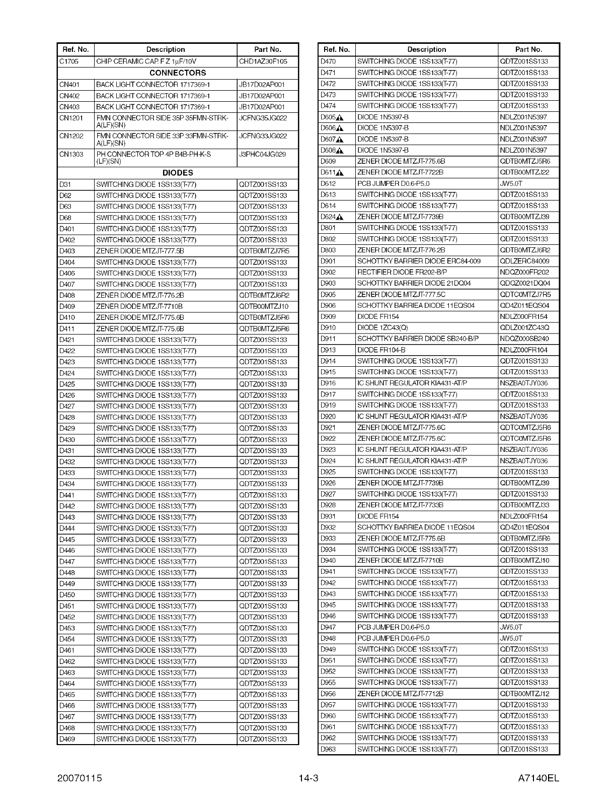
Ref, No, Description Part No,
C1705 CH P CERAM C CAR FZ lpF/10V CHD1AZ30F105
CONNECTORS
CN4Ol BACK LIGHT CONNECTOR 1717369-1 JB17DO2APOO1
CN4O2 BACK LIGHT CONNECTOR 1717369-1 JB17DO2APOO1
CN4O3 BACK LIGHT CONNECTOR 1717369-1 JB17DO2APOO1
CN1201 FMN CONNECTOR SIDE 35P 35FMN_STRK- JCFNG35JGO22
A(LF)(SN)
CN1202 FMN CONNECTOR SIDE 33P 33FMN-STRK- JCFNG33JGO22
A(LF)(SN)
CN1303 PH CONNECTOR TOP 4P B4B-PH-K-S J3PHC04JGO29
(LF)(SN)
DIODES
D31 SWITCHING DIODE 1SS133(T-77) QDTZOO1SS133
D62 SWITCHING DIODE 1SS133(T-77) QDTZOO1SS133
D63 SWITCHING DIODE 1SS133(T-77) QDTZOO1SS133
D68 SWITCHING DIODE 1SS133(T-77) QDTZOOl SS133
D401 SWITCHING DIODE 1SS133(T-77) QDTZOO1SS133
D402 SWITCHING DIODE 1SS133(T-77) QDTZOO1SS133
D403 ZENER DIODE MTZJT-777,5B QDTBOMTZJ7R5
D404 SWITCHING DIODE 1SS133(T-77) QDTZOO1SS133
D406 SWITCHING DIODE 1SS133(T-77) QDTZOO1SS133
D407 SWITCHING DIODE 1SS133(T-77) QDTZOO1SS133
D408 ZENER DIODE MTZJT-776.2B QDTBOMTZJ6R2
D409 ZENER DIODE MTZJT-771OB QDTBOOMTZJ10
D410 ZENER DIODE MTZJT-775.6B QDTBOMTZJ6R6
D411 ZENER DIODE MTZJT-775.6B QDTBOMTZJSR6
D421 SWITCHING DIODE 1SS133(T-77) QDTZOO1SS133
D422 SWITCHING DIODE 1SS133(T-77) QDTZOO1SS133
D423 SWITCHING DIODE 1SS133(T-77) QDTZOO1SS133
D424 SWITCHING DIODE 1SS133(T-77) QDTZOO1SS133
D425 SWITCHING DIODE 1SS133(T-77) QDTZOO1SS133
D426 SWITCHING DIODE 1SS133(T-77) QDTZOO1SS133
D427 SWITCHING DIODE 1SS133(T-77) QDTZOO1SS133
D428 SWITCHING DIODE 1SS133(T-77) QDTZOO1SS133
D429 SWITCHING DIODE 1SS133(T-77) QDTZOO1SS133
D430 SWITCHING DIODE 1SS133(T-77) QDTZOO1SS133
D431 SWITCHING DIODE 1SS133(T-77) QDTZOO1SS133
D432 SWITCHING DIODE 1SS133(T-77) QDTZOO1SS133
D433 SWITCHING DIODE 1SS133(T-77) QDTZOO1SS133
D434 SWITCHING DIODE 1SS133(T-77) QDTZOO1SS133
D441 SWITCHING DIODE 1SS133(T-77) QDTZOO1SS133
D442 SWITCHING DIODE 1SS133(T-77) QDTZOO1SS133
D443 SWITCHING DIODE 1SS133(T-77) QDTZOO1SS133
D444 SWITCHING DIODE 1SS133(T-77) QDTZOO1SS133
D445 SWITCHING DIODE 1SS133(T-77) QDTZOO1SS133
D446 SWITCHING DIODE 1SS133(T-77) QDTZOO1SS133
D447 SWITCHING DIODE 1SS133(T-77) QDTZOO1SS133
D448 SWITCHING DIODE 1SS133(T-77) QDTZOO1SS133
D449 SWITCHING DIODE 1SS133(T-77) QDTZOO1SS133
D450 SWITCHING DIODE 1SS133(T-77) QDTZOO1SS133
D451 SWITCHING DIODE 1SS133(T-77) QDTZOO1SS133
D452 SWITCHING DIODE 1SS133(T-77) QDTZOO1SS133
D453 SWITCHING DIODE 1SS133(T-77) QDTZOO1SS133
D454 SWITCHING DIODE 1SS133(T-77) QDTZOO1SS133
D461 SWITCHING DIODE 1SS133(T-77) QDTZOO1SS133
D462 SWITCHING DIODE 1SS133(T-77) QDTZOO1SS133
D463 SWITCHING DIODE 1SS133(T-77) QDTZOO1SS133
D464 SWITCHING DIODE 1SS133(T-77) QDTZOO1SS133
D465 SWITCHING DIODE 1SS133(T-77) QDTZOO1SS133
D466 SWITCHING DIODE 1SS133(T-77) QDTZOO1SS133
D467 SWITCHING DIODE 1SS133(T-77) QDTZOO1SS133
D468 SWITCHING DIODE 1SS133(T-77) QDTZOO1SS133
D469 SWITCHING DIODE 1SS133(T-77) QDTZOO1SS133
Ref. No. Description Part No.
D470 SWITCHING DIODE 1SS133(T-77) QDTZ001SS133
D471 SWITCHING DIODE 1SS133(T-77) QDTZOO1SS133
D472 SWITCHING DIODE 1SS133(T-77) QDTZOO1SS133
D473 SWITCHING DIODE 1SS133(T-77) QDTZOO1SS133
D474 SWITCHING DIODE 1SS133(T-77) QDTZOO1SS133
D605_ DIODE 1N5397-B NDI 7001N5397
D606_, DIODE 1N5397-B NDI 7001N5397
D6O7_i& DIODE 1N5397-B NDI 7001N5397
D6O8_i& DIODE 1N6397-B NDI 7001N5397
D609 ZENER DIODE MTZJT-775.6B QDTBOMTZJ5R6
D61 l_i& ZENER DIODE MTZJT-7722B QDTBOOMTZJ22
D612 PCB JUMPER DO.6-P5.O JW5.OT
D613 SWITCHING DIODE 1SS133(T-77) QDTZOO1SS133
D614 SWITCHING DIODE 1SS133(T-77) QDTZOO1SS133
D624_, ZENER DIODE MTZJT-7739B QDTBOOMTZJ39
D801 SWITCHING DIODE 1SS133(T-77) QDTZOO1SS133
D802 SWITCHING DIODE 1SS133(T-77) QDTZOO1SS133
D803 ZENER DIODE MTZJT-776.2B QDTBOMTZJ6R2
Dgo1 SCHOTTKY BARRIER DIODE ERC84-009 QDLZERC84009
D902 RECTIFIER DIODE FR202-B/P NDQZOOOFR2O2
D903 SCHOTTKY BARRIER DIODE 21 DQO4 QDQZOO21DQO4
D905 ZENER DIODE MTZJT-777.5C QDTCOMTZJ7R5
D906 SCHOTTKY BARRIEA DIODE 11EQS04 QD4ZOl 1EQSO4
D909 DIODE FR154 NDLZOOOFR154
D910 DIODE 1ZC43(Q) QDI 7001ZC43Q
D911 SCHOTTKY BARRIER DIODE SB24O-B/P NDQZOOOSB240
D913 DIODE FR104-B NDI 7OOOFR1O4
D914 SWITCHING DIODE 1SS133(T-77) QDTZOO1SS133
D915 SWITCHING DIODE 1SS133(T-77) QDTZOO1SS133
D916 IC SHUNT REGULATOR KIA431-AT/P NSZBAOTJYO36
D917 SWITCHING DIODE 1SS133(T-77) QDTZOO1SS133
D919 SWITCHING DIODE 1SS133(T-77) QDTZOO1SS133
D920 IC SHUNT REGULATOR KIA431-AT/P NSZBAOTJYO36
D921 ZENER DIODE MTZJT-775.6C QDTCOMTZJSR6
D922 ZENER DIODE MTZJT-775.6C QDTCOMTZJSR6
D923 IC SHUNT REGULATOR KIA431-AT/P NSZBAOTJYO36
D924 IC SHUNT REGULATOR KIA431-AT/P NSZBAOTJYO36
D925 SWITCHING DIODE 1SS133(T-77) QDTZOO1SS133
D926 ZENER DIODE MTZJT-7739B QDTBOOMTZJ39
D927 SWITCHING DIODE 1SS133(T-77) QDTZOO1SS133
D928 ZENER DIODE MTZJT-7733B QDTBOOMTZJ33
D931 DIODE FR154 NDI 7000FR164
D932 SCHOTTKY BARRIEA DIODE 11EQS04 QD4ZOl 1EQSO4
D933 ZENER DIODE MTZJT-775.6B QDTBOMTZJ5R6
D934 SWITCHING DIODE 1SS133(T-77) QDTZOO1SS133
D940 ZENER DIODE MTZJT-771OB QDTBOOMTZJ1O
D941 SWITCHING DIODE 1SS133(T-77) QDTZOO1SS133
D942 SWITCHING DIODE 1SS133(T-77) QDTZOO1SS133
D943 SWITCHING DIODE 1SS133(T-77) QDTZOO1SS133
D945 SWITCHING DIODE 1SS133(T-77) QDTZOO1SS133
D946 SWITCHING DIODE 1SS133(T-77) QDTZOO1SS133
D947 PCB JUMPER DO.6-P5.O JW5.OT
D948 PCB JUMPER DO.6-P5.O JW5.OT
D949 SWITCHING DIODE 1SS133(T-77) QDTZOO1SS133
D951 SWITCHING DIODE 1SS133(T-77) QDTZOO1SS133
D952 SWITCHING DIODE 1SS133(T-77) QDTZOO1SS133
D955 SWITCHING DIODE 1SS133(T-77) QDTZOO1SS133
D956 ZENER DIODE MTZJT-7712B QDTBOOMTZJ12
D957 SWITCHING DIODE 1SS133(T-77) QDTZOO1SS133
D960 SWITCHING DIODE 1SS133(T-77) QDTZOO1SS133
D961 SWITCHING DIODE 1SS133(T-77) QDTZOO1SS133
D962 SWITCHING DIODE 1SS133(T-77) QDTZOO1SS133
D963 SWITCHING DIODE 1SS133(T-77) QDTZOO1SS133
20070115 14-3 A7140EL
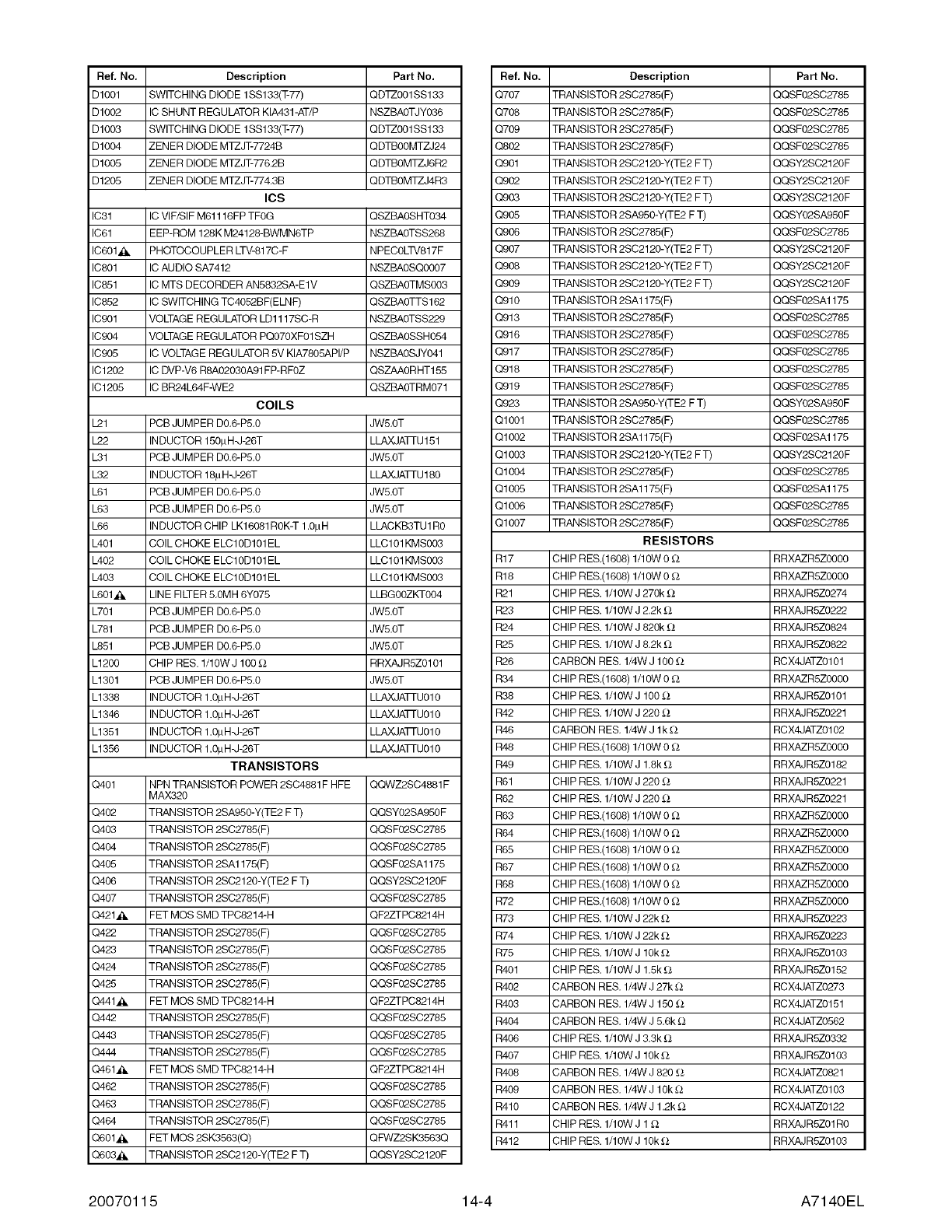
Ref, No. Description Part No.
D1001 SWITCHING DIODE 1SS133(T-77) QDTZ001SS133
D1002 IC SHUNT REGULATOR KIA431-AT/P NSZBAOTJY036
D1003 SWITCHING DIODE 1SS133(T-77) QDTZ001SS133
D1004 ZENER DIODE MTZJT-7724B QDTB00MTZJ24
D1005 ZENER DIODE MTZJT-7762B QDTBOMTZJ6R2
D1205 ZENER DIODE MTZJT-774,3B QDTBOMTZJ4R3
ICS
IC31 IC VlF/SIF M61116FP TFOG QSZBAOSHT034
IC61 EEP-ROM 128K M24128-BWMN6TP NSZBAOTSS268
IC601_ PHOTOCOUPLER LTV-817C-F NPECOLTV817F
IC801 IC AUDIO SA7412 NSZBAOSQ0007
IC851 IC MTS DECORDER AN5832SA-E1V QSZBAOTMS003
IC852 IC SWITCHING TC4052BF(ELNF) QSZBAOTTS162
IC901 VOLTAGE REGULATOR LD1117SC-R NSZBAOTSS229
IC904 VOLTAGE REGULATOR PQ070XF01SZH QSZBAOSSH054
IC905 IC VOLTAGE REGULATOR 5V KIA7805API/P NSZBAOSJY041
IC1202 IC DVP-V6 R8A02030A91FP-RFOZ QSZAAORHT155
IC1205 IC BR24L64F-WE2 QSZBAOTRM071
COILS
L21 PCB JUMPER D0,6-P5,0 JW5,0T
L22 INDUCTOR 150pH_I-26T LLAXJATi-U 151
L31 PCB JUMPER D0,6-P5,0 JWS,0T
L32 INDUCTOR 18p H_I-26T LLAXJATi-U 180
L61 PCB JUMPER D0,6-P5,0 JW5,0T
L63 PCB JUMPER D0.6-P5.0 JW5,0T
L66 INDUCTOR CHIP LK16081ROK-T 1.0pH LLACKB3TU1 R0
L401 COIL CHOKE ELC10D101 EL LLC101 KMS003
L402 COIL CHOKE ELC10D101 EL LLC101KMS003
L403 COIL CHOKE ELC10D101 EL LLC101 KMS003
L601_, LINE FILTER 5,0MH 6Y075 LLBG00ZKT004
L701 PCB JUMPER D0,6-P5,0 JWS,0T
L781 PCB JUMPER D0,6-P5,0 JWS,0T
L851 PCB JUMPER D0,6-PS,0 JW5,0T
L1200 CHIP RES. 1/10W J 100_ RRXAJR5Z0101
L1301 PCB JUMPER D0,6-PS,0 JW5,0T
L1338 INDUCTOR 1.0p H_J-26T LLAXJATi-U010
L1346 INDUCTOR 1.0p H_J-26T LLAXJATi-U010
L1351 INDUCTOR 1.0p H_J-26T LLAXJATi-U010
L1356 INDUCTOR 1.0p H_J-26T LLAXJATi-U010
TRANSISTORS
Q401 NPN TRANSISTOR POWER 2SC4881F HFE QQWZ2SC4881F
MAX320
Q402 TRANSISTOR 2SA950-Y(TE2 F T) QQSY02SA950F
Q403 TRANSISTOR 2SC2785(F) QQSF02SC2785
Q404 TRANSISTOR 2SC2785(F) QQSF02SC2785
Q405 TRANSISTOR 2SA1175(F) QQSF02SA1175
Q406 TRANSISTOR 2SC2120-Y(TE2 F T) QQSY2SC2120F
Q407 TRANSISTOR 2SC2785(F) QQSF02SC2785
Q421_, FET MOS SMD TPC8214-H QF2ZTPC8214H
Q422 TRANSISTOR 2SC2785(F) QQSF02SC2785
Q423 TRANSISTOR 2SC2785(F) QQSF02SC2785
Q424 TRANSISTOR 2SC2785(F) QQSF02SC2785
Q425 TRANSISTOR 2SC2785(F) QQSF02SC2785
Q441_, FET MOS SMD TPC8214-H QF2ZTPC8214H
Q442 TRANSISTOR 2SC2785(F) QQSF02SC2785
Q443 TRANSISTOR 2SC2785(F) QQSF02SC2785
Q444 TRANSISTOR 2SC2785(F) QQSF02SC2785
Q461_, FET MOS SMD TPC8214-H QF2ZTPC8214H
Q462 TRANSISTOR 2SC2785(F) QQSF02SC2785
Q463 TRANSISTOR 2SC2785(F) QQSF02SC2785
Q464 TRANSISTOR 2SC2785(F) QQSF02SC2785
Q601_ FET MOS 2SK3563(Q) QFWZ2SK3563Q
Q603_ TRANSISTOR 2SC2120-Y(TE2 F T) QQSY2SC2120F
Ref. No. Description Part No.
Q707 TRANSISTOR 2SC2785(F) QQSF02SC2785
Q708 TRANSISTOR 2SC2785(F) QQSF02SC2785
Q709 TRANSISTOR 2SC2785(F) QQSF02SC2785
Q802 TRANSISTOR 2SC2785(F) QQSF02SC2785
(3901 TRANSISTOR 2SC2120-Y(TE2 FT) QQSY2SC2120F
Q902 TRANSISTOR 2SC2120-Y(TE2 FT) QQSY2SC2120F
(3903 TRANSISTOR 2SC2120-Y(TE2 FT) QQSY2SC2120F
Q905 TRANSISTOR 2SA950-Y(TE2 F T) QQSY02SA950F
Q906 TRANSISTOR 2SC2785(F) QQSF02SC2785
Q907 TRANSISTOR 2SC2120-Y(TE2 FT) QQSY2SC2120F
Q908 TRANSISTOR 2SC2120-Y(TE2 FT) QQSY2SC2120F
(3909 TRANSISTOR 2SC2120-Y(TE2 FT) QQSY2SC2120F
Q910 TRANSISTOR 2SA1175(F) QQSF02SA1175
(3913 TRANSISTOR 2SC2785(F) QQSF02SC2785
Q916 TRANSISTOR 2SC2785(F) QQSF02SC2785
(3917 TRANSISTOR 2SC2785(F) QQSF02SC2785
Q918 TRANSISTOR 2SC2785(F) QQSF02SC2785
Q919 TRANSISTOR 2SC2785(F) QQSF02SC2785
Q923 TRANSISTOR 2SA950-Y(TE2 F T) QQSY02SA950F
Q1001 TRANSISTOR 2SC2785(F) QQSF02SC2785
Q1002 TRANSISTOR 2SA1175(F) QQSF02SA1175
Q1003 TRANSISTOR 2SC2120-Y(TE2 F T) QQSY2SC2120F
Q1004 TRANSISTOR 2SC2785(F) QQSF02SC2785
Q1005 TRANSISTOR 2SA1175(F) QQSF02SA1175
Q1006 TRANSISTOR 2SC2785(F) QQSF02SC2785
Q1007 TRANSISTOR 2SC2785(F) QQSF02SC2785
RESISTORS
R17 CHIP RES,(1608) 1/10W 0 _,t RRXAZR5Z0000
R18 CHIP RES,(1608) 1/10W 0 _,t RRXAZR5Z0000
R21 CHIP RES. 1/10W J 270k _ RRXAJR5Z0274
R23 CHIP RES. 1/10W J 2,2k _ RRXAJR5Z0222
R24 CHIP RES. 1/10W J 820k _ RRXAJR5Z0824
R25 CHIP RES. 1/10W J 82k _ RRXAJRSZ0822
R26 CARBON RES, 1/4W J 100 _ RCX4JATZ0101
R34 CHIP RES,(1608) 1/10W 0 _,t RRXAZR5Z0000
R38 CHIP RES. 1/10W J 100_ RRXAJR5Z0101
R42 CHIP RES. 1/10W J 220 _ RRXAJR5Z0221
R46 CARBON RES. 1/4W J lk _,t RCX4JATZ0102
R48 CHIP RES,(1608) 1/10W 0 _,t RRXAZR5Z0000
R49 CHIP RES. 1/10W J 1,8k _ RRXAJRSZ0182
R61 CHIP RES. 1/10W J 220 _ RRXAJR5Z0221
R62 CHIP RES. 1/10W J 220 _ RRXAJRSZ0221
R63 CHIP RES,(1608) 1/10W 0 _,t RRXAZR5Z0000
R64 CHIP RES,(1608) 1/10W 0 _,t RRXAZR5Z0000
R65 CHIP RES,(1608) 1/10W 0 _,t RRXAZR5Z0000
R67 CHIP RES,(1608) 1/10W 0 _,t RRXAZR5Z0000
R68 CHIP RES,(1608) 1/10W 0 _,t RRXAZR5Z0000
R72 CHIP RES,(1608) 1/10W 0 _,t RRXAZR5Z0000
R73 CHIP RES. 1/10W J 22k _,t RRXAJR5Z0223
R74 CHIP RES. 1/10W J 22k _,t RRXAJR5Z0223
R75 CHIP RES. 1/10W J 1Ok_,t RRXAJRSZ0103
R401 CHIP RES. 1/10W J 1,5k _ RRXAJR5Z0152
R402 CARBON RES, 1/4W J 27k _,t RCX4JATZ0273
R403 CARBON RES, 1/4W J 150 _ RCX4JATZ0181
R404 CARBON RES, 1/4W J 5,6k _ RCX4JATZ0562
R406 CHIP RES. 1/10W J 3,3k _ RRXAJR5Z0332
R407 CHIP RES. 1/10W J 10k£_ RRXAJRSZ0103
R408 CARBON RES. 1/4W J 820 _ RCX4JATZ0821
R409 CARBON RES, 1/4W J 10k _,_ RCX4JATZ0103
R410 CARBON RES. 1/4WJ 1,2k_ RCX4JATZ0122
R411 CHIP RES. 1/10W J 1 _,_ RRXAJRSZ01R0
R412 CHIP RES. 1/10W J 10k_ RRXAJRSZ0103
20070115 14-4 A7140EL
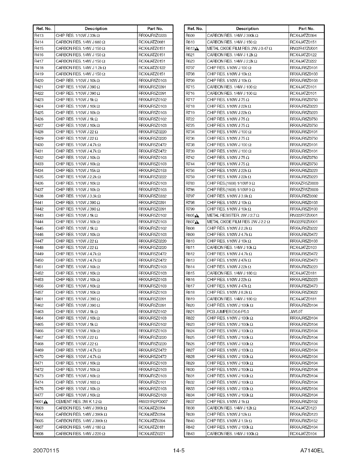
Ref, No. Description Part No.
R413 CHIP RES. 1/10W J 33k _,t RRXAJR5Z0333
R414 CARSON RES. 1/4W J 680 _ RCX4JATZ0681
R415 CARSON RES. 1/4W J 150 _ RCX4JATZ0151
R416 CARSON RES. 1/4W J 150 _ RCX4JATZ0151
R417 CARSON RES. 1/4W J 150 _ RCX4JATZ0151
R418 CARSON RES. 1/4W J 1.2k _,t RCX4JATZ0122
R419 CARSON RES. 1/4W J 150 _ RCX4JATZ0151
R420 CHIP RES. 1/10W J 10k _,t RRXAJR5Z0103
R421 CHIP RES. 1/10W J 390 _ RRXAJR5Z0391
R422 CHIP RES. 1/10W J 390 _ RRXAJR5Z0391
R423 CHIP RES. 1/10W J lk _,t RRXAJR5Z0102
R424 CHIP RES. 1/10W J 10k _,t RRXAJR5Z0103
R425 CHIP RES. 1/10W J 10k _,t RRXAJR5Z0103
R426 CHIP RES. 1/10W J lk _,t RRXAJR5Z0102
R427 CHIP RES. 1/10W J 10k _,t RRXAJR5Z0103
R428 CHIP RES. 1/10W J 22 _ RRXAJR5Z0220
R429 CHIP RES. 1/10W J 22 _ RRXAJR5Z0220
R430 CHIP RES. 1/10W J 4.7k_ RRXAJR5Z0472
R431 CHIP RES. 1/10W J 4.7k _ RRXAJR5Z0472
R432 CHIP RES. 1/10WJ 10k_,t RRXAJR5Z0103
R433 CHIP RES. 1/10W J 10k _,t RRXAJR5Z0103
R434 CHIP RES. 1/10W J 15k _,t RRXAJR5Z0153
R435 CHIP RES. 1/10W J 2.2k _ RRXAJR5Z0222
R436 CHIP RES. 1/10W J 10k _,t RRXAJR5Z0103
R437 CHIP RES. 1/10W J 10k _,t RRXAJR5Z0103
R438 CHIP RES. 1/10W J 3.3k _ RRXAJR5Z0332
R441 CHIP RES. 1/10W J 390 _ RRXAJR5Z0391
R442 CHIP RES. 1/10W J 390 _ RRXAJR5Z0391
R443 CHIP RES. 1/10W J lk _,t RRXAJR5Z0102
R444 CHIP RES. 1/10W J 10k _,t RRXAJR5Z0103
R445 CHIP RES. 1/10W J lk _,t RRXAJR5Z0102
R446 CHIP RES. 1/10W J 10k _,t RRXAJR5Z0103
R447 CHIP RES. 1/10W J 22 _ RRXAJR5Z0220
R448 CHIP RES. 1/10W J 22 _ RRXAJR5Z0220
R449 CHIP RES. 1/10W J 4.7k _ RRXAJR5Z0472
R450 CHIP RES. 1/10W J 4.7k_ RRXAJR5Z0472
R451 CHIP RES. 1/10W J 10k _,t RRXAJR5Z0103
R452 CHIP RES. 1/10W J 10k _,t RRXAJR5Z0103
R453 CHIP RES. 1/10W J 10k _,t RRXAJR5Z0103
R456 CHIP RES. 1/10W J 10k _,t RRXAJR5Z0103
R457 CHIP RES. 1/10W J 10k _,t RRXAJR5Z0103
R461 CHIP RES. 1/10W J 390 _ RRXAJR5Z0391
R462 CHIP RES. 1/10W J 390 _ RRXAJR5Z0391
R463 CHIP RES. 1/10W J lk _,t RRXAJR5Z0102
R464 CHIP RES. 1/10WJ 10k_,t RRXAJR5Z0103
R465 CHIP RES. 1/10W J lk _,t RRXAJR5Z0102
R466 CHIP RES. 1/10WJ 10k_,t RRXAJR5Z0103
R467 CHIP RES. 1/10W J 22 _ RRXAJR5Z0220
R468 CHIP RES. 1/10W J 22 _ RRXAJR5Z0220
R469 CHIP RES. 1/10W J 4.7k _ RRXAJR5Z0472
R470 CHIP RES. 1/10W J 4.7k _ RRXAJR5Z0472
R471 CHIP RES. 1/10WJ 10k_,t RRXAJR5Z0103
R472 CHIP RES. 1/10W J 10k _,t RRXAJR5Z0103
R473 CHIP RES. 1/10WJ 10k_,t RRXAJR5Z0103
R474 CHIP RES. 1/10W J 100 _ RRXAJR5Z0101
R476 CHIP RES. 1/10WJ 10k_,t RRXAJR5Z0103
R477 CHIP RES. 1/10W J 10k _,t RRXAJR5Z0103
R601_. CEMENT RES. 3W K 1.2 _,t RW031R2PG007
R603 CARSON RES. 1/4W J 390k _ RCX4JATZ0394
R604 CARSON RES. 1/4W J 390k _ RCX4JATZ0394
R605 CARSON RES. 1/4W J 390k _ RCX4JATZ0394
R607 CARSON RES. 1/4W J 180 _ RCX4JATZ0181
R608 CARSON RES. 1/4W J 220 _ RCX4JATZ0221
Ref, No. Description Part No.
R609 CARBON RES. 1/4W J 390k _,t RCX4JATZ0394
R610 CARBON RES. 1/4W J 150 _ RCX4JATZ0151
R613_. METAL OXIDE FILM RES. 2W J 0.47 _,t RN02R47ZU001
R621 CARBON RES. 1/4W J 1.2k_ RCX4JATZ0122
R623 CARBON RES. 1/4W J 2.2k _ RCX4JATZ0222
R707 CHIP RES. 1/10W J 100 _ RRXAJR5Z0101
R708 CHIP RES. 1/10W J 1Ok_,t RRXAJR5Z0103
R709 CHIP RES. 1/10W J 10k _,t RRXAJR5Z0103
R715 CARBON RES. 1/4W J 100 _ RCX4JATZ0101
R716 CARBON RES. 1/4W J 100 _ RCX4JATZ0101
R717 CHIP RES. 1/10W J 75 _,t RRXAJR5Z0750
R718 CHIP RES. 1/10W J 22k _,t RRXAJR5Z0223
R719 CHIP RES. 1/10W J 22k _,t RRXAJRSZ0223
R722 CHIP RES. 1/10W J 75 _,t RRXAJR5Z0750
R725 CHIP RES. 1/10W J 75 _,t RRXAJRSZ0750
R734 CHIP RES. 1/10W J 100 _ RRXAJR5Z0101
R736 CHIP RES. 1/10W J 75 _,t RRXAJR5Z0750
R738 CHIP RES. 1/10W J 100 _ RRXAJR5Z0101
R739 CHIP RES. 1/10W J 100 _ RRXAJR5Z0101
R742 CHIP RES. 1/10W J 75 _,t RRXAJR5Z0750
R744 CHIP RES. 1/10W J 75 _,t RRXAJR5Z0750
R756 CHIP RES. 1/10W J 22k _,t RRXAJRSZ0223
R759 CHIP RES. 1/10W J 22k _,t RRXAJR5Z0223
R783 CHIP RES.(1608) 1/10W 0 _,t RRXAZR5Z0000
R786 CHIP RES.(1608) 1/10W 0 _,t RRXAZR5Z0000
R797 CHIP RES. 1/10W J 3.9k _ RRXAJRSZ0392
R798 CHIP RES. 1/10W J 10k _,t RRXAJR5Z0103
R799 CHIP RES. 1/10W J 10k _,t RRXAJR5Z0103
R805_i& METAL RESISTER. 2W J 2.7 _,t RN022R7ZU001
R807_i& METAL OXIDE FILM RES. 2W J 2.2 _ RN022R2ZU001
R808 CHIP RES. 1/10W J 2.2k _ RRXAJRSZ0222
R809 CHIP RES. 1/10W J 4.7k _ RRXAJR5Z0472
R810 CHIP RES. 1/10W J 10k _,t RRXAJR5Z0103
R811 CARBON RES. 1/4W J 10k _,t RCX4JATZ0103
R812 CHIP RES. 1/10W J 4.7k _ RRXAJR5Z0472
R813 CHIP RES. 1/10W J 47k _,t RRXAJR5Z0473
R814 CHIP RES. 1/10W J 22k _,t RRXAJR5Z0223
R815 CARBON RES. 1/4W J 180 _ RCX4JATZ0181
R816 CHIP RES. 1/10W J 22k _,t RRXAJR5Z0223
R817 CHIP RES. 1/10W J 47k _,t RRXAJRSZ0473
R818 CHIP RES. 1/10W J 8.2k _ RRXAJR5Z0822
R819 CARBON RES. 1/4W J 180 _ RCX4JATZ0181
R820 CHIP RES. 1/10W J 100k _ RRXAJR5Z0104
R821 PCB JUMPER D0.6-P5.0 JW5.0T
R822 CHIP RES. 1/10W J 100k _,t RRXAJR5Z0104
R823 CHIP RES. 1/10W J 100k _,t RRXAJR5Z0104
R824 CHIP RES. 1/10W J 100k _,t RRXAJR5Z0104
R825 CHIP RES. 1/10W J 100k _,t RRXAJR5Z0104
R826 CHIP RES. 1/10W J 100k _,t RRXAJRSZ0104
R827 CHIP RES. 1/10W J 100k _,t RRXAJR5Z0104
R828 CHIP RES. 1/10W J 100k _,t RRXAJRSZ0104
R829 CHIP RES. 1/10W J 100k _,t RRXAJR5Z0104
R830 CHIP RES. 1/10W J 100k _,t RRXAJR5Z0104
R831 CHIP RES. 1/10W J 100k _,t RRXAJR5Z0104
R832 CHIP RES. 1/10W J 100k _,t RRXAJR5Z0104
R833 CHIP RES. 1/10W J 100k _,t RRXAJR5Z0104
R834 CHIP RES. 1/10W J 100k _,t RRXAJR5Z0104
R837 CHIP RES. 1/10W J lk_ RRXAJRSZ0102
R838 CARBON RES. 1/4W J 12k _,t RCX4JATZ0123
R839 CHIP RES. 1/10W J 12k_ RRXAJRSZ0123
R840 CHIP RES. 1/10W J 1.5k _ RRXAJR5Z0152
R842 CHIP RES. 1/10W J 100k _,t RRXAJRSZ0104
R843 CARBON RES. 1/4W J 100k _,t RCX4JATZ0104
20070115 14-5 A7140EL
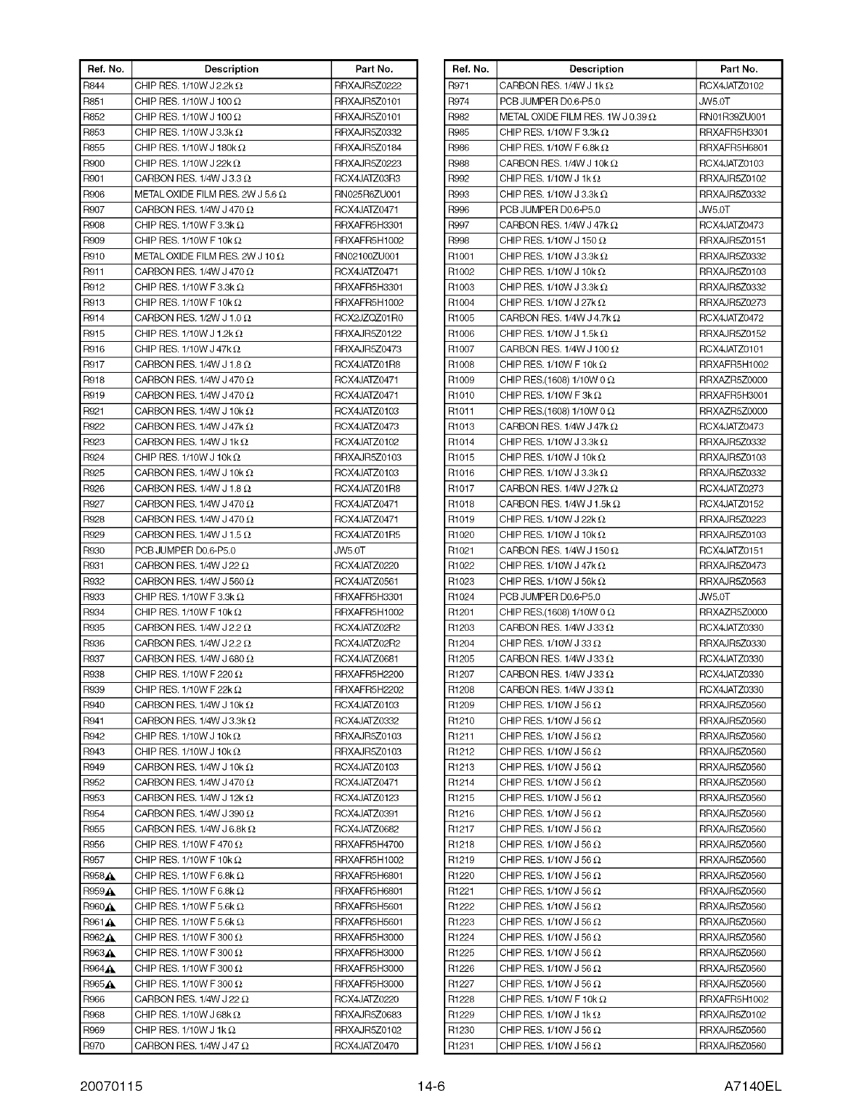
Ref, No. Description Part No.
R844 CHIP RES. 1/10W J 2.2k _ RRXAJR5Z0222
R851 CHIP RES. 1/10W J 100 _ RRXAJR5Z0101
R852 CHIP RES. 1/10W J 100 _ RRXAJR5Z0101
R853 CHIP RES. 1/10W J 3.3k _ RRXAJR5Z0332
R855 CHIP RES, 1/10W J 180k_ RRXAJR5Z0184
R900 CHIP RES. 1/10W J 22k_Z RRXAJRSZ0223
R901 CARBON RES. 1/4W J 3.3 _Z RCX4JATZ03R3
R906 METAL OXIDE FILM RES. 2W J 5.6 _Z RN025R6ZU001
R907 CARBON RES. 1/4W J 470 _ RCX4JATZ0471
R908 CHIP RES. 1/10W F 3.3k _ RRXAFRSH3301
R909 CHIP RES. 1/10W F 10k _Z RRXAFRSH1002
R910 METAL OXIDE FILM RES. 2W J 10 _ RN02100ZU001
R911 CARBON RES. 1/4W J 470 _ RCX4JATZ0471
R912 CHIP RES. 1/10W F 3.3k _ RRXAFRSH3301
R913 CHIP RES. 1/10W F 10k _Z RRXAFRSH1002
R914 CARBON RES. 1/2W J 1.0 _Z RCX2JZQZ01 R0
R915 CHIP RES. 1/10W J 1.2k_ RRXAJRSZ0122
R916 CHIP RES. 1/10W J 47k_Z RRXAJRSZ0473
R917 CARBON RES. 1/4W J 1.8 _Z RCX4JATZ01R8
R918 CARBON RES. 1/4W J 470 _ RCX4JATZ0471
R919 CARBON RES. 1/4W J 470 _ RCX4JATZ0471
R921 CARBON RES. 1/4W J 10k _ RCX4JATZ0103
R922 CARBON RES. 1/4W J 47k _ RCX4JATZ0473
R923 CARBON RES. 1/4W J lk _Z RCX4JATZ0102
R924 CHIP RES. 1/10W J 10k_Z RRXAJR5Z0103
R925 CARBON RES. 1/4W J 10k _ RCX4JATZ0103
R926 CARBON RES. 1/4W J 1.8 _Z RCX4JATZ01R8
R927 CARBON RES, 1/4W J 470 _ RCX4JATZ0471
R928 CARBON RES. 1/4W J 470 _ RCX4JATZ0471
R929 CARBON RES. 1/4W J 1.5 _Z RCX4JATZ01R5
R930 PCB JUMPER D0.6-PS.0 JWS.0T
R931 CARBON RES. 1/4W J 22 _ RCX4JATZ0220
R932 CARBON RES. 1/4W J 560 _ RCX4JATZ0561
R933 CHIP RES. 1/10W F 3.3k _ RRXAFRSH3301
R934 CHIP RES. 1/10W F 10k _Z RRXAFRSH1002
R935 CARBON RES. 1/4W J 2.2 _Z RCX4JATZ02R2
R936 CARBON RES. 1/4W J 2.2 _Z RCX4JATZ02R2
R937 CARBON RES. 1/4W J 680 _ RCX4JATZ0681
R938 CHIP RES. 1/10W F 220 _ RRXAFRSH2200
R939 CHIP RES. 1/10W F 22k _Z RRXAFRSH2202
R940 CARBON RES. 1/4W J 10k _ RCX4JATZ0103
R941 CARBON RES. 1/4W J 3.3k _Z RCX4JATZ0332
R942 CHIP RES. 1/10W J 10k_Z RRXAJRSZ0103
R943 CHIP RES. 1/10W J 10k_Z RRXAJR5Z0103
R949 CARBON RES. 1/4W J 10k _ RCX4JATZ0103
R952 CARBON RES. 1/4W J 470 _ RCX4JATZ0471
R953 CARBON RES. 1/4W J 12k _ RCX4JATZ0123
R954 CARBON RES, 1/4W J 390 _ RCX4JATZ0391
R955 CARBON RES. 1/4W J 6.8k _Z RCX4JATZ0682
R956 CHIP RES. 1/10W F 470 _ RRXAFRSH4700
R957 CHIP RES. 1/10W F 10k _Z RRXAFRSH1002
R958_i& CHIP RES. 1/10W F 6.8k _ RRXAFR5H6801
R959_ CHIP RES. 1/10W F 6.8k _ RRXAFR5H6801
R960_i& CHIP RES. 1/10W F 5.6k _ RRXAFRSH5601
R961_ CHIP RES. 1/10W F 5.6k _ RRXAFR5H5601
R962_i& CHIP RES. 1/10W F300 _ RRXAFRSH3000
R963_i& CHIP RES. 1/10W F300 _ RRXAFR5H3000
R964_, CHIP RES. 1/10W F300 _ RRXAFRSH3000
R965_, CHIP RES. 1/10W F300 _ RRXAFRSH3000
R966 CARBON RES. 1/4W J 22 _ RCX4JATZ0220
R968 CHIP RES. 1/10W J 68k_Z RRXAJRSZ0683
R969 CHIP RES. 1/10W J lk _Z RRXAJR5Z0102
R970 CARBON RES. 1/4W J 47 _ RCX4JATZ0470
Ref. No. Description Part No.
R971 CARBON RES. 1/4W J lk _,t RCX4JATZ0102
R974 PCB JUMPER D0.6-P5.0 JW5.0T
R982 METAL OXIDE FILM RES. 1W J 0.39 _,t RN01R39ZU001
R985 CHIP RES. 1/10W F 3.3k _,t RRXAFR5H3301
R986 CHIP RES. 1/10W F 6.8k _,t RRXAFR5H6801
R988 CARBON RES. 1/4W J 10k _,t RCX4JATZ0103
R992 CHIP RES. 1/10W J lk _ RRXAJR5Z0102
R993 CHIP RES. 1/10W J 3.3k _ RRXAJR5Z0332
R996 PCB JUMPER D0.6-P5.0 JW5.0T
R997 CARBON RES. 1/4W J 47k _,t RCX4JATZ0473
R998 CHIP RES, 1/10W J 150_ RRXAJR5Z0151
R1001 CHIP RES. 1/10W J 3.3k _ RRXAJRSZ0332
R1002 CHIP RES. 1/10W J 10k_Z RRXAJRSZ0103
R1003 CHIP RES. 1/10W J 3.3k _ RRXAJRSZ0332
R1004 CHIP RES. 1/10W J 27k _Z RRXAJRSZ0273
R1005 CARBON RES. 1/4W J 4.7k_ RCX4JATZ0472
R1006 CHIP RES. 1/10W J 1.5k_ RRXAJRSZ0152
R1007 CARBON RES. 1/4WJ 100_ RCX4JATZ0101
R1008 CHIP RES. 1/10W F 10k_ RRXAFR5H1002
R1009 CHIP RES.(1608) 1/10W 0 _Z RRXAZR5Z0000
R1010 CHIP RES. 1/10W F 3k_Z RRXAFR5H3001
R1011 CHIP RES.(1608) 1/10W 0 _Z RRXAZRSZ0000
R1013 CARBON RES. 1/4W J 47k _Z RCX4JATZ0473
R1014 CHIP RES. 1/10W J 3.3k_ RRXAJRSZ0332
R1015 CHIP RES. 1/10W J 10k_Z RRXAJRSZ0103
R1016 CHIP RES. 1/10W J 3.3k_ RRXAJRSZ0332
R1017 CARBON RES. 1/4W J 27k _Z RCX4JATZ0273
R1018 CARBON RES. 1/4WJ 1.5k_ RCX4JATZ0152
R1019 CHIP RES. 1/10W J 22k _Z RRXAJRSZ0223
R1020 CHIP RES. 1/10W J 10k_Z RRXAJRSZ0103
R1021 CARBON RES. 1/4WJ 150_Z RCX4JATZ0151
R1022 CHIP RES. 1/10W J 47k _Z RRXAJRSZ0473
R1023 CHIP RES. 1/10W J 56k _Z RRXAJRSZ0563
R1024 PCB JUMPER D0.6-P5.0 JWS.0T
R1201 CHIP RES.(1608) 1/10W 0 _Z RRXAZR5Z0000
R1203 CARBON RES. 1/4W J 33 _Z RCX4JATZ0330
R1204 CHIP RES. 1/10W J 33 _Z RRXAJRSZ0330
R1205 CARBON RES. 1/4W J 33 _Z RCX4JATZ0330
R1207 CARBON RES. 1/4W J 33 _Z RCX4JATZ0330
R1208 CARBON RES. 1/4W J 33 _Z RCX4JATZ0330
R1209 CHIP RES. 1/10W J 56 _Z RRXAJRSZ0560
R1210 CHIP RES. 1/10W J 56 _Z RRXAJRSZ0560
R1211 CHIP RES. 1/10W J 56 _Z RRXAJRSZ0560
R1212 CHIP RES. 1/10W J 56 _Z RRXAJRSZ0560
R1213 CHIP RES. 1/10W J 56 _Z RRXAJRSZ0560
R1214 CHIP RES. 1/10W J 56 _Z RRXAJRSZ0560
R1215 CHIP RES. 1/10W J 56 _Z RRXAJRSZ0560
R1216 CHIP RES. 1/10W J 56 _Z RRXAJRSZ0560
R1217 CHIP RES. 1/10W J 56 _Z RRXAJRSZ0560
R1218 CHIP RES. 1/10W J 56 _Z RRXAJRSZ0560
R1219 CHIP RES. 1/10W J 56 _Z RRXAJRSZ0560
R1220 CHIP RES. 1/10W J 56 _Z RRXAJRSZ0560
R1221 CHIP RES. 1/10W J 56 _Z RRXAJRSZ0560
R1222 CHIP RES. 1/10W J 56 _Z RRXAJRSZ0560
R1223 CHIP RES. 1/10W J 56 _Z RRXAJRSZ0560
R1224 CHIP RES. 1/10W J 56 _Z RRXAJRSZ0560
R1225 CHIP RES. 1/10W J 56 _Z RRXAJRSZ0560
R1226 CHIP RES. 1/10W J 56 _Z RRXAJRSZ0560
R1227 CHIP RES. 1/10W J 56 _Z RRXAJRSZ0560
R1228 CHIP RES. 1/10W F 10k_ RRXAFRSH1002
R1229 CHIP RES. 1/10W J lk_ RRXAJRSZ0102
R1230 CHIP RES. 1/10W J 56 _Z RRXAJRSZ0560
R1231 CHIP RES. 1/10W J 56 _Z RRXAJRSZ0560
20070115 14-6 A7140EL
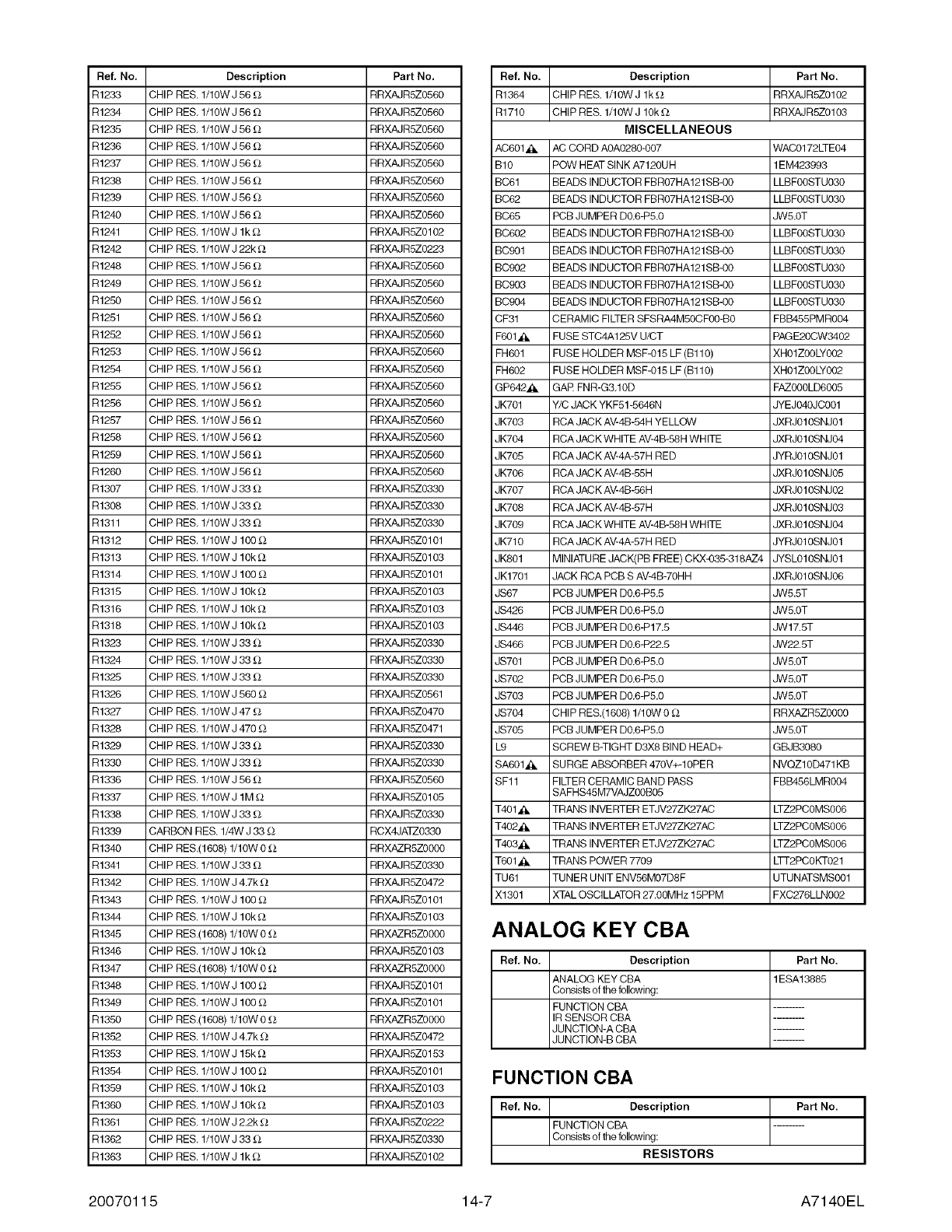
Ref, No, Description Part No,
R1233 CHIP RES. 1/10W J 56 _ RRXAJR5Z0560
R1234 CHIP RES. l/lOW J 56 _ RRXAJR5ZO560
R1235 CHIP RES. l/lOW J 56 _ RRXAJR5ZO560
R1236 CHIP RES. l/lOW J 56 _ RRXAJR5ZO560
R1237 CHIP RES. l/lOW J 56 _ RRXAJR5ZO560
R1238 CHIP RES. l/lOW J 56 _ RRXAJR5ZO560
R1239 CHIP RES. l/lOW J 56 _ RRXAJR5ZO560
R1240 CHIP RES. l/lOW J 56 _ RRXAJR5ZO560
R1241 CHIP RES. 1/IOWJ lk_,t RRXAJR5ZOlO2
R1242 CHIP RES. l/lOW J 22k _,t RRXAJR5ZO223
R1248 CHIP RES. l/lOW J 56 _ RRXAJR5ZO560
R1249 CHIP RES. l/lOW J 56 _ RRXAJR5ZO560
R1250 CHIP RES. l/lOW J 56 _ RRXAJR5ZO560
R1251 CHIP RES. l/lOW J 56 _ RRXAJR5ZO560
R1252 CHIP RES. l/lOW J 56 _ RRXAJR5ZO560
R1253 CHIP RES. l/lOW J 56 _ RRXAJR5ZO560
R1254 CHIP RES. l/lOW J 56 _ RRXAJR5ZO560
R1255 CHIP RES. l/lOW J 56 _ RRXAJR5ZO560
R1256 CHIP RES. l/lOW J 56 _ RRXAJR5ZO560
R1257 CHIP RES. l/lOW J 56 _ RRXAJR5ZO560
R1258 CHIP RES. l/lOW J 56 _ RRXAJR5ZO560
R1259 CHIP RES. l/lOW J 56 _ RRXAJR5ZO560
R1260 CHIP RES. l/lOW J 56 _ RRXAJR5ZO560
R1307 CHIP RES. l/lOW J 33 _ RRXAJR5ZO330
R1308 CHIP RES. l/lOW J 33 _ RRXAJR5ZO330
R1311 CHIP RES. l/lOW J 33 _ RRXAJR5ZO330
R1312 CHIP RES. 1/IOWJ lOO_ RRXAJR5ZOlOl
R1313 CHIP RES. l/lOW J 1Ok_,t RRXAJR5ZOlO3
R1314 CHIP RES. 1/IOWJ lOO_ RRXAJR5ZOlOl
R1315 CHIP RES. l/lOW J 1Ok_,t RRXAJR5ZOlO3
R1316 CHIP RES. l/lOW J 1Ok_,t RRXAJR5ZOlO3
R1318 CHIP RES. l/lOW J 1Ok_,t RRXAJR5ZOlO3
R1323 CHIP RES. l/lOW J 33 _ RRXAJR5ZO330
R1324 CHIP RES. l/lOW J 33 _ RRXAJR5ZO330
R1325 CHIP RES. l/lOW J 33 _ RRXAJR5ZO330
R1326 CHIP RES. l/lOW J 560 _ RRXAJR5ZO561
R1327 CHIP RES. l/lOW J 47 _ RRXAJR5ZO470
R1328 CHIP RES. l/lOW J 470 _ RRXAJR5ZO471
R1329 CHIP RES. l/lOW J 33 _ RRXAJR5ZO330
R1330 CHIP RES. l/lOW J 33 _ RRXAJR5ZO330
R1336 CHIP RES. l/lOW J 56 _ RRXAJR5ZO560
R1337 CHIP RES. l/lOW J 1M _,t RRXAJR5ZOlO5
R1338 CHIP RES. l/lOW J 33 _ RRXAJR5ZO330
R1339 CARSON RES. 1/4W J 33 _ RCX4JATZO330
R1340 CHIP RES.(1608) l/lOW O_ RRXAZR5ZOOOO
R1341 CHIP RES. l/lOW J 33 _ RRXAJR5ZO330
R1342 CHIP RES. l/lOW J 4.7k_ RRXAJR5ZO472
R1343 CHIP RES. l/lOW J lOO_ RRXAJR5ZOlOl
R1344 CHIP RES. l/lOW J 1Ok_,t RRXAJR5ZOlO3
R1345 CHIP RES.(1608) l/lOW O_ RRXAZRSZOOOO
R1346 CHIP RES. l/lOW J 1Ok_,t RRXAJR5ZOlO3
R1347 CHIP RES.(1608) l/lOW O_ RRXAZR5ZOOOO
R1348 CHIP RES. l/lOW J lOO_ RRXAJR5ZOlOl
R1349 CHIP RES. 1/IOWJ lOO_ RRXAJR5ZOlOl
R1350 CHIP RES.(1608) l/lOW O_ RRXAZR5ZOOOO
R1352 CHIP RES. l/lOW J 4.7k_ RRXAJR5ZO472
R1353 CHIP RES. l/lOW J 15k _,t RRXAJR5ZO153
R1384 CHIP RES. l/lOW J lOO_ RRXAJR5ZOlOl
R1359 CHIP RES. l/lOW J 1Ok_,t RRXAJR5ZOlO3
R1360 CHIP RES. l/lOW J 1Ok_,t RRXAJR5ZOlO3
R1361 CHIP RES. l/lOW J 2.2k _ RRXAJR5ZO222
R1362 CHIP RES. l/lOW J 33 _ RRXAJR5ZO330
R1363 CHIP RES. 1/IOWJ lk_,t RRXAJR5ZOlO2
Ref, No. Description Part No.
R1364 CHIP RES. 1/10W J lk_ RRXAJR5Z0102
R1710 CHIP RES. l/lOW J 1Ok_,t RRXAJRSZOlO3
MISCELLANEOUS
AC6Ol_. AC CORD AOAO280-OO7 WACO172LTEO4
BlO POW HEAT SINK A712OUH 1EM423993
BC61 BEADS INDUCTOR FBRO7HA121SB-OO LLBFOOSTUO3O
BC62 BEADS INDUCTOR FBRO7HA121SB-OO LLBFOOSTUO3O
BC65 PCB JUMPER DO.6-P5.O JW5.OT
BC6O2 BEADS INDUCTOR FBRO7HA121SB-OO LLBFOOSTUO3O
BCgOl BEADS INDUCTOR FBRO7HA121SB-OO LLBFOOSTUO3O
Bcgo2 BEADS INDUCTOR FBRO7HA121SB-OO LLBFOOSTUO3O
Bcgo3 BEADS INDUCTOR FBRO7HA121SB-OO LLBFOOSTUO3O
Bcgo4 BEADS INDUCTOR FBRO7HA121SB-OO LLBFOOSTUO3O
CF31 CERAMIC FILTER SFSRA4MSOCFOO-BO FBB455PMROO4
F601_. FUSE STC4A125V U/CT PAGE2OCW3402
FH6Ol FUSE HOLDER MSF-015 LF (B110) XHO1ZOOLYOO2
FH6O2 FUSE HOLDER MSF-015 LF (B110) XHO1ZOOLYOO2
GP642_, GAR FNR-G3,1OD FAZOOOLD6OO5
JK701 Y/C JACK YKF51-5646N JYEJ040JC001
JK703 RCA JAC K AV-4B-54H YELLOW JXRJ010SNJ01
JK704 RCA JACK WHITE AV-4B-58H WHITE JXRJ010SNJ04
JK705 RCA JACK AV-4A-57H RED JYRJ010SNJ01
JK706 RCA JACK AV-4B-55H JXRJ010SNJ05
JK707 RCA JACK AV-4B-56H JXRJ010SNJ02
JK708 RCA JACK AV-4B-87H JXRJ010SNJ03
JK709 RCA JACK WHITE AV-4B-58H WHITE JXRJ010SNJ04
JK710 RCA JACK AV-4A-57H RED JYRJ010SNJ01
JK801 MINIATURE JACK(PB FREE) CKX-035-318AZ4 JYSL010SNJ01
JK1701 JACK RCA PCB S AV-4B-70HH JXRJ010SNJ06
JS67 PCB JUMPER D0.6-P5.5 JW5.ST
JS426 PCB JUMPER D0.6-PS.0 JW5.0T
JS446 PCB JUMPER D0.6-P17.5 JW17.5T
JS466 PCB JUMPER D0.6-P22.5 JW22.5T
JS701 PCB JUMPER D0.6-P5.0 JW5.0T
JS702 PCB JUMPER D0.6-P5.0 JW5.0T
JS703 PCB JUMPER D0.6-PS.0 JW5.0T
JS704 CHIP RES.(1608) 1/10W 0 _Z RRXAZRSZ0000
JS708 PCB JUMPER D0.6-PS.0 JW5.0T
L9 SCREW B-TIGHT D3X8 BIND HEAD+ GBJB3080
SA601_, SURGE ABSORBER 470V+-10PER NVQZ10D471KB
SF11 FILTER CERAMIC BAND PASS FBB456LMR004
SAFHS45M7VAJZ00B05
T401_, TRANS INVERTER ETJV27ZK27AC LTZ2PC0MS006
T402_, TRANS INVERTER ETJV27ZK27AC LTZ2PC0MS006
T403_i_ TRANS INVERTER ETJV27ZK27AC LTZ2PC0MS006
T601_i_ TRANS POWER 7709 L]q-2PC0KT021
TU61 TUNER UNIT ENV56M07D8F UTUNATSMS001
X1301 XTAL OSCILLATOR 27.00MHz 15PPM FXC276LLN002
ANALOG KEY CBA
Ref, No. Part No.
1ESA13885
Description
ANALOG KEY CBA
Consists of the following:
FUNCTION CSA
IR SENSOR CBA
JUNCTION-A CBA
JUNCTION-B CSA
FUNCTION CBA
Part No.
Description
FUNCTION CBA
Consists of the following:
RESISTORS 1
20070115 14-7 A7140EL
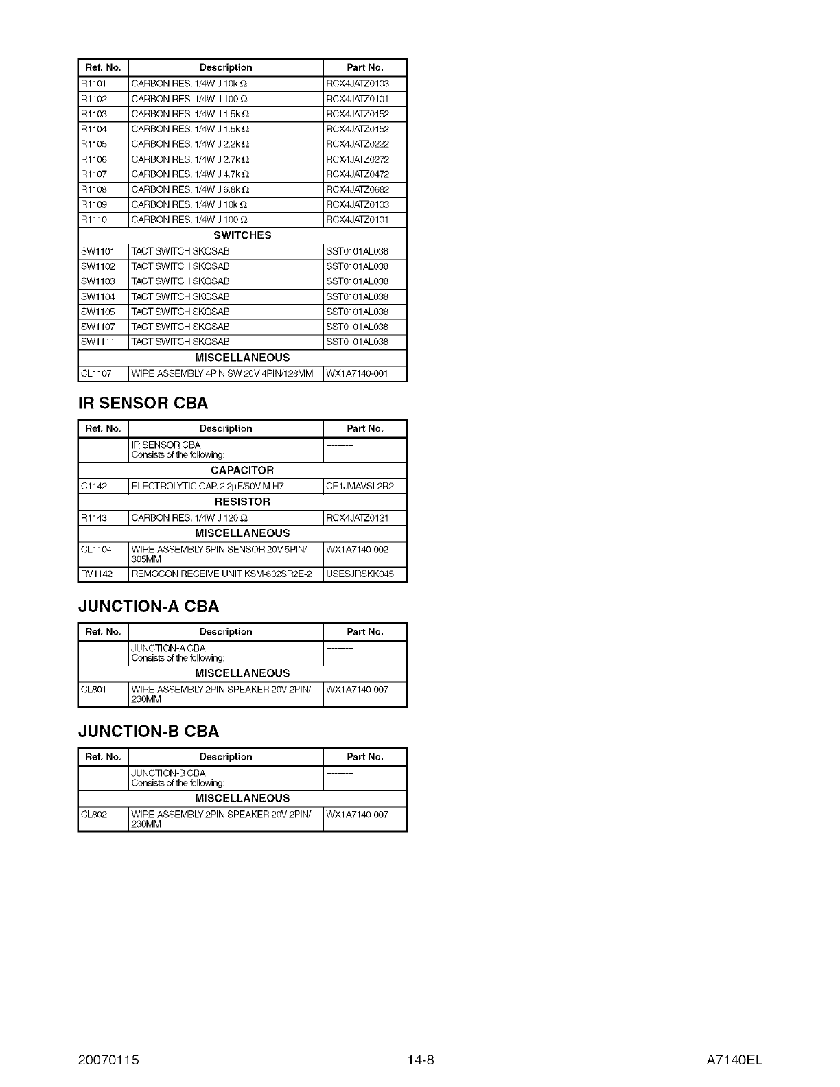
Ref, No. Description Part No.
Rl101 CARBON RES. 1/4WJ 10k_ RCX4JATZ0103
Rl102 CARBON RES. 1/4WJ 100_ RCX4JATZ0101
Rl103 CARBON RES. 1/4WJ 1.5k _,t RCX4JATZ0152
Rl104 CARBON RES. 1/4WJ 1.5k _,t RCX4JATZ0152
Rl105 CARBON RES. 1/4W J 2.2k _,t RCX4JATZ0222
Rl106 CARBON RES. 1/4W J 2.7k _,t RCX4JATZ0272
Rl107 CARBON RES. 1/4W J 4.7k _,t RCX4JATZ0472
Rl108 CARBON RES. 1/4W J 6.8k _,t RCX4JATZ0682
Rl109 CARBON RES. 1/4WJ 10k_ RCX4JATZ0103
Rl110 CARBON RES. 1/4WJ 100_ RCX4JATZ0101
SWITCHES
SWl101 TACT SWITCH SKQSAB SST0101AL038
SW1102 TACT SWITCH SKQSAB SST0101AL038
SW1103 TACT SWITCH SKQSAB SST0101AL038
SW1104 TACT SWITCH SKQSAB SST0101AL038
SW1105 TACT SWITCH SKQSAB SST0101AL038
SW1107 TACT SWITCH SKQSAB SST0101AL038
SW1111 TACT SWITCH SKQSAB SST0101AL038
MISCELLANEOUS
CLl107 IWIRE ASSEMBLY 4PIN SW 20V 4PIN/128MM IWX1A7140-001
IR SENSOR CBA
Description tPartNo,
IR SENSOR CBA .........
Consists of the following:
CAPACITOR
ELECTROLYTIC CAR 2.2pg/s0v M H7 LCE1JMAVSL2R2
RESISTOR
Rl143 ICARBON RES. 1/4W J 120 _ /RCX4JATZ0121
MISCELLANEOUS
CLl104 IWIRE ASSEMBLY 5PIN SENSOR 20V 5PIN/ WX1A7140-002
305MM
RV_CON RECEIVE UNIT KSM-602SR2E-2 USESJRSKK045
JUNCTION-A CBA
Description t_..PartNo.
JUNCTION-A CBA .........
Consists of the following:
MISCELLANEOUS
CL801 IWIRE ASSEMBLY 2PIN SPEAKER 20V 2PIN/ |WX1A7140-007
_____230MM [
JUNCTION-B CBA
Description t_..PartNo.
JUNCTION-B CBA .........
Consists of the following:
MISCELLANEOUS
CL802 IWIRE ASSEMBLY 2PIN SPEAKER 20V 2PIN/ |WX1A7140-007
......._ 230MM [
20070115 14-8 A7140EL
© 2007FunaiElectricCo.,Ltd.
Allrightsreserved.Nopartofthismanualmaybereproduced,copied,transmitted,disseminated,transcribed,
downloadedorstoredinanystoragemedium,inanyformorforanypurposewithouttheexpresspriorwritten
consentof Funai.Furthermore,anyunauthorizedcommercialdistributionofthismanualoranyrevisionhereto
isstrictlyprohibited.
Informationinthisdocumentissubjecttochangewithoutnotice.Funaireservestherighttochangethecontent
hereinwithouttheobligationto notifyanypersonororganizationofsuchchanges.
F_UNA!withthe(j designisa registeredtrademarkof FunaiElectricCo.,Ltdandmaynotbeusedinanyway
withouttheexpresswrittenconsentofFunai.Allothertrademarksusedhereinremaintheexclusivepropertyof
theirrespectiveowners.Nothingcontainedinthismanualshouldbeconstruedasgranting,byimplicationor
otherwise,anylicenseorrightto useanyofthetrademarksdisplayedherein.Misuseofanytrademarksorany
othercontentinthismanualisstrictlyprohibited.Funaishallaggressivelyenforceitsintellectualpropertyrights
tothefullestextentofthelaw.
LC200SL8
A7140UH
2007-02-02
