Synapse Wireless RF26X RF26X Module User Manual 10 0339 Manual
Synapse Wireless Inc. RF26X Module 10 0339 Manual
Manual

5015 B.U. Bowman Drive Buford, GA 30518 USA Voice: 770-831-8048 Fax: 770-831-8598
Certification Exhibit
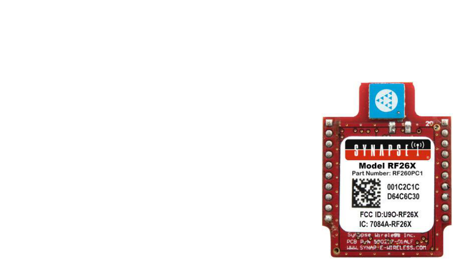
FCC ID: U9O-RF26X
FCC Rule Part: 15.247
IC Radio Standards Specification: RSS-210
ACS Report Number: 10-0339.W06.11.A
Manufacturer: Synapse Wireless Inc.
Model: RF26X
Manual

DATA SHEET
RF Engine® 26X Series
Model Number: RF26X
Part Numbers: RF260PC1
RF261PC1
RF266PC1
Document Revision v1.0
© 2011 Synapse, All Rights Reserved
All Synapse products are patented or patent pending
Specifications are subject to change without notice – confirm that data is current
Synapse, the Synapse logo, SNAP, and Portal are all registered trademarks of
Synapse Wireless, Inc.
500 Discovery Drive
Huntsville, Alabama 35806
877-982-7888
Doc # 430141-01A

RF26X Data Sheet Document Number 430141-01A Page 2 of 14

RF26X Data Sheet Document Number 430141-01A Page 3 of 14
Table of Contents
1.0 RF26X OEM Module Overview 4
1.1 Specifications 5
1.2 Module Pin Definitions 6
1.3 Electrical Characteristics 6
1.4 Mechanical Drawings 8
1.5 Board Mounting Configurations 8
2.0 Agency Certifications 9
2.1 United States (FCC) 9
2.1.1 OEM Labeling Requirements 9
2.1.2 FCC Notices 10
2.1.3 FCC Approved Antennas 11
2.2 Canada (IC) 13
2.2.1 OEM Labeling Requirements 13
RF26X Data Sheet Document Number 430141-01A Page 4 of 14
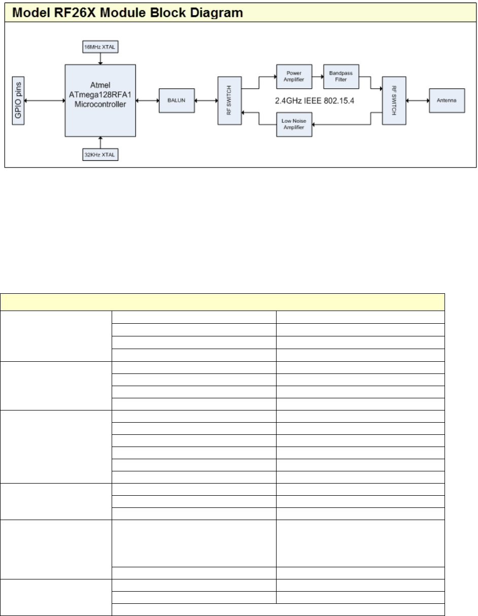
1.0 RF Engine 26X Series OEM Modules Overview
The RF Engine 26X Series (Model Number RF26X) is an IEEE 802.15.4, low power,
highly-reliable solution to embedded wireless control and monitoring network needs that
require high data rates. The Model RF26X is pin-compatible with Digi International’s
XBee and XBee-PRO RF modules.
The RF26X embeds Synapse’s SNAP OS, the industry’s first Internet-enabled, wireless
mesh network operating system into the Atmel ATmega128RFA1 single-chip AVR®
microcontroller with an integrated transceiver that delivers up to 2Mbits/sec. These low-
cost modules can have a range of up to 4,000 feet and power consumption as low as
0.37 μA to enable a new generation of battery-driven systems.
SNAP’s on-board Python interpreter provides for rapid application development and
over-the-air programming, while Atmel’s low-power RF single-chip design saves board
space and lowers the overall Bill of Materials and power consumption. The RF26X is
approved as an FCC Part 15 unlicensed modular transmitter. The modules provide up
to 16 channels of operation in the ISM 2.4GHz frequency band. The RF26X contains
both a power amplifier for transmission and a low noise amplifier in the receive path for
extended range.
This Data Sheet details Part Numbers RF260PC1, RF261PC1 and RF266PC1
• 15 GPIO, 4 with 10-bit ADC
• 128k flash, 56k free for over-the-air uploaded user apps
• One UART port –
260PC1: up to 115.2kbps
261PC1: up to 1Mbps
266PC1: up to 1Mbps
• Low power modes: 0.37 μA w/ internal timer running
• Spread spectrum (DSSS) technology
• Socket-able or solder-able
• Up to 2 Mbps Data Rate
• 2.4 GHz RF Frequency
• Receive Amplifier (10 dBm) standard
• Transmit amplifier (20 dBm) for best-in-class range
• Chip antenna (up to 4000 feet, LoS at 250kbps)
RF26X Data Sheet Document Number 430141-01A Page 5 of 14
Figure 1.0 Block diagram showing the major subsystems comprising the RF26X
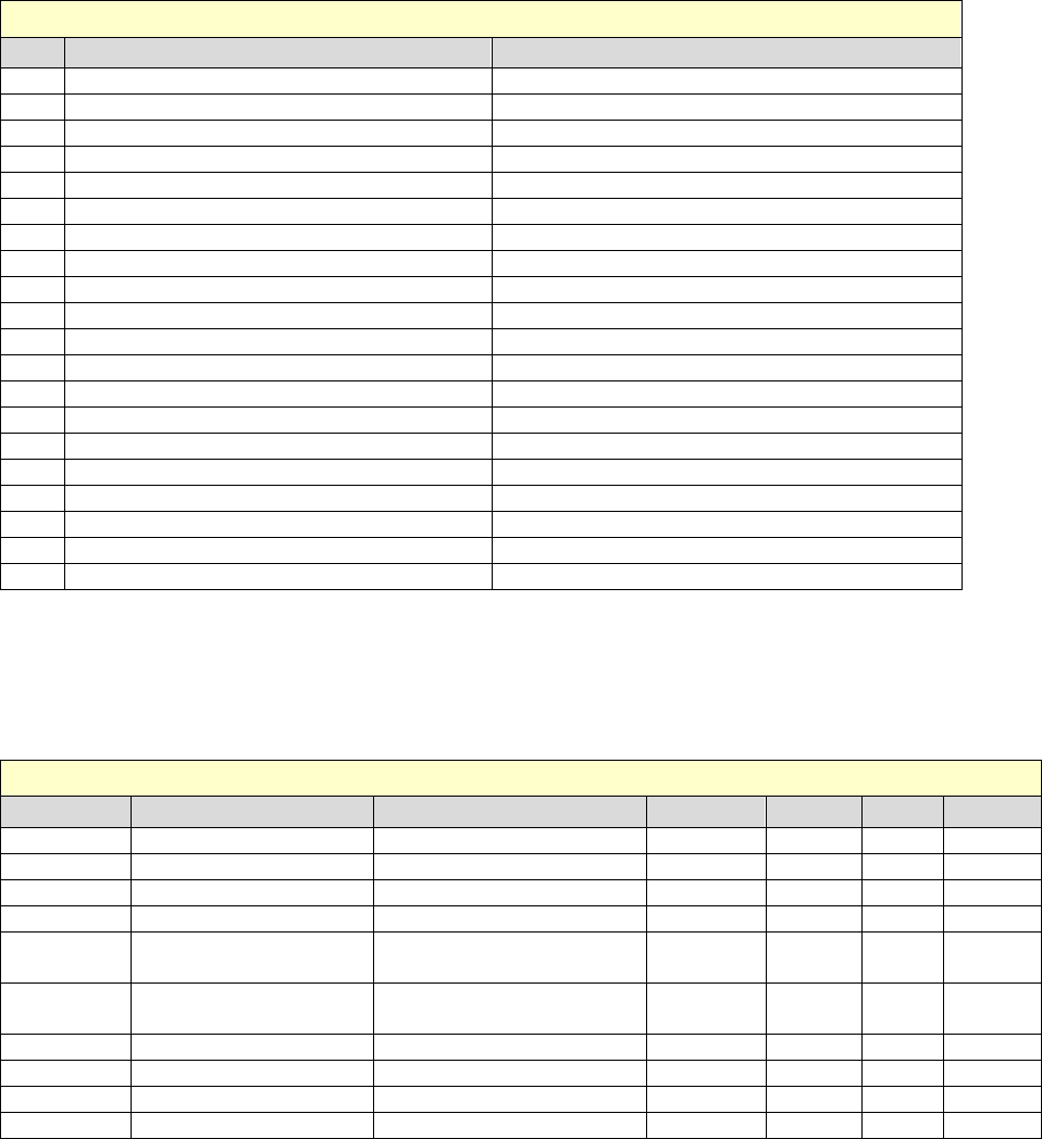
1.1 Specifications
Table 1.0. RF26X Specifications
Performance
Outdoor LOS Range
Up to 4,000 feet at 250Kbps
Transmit Power Output
20 dBm
RF Data Rate
250Kbps, 500Kbps, 1Mbps, 2Mbps
Receiver Sensitivity -107 dBm (1% PER)
Power Requirements
Supply Voltage
2.7 - 3.6 V
Transmit Current (Typ@3.3V)
130mA
Idle/Receive Current (Typ@3.3V)
25mA
Power-down Current (Typ@3.3V)
0.37uA
General
Frequency
ISM 2.4 GHz
Spreading Method
Direct Sequence (DSSS)
Modulation
O-QPSK
Dimensions
1.3" (H) x 1.0" (W)
Operating Temperature
- 40 to 85 deg C.
Antenna Options
Chip
Networking
Topology
SNAP
Error Handling
Retries and acknowledgement
Number of Channels
16
Available I/O UARTS with HW Flow Control
One UART port:
260PC1 – up to 115.2kbps
261PC1 – up to 1Mbps
266PC1 – up to 1Mbps
GPIO
15 total; 4 with 10bit ADC
Agency Approvals
FCC Part 15.247
FCC ID: U9O-RF26X
Industry Canada (IC)
IC: 7084A-RF26X
CE available as a custom part. Call 1-877-982-7888
RF26X Data Sheet Document Number 430141-01A Page 6 of 14
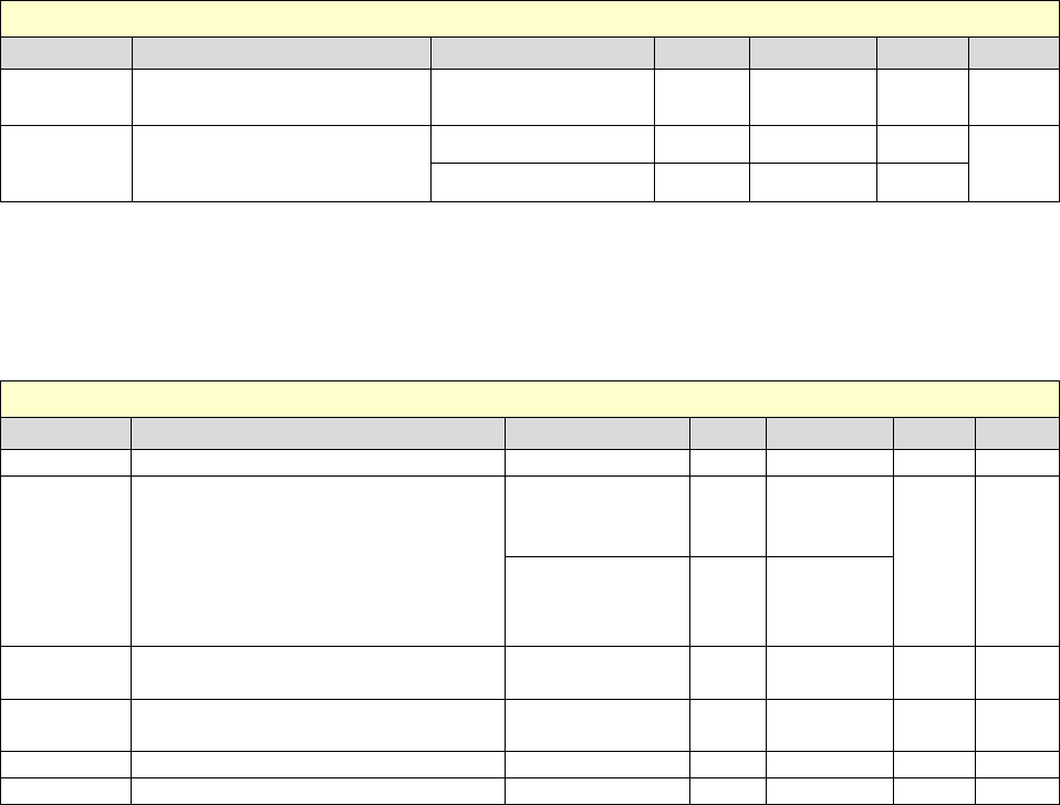
1.2 Module Pin Definitions
Table 1.1. RF26X Module Pin Assignments
Pin
Name
Description
1
3.3V
Power Supply
2
IO_11 PD3 INT3 TXD1
IO_11, UART Data Out, Interrupt
3
IO_10 PD2 INT2 RXD1
IO_10, UART Data In, Interrupt
4
IO_21 PE5 INT5 OC3C
IO_21, PWM, Interrupt
5
RESET
Module Reset, Active Low
6
IO_20 PE4 INT4 OC3B
IO_20, PWM, Interrupt
7
IO_19 PE3 RTS0 OC3A AIN0
IO_19, PWM
8
-
No Connect
9
IO_9 PD1 INT1
IO_9, Interrupt
10
GND
11
IO_15 PD7
IO_15
12
IO_12 PD4 CTS1 ICP1
IO_12, CTS Output
13
IO_8 PD0 INT0
IO_8, Interrupt
14
-
No Connect
15
IO_37 PG5 OC0B
IO_37, PWM
16
IO_23 PE7 INT7 ICP3
IO_23, RTS Input, Interrupt
17
IO_31 PF7 ADC7
IO_31, ADC7 Input
18
IO_30 PF6 ADC6
IO_30, ADC6 Input, SPI MOSI
19
IO_29 PF5 ADC5
IO_29,ADC5 Input, SPI SCLK
20
IO_28 PF4 ADC4
IO_28,ADC4 Input, SPI MISO
1.3 Electrical Characteristics
Table 1.2. RF26X DC Characteristics
Symbol
Parameter
Condition
Min
Typ 1
Max
Units
VCC 2
Supply Voltage
2.7
3.3
3.6
V
TOP
Operating Temp
-40
85
°C
VIH
Input Hi Voltage
All Digital Inputs
VCC - 0.4
V
VIL
Input Low Voltage
All Digital Inputs
0.4
V
VOL Output Low Voltage All drive strengths
(2,4,6,8 mA)
0.4 V
VOH Output High Voltage
All drive strengths
(2,4,6,8 mA)
VCC - 0.4 V
ILIN
In Leakage Current
VIN=VCC or VSS, all Pins
TBD
uA
TX-ICC
Transmit Current
VCC = 3.3V
80
mA
RX-ICC
Receive Current
20
mA
SHDN-ICC
Sleep Current
VCC = 3.3V
1.6
uA
1 All typical specifications are measured at 25°C.
2 Absolute maximum stress rated voltage for VCC is -0.3 to 3.6. It is recommended that a bulk decoupling capacitor (47 uF
tantalum rated at 6.3volts) be located close to the VCC pin 21 of the RF26X connector on host board.
RF26X Data Sheet Document Number 430141-01A Page 7 of 14
Table 1.3. ADC Electrical Characteristics (Operating)
Symbol
Parameter
Condition
Min
Typical
Max
Unit
VREFH3 Voltage Reference, High Programmable 1.5 1.6 1.8 V
VINDC Analog input voltage Single Ended 0 1.8 V
Differential4 0 3.3
3 VREFH is programmable to three fixed values; 1.5V, 1.6V, and 1.8V. The default is 1.6V.
4 Each differential analog input may be as high as 3.3V but the differential voltage is still limited.
Table 1.4. ADC Timing/Performance Characteristics
Symbol
Parameter
Condition
Min
Typical
Max
Unit
RAS
Source impedance at input5
3k
kΩ
RES Conversion Resolution
Single Ended
CLKADC <=
4MHz 10
Bits
Single Ended
CLKADC >
8MHz 8
DNL Differential non-linearity
V
REFH = 1.6V
CLKADC=4MHz
-0.5 LSB
INL Integral non-linearity
V
REFH = 1.6V
CLKADC=4MHz
0.8 LSB
EZS
Zero-scale error
1.5
LSB
EG
Gain error
1
LSB
5 Any analog source with a source impedance greater the 3kΩ will increase the sampling time.
RF26X Data Sheet Document Number 430141-01A Page 8 of 14
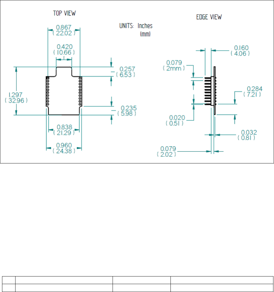
1.4 Mechanical Drawings
These drawings in Figure 1.1 show the RF26X module mechanical specifications.
Figure 1.1 Mechanical drawings of the RF26X Module
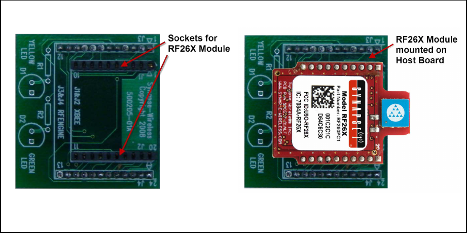
1.5 Board Mounting Considerations
The RF26X module is designed to mount into a receptacle (socket) on the host board.
Picture 1.1 shows an RF26X module plugged in to an example host board. The
receptacle sockets are on standard 2mm centers. Suggested receptacles to be used on
the host are:
1)
Thru-hole receptacle
Samtec
MMS-110-01-L-SV
2)
Surface mount receptacle
Samtec
MMS-110-02-L-SV
RF26X Data Sheet Document Number 430141-01A Page 9 of 14
Host Board Example RF26X Mounted
Picture 1.1 RF26X Mounted To Host Board
2.0 Agency Certifications
2.1 United States (FCC)
The Model RF26X modules comply with Part 15 of the FCC rules and regulations.
Compliance with the labeling requirements, FCC notices and antenna usage guidelines
is required. In order to comply with FCC Certification requirements, the Original
Equipment Manufacturer (OEM) must fulfill the following requirements.
1. The system integrator must place an exterior label on the outside of the final
product housing the RF26X Modules. Figure 2.1 below shows the contents that
must be included in this label.
2. RF26X Modules may only be used with the antenna that has been tested and
approved for use with the module. Please refer to the antenna table provided in
this section.
2.1.1 OEM Labeling Requirements
NOTICE: The OEM must make sure that FCC labeling requirements are met. This
includes a clearly visible exterior label on the outside of the final product housing that
displays the contents shown in Figure 2.1 below.

RF26X Data Sheet Document Number 430141-01A Page 10 of 14
2.1.2 FCC Notices
WARNING: The RF26X modules have been tested by the FCC for use with other
products without further certification (as per FCC Section 2.1091). Changes or
modifications to this device not expressly approved by Synapse Wireless Inc. could void
the user’s authority to operate the equipment.
NOTICE: OEM’s must certify final end product to comply with unintentional radiators
(FCC Section 15.107 and 15.109) before declaring compliance of their final product to
Part 15 of the FCC Rules.
NOTICE: The RF26X modules have been certified for remote and base radio
applications. If the module will be used for portable applications, the device must
undergo SAR testing.
This equipment has been tested and found to comply with the limits for a Class B digital
device, pursuant to Part 15 of the FCC Rules. These limits are designed to provide
reasonable protection against harmful interference in a residential installation. This
equipment generates, uses, and can radiate radio frequency energy and, if not installed
and used in accordance with the instructions, may cause harmful interference to radio
communications. However, there is no guarantee that interference will not occur in a
particular installation.
If this equipment does cause harmful interference to radio or television reception, which
can be determined by turning the equipment off and on, the user is encouraged to try to
correct the interference by one or more of the following measures:
• Reorient or relocate the receiving antenna.
• Increase the separation between the equipment and receiver.
• Connect the equipment into an outlet on a circuit different from that to which the
receiver is connected.
• Consult the dealer or an experienced radio/TV technician for help.
MANUFACTURERS NAME Figure 2.1 FCC Label
BRAND NAME or TRADE NAME
Contains RF26X FCC ID: U9O-RF26X
This device complies with Part 15 of the FCC Rules. Operation is subject to the following
two conditions: (1) This device may not cause harmful interferences, and (2) this device
must accept any interference received, including interference that may cause undesired
operation.

RF26X Data Sheet Document Number 430141-01A Page 11 of 14
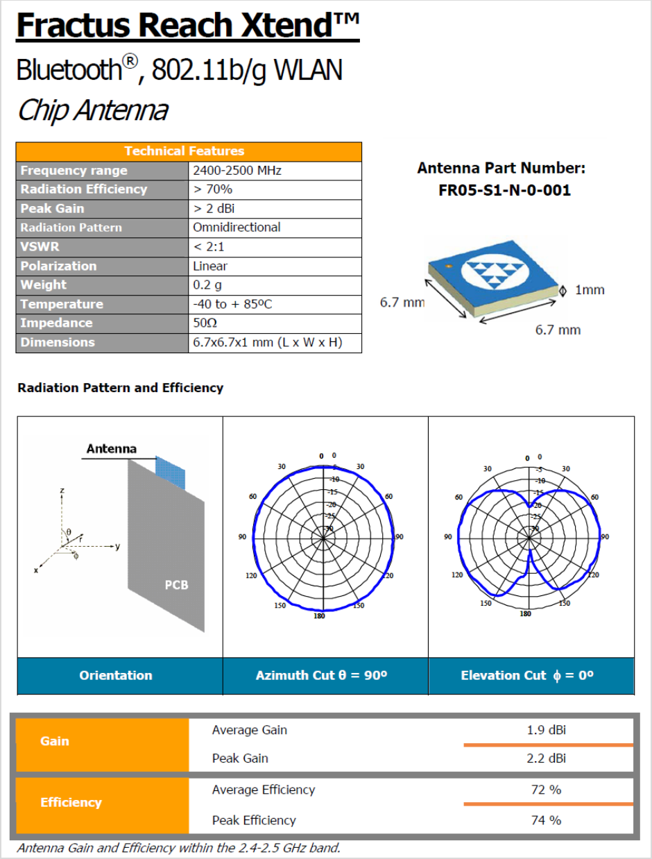
2.1.3 FCC Approved Antennas
The RF26X modules are FCC-approved for fixed base station and mobile applications.
The FCC requirement for mobile applications states that the antenna must be mounted
at least 20 cm (8 in) from nearby persons.
Notice: To reduce potential radio interference to other users, the antenna type and its
gain should be chosen so that the equivalent isotropically radiated power (e.i.r.p.) is not
more than that permitted for successful communication. This module has been
designed to operate with the antennas listed below in Table 2.1. The required antenna
impedance is 50 ohms.
Table 2.1. Approved FCC Antennas
Part Number
Type
Gain
Application
Min. Separation
Fractus: FR05-S1-N-0-001
Chip Antenna
1.9 dBi
Fixed/Mobile
20 cm.
Recommended Antenna:
(Next Page)
RF26X Data Sheet Document Number 430141-01A Page 12 of 14
RF26X Data Sheet Document Number 430141-01A Page 13 of 14
RF Exposure WARNING:
This equipment complies with FCC radiation exposure limits set forth for an uncontrolled
environment. This equipment should be installed and operated with minimum distance
20cm between the radiator and your body. This transmitter must not be co-located or
operating in conjunction with any other antenna or transmitter.
NOTICE: The preceding statement must be included as a CAUTION statement in OEM
product manuals in order to alert users of FCC RF Exposure compliance.
2.2 Canada (IC)
This device complies with Industry Canada license-exempt RSS standard(s). Operation
is subject to the following two conditions: (1) this device may not cause interference,
and (2) this device must accept any interference, including interference that may cause
undesired operation of the device.
Under Industry Canada regulations, this radio transmitter may only operate using an
antenna of a type and maximum (or lesser) gain approved for the transmitter by Industry
Canada. To reduce potential radio interference to other users, the antenna type and its
gain should be so chosen that the equivalent isotropically radiated power (e.i.r.p.) is not
more than that necessary for successful communication.
This radio transmitter Model: RF26X, IC: 7084A-RF26X has been approved by Industry
Canada to operate with the antenna types listed below with the maximum permissible
gain and required antenna impedance for each antenna type indicated. Antenna types
not included in this list, having a gain greater than the maximum gain indicated for that
type, are strictly prohibited for use with this device.
Table 2.2. Approved FCC Antennas
Part Number
Type
Gain
Application
Min. Separation
Fractus: FR05-S1-N-0-001
Chip Antenna
1.9 dBi
Fixed/Mobile
20 cm.
2.2.1 OEM Labeling Requirements
Labeling requirements for Industry Canada are similar to those of the FCC. A clearly
visible label on the outside of the final product housing must display the contents shown
in Figure 2.2 below.
MANUFACTURERS NAME Figure 2.2 IC Label
BRAND NAME or TRADE NAME
MODEL:
Contains RF Engine IC: 7084A-RF26X

RF26X Data Sheet Document Number 430141-01A Page 14 of 14
NOTE: The OEM can choose to implement a single label combined for both FCC and
IC labeling requirements. If a combined single label is chosen, there must be a clearly
visible label on the outside of the final product housing displaying the contents shown in
Figure 2.3 below.
MANUFACTURERS NAME Figure 2.3 Combined FCC and IC Label
BRAND NAME or TRADE NAME
Contains RF Engine FCC ID: U9O-RF26X
Contains RF Engine IC: 7084A-RF26X
This device complies with Part 15 of the FCC Rules. Operation is subject to the
following two conditions: (1) This device may not cause harmful interferences, and (2)
this device must accept any interference received, including interference that may cause
undesired operation.