Synapse Wireless SM200 SM200 Module User Manual 11 0216 Exhibit Cover
Synapse Wireless Inc. SM200 Module 11 0216 Exhibit Cover
UserManual.wiki
>
Synapse Wireless
>
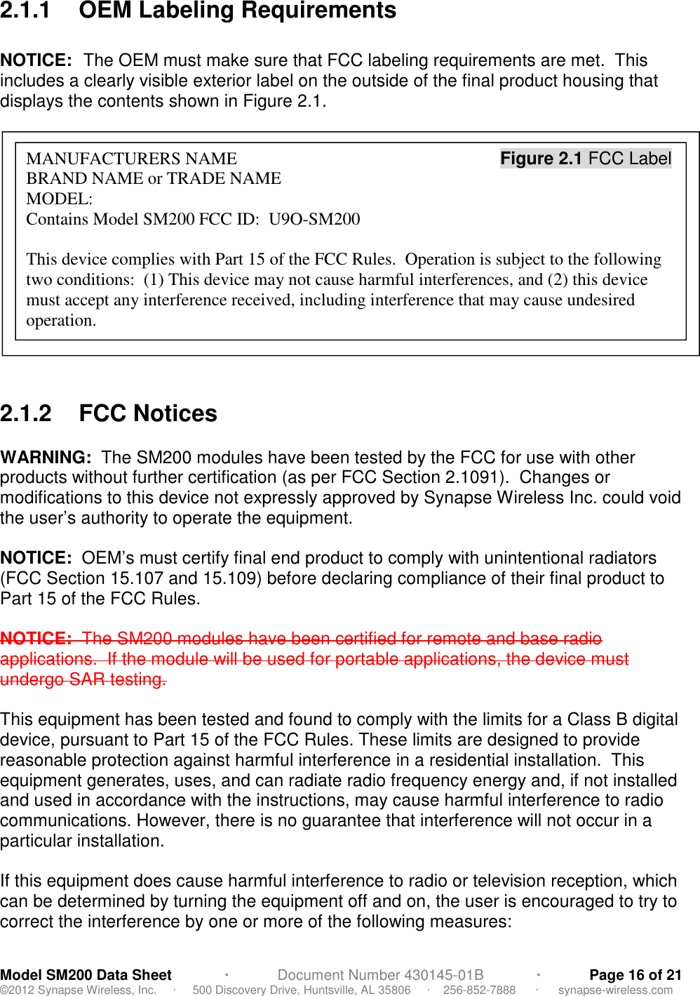
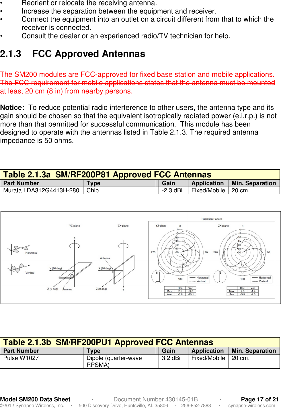
SM200 User Manual
Manual
Navigation menu
Upload a User Manual
Namespaces
Wiki Guide
HTML
PDF
Info
Views
User Manual
Discussion / Help
Navigation