TAIYO YUDEN WYSAAVKXY WIRELESS LAN MODULE User Manual
Taiyo Yuden Co., Ltd. WIRELESS LAN MODULE
User manual
26-Feb.-2014 Ver0.3
TAIYO YUDEN
TAIYO YUDEN 1/26
GT WYSAAVKXY
Wireless LAN Module
IEEE802.11b/g/n
GT WYSAAVKXY
User Manual
In case you adopt this module and design some appliance, please
ask for the latest specifications from the local sales office.
26-Feb.-2014 Ver0.3
TAIYO YUDEN
TAIYO YUDEN 2/26
GT WYSAAVKXY
Document constituent list
Control name Control No. Document Page
General Items HD-AG-A131203 1/6 - 6/6
Absolute maximum ratings HD-AM-A131203 1/1
Electrical characteristics HD-AE-A131203 1/11 – 11/11
Circuit schematic HD-MC-A131203 1/1
Outline / Appearance HD-AD-A131203 1/2 - 2/2
Pin Layout HD-BA-A131203 1/2 - 2/2
Reflow profile 1/1
Rev. record
16-Jan.-2014> Ver.0.1 Release
14-Feb-2014> Ver.0.2 General Items up date
26-Feb-2014> Ver.0.3 General Items up date
vi)-b) and vii)-c) minimum separation distance: corrected from 5.9cm to 52mm

26-Feb.-2014 Ver0.3
TAIYO YUDEN
TAIYO YUDEN 3/26
GT WYSAAVKXY
Control No.
HD-AG-A131203 (1/6)
Control name
General Items
(1)Scope
適用
This specification (“Specification”) applies to the hybrid IC “WYSAAVKXY” for use Wireless LAN
Module (“Product”) manufactured by TAIYO YUDEN CO.,LTD. (“TAIYO YUDEN”)
本仕様書は、太陽誘電株式会社(“弊社”)により製造される Wireless LAN 用ハイブリッド IC
“WYSAAVKXY” (“本製品”)に適用する。
(2)Description
内容
① Part Number : WYSAAVKXY
品 名 : WYSAAVKXY
② Function : Radio frequency transceiver Module (IEEE802.11bgn standard conformity)
機 能 : 無線通信モジュール(IEEE802.11bgn
規格準拠)
③ Structure : Hybrid IC loaded with silicon and Gallium arsenide monolithic semiconductor
構 造 : ガリウムヒ素 モノリシック半導体を用いた混成集積回路
Containment of hazardous substance in this Product
*This product conforms to RoHS Directive (2002/95/EC).
本製品内の環境物質含有
*RoHS 指令(2002/95/EC)に適合しています。
④ Country of origin : JAPAN
製造国 : 日本

26-Feb.-2014 Ver0.3
TAIYO YUDEN
TAIYO YUDEN 4/26
GT WYSAAVKXY
Control No.
HD-AG-A131203 (2/6)
Control name
General Items
⑤ Notes :
その他 :
a. Limitation of Warranty
保証
i) TAIYO YUDEN provide warranties only if the Product is operated under the condition
set forth in this Specification.
Please note that TAIYO YUDEN shall not be liable for any defect and/or malfunction
arising from use of the Product under the terms and conditions other than the operating
conditions hereof. In addition when this Product is used under environmental conditions
such as over voltage which are not guaranteed, it may be destroyed in short mode. To
ensure the security of customer’s product, please add an extra fuse or/and a protection
circuit for over voltage.
本製品の保証使用条件は本仕様書の通りです。
本保証条件以外の条件で御使用になった結果発生した不良・不具合につきましては、
弊社は責任を負い兼ねますので御了承下さい。また、過電圧等本保証条件以外の条件で
御使用になった場合、ショートモードで破壊する場合があります。安全性の確保のため
に、フューズや過電流保護回路等の追加をお願い致します。
ii) This Product is designed for use in products which comply with IEEE802.11bgn
Specifications.
TAIYO YUDEN disclaims and is not responsible for any liability concerning
infringement by this Product under any intellectual property right owned by third party
in case the customer uses this Product in any product which does not comply with
IEEE802.11bgn Specifications (the “non-complying products”). Furthermore, TAIYO
YUDEN warrants only that this Product complies with this Specification and does not
grant any other warranty including warranty for application of the non-complying
products.
本製品はIEEE802.11bgn,の規格に従って製造された製品であり、本製品の用途が
IEEE802.11bgn規格以外もしくは当該規格に従わない製品への使用の場合、弊社は第三者
の知的財産権の侵害に基づくいかなる責任を負いません。また、弊社は本製品が本仕様
書に準拠することのみを保証するもので、上記IEEE802.11bgn規格外製品への応用につい
ての保証等いかなる保証を行うものではありません。
b. Instruction for Use (CAUTION)
使用上の注意事項
i) Because Product is not designed for radiation durability, please refrain from exposing
Product to radiation in the use.
本製品は、耐放射線設計をしておりませんので、放射線のストレスを受ける環
境下での使用は避けて下さい。

26-Feb.-2014 Ver0.3
TAIYO YUDEN
TAIYO YUDEN 5/26
GT WYSAAVKXY
Control No.
HD-AG-A131203 (3/6)
Control name
General Items
ii) Communication between this Product and other might not be established nor
maintained depending upon radio environment or operating condition of this
Product and other products with wireless technology.
本製品と本製品又は他製品の通信は、周囲の電波環境及び機器環境により
確立又は維持し難くなることがあります。
iii) This Product operates in the unlicensed ISM band at 2.4GHz. In case this Product is
used around the other wireless devices which operate in same frequency band of this
Product, there is a possibility that interference occurs between this Product and such
other devices. If such interference occurs, please stop the operation of other devices or
relocate this Product before using this Product or do not use this Product around the
other wireless devices.
本製品は 2.4GHz 帯の周波数を使用しています。本製品を本製品と同じ周波数
を使用した他の無線機器の周辺でご使用になりますと、本製品とかかる他の無
線機器との間で電波干渉が発生する可能性があります。電波干渉が発生した場
合、他の無線機器を停止するか、本製品の使用場所を変えるなど電波干渉の生
じない環境でご使用下さい。
iv) This Product mentioned in this Specification is manufactured for use in PC
peripheral and Handy terminal. Before using this Product in any special
equipment (such as medical equipment, space equipment, air craft, disaster
prevention equipment), where higher safety and reliability are duly
required, the applicability and suitability of this Product must be fully
evaluated by the customer at its sole risk to ensure correct and safety
operation of those special equipments. Also, evaluation of the safety
function of this Product even for use in general electronics equipment shall
be thoroughly made and when necessary, a protective circuit shall be added
in design stage, all at the customer’s sole risk.
本仕様書に記載されている本製品は、PC 周辺機器、ハンディターミナル向けと
して製造されております。従って、高度の安全性や信頼性が求められる医療用
機器、宇宙用機器、あるいは防災機器等にお使いになるときには、本製品の適
合性をお客様の独自の責任で十分に評価、検討され、判断下さい。又、一般機
器において御使用になる場合にも、お客様の独自の責任で十分な安全性評価を
実施され、必要に応じて設計時に保護回路等を追加してください。

26-Feb.-2014 Ver0.3
TAIYO YUDEN
TAIYO YUDEN 6/26
GT WYSAAVKXY
Control No.
HD-AG-A131203 (4/6)
Control name
General Items
v) Japan Regulatory Information
日本規制情報
This product with a specific antenna is a radio system approved for Type
Approval.
Please follow the instructions below on designing your product.
本製品は、特定アンテナとの組み合わせにおいて工事設計認証を受けた無線
設備です。御社製品に搭載される場合、下記内容を遵守願います。
a) This module is certified by Type Approval as the device which has
SDIO Interface.
Please do not use other purposes except that of certified.
Please contact TAIYO YUDEN for more details of purposes of this product.
本モジュールの用途は、SDIO インターフェイスを持つ装置として工事
設計認証を受けています。
規定されている用途以外の機器へは使用しないで下さい。
用途の詳細につきましては、弊社までお問い合わせ願います。
b) Please notify clearly below sentences, on your product or in the product
manual.
御社製品あるいはマニュアルに下記文言を明示願います。
This product has a radio system which was approved as a radio station
in a low power data communication system based on the Radio Law.
Name of the radio system: 001-A02398
本製品には、電波法に基づく小電力データ通信システムの無線局として、
工事設計認証を受けた無線設備を内蔵しています。
無線設備名:001-A02398

26-Feb.-2014 Ver0.3
TAIYO YUDEN
TAIYO YUDEN 7/26
GT WYSAAVKXY
Control No.
HD-AG-A131203 (5/6)
Control name
General Items
vi) IC Regulatory Information
IC 規制情報
a) This device complies with Industry Canada licence-exempt RSS
standards.
Operation is subject to the following two conditions: (1) this device may
not cause interference, and (2) this device must accept any interference,
including interference that may cause undesired operation of the
device.
Le present appareil est conforme aux CNR d'Industrie Canada applicables
aux appareils radio exempts de licence. L'exploitation est autorisee aux deux
conditions suivantes : (1) l'appareil ne doit pas produire de brouillage, et (2)
l'utilisateur de l'appareil doit accepter tout brouillage radioelectrique subi,
meme si le brouillage est susceptible d'en compromettre le fonctionnement.
本装置は IC ライセンスを免除された RSS 標準に準じております。
動作は下記の 2条件に従います。
(1) 本装置は、妨害波の原因とはなりません。
(2) 本装置は、好ましくない装置動作の原因となるどのような妨害波を受信
した場合も受け入れます。
b) This product is certified as type of portable device with usage limitation at 52mm
minimum separation distance between radiator and human body.
To maintain compliance with human exposure requirement, please use and install this
product into your product within the scope of the limitation.
If you intend usage of this product with any construction closer than the limited
distance, please contact Taiyo Yuden.
本製品は人体と放射器の最小分離距離を 52mm に制限したポータブルデバイス
として認可されております。
人体被爆要件への適合を維持する為、本製品の使用、および御社製品への組込
みは使用制限内で行って下さい。
制限距離以下の構造での本製品の使用される場合には、弊社までお問合せ願い
ます。
c) Please notify certified ID by either one of the following method on
your product.
Specifiez ID certifiée dans votre produit par une de méthode suivante.
本製品を組み込む製品には、認証 ID を下記いずれかの方法で記載を
お願いいたしします。
-Contains Transmitter module IC : 4389B-WYSAAVKXY
-Contains IC : 4389B-WYSAAVKXY

26-Feb.-2014 Ver0.3
TAIYO YUDEN
TAIYO YUDEN 8/26
GT WYSAAVKXY
Control No.
HD-AG-A131203 (6/6)
Control name
General Items
vii) FCC Regulatory Information
FCC 規制情報
a) This device complies with part 15 of the FCC Rules. Operation is subject to the
following two conditions:
(1) This device may not cause harmful interference, and
(2) This device must accept any interference received, including
interference that may cause undesired operation.
本装置は FCC 規則第 15 章に準拠しています。動作は下記の 2条件に従います。
(1) 本装置は、有害な妨害波の原因とはなりません。
(2) 本装置は、好ましくない装置動作の原因となるどのような妨害波を受信
した場合も受け入れます。
b) CAUTION: changes or modifications not expressly approved by the party
responsible for compliance could void the use’s authority to operate the
equipment
適合に責任を持つ当事者によって承認されていない変更や改造は、装置運用の
認定が無効となります。
c) This product is certified as type of portable device with usage limitation at 52mm
minimum separation distance between radiator and human body.
To maintain compliance with human exposure requirement, please use and install this
product into your product within the scope of the limitation.
If you intend usage of this product with any construction closer than the limited
distance, please contact Taiyo Yuden.
本製品は人体と放射器の最小分離距離を 52mm に制限したポータブルデバイス
として認可されております。
人体被爆要件への適合を維持する為、本製品の使用、および御社製品への組込
みは使用制限内で行って下さい。
制限距離以下の構造での本製品の使用される場合には、弊社までお問合せ願い
ます。
d) Please notify certified ID by either one of the following method.
本製品を組み込む製品には、認証ID を下記いずれかの方法で記載をお願いします。
-Contains Transmitter Module FCC ID: RYY WYSAAVKXY
-Contains FCC ID: RYY WYSAAVKXY
e) Product installs this device must be ensured compliance to all regulations to which the
product applied, e.g. requirements for unintentional radiator.
本装置を組み込んでいる製品は、その製品に適用される全ての規制に準拠する必要があ
ります。(非意図放射器に対する規制等)
26-Feb.-2014 Ver0.3
TAIYO YUDEN
TAIYO YUDEN 9/26
GT WYSAAVKXY
Control No.
HD-AM-A131203 (1/1)
Control name
Absolute maximum ratings
Absolute maximum ratings
Item Symbol Rating Remark
Min. Typ. Max. Unit
Supply voltage 1 VIO_0 - 4.0 V
Supply voltage 2 VIO_1 - 4.0 V
Supply voltage 3 VIO_2 - 4.0 V
Supply voltage 4 V33I - 3.6 V
Storage temperature range Tstg -40 85 Degrees C
Operation temperature range Topr -40 25 85 Degrees C
Recommendation operating range
Item Symbol Rating Remark
Min. Typ. Max. Unit
Supply voltage 1 VIO0 1.62/3.0 1.8/3.3 1.98/3.6 V
Supply voltage 2 VIO1 1.62/3.0 1.8/3.3 1.98/3.6 V
Supply voltage 3 VIO2 3.0 3.3 3.6 V
Supply voltage 4 V33I 3.0 3.3 3.6 V

26-Feb.-2014 Ver0.3
TAIYO YUDEN
TAIYO YUDEN 10/26
GT WYSAAVKXY
Control No.
HD-AE-A131203 (1/11)
Control name
Electrical characteristics
DIGITAL IO FEATURES
Inter-Integrated Circuit(I2C)
The I2C bus interface complies with the common I2C protocol and can operate in standard mode(with date rates
up to 100Kb/s), fast mode(with data rate up to 400Kb/s) and high-speed mode(with data rate up to 2Mb/s).
Additionally, high-speed mode devices and fast mode devices are downward compatible. It also supports DMA
capability. WYSAAVKXY-XZ module includes three I2C interfaces: I2C0, I2C1 and I2C2, all identical in
function.
The I2C bus interface unit has the following features:
Three I2C serial interfaces consisting of a serial data line (SDL) and serial clock (SCL)
Three speeds:
Standard mode (up to 100Kb/s)
Fast mode (up to 400Kb/s)
High-speed mode (2Mb/s)
Clock synchronization
Master or Slave I2C operation, Multi-master, multi-slave operation, and arbitration support
7- or 10-bit addressing and General Call
7- or 10-bit combined format transfers
Bulk transmit mode in slave
16 * 32 bits deep transmit and receive buffers, respectively
interrupt operation
DMA function support
Synchronous Serial Protocol(SSP)
The SSP port is a synchronous serial controller that can be connected to a variety of external Analog-to-Digital
converters (ADC), audio and telecommunication CODECs, and many other devices that use serial protocols for
data transfer.
The SSP ports are configurable to operate in Master mode (the attached peripheral function as a slave) or Slave
mode (the attached peripheral functions as a master). The SSP ports support serial bit rates from 6.3Kbps
(minimum recommended speed) up to 25 Mbps. Serial data sample size can be set to 8, 16, 18 or 32 bits in
length. A FIFO is provided for Transmit data and a second, independent FIFO is provided for Receive data. The
two FIFOs are both 16 x 32 bits wide or both 32 x 16 bits wide. The FIFOs can be loaded or emptied by the
Cortex M3 Processor or by DMA burst transfers.
The enhanced SSP port features are as follows:
Directly supports Texas Instruments Synchronous Serial Protocol (SSP), and Motorola Serial Peripheral
Interface (SPI)
The I2S protocol is supported by programming the PSP
• I2S Phillips standard
• MSB-justified standard (left justified)
• Master or Slave mode operation
• Data transfer up to 25 Mbps
• Programmable data frame size: 8, 16, 18, 32 bits
• Separate FIFO for transmit and receive with 16 x 32 or 32 x 16 bit length
• Receive-without-Transmit operation
• Network mode with as many as eight time slots for PSP formats

26-Feb.-2014 Ver0.3
TAIYO YUDEN
TAIYO YUDEN 11/26
GT WYSAAVKXY
Independent transmit/receive in any, all, or none of the time slots
Supports DMA transfer
Control No.
HD-AE-A131203 (2/11)
Control name
Electrical characteristics
Universal Asynchronous Receiver Transmitter (UART)
Programmable FIFO access mode for 16 x 8 bits transmit and receive FIFO
DMA request capability
Auto flow control support
Programmable data format:
• 5-8 data bits plus parity
• Odd, even, no parity
• One, one-and-a-half, or two stop bits
Six interrupt type with flags:
• Receiver line status
• Receiver Data Available
• Character Timeout (in FIFO mode only)
• Transmitter Holding Register Empty or FIFO at/below threshold (Programmable THRE interrupt mode
enable)
• Modem Status
• Busy Detect Indication
Seven additional shadow registers to be used to reduce the software overhead
Additional FIFO status registers
IrDA 1.0 SIR mode support wit up to 115200 baud rate and pulse duration (width) of 3/16x bit
IrDA 1.0 SIR low-power reception capabilities
USBOTG Interface Controller
USB interface includes one USB OTG-capable dual-role host/device controller that is compliant with the USB
2.0 specification.
Full USB OTG functionality with integrated transceiver, allowing support for an Enhanced Host Controller
Interface (EHCI) host or a device
Supports Full-Speed/Low-Speed USB 2.0 Host/Device/OTG modes
Up to 16 configurable bi-directional endpoints for device mode
• Transfer types support: Control, Interrupt, Bulk or Isochronous
• Endpoint
• 0 – dedicated for control endpoint
Control signals for external power supply and detection of voltages for OTG signaling
Capability to respond as self- or bus-powered device and control to allow charging from bus
Full 1KB TxFIFOs for each endpoint, which can hold the largest USB2 packet
2KB shared Rx buffer for all incoming data

26-Feb.-2014 Ver0.3
TAIYO YUDEN
TAIYO YUDEN 12/26
GT WYSAAVKXY
Control No.
HD-AE-A131203 (3/11)
Control name
Electrical characteristics
Analog Digital Converter (ADC)
The ADC is a second order sigma-delta converter with up to 16-bit resolution. It includes an analog multiplexer
(AMUX) and a programmable gain amplifier (PGA) with configurable channels and a reference voltage
generator. The conversion results can be written to memory through DMA. Several mode of operation are
available for the ADC.
Selectable decimation rates with also set the effective resolution (10 to 16 bits)
Throughput rate as fast as 4us (250KHz)
Single-ended and differential conversions from 8 external and 6 internal sources
PGA setting support: 2x, 1x and 0.5x
Selectable reference voltage (Vref)
• Internal reference 1.2V (Vref_12)
• VDDA_18
• External reference ( do not exceed 1.8V)
Offset and gain calibration
Embedded temperature sensor with internal or external diode options
DAC dual inputs
Interrupt generation and/or DMA request
Internal GPT trigger on ADC conversion
Battery measurement capability
Digital Analog Converter (DAC)
The main features of DAC are:
Register string-based DAC with 10-bit resolution
Throughput rate as fast as 2us (500KHz)
Capable of directly driving a piezo speaker with 1000-ohm load
Flexible waveform generator (sinusoidal, triangle, noise, etc.) at various frequency range
Selectable output mode: single-ended or differential
Internal or external reference voltage
Interrupt generation and/or DMA request
Three selectable output ranges
Supports event trigger from GPT or GPIO

26-Feb.-2014 Ver0.3
TAIYO YUDEN
TAIYO YUDEN 13/26
GT WYSAAVKXY
Control No.
HD-AE-A131203 (4/11)
Control name
Electrical characteristics
Analog Comparator (ACOMP)
ACOMP_EDGE_PULSE and ACOMP_GPIO_OUT are designed to have true rail-to-rail inputs and operate
over the full voltage range of the power supply V33I. The comparator outputs are latched and can be used as
interrupts.
The main features of the analog comparator are as follows:
Six selectable external positive inputs
Six selectable external negative inputs
Internal positive inputs
• DAC output
Four selectable internal negative inputs
• DAC output
• V33I scaled by 4 selectable factors
• Internal reference 1.2V (Vref_12)
• GND
Selectable positive and negative hysteresis between 0 and 70mV with 10mV step
Selectable response time as fast as 100ns
Interrupt generation on selectable edges (rising edge and/or falling edge) or levels
Configurable output when inactive
Comparator output on GPIOs through alternate functionality, output inversion available
26-Feb.-2014 Ver0.3
TAIYO YUDEN
TAIYO YUDEN 14/26
GT WYSAAVKXY
Control No.
HD-AE-A131203 (5/11)
Control name
Electrical characteristics
DC Specifications
Peak Current / Power consumption
The Specification applies for Topr.= 25 degrees C, Supply voltage=Typical voltage
No. Parameter Condition Symbol Min. Typ. Max. Unit Remark
1 Peak Current V33I Ip1 - 500 mA
2 Power consumption3 Burst Tx (72.2Mbps) Pc3 - 480 - mW Duty 4.2%
3 Power consumption4 Continuous Rx (72.2Mbps) Pc4 - 462 - mW
4 Power consumption5 Burst Tx (54Mbps) Pc5 - 500 - mW Duty 25.4%
5 Power consumption6 Continuous Rx (54Mbps) Pc6 - 456 - mW
6 Power consumption7 Burst Tx (11Mbps) Pc7 - 680 - mW Duty 43.4%
7 Power consumption8 Continuous Rx (11Mbps) Pc8 - 453 - mW
8 Power consumption9
Sleep
(MPU: Stand By (PM2)
WLAN: Deep sleep) Pc9 - 7 - mW
VIO_0=1.8V
VIO1_=3.3V
VIO1_=3.3V
VIO1_=3.3V
Digital Pad Ratings
No. Parameter Condition Symbol Min. Typ. Max. Unit Remark
1 Input high voltage VIH 0.7*VIO - VIO+0.4 V
2 Input low voltage VIL -0.4 - 0.3*VIO V
3 Output high current @VIO-0.4V IOH1 4 - - mA VIO=3.3V
4 Output high current @VIO-0.2V IOH2 2 - - mA VIO=1.8V
5 Output low current @0.4V IOL1 4 - - mA VIO=3.3V
6 Output low current @0.2V IOL2 2 - - mA VIO=1.8V
26-Feb.-2014 Ver0.3
TAIYO YUDEN
TAIYO YUDEN 15/26
GT WYSAAVKXY
Control No.
HD-AE-A131203 (6/11)
Control name
Electrical characteristics
ADC Electrical Characteristics
Parameter Condition Min Typ Max Unit Remark
1 ADC conversion range -vref(1) - vref V
2 Absolute Input Voltage 0 - V33I V
3
Input Voltage Range
Single-ended with input
buffer gain=1x or
bypass gain buffer
0 - Vref
V
4 Single-ended with input
buffer gain=0.5x 0 -
+2*vref or
+(V33I-0.2)
5
Differential with input buffer
gain=1x or
bypass input gain buffer
-vref - vref
6 Differential with input buffer
gain=0.5x
-2*vref or
-(V33I-0.2) - 2*vref or
+(V33I-0.2)
Reference Voltage
7 Internal Reference Voltage 1.19 1.20 1.21 V
8 External Reference Voltage Single-ended 0 - 1.8
V
9 Differential -1.8 - 1.8
Conversion Rate
10 ADC Operation Clock
Frequency
Fast Mode 8 MHz
11 Low Power Mode 1
12
Conversion Time in ADC
clocks
10-bit setting 32
clocks
13 12-bit setting 64
14 14-bit setting 128
15 16-bit setting 256
DC Accuracy
16 Resolution Single-ended 15
bits
17 Differential 16
(1) vref stands for the voltage reference of ADC. It could be an internal 1.2V, 1.8V, or external voltage (<1.8V).
26-Feb.-2014 Ver0.3
TAIYO YUDEN
TAIYO YUDEN 16/26
GT WYSAAVKXY
Control No.
HD-AE-A131203 (7/11)
Control name
Electrical characteristics
ACOMP Electrical Characteristics
No. Parameter Condition Min Typ Max Unit Remark
Analog Response Time
1 Absolute Analog Input
Voltage
Any Pin
( in Analog Input Mode) 0 - V33I V
2 Common Mode Input
Range 0 - V33I V
DC Offset
3 Offset Voltage -9.7 +8.2 mV
Reference Voltage
4 Internal Reference
Voltage -40 to 85oC 1.18 1.20 1.22 V
5 External Reference
Voltage Comparator Negative Input 0 - V33I V
DAC Electrical Characteristics
No. Parameter Condition Min Typ Max Unit Remark
1 Voltage Conversion
Range 0 - VREF V
2 Supply Voltage (1.8V) 1.62 1.8 1.98 V
3 Supply Voltage (3.3V) 3.3 V
Reference Voltage
4 Internal Reference
Voltage -40 to 85oC 0.8 1.6 V
5 External Reference
Voltage V33I V
Conversion Rate
6 Clock source Divided down from32 MHz
or 16MHz 16 MHz
7 Conversion Time in
second 10-bit settling 2 uS
DC Accuracy
8 Resolution Single-ended 10
bits
9 Differencial 10
10 Offset Error 10 mV
11 Gain Error 5 %
26-Feb.-2014 Ver0.3
TAIYO YUDEN
TAIYO YUDEN 17/26
GT WYSAAVKXY
Control No.
HD-AE-A131203 (8/11)
Control name
Electrical characteristics
AC Specifications
Power-on timing
Parameter Condition Symbol Min Typ Max Unit Remark
1 Valid Power to RESETN de-asserted Tpor 300 - - mS
2 V33I Ramp Rate V33I_ramp 1 - 25 mV/uS
3 VIO_0 Ramp Rate VIO_0_ramp 0.16 - 25 mV/uS
4 VIO_1 Ramp Rate VIO_1_ramp - - 25 mV/uS
5 VIO_2 Ramp Rate VIO_2_ramp - - 25 mV/uS
6 VIO_0 Off Time Toff_VIO_0 100 - - mS
7 VIO_0 Off Voltage Vbot_VIO_0 0.1 - - V
<Power-on sequence>
RESETn must remain asserted for minimum of Tpor after V33I and VIO_0,1,2 are stable.
RESETn Pulse Width
Parameter Condition Symbol Min Typ Max Unit Remark
1
1 RESETn pulse width Trpw 300 ms
Trpw
RESETn
RESETN
V33I
VIO_0 Vbot_VIO_0
Tpor
VIO_1
VIO_2
Toff_VIO_0
26-Feb.-2014 Ver0.3
TAIYO YUDEN
TAIYO YUDEN 18/26
GT WYSAAVKXY
Control No.
HD-AE-A131203 (9/11)
Control name
Electrical characteristics
SSP timing specification
Parameter Symbol Condition Min Typ Max Unit Remark
1 TX delay time tout(TX) Master of Clock 1.6 - - ns
Slave to Clock 12 - -
2 Set up time RX valid before
clock low tsu(RX) Master of Clock 10 - - ns
Slave to Clock 2.2 - -
3 Hold time, RX Data valid after
clock low th(RX) Master of Clock 0 - - ns
Slave to Clock 3.7 - -
4 Serial Bit Clock cycle time Tcyc Master of Clock 40 - - ns
Slave to Clock 40 - -
5 Serial Clock high/low time tw Master of Clock Tcyc/2-13 - - ns
Slave to Clock Tcyc/2-13 - -
tW
tcyc
tout(TX)
tsu(RX) th(RX)
MSB OUTLSB OUT
MSB IN
SSP_SCLK
SSP_SFRM
SSP_TXD
SSP_TXD
26-Feb.-2014 Ver0.3
TAIYO YUDEN
TAIYO YUDEN 19/26
GT WYSAAVKXY
Control No.
HD-AE-A131203 (10/11)
Control name
Electrical characteristics
RF Specifications (WLAN 11n/72.2Mbps, OFDM)
The Specification applies for Ta=25 degrees C, Supply voltage =Typical voltage.
No. Parameter Condition Symbol Min Typ Max Unit Remark
1 RF frequency range FREQ 2412 2472 MHz
2 TX Power Po 12 dBm
3 Spectrum Mask
1st Side Lobe M1 - -20 dBc
2nd Side Lobe M2 - -28 dBc
3rd Side Lobe M3 - -45 dBc
4 Symbol clock tolerance Ft -25 25 ppm
5 Frequency tolerance Ft -25 25 ppm
6 EVM rms EVM - -28 dB
7 TX Out of band spurious1 30MHz to 1GHz TOS1 - -36 dBm
8 TX Out of band spurious2 1GHz to 12.75GHz TOS2 - -30 dBm
9 TX Out of band spurious3 1.8GHz to 1.9GHz
5.15GHz to 5.3GHz TOS3 -47 dBm
10 Rx sensitivity PER<10% SEN - -69 -64 dBm
11 Maximum Input Level PER<10% MIL -20 - dBm
12 RX Out of band spurious1 30MHz to 1GHz ROS1 - -57 dBm
13 RX Out of band spurious2 1GHz to 12.75GHz ROS2 - -47 dBm
26-Feb.-2014 Ver0.3
TAIYO YUDEN
TAIYO YUDEN 20/26
GT WYSAAVKXY
RF Specifications (WLAN 11g/54Mbps, OFDM)
The Specification applies for Ta=25 degrees C, Supply voltage =Typical voltage
No. Parameter Condition Symbol Min Typ Max Unit Remark
1 RF frequency range FREQ 2412 2472 MHz
2 TX Power Po 13 dBm
3 Spectrum Mask
1st Side Lobe M1 - -20 dBc
2nd Side Lobe M2 - -28 dBc
3rd Side Lobe M3 - -40 dBc
4 Symbol clock tolerance Ft -25 25 ppm
5 Frequency tolerance Ft -25 25 ppm
6 EVM rms EVM - -25 dB
7 TX Out of band spurious1 30MHz to 1GHz TOS1 - -36 dBm
8 TX Out of band spurious2 1GHz to 12.75GHz TOS2 - -30 dBm
9 TX Out of band spurious3 1.8GHz to 1.9GHz
5.15GHz to 5.3GHz TOS3 -47 dBm
10 Rx sensitivity PER<10% SEN - -72 -65 dBm
11 Maximum Input Level PER<10% MIL -20 - dBm
12 RX Out of band spurious1 30MHz to 1GHz ROS1 - -57 dBm
13 RX Out of band spurious2 1GHz to 12.75GHz ROS2 - -47 dBm
RF Specifications (WLAN 11b/11Mbps, CCK)
The Specification applies for Ta=25 degrees C, Supply voltage=Typical voltage
No. Parameter Condition Symbol Min Typ Max Unit Remark
1 RF frequency range FREQ 2412 2472 MHz
2 TX Power Po 17 dBm
3 Spectrum Mask 1st Side Lobe M1 - -30 dBc
2nd Side Lobe M2 - -50 dBc
4 Power up-down rump Power up TU - 2 us
Power down TD - 2 us
5 Frequency tolerance Ft -25 25 ppm
6 EVM Peak EVM - 35 %
7 TX Out of band spurious1 30MHz to 1GHz TOS1 - -36 dBm
8 TX Out of band spurious2 1GHz to 12.75GHz TOS2 - -30 dBm
9 TX Out of band spurious3 1.8GHz to 1.9GHz
5.15GHz to 5.3GHz TOS3 -47 dBm
10 Rx sensitivity PER<8% SEN -86 -76 dBm
11 Maximum Input Level PER<8% MIL -10 dBm
12 RX Out of band spurious1 30MHz to 1GHz ROS1 - -57 dBm
13 RX Out of band spurious2 1GHz to 12.75GHz ROS2 - -47 dBm
Control No.
HD-AE-A131203 (11/11)
Control name
Electrical characteristics
26-Feb.-2014 Ver0.3
TAIYO YUDEN
TAIYO YUDEN 21/26
GT WYSAAVKXY
Control No.
HD-MC-A131203 (1/1)
Control name
Circuit Schematic
Block Diagram
26-Feb.-2014 Ver0.3
TAIYO YUDEN
TAIYO YUDEN 22/26
GT WYSAAVKXY
Control No.
HD-AD-A131203 (1/2)
Control name
Circuit Schematic
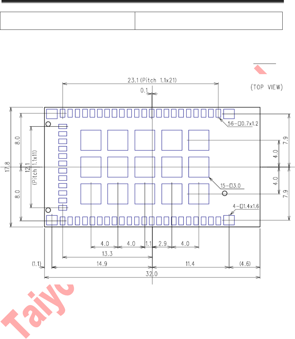
OUTLINE
Unit: mm, Tolerances unless otherwise specified: +/-0.2mm
26-Feb.-2014 Ver0.3
TAIYO YUDEN
TAIYO YUDEN 23/26
GT WYSAAVKXY
Control No.
HD-AD-A131203 (2/2)
Control name
Circuit Schematic
Module Pad Dimension
Unit:mm
(TOP VIEW)
1
24
25 48
49
60
61 6362 64 65
66 6867 69 70
71 7372 74 75
26-Feb.-2014 Ver0.3
TAIYO YUDEN
TAIYO YUDEN 24/26
GT WYSAAVKXY
Control No.
HD-BA-A131203 (1/2)
Control name
Pin Layout
No. Pin Name I/O Type
Pwr Domain Description 88MC200
GPIO Pin No.
1 GND P Ground GND - -
2 JTAG_TDO O - VIO_0 TDO for JTAG GPIO_20
3 JTAG_TCK O - VIO_0 TCK for JTAG GPIO_21
4 JTAG_TMS I/O - VIO_0 TMS for JTAG GPIO_22
5 JTAG_TDI I - VIO_0 TDI for JTAG GPIO_23
6 JTAG_TRST I - VIO_0 TRSTn for JTAG GPIO_24
7 RESETn I - VIO_0 Active low chip reset -
8 RSVD - - - No connect. Should be left open. -
9 M_WAKEUP I - VIO_0 Wake up signal GPIO_26
10 RSVD - - - No connect. Should be left open. -
11 ACOMP_GPIO_OUT O - VIO_1 ACOMP output synchronous or asynchronous level signals GPIO_29
12 ACOMP_EDGE_PULSE O - VIO_1 Output pulse aligned with Synchronized comparison result GPIO_30
13 SSP0_CLK I/O - VIO_1 Clock for SSP0 GPIO_32
14 SSP0_FRM I/O - VIO_1 Frame for SSP0 GPIO_33
15 SSP0_RXD I - VIO_1 RXD for SSP0 GPIO_34
16 SSP0_TXD O - VIO_1 TXD for SSP0 GPIO_35
17 SSP2_CLK I/O - VIO_1 Clock for SSP2 GPIO_40
18 SSP2_FRM I/O - VIO_1 Frame for SSP2 GPIO_41
19 SSP2_RXD I - VIO_1 RXD for SSP2 GPIO_42
20 SSP2_TXD O - VIO_1 TXD for SSP2 GPIO_43
21 SDIO_LED O - VIO_1 LED for SDIO GPIO_50
22 RSVD - - - No connect. Should be left open. -
23 GND P Ground GND - -
24 N.C. - - - No connect. Should be left open. -
25 N.C. - - - No connect. Should be left open. -
26 GND P Ground GND - -
27 N.C. - - - No connect. Should be left open. -
28 GND P Ground GND - -
29 RSVD - - - No connect. Should be left open. -
30 RSVD - - - No connect. Should be left open. -
31 USB_VBUS
I/O Power
- VBUS selection input in device mode; unused in host mode;
input/output for OTG mode to supply +5V@10mA during
session negotiation
-
32 USB_ID I - - USB OTG IDPIN pad -
33 USB_DP I/O - - USB D+ pad GPIO_57
34 USB_DM I/O - - USB D- pad GPIO_58
35 VIO_0 I Power VIO_0 IO power -
36 VIO_1 I Power VIO_1 IO power -
37 VIO_2 I Power VIO_2 IO power -
38 RSVD - - - No connect. Should be left open. -
39 V33I I Power V33I 3.3V power supply -
26-Feb.-2014 Ver0.3
TAIYO YUDEN
TAIYO YUDEN 25/26
GT WYSAAVKXY
Control No.
HD-BA-A131203 (2/2)
Control name
Pin Layout
No. Pin Name I/O Type
Pwr Domain Description 88MC200
GPIO Pin No.
40 GND P Ground GND - -
41 I2C0_SCL I/O - VIO_1 SCL for I2C0 GPIO_45
42 I2C0_SDA I/O - VIO_1 SDA for I2C0 GPIO_44
43 UART1_CTSn I - VIO_2 CTSn for UART1 GPIO_59
44 UART1_RTSn O - VIO_2 RTSn for UART1 GPIO_60
45 UART1_TXD O - VIO_2 TXD for UART1 GPIO_61
46 UART1_RXD I - VIO_2 RXD for UART1 GPIO_62
47 GND P Ground GND - -
48 GND P Ground GND - -
49 UART0_TXD O - VIO_2 TXD for UART0 GPIO_74
50 UART0_RXD I - VIO_2 RXD for UART0 GPIO_75
51 ADC_5 I/O - VIO_0 ADC channel 5 or Analog comparator Channel 5 GPIO_2
52 ADC_4 I/O - VIO_0 ADC channel 4 or Analog comparator Channel 4 GPIO_3
53 ADC_3_DAC I/O - VIO_0 ADC channel 3 or Analog comparator Channel 3 or DA Ref
or ADC Vref or DAC output GPIO_4
54 ADC_2 I/O - VIO_0 ADC channel 2 or Analog comparator Channel 2 GPIO_5
55 ADC_1 I/O - VIO_0 ADC channel 1 or Analog comparator Channel 1 GPIO_6
56 ADC_0 I/O - VIO_0 ADC channel 0 or Analog comparator Channel 0 GPIO_7
57 I2C1_SDA I/O - VIO_0 SDA for I2C1 GPIO_8
58 I2C1_SCL I/O - VIO_0 SCL for I2C1 GPIO_9
59 I2C2_SDA I/O - VIO_0 SDA for I2C2 GPIO_10
60 I2C2_SCL I/O - VIO_0 SCL for I2C2 GPIO_11
61 GND P Ground GND - -
62 GND P Ground GND - -
63 GND P Ground GND - -
64 GND P Ground GND - -
65 GND P Ground GND - -
66 GND P Ground GND - -
67 GND P Ground GND - -
68 GND P Ground GND - -
69 GND P Ground GND - -
70 GND P Ground GND - -
71 GND P Ground GND - -
72 GND P Ground GND - -
73 GND P Ground GND - -
74 GND P Ground GND - -
75 GND P Ground GND - -
26-Feb.-2014 Ver0.3
TAIYO YUDEN
TAIYO YUDEN 26/26
GT WYSAAVKXY
Control No.
(1/1)
Control name
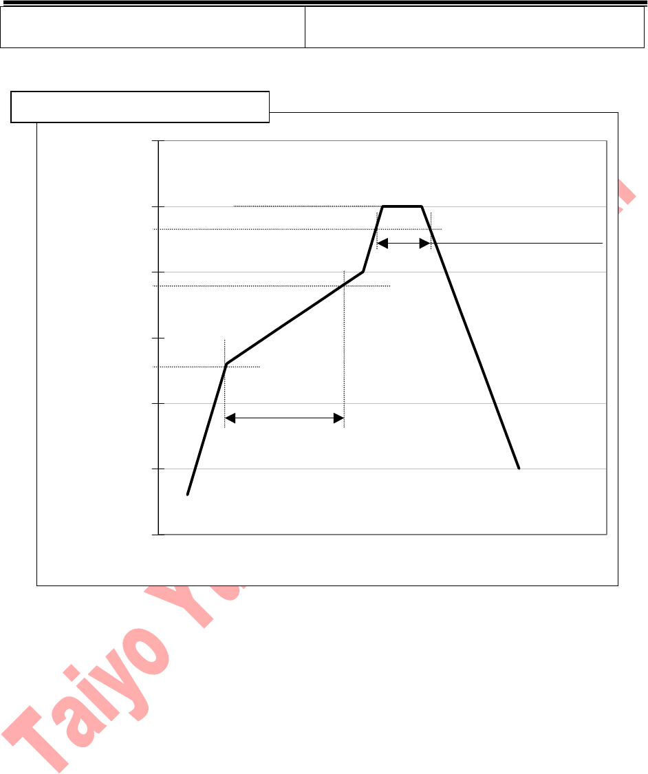
Reflow profile
0
50
100
150
200
250
300
IN OUT
Temp(deg)
130-180deg Pre-heat
: 60~120sec
Peak Temp:250deg Max
230deg up : 40secMax
Recommented Reflow Profile