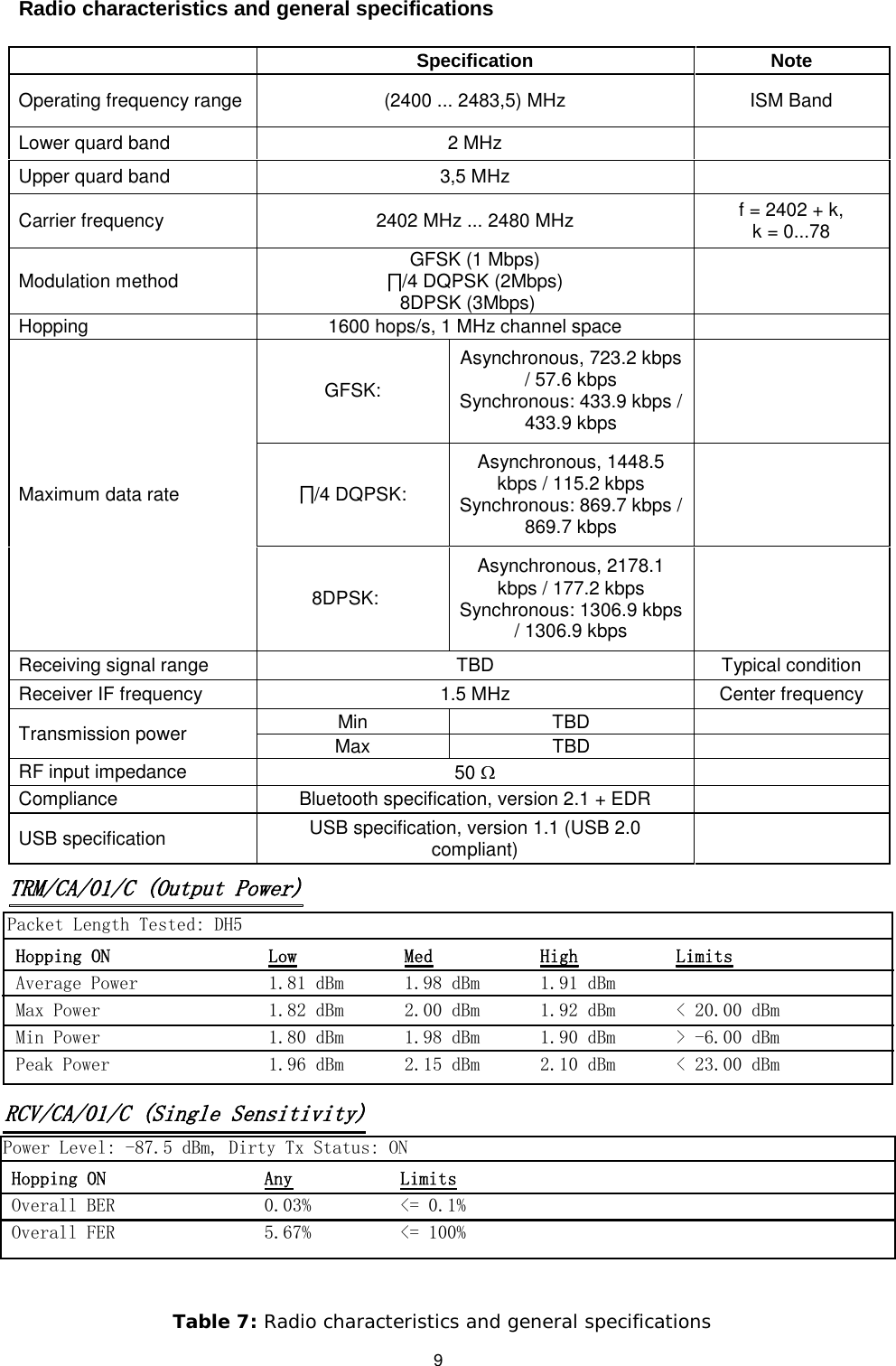
TCL Technoly Electronics PS000015 Bluetooth Module User Manual Product Data Sheet

TCL Technoly Electronics (Huizhou) Co., Ltd. Bluetooth Module Product Data Sheet

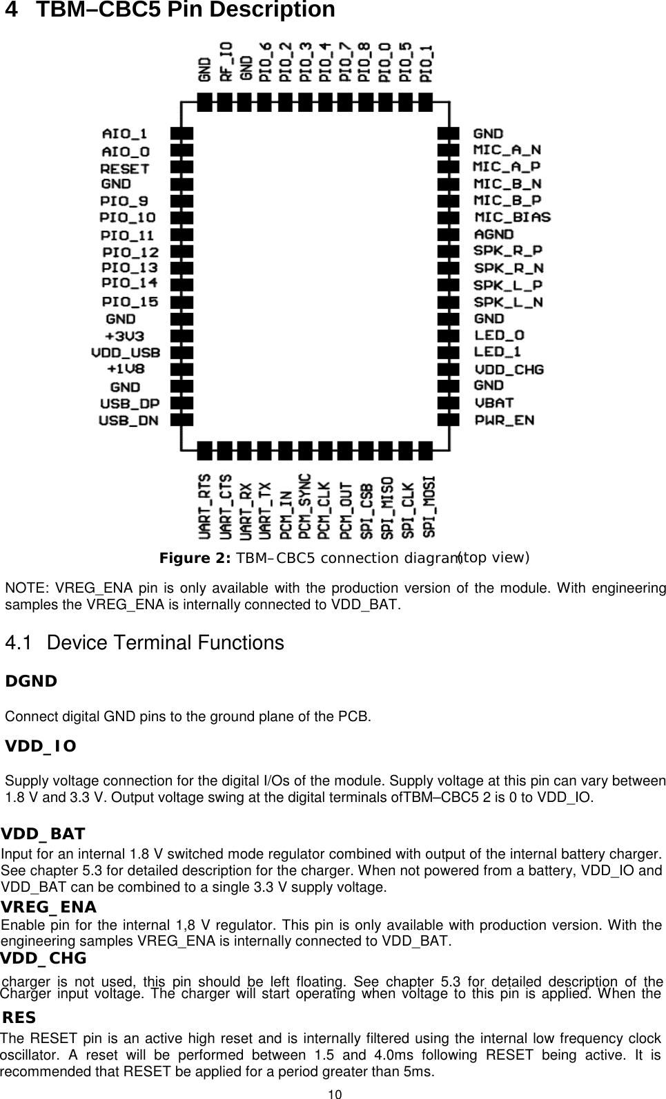
TBM-CBC5_User Manual_Rev4

                      TBM-CBC5 DATA SHEET Monday, 29 September 2014  Version 1.1  Datasheet by Peter.huangTONLY
1 Correct 8DQPSK to 8DPSK2014 29 121 10                                        Revision History  Date  Version Description  Author 2013- - V1.0  n  First Release         -09-    V1. n
  2 TBM–CBC5Bluetooth Audio Module   DESCRIPTION: TBM–CBC5 is first generation of TCL Bluetooth modules.It provides highest level of integration with integrated 2.4GHz radio, DSP, battery charger, stereo codec mono and ,stereo audio applications.TBM–CBC5 is alsoready to support the lates Bluetooth 3.0 standard The embedded DSP core allows enhancement of the product with features such as advanced audio decoding (MP3, AAC, AAC+), echo cancellation, noise reduction, and data manipulation. TCL’s TONLY flexible  firmware enables device manufacturers to easily add wireless, secure, and standard-based Bluetooth connectivity into new or existing applications with very limited development and  manufacturing effort.   APPLICATIONS: • High quality wireless stereo headsets • Wireless mono headsets • Wireless speakers • USB multimedia dongles • MP3 players • VoIP handsets • Hands-free car kits  FEATURES: • TBM–CBC5 Bluetooth module Solution For mono and Stereo Audio Solutions • Integrated DSP, Stereo Codec, and Battery Charger   • Bluetooth 3.0 + EDR Compliant   • Class 2 - Range up to 30 Meters • Temperature range from  -30C to +85C • Low Power Consumption • TCL TONLY Firmware for Controlling Connections and Configuring Settings • Supported Bluetooth Profiles: A2DP, AVRCP, HFP, HFP-AG, SPP, OPP, FTP, HSP, DUN, PBAP and HID ect...      Size: 13.5*21 mm40-BTP518HFD4G
  3 2  Block Diagram and Descriptions  RAMBaseband DSPMCUKalimba DSP2.4 GHz RadioI/OBC05-MMXTAL FlashUART/USB PIOAudio In/OutPCM/I2S/SPDIFSPIReset circuitry  Figure 1: Block diagram of TBM–CBC5 BC05-MM The BlueCore05-MM is a single-chip radio and baseband IC for Bluetooth 2.4GHz systems. It provides a fully compliant Bluetooth system to v3.0+EDR of the specification for data and voice.   BlueCore05-MM contains the Kalimba DSP co-processor with double the MIPS of BlueCore03-MM, supporting enhanced audio applications. BlueCore05-MM integrates a 16-bit stereo codec and it has a fully differential audio interface with a low noise microphone bias.  Crystal The crystal oscillates at 26MHz. Flash Flash memory is used for storing the Bluetooth protocol stack and Virtual Machine applications. It can also be used as an optional external RAM for memory-intensive applications. Balanced Filter Combined balun and filter changes the balanced input/output signal of the module to unbalanced signal of the antenna. The filter is a band pass filter (ISM band). Antenna TBM–CBC5 uses ceramic chip antenna with high dielectric constant, which makes the antenna very insensitive to surrounding environment and thus gives high design freedom around the antenna.  USB The USB interface is a full speed Universal Serial Bus (USB) interface for communicating with other compatible digital devices.TBM–CBC5 acts as a USB peripheral, responding to requests from a Master host controller such as a Personal Computer (PC).
  4 Synchronous Serial Interface This interface is a synchronous serial port interface (SPI) for interfacing with other digital devices. The SPI port can be used for system debugging. It can also be used for programming the Flash memory. UART This interface is a standard Universal Asynchronous Receiver Transmitter (UART) interface for communicating with other serial devices. PCM / I2S / SPDIF Interface This interface is a bi-directional serial programmable audio interface supporting PCM, I2S and SPDIF formats. Audio Interface The audio interface of TBM–CBC5 has fully differential inputs and outputs and a microphone bias output. A high-quality stereo audio Bluetooth application can be implemented with minimum amount of external components.  Programmable I/O BTP518B has a total of 10 digital programmable I/O terminals. These are controlled by the firmware running on the device. Reset TBM–CBC5 has a reset circuitry that is used to reset the module in the startup to ensure proper operation of the flash memory. Alternatively, the reset can be externally driven by using a TBM–CBC5 reset pin. 802.11 Coexistence Interface Dedicated hardware is provided to implement a variety of coexistence schemes. Channel skipping AFH (Adaptive Frequency Hopping), priority signaling, channel signaling, and host passing of channel instructions are all supported. The features are configured in firmware. Since the details of some methods are proprietary (e.g. Intel WCS)
  5 3  Electrical Characteristics Absolute maximum ratings              Min Max Unit Storage temperature  -40 85  °C Operating temperature  -30  85  °C VDD_IO  -0.4 3.6  V VDD_BAT   -0.4 4.4   V VDD_CHG   -0.4 6.5   V Terminal voltages  -0.4 Vdd + 0,4  V        The module should not continuously run under these conditions. Exposure to absolute maximum rating conditions for extended periods of time may affect reliability and cause permanent damage to the device. Table 1: Absolute maximum ratings  Recommended operating conditions           Min Max Unit Operating temperature  -40 85 °C VDD_IO 1.7 3.6  V VDD_BAT 2.5 4.4  V VDD_CHG  0  6.5  V Terminal voltages  0  VDD  V Table 2: Recommended operating conditions
  6  Terminal characteristics             Min Typ Max Unit I/O voltage levels            VIL input logic level low  -0.4  -  0.25xVDD  V VIH input logic level high 0.625xVDD  -  Vdd + 0.3  V VOL output logic level low  0  -  0.125  V VOH output logic level high 0.75xVDD  -  VDD  V Reset terminal            VTH,res threshold voltage 0.64 0.85 1.5  V RIRES input resistance     220     kΩ CIRES input capacitance     220     nF Input and tri-state current with            Strong pull-up  -100  -40  -10 µΑ Strong pull-down 10 40 100 µΑ Weak pull-up  -5  -1  -0.2 µΑ Weak pull-down 0.2  1  5  µΑ I/O pad leakage current  -1  0  1  µΑ LED driver pad            Off current  -  1  2  µΑ On resistance (VPAD < 0.5 V)  -  20 33 Ω On resistance, pad enabled by battery charger (VPAD < 0.5 V) -  20 50 Ω Table 3: Terminal characteristics
  7  Battery charger            Battery charger     Min Typ Max Unit VDD_CHG     4.5  -  6.5  V Charging mode (VDD_BAT rising to 4.2 V) Supply current (a)  -  4.5  6  mA Battery trickle charge current (b) (c) Maximum setting  -  14  -  mA Minimum setting  -  4  -  mA Maximum battery fast charge current (d) (c) Headroom > 0.7 V (e)  -  140  -  mA Headroom = 0.3 V  -  120  -  mA Minimum battery fast charge current (d) (c) Headroom > 0.7 V  -  40  -  mA Headroom = 0.3 V  -  35  -  mA Trickle charge voltage threshold  -  2.9  -  V Float voltage (with correct trim value set), VFLOAT(f) 4.17 4.2 4.23  V Float voltage trim step size (f)  -  50  -  mV Battery charge termination current, as a percentage of the fast charge current 5  10 20  % Standby Mode (BAT_P falling from 4.2V) Supply current (a)  -  1.5  2  mA Battery current  -  -5  -  μA Battery recharge hysteresis (g) 100 - 200 mV Shutdown Mode (VDD_CHG too low or disabled by firmware) VDD_CHG under-voltage threshold VDD_CHG rising  -  3.9  -  V VDD_CHG falling  -  3.7  -  V VDD_CHG - BAT_P lockout threshold VDD_CHG rising  -  0.22  -  V VDD_CHG falling  -  0.17  -  V Supply current  -  1.5  2  mA Battery current  -1  -  0  μA                       (a) Current into VDD_CHG - does not include current delivered to battery (I VDD_CHG - I BAT_P) (b) BAT_P < Float voltage (c) Charge current can be set in 16 equally spaced steps (d) Trickle charge threshold < BAT_P < Float voltage (e) Where headroom = VDD_CHG - BAT_P (f) Float voltage can be adjusted in 15 steps. Trim setting is determined in production test and must be loaded into the battery charger by firmware during boot-up sequence (g) Hysteresis of (VFLOAT - BAT_P) for charging to restart Table 4: Battery charger characteristics
  8  Stereo CODEC Analogue to Digital Converter Parameter Conditions Min Typ Max Unit Resolution     -  -  16 Bits Input Sample Rate, Fsample    8  -  44.1 kHz Signal to Noise Ratio, SNR fin = 1kHz B/W = 20Hz→20kHz A-Weighted THD+N < 1% 150mVpk-pk input Fsample    8 kHz  -  82  -  dB 11.025 kHz  -  81  -  dB 16 kHz  -  80  -  dB 22.050 kHz  -  79  -  dB 32 kHz  -  79  -  dB 44.1 kHz  -  78  -  dB Digital Gain Digital Gain Resolution = 1/32dB  -24  -  21.5 dB Analogue Gain Analogue Gain Resolution = 3dB  -3  -  42 dB Input full scale at maximum gain (differential)  -  4  -  mV rms Input full scale at minimum gain (differential)  -  800  -  mV rms 3dB Bandwidth  -  20  -  kHz Microphone mode input impedance  -  6.0  -  kΩ THD+N (microphone input) @ 30mV rms input  -  0.04  -  % Table 5: Stereo CODEC ADC characteristics  Stereo CODEC Digital to Analog Converter Parameter Conditions Min Typ Max Unit Resolution     -  -  16 Bits Input Sample Rate, Fsample    8  -  48 kHz Signal to Noise Ratio, SNR fin = 1kHz B/W = 20Hz→20kHz A-Weighted THD+N < 1% 150mVpk-pk input Fsample    8 kHz  -  95   -  dB 11.025 kHz  -  95   -  dB 16 kHz  -  95   -  dB 22.050 kHz  -  95   -  dB 32 kHz  -  95   -  dB 44.1 kHz  -  95   -  dB Digital Gain Digital Gain Resolution = 1/32dB  -24  -  21.5 dB Analogue Gain Analogue Gain Resolution = 3dB  0  -  -21 dB Output voltage full scale swing (differential)  -  750  -  mV rms Allowed Load Resistive 16(8)  -  OC Ω Capacitive  -  -  500 pF THD+N 100kΩ load  -  -  0.01  % THD+N 16Ω load  -  -  0.1  % SNR (Load = 16Ω, 0dBFS input relative to digital silence)  -  95  -  dB Table 6: Stereo CODEC DAC characteristics
8DPSK:8DPSK (3Mbps)  9  Radio characteristics and general specifications           Specification Note Operating frequency range (2400 ... 2483,5) MHz ISM Band Lower quard band 2 MHz    Upper quard band 3,5 MHz    Carrier frequency 2402 MHz ... 2480 MHz f = 2402 + k,  k = 0...78 Modulation method GFSK (1 Mbps) ∏/4 DQPSK (2Mbps)     Hopping 1600 hops/s, 1 MHz channel space    Maximum data rate GFSK: Asynchronous, 723.2 kbps / 57.6 kbps Synchronous: 433.9 kbps / 433.9 kbps   ∏/4 DQPSK: Asynchronous, 1448.5 kbps / 115.2 kbps Synchronous: 869.7 kbps / 869.7 kbps    Asynchronous, 2178.1 kbps / 177.2 kbps Synchronous: 1306.9 kbps / 1306.9 kbps   Receiving signal range TBD Typical condition Receiver IF frequency 1.5 MHz  Center frequency Transmission power Min TBD    Max TBD    RF input impedance 50 Ω   Compliance Bluetooth specification, version 2.1 + EDR    USB specification USB specification, version 1.1 (USB 2.0 compliant)   Table 7: Radio characteristics and general specifications     RCV/CA/01/C (Single Sensitivity) Power Level: -87.5 dBm, Dirty Tx Status: ON Hopping ONOverall BEROverall FERAny0.03%5.67%Limits<= 0.1%<= 100% TRM/CA/01/C (Output Power) Packet Length Tested: DH5 Hopping ONAverage PowerMax PowerMin PowerPeak PowerLow1.81 dBm1.82 dBm1.80 dBm1.96 dBmMed1.98 dBm2.00 dBm1.98 dBm2.15 dBmHigh1.91 dBm1.92 dBm1.90 dBm2.10 dBmLimits󳴆< 20.00 dBm> -6.00 dBm< 23.00 dBm
  10 4  TBM–CBC5 Pin Description Figure 2: TBM–CBC5 connection diagram (top view)  NOTE: VREG_ENA pin is only available with the production version of the module. With engineering samples the VREG_ENA is internally connected to VDD_BAT. 4.1 Device Terminal Functions DGND  Connect digital GND pins to the ground plane of the PCB. VDD_IO Supply voltage connection for the digital I/Os of the module. Supply voltage at this pin can vary between 1.8 V and 3.3 V. Output voltage swing at the digital terminals ofTBM–CBC5 2 is 0 to VDD_IO.  VDD_BAT Input for an internal 1.8 V switched mode regulator combined with output of the internal battery charger. See chapter 5.3 for detailed description for the charger. When not powered from a battery, VDD_IO and VDD_BAT can be combined to a single 3.3 V supply voltage.  VREG_ENA Enable pin for the internal 1,8 V regulator. This pin is only available with production version. With the engineering samples VREG_ENA is internally connected to VDD_BAT.  VDD_CHG  Charger input voltage. The charger will start operating when voltage to this pin is applied. When the charger is not used, this pin should be left floating. See chapter 5.3 for detailed description of the  RES  The RESET pin is an active high reset and is internally filtered using the internal low frequency clock oscillator. A reset will be performed between 1.5 and 4.0ms following RESET being active. It is recommended that RESET be applied for a period greater than 5ms.
  11 PIO0 – PIO15 Programmable digital I/O lines. All PIO lines can be configured through software to have either weak or strong pull-ups or pull-downs. Configuration for each PIO line depends on the application. See section 16 “I/O parallel ports” for detailed descriptions for each terminal. Default conf iguration for all of the PIO lines is input with weak internal pull-up.    AIO0 – AIO1  AIOs can be used to monitor analogue voltages such as a temperature sensor for the battery charger. AIOs can also be configured to be used as digital I/Os. The voltage level at these pins is 0 V to 1,5 V. UART_NRTS A CMOS output with a weak internal pull-up. This pin can be used to implement RS232 hardware flow control where RTS (request to send) is an active low indicator. The UART interface requires an external RS232 transceiver chip. UART_NCTS A CMOS input with a weak internal pull-down. This pin can be used to implement RS232 hardware flow control where CTS (clear to send) is an active low indicator. The UART interface requires an external RS232 transceiver chip. UART_RXD A CMOS input with a weak internal pull-down. RXD is used to implement UART data transfer from another device to TBM–CBC5.The UART interface requires an external RS232 transceiver chip. UART_TXD A CMOS output with a weak internal pull-up. TXD is used to implement UART data transfer from T BM–CBC5to another device. The UART interface requires external RS232 transceiver chip.
  12 PCM_OUT A CMOS output with a weak internal pull-down. Used in the PCM (pulse code modulation) interface to transmit digitized audio. The PCM interface is shared with the I2S interface. PCM_IN  A CMOS input with a weak internal pull-down. Used in the PCM interface to receive digitized audio. The PCM interface is shared with the I2S interface. PCM_CLK A bi-directional synchronous data clock signal pin with a weak internal pull-down. PCMC is used in the PCM interface to transmit or receive the CLK signal. When configured as a master, WT32 generates the clock signal for the PCM interface. When configured as a slave, the PCMC is an input and receives the clock signal from another device. The PCM interface is shared with the I2S interface. PCM_SYNC A bi-directional synchronous data strobe with a weak internal pull-down. When configured as a master, TBM–CBC5  generates the SYNC signal for the PCM interface. When configured as a slave, the PCMS isan input and receives the SYNC signal from another device.The PCM interface is shared with the I2S interface. USB_D+ A bi-directional USB data line with a selectable internal 1.5 kΩ pull-up implemented as a current source (compliant with USB specification v1.2) An external series resistor is required to match the connection to the characteristic impedance of the USB cable. USB_D- A bi -directional USB data line. An external series resistor is required to match the connection to the characteristic impedance of the USB cable. SPI_NCSB A CMOS input with a weak internal pull-down. Active low chip select for SPI (serial peripheral interface). SPI_CLK  A CMOS input for the SPI clock signal with a weak internal pull-down. TBM–CBC5  is the slave and receives the clock signal from the device operating as a master. SPI_MISO  An SPI data output with a weak internal pull-down.  SPI_MOSI  An SPI data input with a weak internal pull-down. RF  This pin can be used when not using a chip antenna or w.fl connector of the module. AUDIO_IN_P_RIGHT and AUDIO_IN_N_RIGHT
  13 Right channel audio inputs. This dual audio input can be configured to be either single-ended or fully differential and programmed for either microphone or line input. Route differential pairs close to each other and use a solid dedicated audio ground plane for the audio signals.  AUDIO_IN_P_LEFT and AUDIO_IN_N_LEFT Left channel audio input. ESD protection and layout considerations similar to right channel audio should be used. AUDIO_OUT_P_RIGHT and AUDIO_OUT_N_RIGHT Right channel audio output. The audio output lines should be routed differentially to either the speakers or to the output amplifier, depending on whether or not a single-ended signal is required. Use low impedance ground plane dedicated for the audio signals. AUDIO_OUT_P_LEFT and AUDIO_OUT_N_LEFT Left channel audio output. The same guidelines apply to this section as discussed previously. MIC_BIAS Bias voltage output for a microphone. Use the same layout guidelines as discussed previously with other audio signals.  LED0 TBM–CBC5  includes a pad dedicated to driving LED indicators. This terminal may be controlled by firmware and it can also be set by the battery charger. The terminal is an open-drain output, so the LED must be connected from a positive supply rail to the pad in series with a current limiting resistor. It is recommended that the LED pad is operated with a pad voltage below 0.5V. In this case, the pad can be thought of as a resistor, RON. The resistance together with the external series resistor will set the current, ILED, in the LED. Value for the external series resistance can be calculated from the Equation 1 ONLEDFLED RIVVDDR−−= Equation 1: LED series resistor Where VF is the forward voltage drop of the LED, ILED is the forward current of the LED and RON is the on resistance (typically 20 Ω) of the LED driver.
 5. TBM–CBC5 Physical DimensionsRecommended PCB land pattern for TBM–CBC514
Internal Photo Sony CorporationPersonal Audio System[Model : SRS-X3]
Internal Photo Sony CorporationPersonal Audio System[Model : SRS-X3]Antenna Antenna Type:PCB Layout Inverted-F Antenna;Gain:2.12dBi;
Internal Photo Sony CorporationPersonal Audio System[Model : SRS-X3]BTMain board photo
Internal Photo Sony CorporationPersonal Audio System[Model : SRS-X3]CN board photo
HowtofixedthemoduletoSRS‐X3.WhenthePCBAMainboard,CNboardandothersisOK.InsertFFCcableintoJackXP19onMainboard,insertthespeakercableintoJackXS1,XS2onMainboard,asfollowphoto:InsertNFCcableintoJackXP15onMainboard,andinserttheMainboardtoplasticcase,asfollowphoto
ConnecttheMainboardtocnboardwiththeFFCcable,insertthebatterycableintoJackXP1001ontheCNboard,inserttheMICcableintoJackXP589ontheMainboard,asfollowphoto;
Connectthespeakercabletospeakerandfixthespeakerontheplasticcase,asfollowphoto;FixtheFrontpanelontheplasticcase,asfollowphoto;
FixtheMIContheplasticcase,asfollowphoto;FixtheIronnetsontheplasticcase,asfollowphoto;
Fixthebottomcoverontheplasticcase,asfollowphoto;Now,oneofSRS‐X3isfixedOK,asfollowphoto;FrontView
BackView
  FCC Statement Changes or modifications not expressly approved by the party responsible for compliance could void the user's authority to operate the equipment    This device complies with Part 15 of the FCC Rules. Operation is subject to the following two conditions: (1) this device may not cause    harmful interference, and (2) this device must accept any interference received, including interference that may cause undesired operation.    IC Statement This device complies with Industry Canada licence-exempt RSS standard(s). Operation is subject to the following two conditions: (1) this device may not cause interference, and (2) this device must accept any interference, including interference that may cause undesired operation of the device. Le présent appareil est conforme aux CNR d'Industrie Canada applicables aux appareils radio exempts de licence. L'exploitation est autorisée aux deux conditions suivantes : (1) l'appareil ne doit pas produire de brouillage, et (2) l'utilisateur de l'appareil doit accepter tout brouillage radioélectrique subi, même si le brouillage est susceptible d'en compromettre le fonctionnement.   "Contains IC:9976A-PS000015".The end host device should bear the label which indicate""Contains FCC ID:ZVAPS000015".or

Navigation menu