TESSERA TECHNOLOGY 0002 WIRELESS UNIT User Manual USERS MANUAL
TESSERA TECHNOLOGY INC. WIRELESS UNIT USERS MANUAL
USERS MANUAL
MB-RF1146 User’s Manual
© TESSERA TECHNOLOGY INC.
Rev 1
2011/05/06
- 1 -
[NOTES]
The information in this document is subject to change without notice. No part of this
document may be copied or reproduced in any form or by any means without the prior
written consent of TESSERA TECHNOLOGY INC.
TESSERA TECHNOLOGY INC. assumes no liability for infringement of patents or
copyrights of third parties by or arising from use of a product described herein.
This product is designed and manufactured with intention for use in evaluation and
prototyping by engineers with knowledge of security, safety and reliability. TESSERA
TECHNOLOGY INC. would like to inform, that the standard quality assurance procedure(s)
have not been fully applied to this product and its documentation and that TESSERA
TECHNOLOGY INC. cannot assure the full and error free function and/or the standard
quality level.
[CAUTION]
This equipment should be handled like a CMOS semiconductor device. The user must take
all precautions to avoid build-up of static electricity while working with this equipment. All test
and measurement tool including the workbench must be grounded. The user/operator must
be grounded using the wrist strap. The connectors and/or device pins should not be touched
with bare hands.
- 2 -

[FCC WARNING & NOTICE]
●Changes or modifications not expressly approved by the party responsible for compliance
could void the user’s authority to operate the equipment.
Class B:
This equipment has been tested and found to comply with the limits for a Class B digital
device, pursuant to part 15 of the FCC Rules. These limits are designed to provide
reasonable protection against harmful interference in a residential installation. This
equipment generates, uses and can radiate radio frequency energy and, if not installed and
used in accordance with the instructions, may cause harmful interference to radio
communications. However, there is no guarantee that interference will not occur in a
particular installation. If this equipment does cause harmful interference to radio or television
reception, which can be determined by turning the equipment off and on, the user is
encouraged to try to correct the interference by one or more of the following measures:
● Reorient or relocate the receiving antenna.
● Increase the separation between the equipment and receiver.
● Connect the equipment into an outlet on a circuit different from that to which the receiver is
connected.
● Consult the dealer or an experienced radio/TV technician for help.
This device complies with Part 15 of the FCC Rules. Operation is subject to the following
two conditions:
●this device may not cause harmful interference, and
●this device must accept any interference received, including interference that may cause
undesired operation.
●The host device shall also comply with the certification labeling requirements of each of the
modules it contains.
●A reference to the enclosed module displaying its FCC ID certification number.
Recommended wording:
Contains FCC ID: X8U0002
- 3 -
Contents
1. Hardware Specifications ................................................................................................5
2. Layout of hardware functions......................................................................................... 5
3. Hardware functions........................................................................................................6
3.1. J1 (Connector) ...................................................................................................... 6
3.2. CN1,CN2 (Connector)...........................................................................................6
3.3. EVDD (Solder short pad) ......................................................................................7
3.4. RF (Solder short pad)............................................................................................ 7
4. RF test procedure..........................................................................................................8
5. Circuit diagram ............................................................................................................ 17
- 4 -
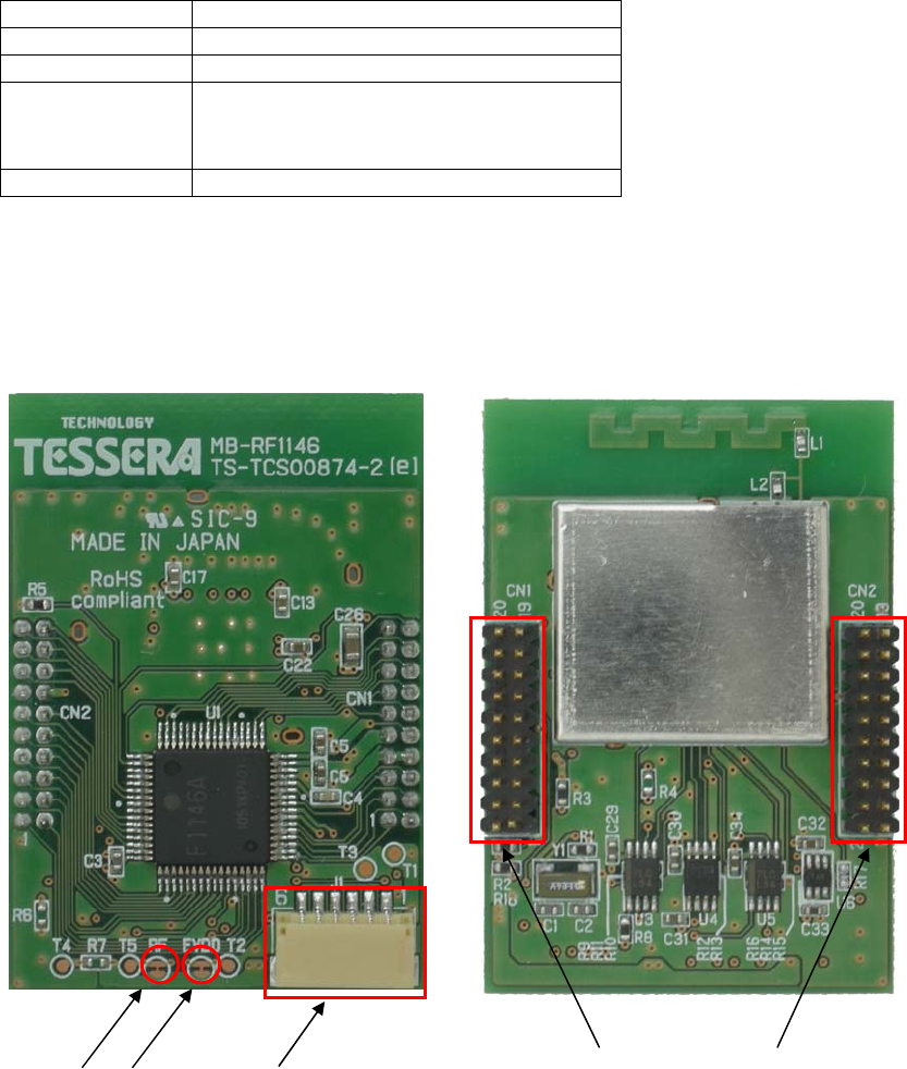
1. Hardware Specifications
Supply voltage DC3.0V
Microcontroller uPD78F1146AGA-HAB-AX
RF IC UZ2400.D
Clock
Main clock
: 16MHz (UZ2400.D CLK_OUT)
Sub clock : 32.768KHz
Dimension 32x25 (HxW mm)
2. Layout of hardware functions
CN2
CN1
J1
RF EVDD
- 5 -

3. Hardware functions
3.1. J1 (Connector)
Interface connector for universal use.
(JST SM06B-SRSS-TB(LF)(SN))
Pin No. Signal name
1 EVDD
2 GND
3 P10/SCK00
4 P11/SI00/RxD0
5 P12/SO00/TxD0
6 P141/PCLBUZ1/INTP7
3.2. CN1,CN2 (Connector)
Interface connector for universal use.
(FCI 20021111-00020T4LF)
CN1 connection
Pin No. Signal name
1 P120/INTP0/EXLVI
2 P42/TI04/TO04
3 P41/TOOL1
4 P40/TOOL0
5 RESET
6 FLMD0
7 GND
8 GND
9 VDD
10 EVDD
11 P60/SCL0
12 P61/SDA0
13 P77/KR7/INTP11
14 P76/KR6/INTP10
15 P75/KR5/INTP9
16 P74/KR4/INTP8
17 P06/TI06/TO06
18 P05/TI05/TO05
19 RF Power
20 P50/INTP1
CN2 connection
Pin No. Signal name
1 P140/PCLBUZ0/INTP6
2 P141/PCLBUZ1/INTP7
3 P00/TI00
4 P01/TO00
- 6 -
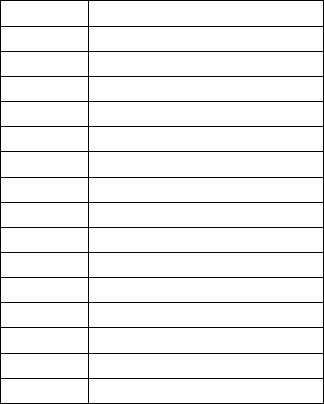
5 P20/ANI0
6 P21/ANI1
7 P22/ANI2
8 P23/ANI3
9 P24/ANI4
10 P25/ANI5
11 P26/ANI6
12 P27/ANI7
13 AVSS
14 AVREF
15 P10/SCK00
16 P11/SI00/RxD0
17 P12/SO00/TxD0
18 P13/TxD3
19 P14/RxD3
20 P17/TI02/TO02
Power and GND were respectively connected internally at default setting.
3.3. EVDD (Solder short pad)
This Solder short pad connects VDD and EVDD at original setting.
You can separate VDD and EVDD with cutting the dent part.
3.4. RF (Solder short pad)
This Solder short pad connects VDD and RF power at original setting.
You can separate VDD and RF power with cutting the dent part.
- 7 -
4. RF test procedure
Procedure for one to one transmit/receive test
Assumption here in this section is, you have two boards, in one of which the execution code
for the “RF_TEST” was programmed by the debugger. You also prepare two PCs or one PC
with more than one usb interface.
We will use the board you have program with the short address 0x0001 as a transmitter. We
now learn how to prepare an executable program for receiver side, which may be assigned
a short address of 0x0002.
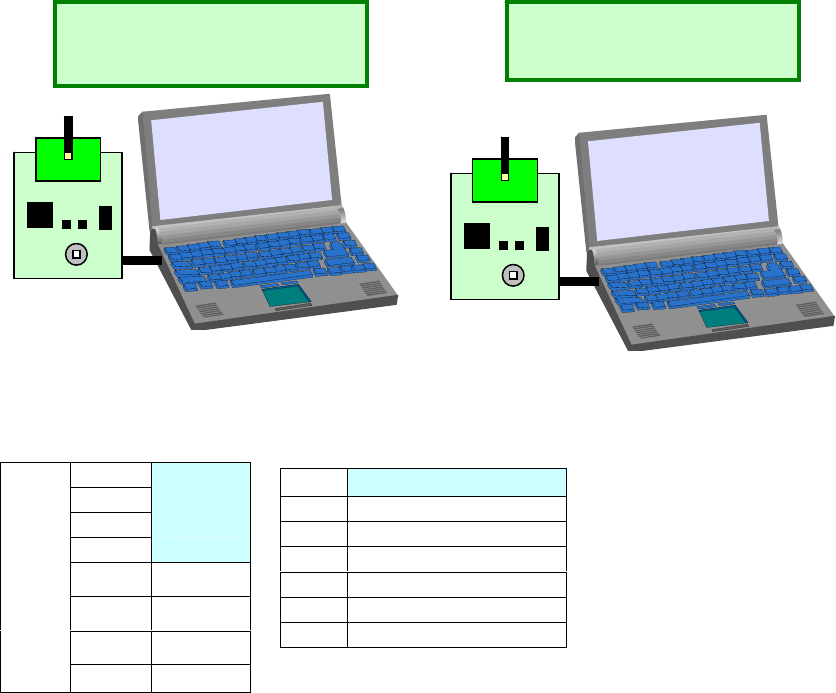
4.1. Settings for a receiver
the board setting is configured as follows as a receiver.
Bit1
Bit2
Bit3
Bit4
ALL
OFF
Bit5 ON
Bit6 ON
Bit7 OFF
SW4
Bit8 OFF
SW6 「K0R-K0USB」
SW5 3.0V
JP3 1-2 Short(USB)
JP5 Any
JP2 1-2 Short (Regulator)
JP1 Short
JP4 Short
Transmitte
r
Short address : 0001
Receive
r
Short address : 0002
Connect the board with a PC by a USB cable, then you will find the Power LED lit on the
board.
- 8 -
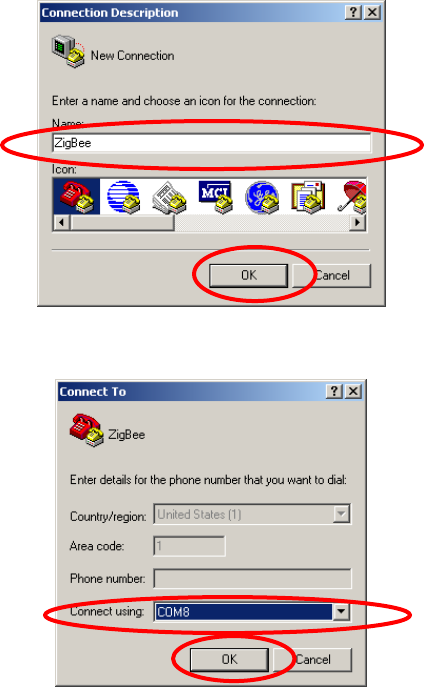
Then, we need a hyperterminal on the PC.
On MS-Windows in your PC, please select [All Programs] -> [Accessory] ->
[Communication] -> [HyperTerminal]
You may assign your favorite name on a connection. Then, click OK.
You need to learn the COM port number you connected the USB cable. If you don’t know the
com port number, please find it at [Control Panel] [System] [Hardware] [Device
Manager] [Port (COM and LPT)].
- 9 -
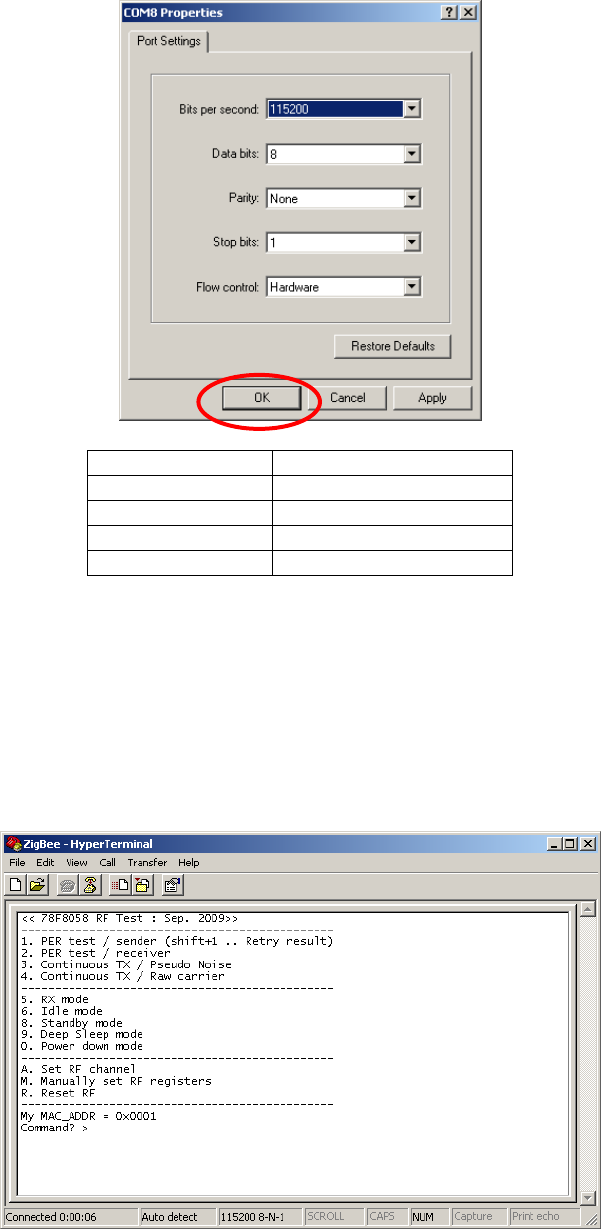
Bits per second 115200
Data bits 8
Parity None
Stop bits 1
Flow control None
(Property -> Setting -> ASCII)
Local Echo OFF
No Line Feed
Please set the COM port at 115200 bps, 8 data bits, no parity, 1 stop bit, and no flow control.
Then, please click “OK”.
Then, please reset the receiver board by pressing the SW7.
Now you will find the following opening menu in the window.
- 10 -

Please select “2” from the MENU to start the board as a receiver.
Command? >2 (PER test/reciever)
[My Profile]
-------------------------------------
MAC : 22:95:00:02:00:00:00:47
Short : 0002
PanID : 2514
-------------------------------------
[Set channel to 11 (Cmd)]
If you see the display as shown above, the receiver set-up has been completed.
- 11 -
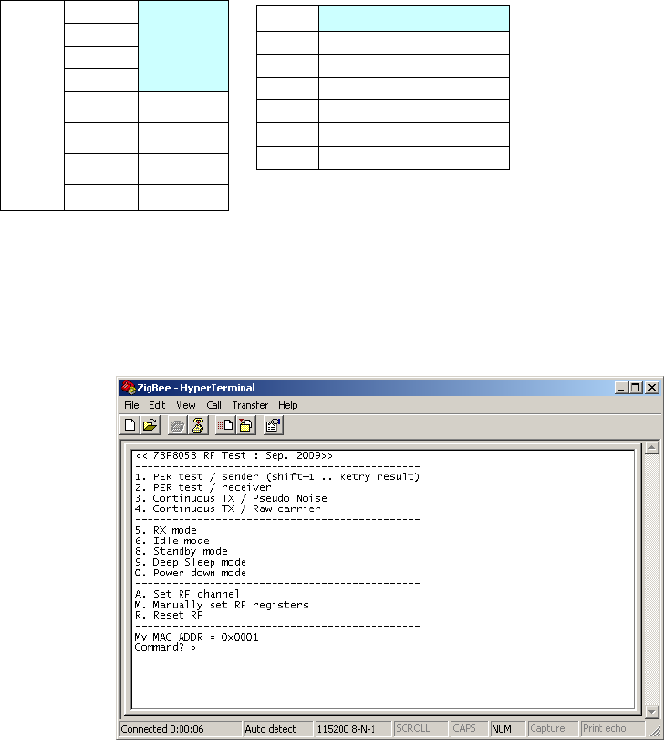
4.2. Settings for a transmitter
Please configure the board of a transmitter as follows,
Bit1
Bit2
Bit3
Bit4
ALL
OFF
Bit5 ON
Bit6 ON
Bit7 OFF
SW4
Bit8 OFF
SW6 「K0R-K0USB」
SW5 3.0V
JP3 1-2 short(USB)
JP5 Any
JP2 1-2 short(Regulator)
JP1 Short
JP4 Short
Please connect the transmitter board to a PC. Please confirm the LED lit on the board.
Please start-up a hyperterminal for a transmitter.
Please reset the transmitter board by pressing the SW7.
Now you will find the following opening menu in the window.
- 12 -
Please select the command “1” to start the Packet Error Rate test.
Command? >1 (PER test/sender)
[My Profile]
-------------------------------------
MAC : 22:95:00:01:00:00:00:47
Short : 0001
PanID : 2514
-------------------------------------
Send to (Short addr) ? :
If you see “Send to (Short addr) ? :”, please input the receiver address of 0002.
Then, you will be asked how many packets you wish to consume in the PER test.
You may input “1000”.
Then, you will be asked the interval of packets in msec.
You may input 3 msec.
Then, the PER test will be executed.
You will see,
Sent: The number of packets sent.
Received: The number of the received packets.
PER: The calculated PER in %.
RSSI: The maximum and minimum RSSI values in the PER test
[Note]
PER= Packet Error Rate
RSSI= Received Signal Strength Indication
-------------------------------------
Send to (Short addr) ? : 2
Send count (dec) ? : 1000
Interval (dec/msec) ? : 3
[Set channel to 11 (Cmd)]
Prepare to send..OK
[Set channel to 11 (Current)]
Request to result..OK
[Results]
-------------------------------------
From : 0001
To : 0002
-------------------------------------
Sent : 1000
Recieved : 1000
PER : 0.0000%
RSSI : max FF / min D0
-------------------------------------
Press any key to the menu
- 13 -
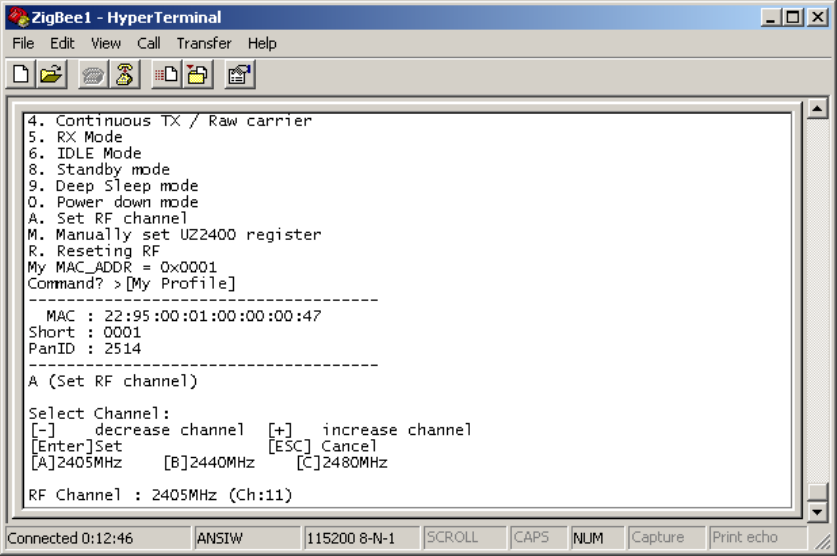
4.3. Channel setting
In the previous example, you may have also found the RF channel used in this test is the
Channel 11. The channel is specified by the IEEE 802.15.4 specification.
The channel 11 is assigned at 2405 MHz. You can change the channel in the PER test in
5MHz step to the maximum channel of 26th at 2480 MHz.
To do it, please press “A” in the command prompt. Then, please choose the channel by [+],
[-], [A], [B], or [C]. In the example below, the channel 23th, 2465 MHz, was selected.
- 14 -
To execute the PER test at the channel 23, press [Enter] in your keyboard, then,
choose “1” to initiate the PER test mode. Then, you may input 1000 packet in 5 msec
interval to see the following example. Please confirm the channel used is 23th in the display.
Please note the receiver will learn which channel is to be used for the test automatically.
[My Profile]
-------------------------------------
MAC : 22:95:78:01:00:00:00:47
Short : 0001
PanID : 2514
-------------------------------------
Send to (Short addr) ? : 02
Send count (dec) ? : 1000
Interval (dec/msec) ? : 5
[Set channel to 11 (Cmd)]
Prepare to send..OK
[Set channel to 23 (Current)]
Send.. 0
Request to result..OK
[Results]
-------------------------------------
From : 0001
To : 0002
-------------------------------------
Sent : 1000
Recieved : 1000
PER : 0.0000%
RSSI : max FF / min FF
-------------------------------------
- 15 -
2 PER
test / receiver
The Menu 2 sets the board to the receiver in the PER test.
If you have two PCs, you can connect two boards to each of two PCs, then, you will
apply this mode to one of them.
3 Continuous TX / Pseudo Noise
The Menu 3 initiates the modulated RF transmission. The data carried are pseudo
random numbers. You can define the channel using the menu A.
4 Continuous TX / Raw carrier
The Menu 4 initiates the carrier transmission. The output power is not 0 dB as a reset
default. You can define the channel using the menu 9.
5 RX Mode
The Menu 5 initiates the receiver mode.
6 IDLE MODE
The Menu 6 sets the UZ2400 into the IDLE mode.
8 Standby MODE
The Menu 8 sets the UZ2400 into the Standby mode.
9 Deep Sleep mode
The Menu 9 sets the UZ2400 into the Deep Sleep mode.
0 Power down mode
The Menu 0 sets the UZ2400 into the Power down mode.
A Set RF channel
The Menu A allows you to set the RF channel.
- 16 -
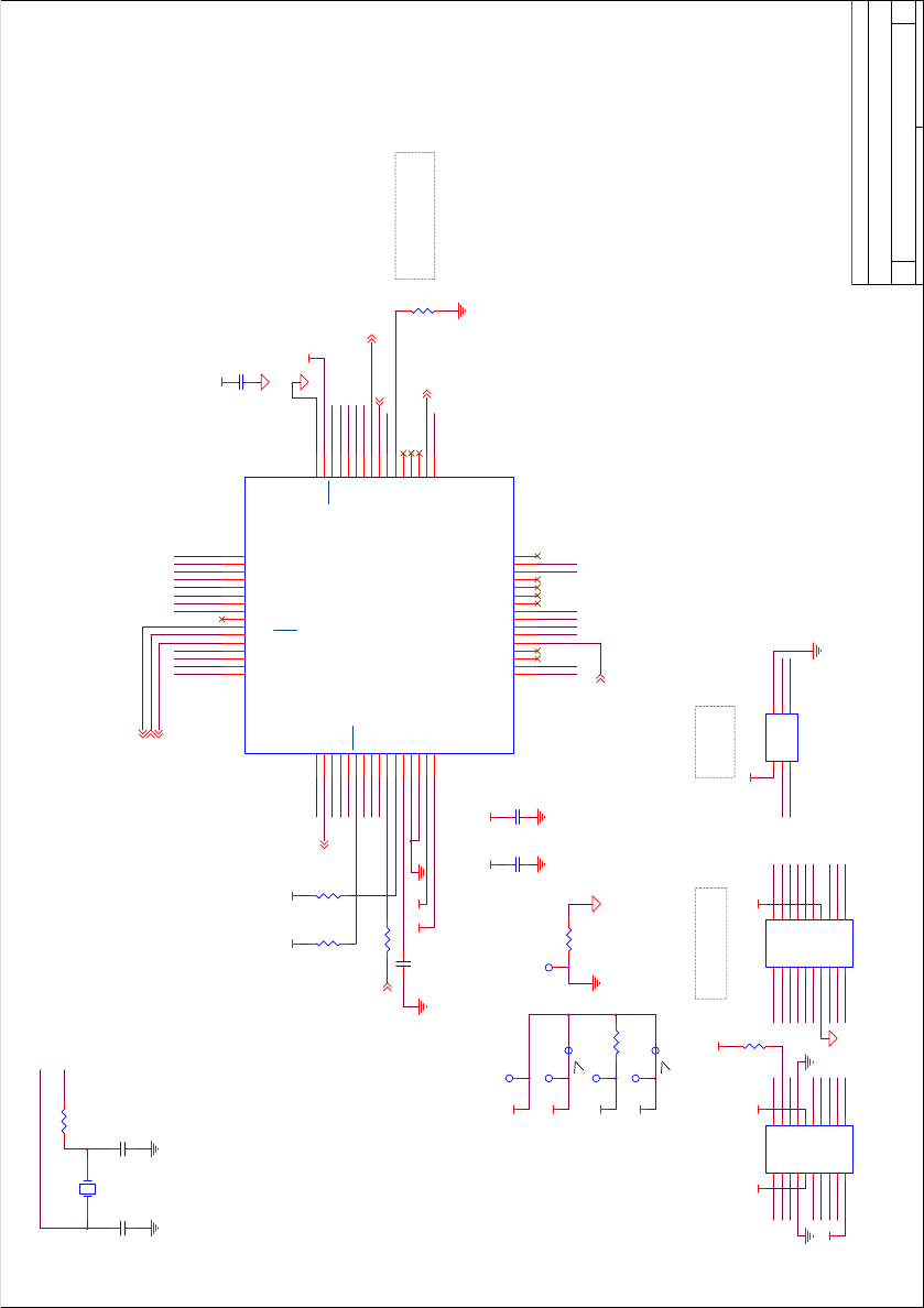
- 17 -
P74
P06 P05
P50
1.27mm Pich Pin Header
T3
1
CN1
20021111-00020T4LF
1 2
3 4
5 6
7 8
910
11
13
15
17
19
12
14
16
18
20
T2
1
U1
uPD78F1146AGA-HAB-AX
P120/INTP0/EXLVI
1
P43
2
P42/TI04/TO04
3
P41/TOOL1
4
P40/TOOL0
5
RESET
6
P124/XT2
7
P123/XT1
8
FLMD0
9
P122/X2/EXC LK
10
P121/X1
11
REGC
12
VSS
13
EVSS
14
VDD
15
EVDD
16
P60/SCL0
17
P61/SDA0
18
P62
19
P63
20
P31/TI03/ TO03/I NTP4
21
P77/KR7/I NTP11
22
P76/KR6/I NTP10
23
P75/KR5/I NTP9
24
P74/KR4/I NTP8
25
P73/KR3
26
P72/KR2
27
P71/KR1
28
P70/KR0
29
P06/TI06/ TO06
30
P05/TI05/ TO05
31
P30/INT P3/RTC1HZ
32
P50/INTP1 33
P51/INTP2 34
P52 35
P53 36
P54 37
P55 38
P17/TI02/TO02 39
P16/TI01/TO01/IN TP5 40
P15/RTCDIV/RTCCL 41
P14/RXD3 42
P13/TXD3 43
P12/SO00/TXD0 44
P11/SI00/RXD0 45
P10/SCK00 46
AVREF 47
AVSS 48
P27/ANI7 49
P26/ANI6 50
P25/ANI5 51
P24/ANI4 52
P23/ANI3 53
P22/ANI2 54
P21/ANI1 55
P20/ANI0 56
P130 57
P04/SCK10/SCL10 58
P03/SI10/R XD1/SD A10 59
P02/SO10/TXD1 60
P01/TO00 61
P00/TI00 62
P141/PCLBUZ1/INTP7 63
P140/PCLBUZ0/INTP6 64
Tit l e
Size Docum ent Number Rev
Date: Sheet of
TS-TCS00874-2 1.0
MB-RF1146
A3
12Friday , March 18, 2011
78K0R/KE3
CLK_OUT2
T5
1
R3
10K
RF1SS
VDD
RF
RF
AVREF
T4
1
SEN2
XT2
XT1
FLMD0
P41
RESET
VDD
SI2
C4 0.47uF/6. 3VB
P40
SO2
C6
0.1uF
VDD
SCLK2
INT2
R2
10K
VDD
WAKE 2
AVREF
RESETn 2
P10
P11
P12
P141
P141
P10
P12
P11
CN2
20021111-00020T4LF
1 2
3 4
5 6
7 8
910
11
13
15
17
19
12
14
16
18
20
P14
AVSS
P24
P26
P10
P12
P17
P140
P00
P20
P22 P23
P25
P27
P11
P13
AVREF
P141
P01
P21
C1
18pF
C2
18pF
Y1
FC-135(32.768KHz)
R1
100
XT2
XT1
AVSS
AVSS
R60
EVDD1SS
R70
T1
1
VDD
P120
P42
P60
P61
J1
SM06B-SRSS-TB(LF )(SN)
1 2
3 4
5 6
P74
R40
(Shield)
C3
0.1uF
AVREF
EVDD
EVDD
C5
0.1uF
P75
P76
P06
P77
R5
1.5K
1 2
P05
UZ,UD判別ポート
プルアップを有効にして、
LowならばUDシリーズ
P50
P17
EVDD
P13
P14
P20
XTAL_32_P 2
P21
P22
P23
P24
P25
P26
P00
P27
P01
P140
AVSS
P120 P42
VDD EVDD
P41 P40
RESET FLMD0
EVDD
P60 P61
P77
1mmPich SMT
Connector
P76
R18
10K
EVDD
P75
5. Circuit diagram
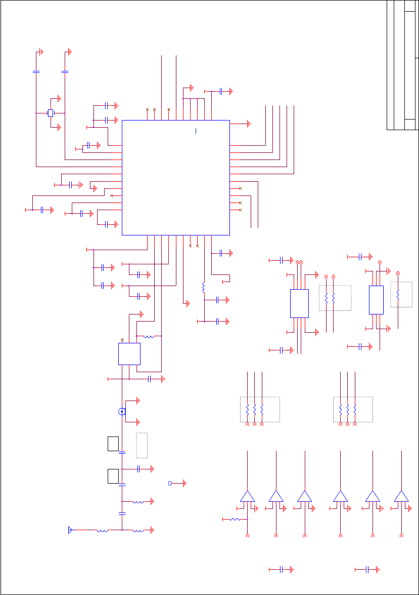
- 18 -
UZ_CLK_OUT
RF
C32
0.1uF
UZ _R ESETn
UZ_WAKE
VDD
C33
0.1uF
UZ_SEN
UZ_SI
UZ_SCLK
UZ_SO
UZ_INT
UZ_XTAL_32_P
Not mount
Not mount
Not mount
Not mount
Not mount
R8
100K
EVDD
H=A->B
L=B->A
U4
SN74LVC2T45DCU
VCCA 1
A1 2
A2 3
B2
6
DIR
5
VCC B
8
GND 4
B1
7
Tit le
Size Document Number Rev
Date: Sheet of
TS-TCS00874-2 1.0
MB- R F 11 46
A3
22Friday , March 18, 2011
H=A->B
L=B->A
U6
SN74LVC1T45DRL
VCCA 1
GND 2
A3
B
4DIR
5VCCB
6
C27
10uF/10V
L4
4.7nH
C28
0.01uF
C26
4.7uF/ 10V
C23
47pF
C7 10pF
C12
47pF
C17
0.01uF
C22
0.1uF
C8
0.01uF
L5
8.2uH
C9 10pF
C10
47pF
C15
39pF
C13
0.01uF
RF
C30
0.1uF
EVDD
UZ2400 (V4.1)
U2
UZ2400V4.1
VDD_RF1
1
GPIO2
11 LOOP_C 40
RF_P
2
RF_N
3
VDD_RF2
4
VDD _GR
5
GND _GR
6
GPIO0
7
GPIO1
8
VDD _2V2
9
VDD _3V
10
GPIO3
12
RESETn
13
C_Comp
14
WAKE
15
INT
16
SO
17
SI
18
SCLK
19
SEN
20
VDD_VCO 39
NC 38
VDD _CP 37
GND _PLL 36
VDD _PLL 35
XTAL_P 34
XTAL_N 33
VDD _A 32
VDD _BG 31
VDD _D 21
XTAL32_P 27
GND _D 22
XTA L 3 2 _ N 28
CLK_OUT 26
SCAN_M 25
RX_QP 30
RF_IP 29
SPI/I2C 23
SCAN _EN 24
PAD
41
C31
0.1uF
C24
10pF
C11
1uF
Y2
NX3225SA-32.000M-STD-CSR-3
1 3
4 2
EVDDRF
C14
47pF
C16
47pF
F1 LDB212G4020C-001
UNB
1
GND
2
BAL 4
GND 5
NC 6
BAL
3
C25
1uF
VDD_RF
VDD_RF
VDD_RF
VDD_RF RF
VDD_RF
RF VDD_RF
VDD_RF
RF
VDD_RF
VDD_RF
R9 xxx
WAKE1
RESETn1
UZ_WAKE
UZ_RESETn
XTAL_32_P1UZ _XTAL_32_P
R10 xxx
R11 xxx
R14 xxx
R15 xxx
R16 xxx
UZ_SEN
UZ_SCLK
UZ_SI
SEN1
SCLK1
SI1
U3A
HD74LV2G34AUSE
1 7
8
4
U3B
HD74LV2G34AUSE
3 5
8
4
U3C
HD74LV2G34AUSE
6 2
8
4
C21
xxxF
C20
0
ANT1
Antenna
1
UZ_SO
L2
1.0nH
L1
1.0nH
SO 1
TP1
PAD
1
INT 1
CN3
MS-156C
CA
FG1 FG2
0Ω
L3
4.7nH
C18
2.7pF
C19
0
0Ω
UZ_INT
UZ_SO
INT 1
SO 1
R12 xxx
R13 xxx
CLK_OUT 1
UZ _C LK_OUT R17 xxx
RF
RF
RF
RESETn1
WAKE1
XTAL_32_P1
UZ_WAKE
UZ _R ESETn
UZ_XTAL_32_P
U5C
HD74LV2G34AUSE
6 2
8
4
U5B
HD74LV2G34AUSE
3 5
8
4
U5A
HD74LV2G34AUSE
1 7
8
4
RF
RF
RF
UZ_SCLK
UZ_SI
UZ_SEN
SI1
SEN1
SCLK1
CLK_OUT 1
RF
C29
0.1uF
RF
C34
0.1uF
UZ_INT
UZ_CLK_OUT
RF VDD
C2012
C1608
32/16/8/4/2/1 MHz Clock output