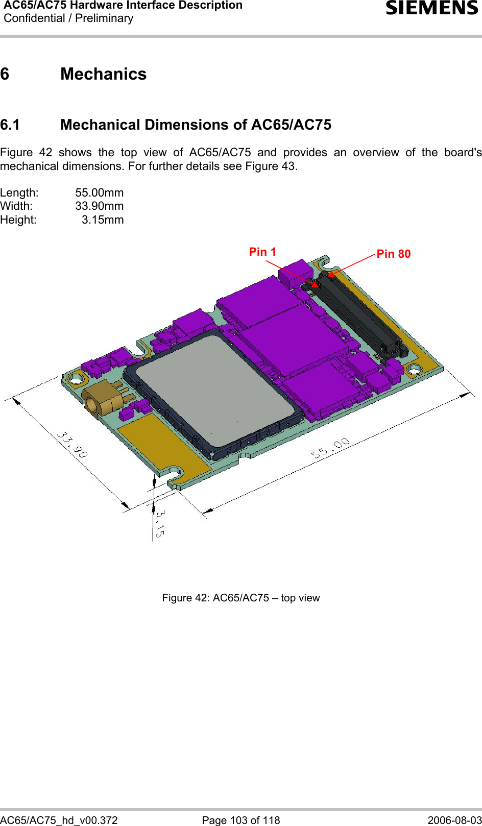
THALES DIS AlS Deutschland AC75 Quad Band GSM Module User Manual AC65 AC75
Gemalto M2M GmbH Quad Band GSM Module AC65 AC75
UserManual.wiki
>
THALES DIS AlS Deutschland
>
AC75 User Manual
User Manual
Navigation menu
Upload a User Manual
Namespaces
Wiki Guide
HTML
PDF
Info
Views
User Manual
Discussion / Help
Navigation
![AC65/AC75 Hardware Interface Description Confidential / Preliminary s AC65/AC75_hd_v00.372 Page 7 of 118 2006-08-03 0 Document History Preceding document: "AC75 Hardware Interface Description" Version 00.251 New document: "AC65/AC75 Hardware Interface Description" Version 00.372 Chapter What is new Throughout document Added new product: AC65 module 1 Added AC65 and general statement on difference between AC65 and AC75. 1.3 Updated list of standards. 1.3.1 Every portable mobile shall have an FCC Grant and IC Certificate of its own. 1.4 Added note on audio safety precautions. 3.5, 9 Removed all information related to specific types of batteries and specific vendors. 3.9 Removed note on required restart of module after removing and reinserting a SIM card during operation. 3.12 Removed section describing USB modem installation. For installation details see [11]. 3.15.4.1 Corrected description of master PCM timing with long or short frame selected. 3.15.4.2 Updated timing for slave mode of PCM interface (Figure 32 and Figure 33). 5.1 Added remark on SELV compliance. 5.5 Table 26: Modified RTC input voltage values (RTC Backup VDDLP). 5.6 Table 27: Different current consumption depending on whether autobauding enabled / disabled. 8.2 Added FCC and IC identifiers for AC65. Changed notes on mobile and fixed devices, added note on portable mobiles. 9.1 Added AC65 incl. Siemens ordering numbers. Preceding document: "AC75 Hardware Interface Description" Version 00.202 New document: "AC75 Hardware Interface Description" Version 00.251 Chapter What is new 3.3.4.2 Corrected description of deferred shutdown. 3.3.4.4 to 3.3.4.6 Alert URCs for undervoltage and overvoltage do not need to enabled by the user. 3.5.3 Added overdischarge release voltage 2.6V 9.1 Specified Siemens ordering numbers for AC75. Preceding document: "AC75 Hardware Interface Description" Version 00.020 New document: "AC75 Hardware Interface Description" Version 00.202 Chapter What is new 3.3.2 New chapter: Signal States after Startup. 3.3.1.1 More detailed description of IGT timing depending on Power-down or Charge-only mode. Added further details on timing after power-up. Added alert message “SHUTDOWN after Illegal PowerUp”](https://usermanual.wiki/THALES-DIS-AlS-Deutschland/AC75/User-Guide-690611-Page-7.png)
![AC65/AC75 Hardware Interface Description Confidential / Preliminary s AC65/AC75_hd_v00.372 Page 9 of 118 2006-08-03 1 Introduction This document applies to the following Siemens products: • AC65 Module • AC75 Module The document describes the hardware of the AC65 and the AC75, both designed to connect to a cellular device application and the air interface. It helps you quickly retrieve interface specifications, electrical and mechanical details and information on the requirements to be considered for integrating further components. The difference between both modules is that AC75 additionally features EGPRS. Please note that except for EGPRS specific statements, all information provided below applies to both module types. Throughout the document, both modules are generally referred to as AC65/AC75. 1.1 Related Documents [1] AC65 AT Command Set 00.372 AC75 AT Command Set 00.372 [2] AC65/AC75 Release Notes 00.372 [3] DSB75 Support Box - Evaluation Kit for Siemens Cellular Engines [4] Application Note 02: Audio Interface Design for GSM Applications (AC65, AC75) [5] Application Note 07: Rechargeable Lithium Batteries in GSM Applications [6] Application Note 16: Upgrading Firmware on MC75, TC6x, AC65, AC75 [7] Application Note 17: Over-The-Air Firmware Update for TC65, AC65, AC75 [8] Application Note 22: Using TTY / CTM Equipment [9] Application Note 26: Power Supply Design for GSM Applications [10] Application Note 24: Application Developer’s Guide [11] Application Note 32: Integrating USB into MC75, TC6x, AC65, AC75 Applications [12] Multiplexer User's Guide [13] Multiplex Driver Developer’s Guide for Windows 2000 and Windows XP [14] Multiplex Driver Installation Guide for Windows 2000 and Windows XP [15] Remote SAT User’s Guide for MC75, TC6x, AC65, AC75 [16] Java User’s Guide for TC65, AC65, AC75 [17] Java doc \wtk\doc\html\index.html](https://usermanual.wiki/THALES-DIS-AlS-Deutschland/AC75/User-Guide-690611-Page-9.png)
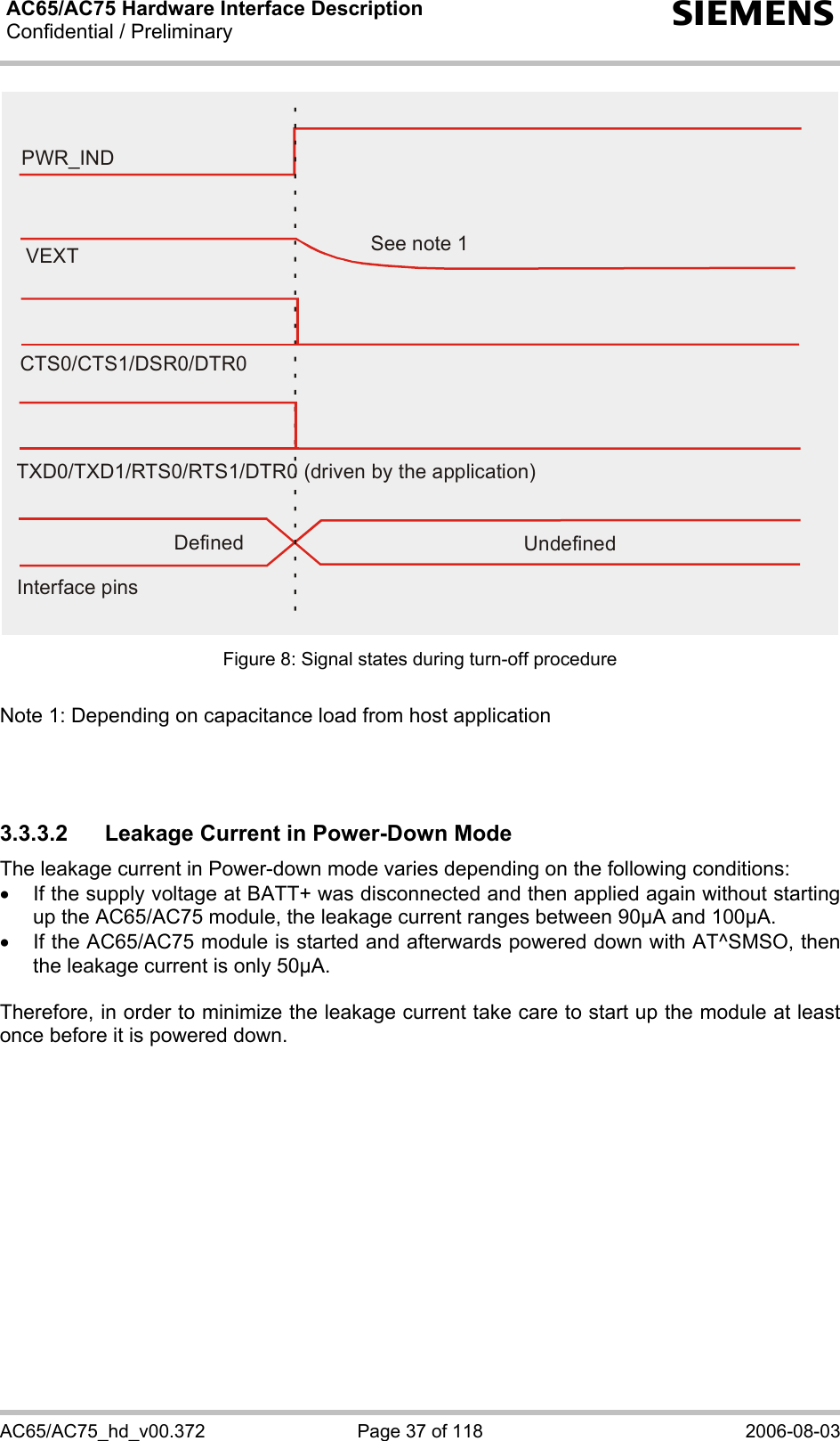
![AC65/AC75 Hardware Interface Description Confidential / Preliminary s AC65/AC75_hd_v00.372 Page 28 of 118 2006-08-03 3.3 Power-Up / Power-Down Scenarios In general, be sure not to turn on AC65/AC75 while it is beyond the safety limits of voltage and temperature stated in Chapter 5.1. AC65/AC75 would immediately switch off after having started and detected these inappropriate conditions. In extreme cases this can cause permanent damage to the module. 3.3.1 Turn on AC65/AC75 AC65/AC75 can be started in a variety of ways as described in the following sections: • Hardware driven start-up by IGT line: starts Normal mode or Airplane mode (see Section 3.3.1.1) • Software controlled reset by AT+CFUN command: starts Normal mode or Airplane mode (see Section 3.3.1.4) • Hardware driven start-up by VCHARGE line: starts charging algorithm and Charge-only mode (see Section 3.3.1.3) • Wake-up from Power-down mode by using RTC interrupt: starts Airplane mode The option whether to start into Normal mode or Airplane mode depends on the settings made with the AT^SCFG command or AT+CALA. With AT+CALA, followed by AT^SMSO the module can be configured to restart into Airplane mode at a scheduled alarm time. Switching back and forth between Normal mode and Airplane mode is possible any time during operation by using the AT^SCFG command. After startup or mode change the following URCs indicate the module’s ready state: • “SYSSTART” indicates that the module has entered Normal mode. • “^SYSSTART AIRPLANE MODE” indicates that the module has entered Airplane mode. • “^SYSSTART CHARGE ONLY MODE” indicates that the module has entered the Charge-only mode. These URCs are indicated only if the module is set to a fixed bit rate, i.e. they do not appear if autobauding is enabled (AT+IPR0). Detailed explanations on AT^SCFG, AT+CFUN, AT+CALA, Airplane mode and AT+IPR can be found in [1]. 3.3.1.1 Turn on AC65/AC75 Using Ignition Line IGT When AC65/AC75 is in Power-down mode or Charge-only mode, it can be started to Normal mode or Airplane mode by driving the IGT (ignition) line to ground. This must be accomplished with an open drain/collector driver to avoid current flowing into this pin. The module will start up when both of the following two conditions are met: • The supply voltage applied at BATT+ must be in the operating range. • The IGT line needs to be driven low for at least 400ms in Power-down mode or at least 2s in Charge-only mode. When released IGT goes high and causes the module to start. Considering different strategies of host application design the figures below show two approaches to meet this requirement: The example in Figure 5 assumes that IGT is activated after BATT+ has already been applied. The example in Figure 6 assumes that IGT is held low before BATT+ is switched on. In either case, to power on the module, ensure that low state of IGT takes at least 400ms (Power-down mode) or 2s (Charge-only mode) from the moment the voltage at BATT+ is available. For Charge-only mode see also Chapter 3.5.6.](https://usermanual.wiki/THALES-DIS-AlS-Deutschland/AC75/User-Guide-690611-Page-28.png)
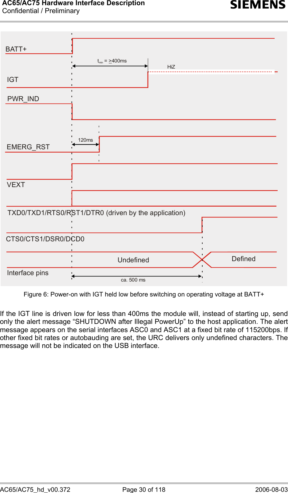
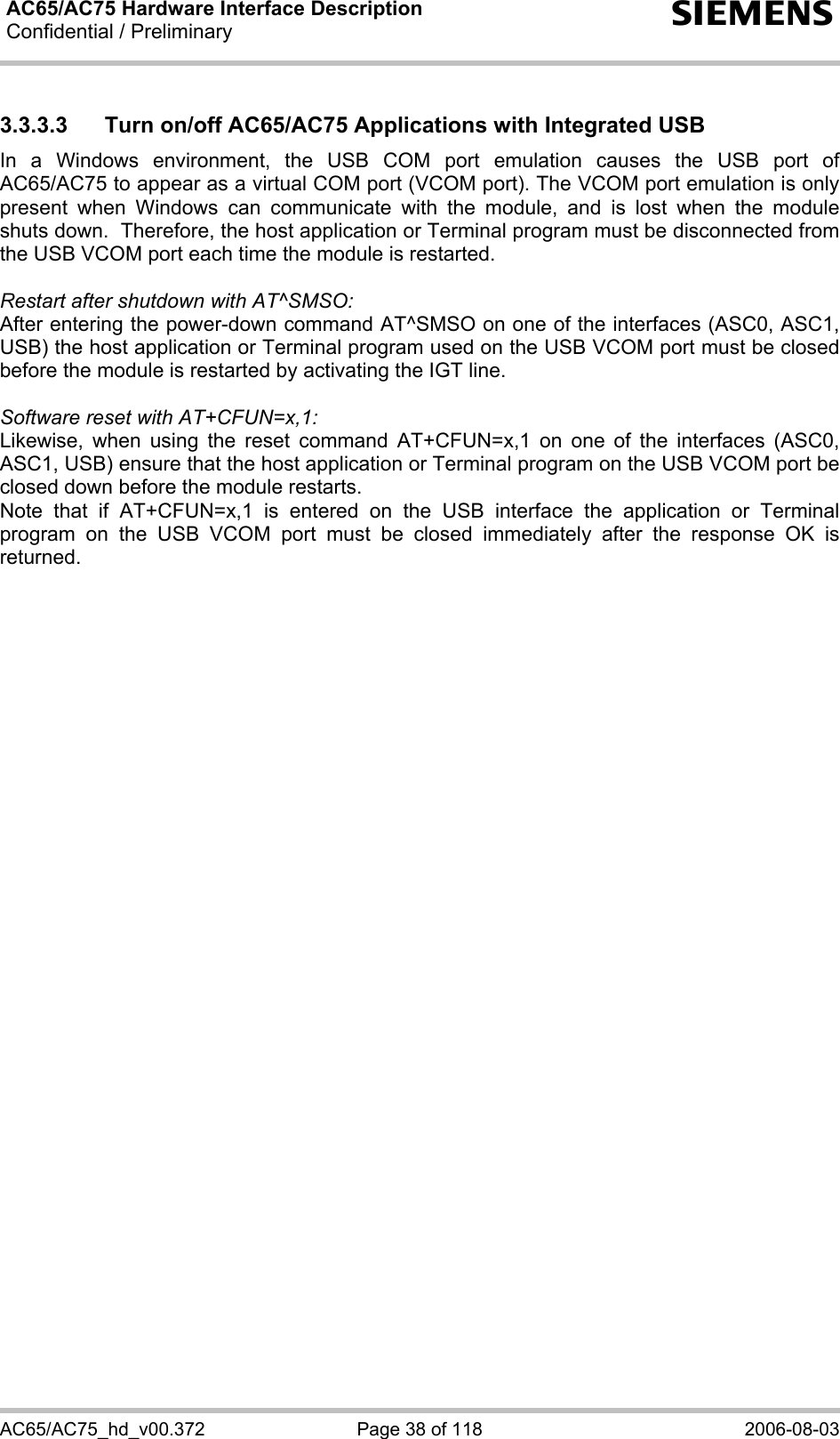
![AC65/AC75 Hardware Interface Description Confidential / Preliminary s AC65/AC75_hd_v00.372 Page 29 of 118 2006-08-03 Assertion of CTS indicates that the module is ready to receive data from the host application. In addition, if configured to a fixed bit rate (AT+IPR0), the module will send the URC “^SYSSTART” or “^SYSSTART AIRPLANE MODE” which notifies the host application that the first AT command can be sent to the module. The duration until this URC is output varies with the SIM card and may take a couple of seconds. Please note that no “^SYSSTART” or “^SYSSTART AIRPLANE MODE” URC will be generated if autobauding (AT+IPR=0) is enabled. To allow the application to detect the ready state of the module we recommend using hardware flow control which can be set with AT\Q or AT+ICF (see [1] for details). The default setting of AC65/AC75 is AT\Q0 (no flow control) which shall be altered to AT\Q3 (RTS/CTS handshake). If the application design does not integrate RTS/CTS lines the host application shall wait at least for the “^SYSSTART” or “^SYSSTART AIRPLANE MODE” URC. However, if the URCs are neither used (due to autobauding) then the only way of checking the module’s ready state is polling. To do so, try to send characters (e.g. “at”) until the module is responding. See also Chapter 3.3.2 “Signal States after Startup” EMERG_RSTVEXTTXD0/TXD1/RTS0/RST1/DTR0 (driven by the application)CTS0/CTS1/DSR0/DCD0ca. 500 msInterface pinsUndefined DefinedPWR_INDt = 400msmin>120msBATT+IGTHiZ Figure 5: Power-on with operating voltage at BATT+ applied before activating IGT](https://usermanual.wiki/THALES-DIS-AlS-Deutschland/AC75/User-Guide-690611-Page-29.png)
![AC65/AC75 Hardware Interface Description Confidential / Preliminary s AC65/AC75_hd_v00.372 Page 32 of 118 2006-08-03 3.3.1.3 Turn on AC65/AC75 Using the VCHARGE Signal As detailed in Section 3.5.6, the charging adapter can be connected regardless of the module’s operating mode. If the charger is connected to the charger input of the external charging circuit and the module’s VCHARGE pin while AC65/AC75 is off, and the battery voltage is above the undervoltage lockout threshold, processor controlled fast charging starts (see Section 3.5.5). AC65/AC75 enters a restricted mode, referred to as Charge-only mode where only the charging algorithm will be launched. During the Charge-only mode AC65/AC75 is neither logged on to the GSM network nor are the serial interfaces fully accessible. To switch from Charge-only mode to Normal mode the ignition line (IGT) must be pulled low for at least 2 seconds. When released, the IGT line goes high and causes the module to enter the Normal mode. See also Section 3.5.6. 3.3.1.4 Reset AC65/AC75 via AT+CFUN Command To reset and restart the AC65/AC75 module use the command AT+CFUN. You can enter AT+CFUN=,1 or AT+CFUN=x,1, where x may be in the range from 0 to 9. See [1] for details. If configured to a fix baud rate (AT+IPR0), the module will send the URC “^SYSSTART” or “^SYSSTART AIRPLANE MODE” to notify that it is ready to operate. If autobauding is enabled (AT+IPR=0) there will be no notification. To register to the network SIM PIN authentication is necessary after restart.](https://usermanual.wiki/THALES-DIS-AlS-Deutschland/AC75/User-Guide-690611-Page-32.png)
![AC65/AC75 Hardware Interface Description Confidential / Preliminary s AC65/AC75_hd_v00.372 Page 39 of 118 2006-08-03 3.3.4 Automatic Shutdown Automatic shutdown takes effect if: • the AC65/AC75 board is exceeding the critical limits of overtemperature or undertemperature • the battery is exceeding the critical limits of overtemperature or undertemperature • undervoltage or overvoltage is detected See Charge-only mode described in Section 3.5.6 for exceptions. The automatic shutdown procedure is equivalent to the Power-down initiated with the AT^SMSO command, i.e. AC65/AC75 logs off from the network and the software enters a secure state avoiding loss of data. Alert messages transmitted before the device switches off are implemented as Unsolicited Result Codes (URCs). The URC presentation mode varies with the condition, please see Chapters 3.3.4.1 to 3.3.4.5 for details. For further instructions on AT commands refer to [1]. 3.3.4.1 Thermal Shutdown The board temperature is constantly monitored by an internal NTC resistor located on the PCB. The NTC that detects the battery temperature must be part of the battery pack circuit as described in 3.5.3 The values detected by either NTC resistor are measured directly on the board or the battery and therefore, are not fully identical with the ambient temperature. Each time the board or battery temperature goes out of range or back to normal, AC65/AC75 instantly displays an alert (if enabled). • URCs indicating the level "1" or "-1" allow the user to take appropriate precautions, such as protecting the module from exposure to extreme conditions. The presentation of the URCs depends on the settings selected with the AT^SCTM write command: AT^SCTM=1: Presentation of URCs is always enabled. AT^SCTM=0 (default): Presentation of URCs is enabled for 15 seconds time after start-up of AC65/AC75. After 15 seconds operation, the presentation will be disabled, i.e. no alert messages can be generated. • URCs indicating the level "2" or "-2" are instantly followed by an orderly shutdown. The presentation of these URCs is always enabled, i.e. they will be output even though the factory setting AT^SCTM=0 was never changed. The maximum temperature ratings are stated in Chapter 5.2. Refer to Table 7 for the associated URCs.](https://usermanual.wiki/THALES-DIS-AlS-Deutschland/AC75/User-Guide-690611-Page-39.png)
![AC65/AC75 Hardware Interface Description Confidential / Preliminary s AC65/AC75_hd_v00.372 Page 40 of 118 2006-08-03 Table 7: Temperature dependent behavior Sending temperature alert (2min after AC65/AC75 start-up, otherwise only if URC presentation enabled) ^SCTM_A: 1 Caution: Battery close to overtemperature limit. ^SCTM_B: 1 Caution: Bboard close to overtemperature limit. ^SCTM_A: -1 Caution: Battery close to undertemperature limit. ^SCTM_B: -1 Caution: Board close to undertemperature limit. ^SCTM_A: 0 Battery back to uncritical temperature range. ^SCTM_B: 0 Board back to uncritical temperature range. Automatic shutdown (URC appears no matter whether or not presentation was enabled) ^SCTM_A: 2 Alert: Battery equal or beyond overtemperature limit. AC65/AC75 switches off. ^SCTM_B: 2 Alert: Board equal or beyond overtemperature limit. AC65/AC75 switches off. ^SCTM_A: -2 Alert: Battery equal or below undertemperature limit. AC65/AC75 switches off. ^SCTM_B: -2 Alert: Board equal or below undertemperature limit. AC65/AC75 switches off. 3.3.4.2 Deferred Shutdown at Extreme Temperature Conditions In the following cases, shutdown will be deferred if a critical temperature limit is exceeded: • while an emergency call is in progress • during a two minute guard period after power-up. This guard period has been introduced in order to allow the user to make an emergency call. The start of an emergency call extends the guard period until the end of the call. Any other network activity may be terminated by shutdown upon expiry of the guard time. The guard period starts again when the module registers to the GSM network the first time after power-up. If the temperature is still out of range after the guard period expires or the call ends, the module switches off immediately (without another alert message). CAUTION! Automatic shutdown is a safety feature intended to prevent damage to the module. Extended usage of the deferred shutdown functionality may result in damage to the module, and possibly other severe consequences. 3.3.4.3 Monitoring the Board Temperature of AC65/AC75 The AT^SCTM command can also be used to check the present status of the board. Depending on the selected mode, the read command returns the current board temperature in degrees Celsius or only a value that indicates whether the board is within the safe or critical temperature range. See [1] for further instructions. 3.3.4.4 Undervoltage Shutdown if Battery NTC is Present In applications where the module’s charging technique is used and an NTC is connected to the BATT_TEMP terminal, the software constantly monitors the applied voltage. If the measured battery voltage is no more sufficient to set up a call the following URC will be presented: ^SBC: Undervoltage.](https://usermanual.wiki/THALES-DIS-AlS-Deutschland/AC75/User-Guide-690611-Page-40.png)
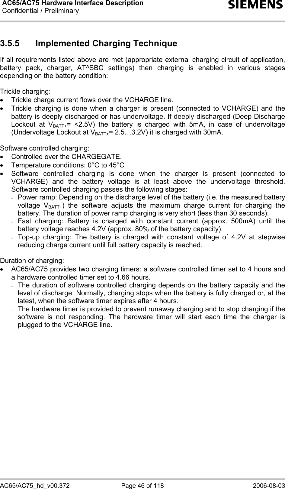
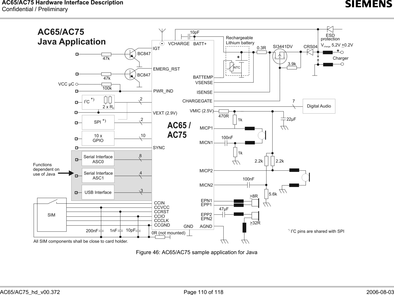
![AC65/AC75 Hardware Interface Description Confidential / Preliminary s AC65/AC75_hd_v00.372 Page 43 of 118 2006-08-03 3.5 Charging Control AC65/AC75 integrates a charging management for rechargeable Lithium Ion and Lithium Polymer batteries. You can skip this chapter if charging is not your concern, or if you are not using the implemented charging algorithm. The following sections contain an overview of charging and battery specifications. Please refer to [4] for greater detail, especially regarding requirements for batteries and chargers, appropriate charging circuits, recommended batteries and an analysis of operational issues typical of battery powered GSM/GPRS applications. 3.5.1 Hardware Requirements AC65/AC75 has no on-board charging circuit. To benefit from the implemented charging management you are required to install a charging circuit within your application according to the Figure 46. 3.5.2 Software Requirements Use the command AT^SBC, parameter <current>, to enter the current consumption of the host application. This information enables the AC65/AC75 module to correctly determine the end of charging and terminate charging automatically when the battery is fully charged. If the <current> value is inaccurate and the application draws a current higher than the final charge current, either charging will not be terminated or the battery fails to reach its maximum voltage. Therefore, the termination condition is defined as: current consumption dependent on the operating mode of the ME plus current consumption of the external application. If used the current flowing over the VEXT pin of the application interface must be added, too. The parameter <current> is volatile, meaning that the factory default (0mA) is restored each time the module is powered down or reset. Therefore, for better control of charging, it is recommended to enter the value every time the module is started. See [1] for details on AT^SBC.](https://usermanual.wiki/THALES-DIS-AlS-Deutschland/AC75/User-Guide-690611-Page-43.png)
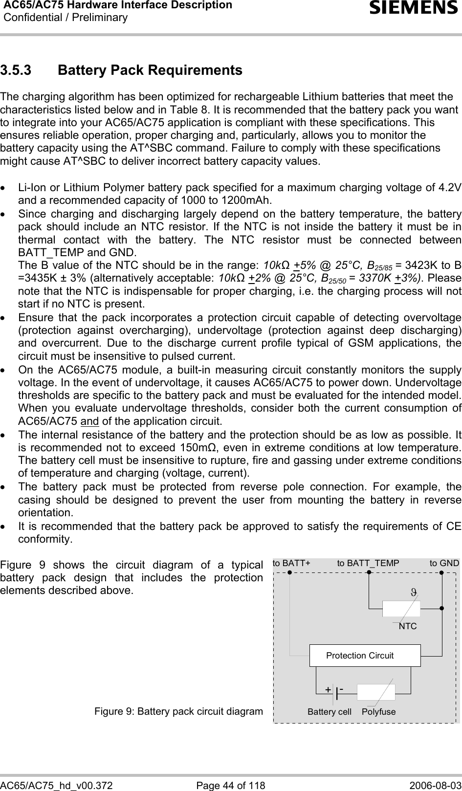
![AC65/AC75 Hardware Interface Description Confidential / Preliminary s AC65/AC75_hd_v00.372 Page 45 of 118 2006-08-03 Table 8: Specifications of battery packs suitable for use with AC65/AC75 Battery type Rechargeable Lithium Ion or Lithium Polymer battery Nominal voltage 3.6V / 3.7V Capacity Recommended: 1000mAh to 1200mAh Minimum: 500mAh NTC 10k ± 5% @ 25°C approx. 5k @ 45°C approx. 26.2k @ 0°C B value range: B (25/85)=3423K to B =3435K ± 3% Overcharge detection voltage 4.325 ± 0.025V Overdischarge detection voltage 2.5V Overdischarge release voltage 2.6V Overcurrent detection 3 ± 0.5A Overcurrent detection delay time 4 ~ 16ms Short detection delay time 50µs Internal resistance <130m Note: A maximum internal resistance of 150m should not be exceeded even after 500 cycles and under extreme conditions. 3.5.4 Charger Requirements For using the implemented charging algorithm and the reference charging circuit recommended in [4] and in Figure 46, the charger has to meet the following requirements: Output voltage: 5.2Volts ±0.2V (stabilized voltage) Output current: 500mA Chargers with a higher output current are acceptable, but please consider that only 500mA will be applied when a 0.3Ohms shunt resistor is connected between VSENSE and ISENSE. See [4] for further details.](https://usermanual.wiki/THALES-DIS-AlS-Deutschland/AC75/User-Guide-690611-Page-45.png)
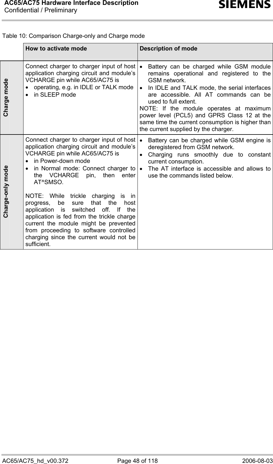
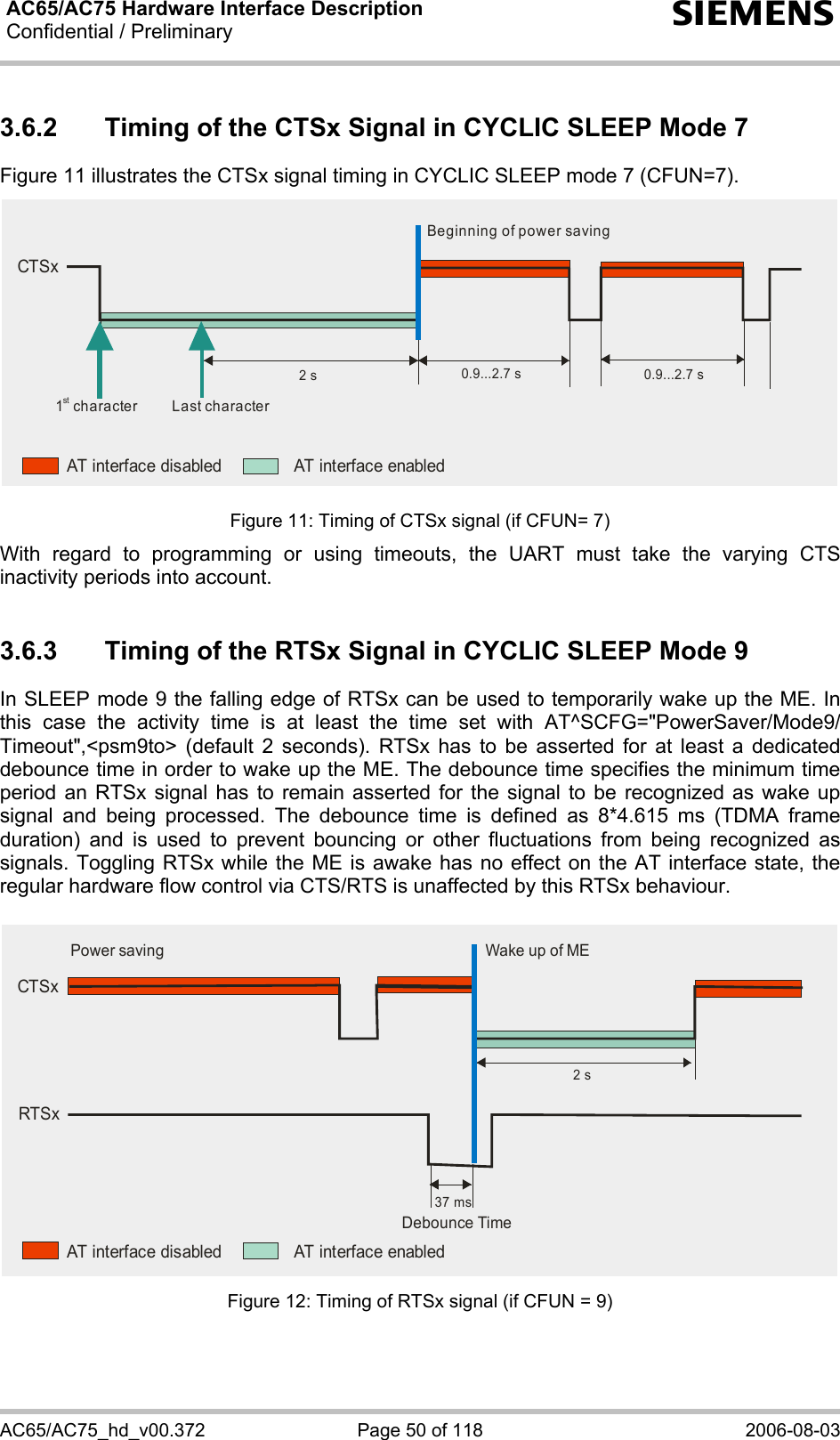
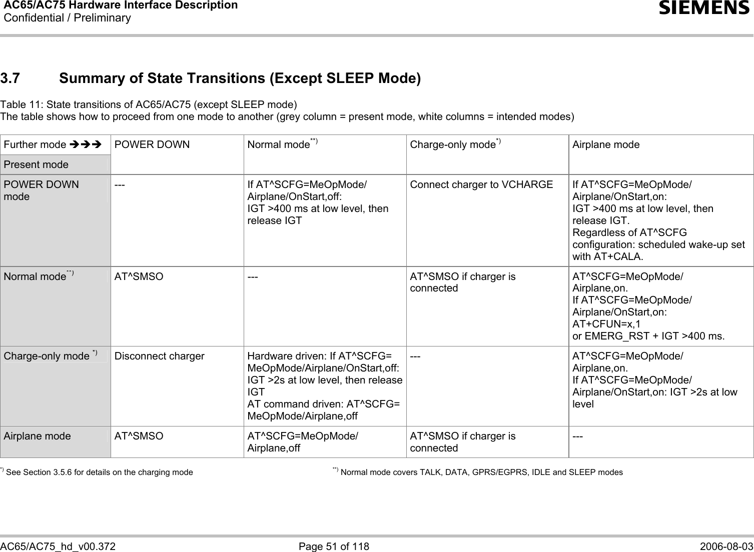
![AC65/AC75 Hardware Interface Description Confidential / Preliminary s AC65/AC75_hd_v00.372 Page 49 of 118 2006-08-03 3.6 Power Saving Intended for power saving, SLEEP mode reduces the functionality of the AC65/AC75 to a minimum and thus minimizes the current consumption. Settings can be made using the AT+CFUN command. For details see [1]. SLEEP mode falls in two categories: • NON-CYCLIC SLEEP mode: AT+CFUN = 0 • CYCLIC SLEEP modes, AT+CFUN = 7 or 9. The functionality level AT+CFUN=1 is where power saving is switched off. This is the default after startup. NON-CYCLIC SLEEP mode permanently blocks the serial interface. The benefit of the CYCLIC SLEEP mode is that the serial interface remains accessible and that, in intermittent wake-up periods, characters can be sent or received without terminating the selected mode. This allows the AC65/AC75 to wake up for the duration of an event and, afterwards, to resume power saving. Please refer to [1] for a summary of all SLEEP modes and the different ways of waking up the module. For CYCLIC SLEEP mode both the AC65/AC75 and the application must be configured to use hardware flow control. This is necessary since the CTSx signal is set/reset every 0.9-2.7 seconds in order to indicate to the application when the UART is active. Please refer to [1] for details on how to configure hardware flow control for the AC65/AC75. Note: Although not explicitly stated, all explanations given in this section refer equally to ASC0 and ASC1, and accordingly to CTS0 and CTS1 or RTS0 and RTS1. 3.6.1 Network Dependency of SLEEP Modes The power saving possibilities of SLEEP modes depend on the network the module is registered in. The paging timing cycle varies with the base station. The duration of a paging interval can be calculated from the following formula: t = 4.615 ms (TDMA frame duration) * 51 (number of frames) * DRX value. DRX (Discontinuous Reception) is a value from 2 to 9, resulting in paging intervals from 0.47-2.12 seconds. The DRX value of the base station is assigned by the network operator. In the pauses between listening to paging messages, the module resumes power saving, as shown in Figure 10. Figure 10: Power saving and paging The varying pauses explain the different potential for power saving. The longer the pause the less power is consumed. 0.47-2.12 s 0.47-2.12 s 0.47-2.12 sPaging Paging Paging PagingPower Saving Power Saving Power Saving](https://usermanual.wiki/THALES-DIS-AlS-Deutschland/AC75/User-Guide-690611-Page-49.png)
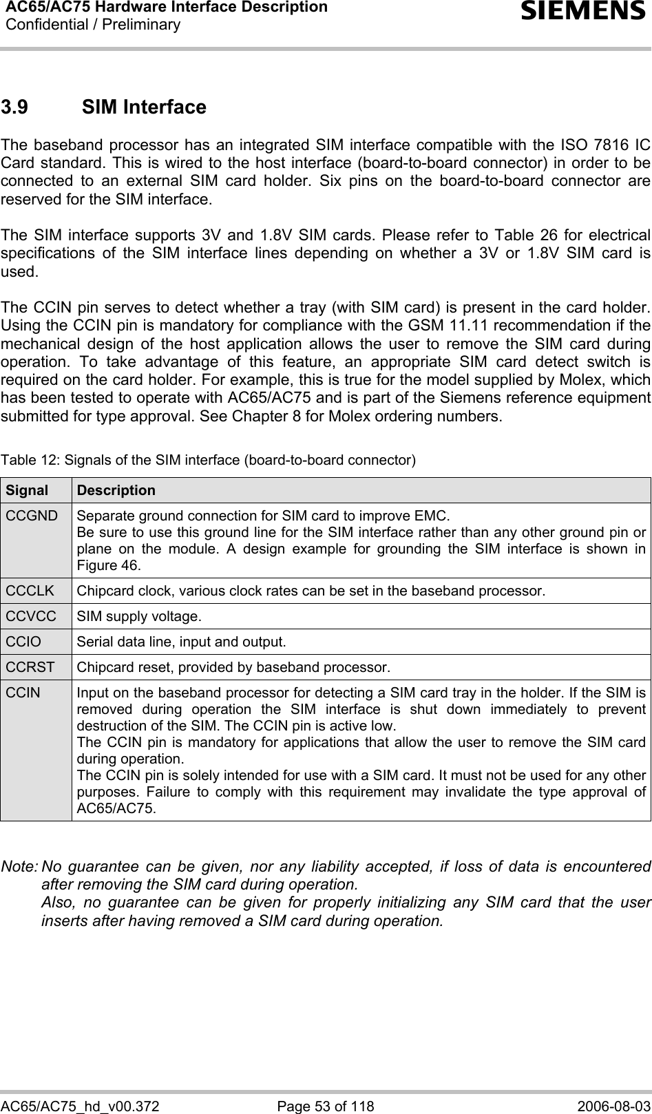
![AC65/AC75 Hardware Interface Description Confidential / Preliminary s AC65/AC75_hd_v00.372 Page 55 of 118 2006-08-03 3.10 Serial Interface ASC0 AC65/AC75 offers an 8-wire unbalanced, asynchronous modem interface ASC0 conforming to ITU-T V.24 protocol DCE signalling. The electrical characteristics do not comply with ITU-T V.28. The significant levels are 0V (for low data bit or active state) and 2.9V (for high data bit or inactive state). For electrical characteristics please refer to Table 26. AC65/AC75 is designed for use as a DCE. Based on the conventions for DCE-DTE connections it communicates with the customer application (DTE) using the following signals: • Port TXD @ application sends data to the module’s TXD0 signal line • Port RXD @ application receives data from the module’s RXD0 signal line Figure 16: Serial interface ASC0 Features • Includes the data lines TXD0 and RXD0, the status lines RTS0 and CTS0 and, in addition, the modem control lines DTR0, DSR0, DCD0 and RING0. • ASC0 is primarily designed for controlling voice calls, transferring CSD, fax and GPRS data and for controlling the GSM engine with AT commands. • Full Multiplex capability allows the interface to be partitioned into three virtual channels, yet with CSD and fax services only available on the first logical channel. Please note that when the ASC0 interface runs in Multiplex mode, ASC1 cannot be used. For more details on Multiplex mode see [10]. • The DTR0 signal will only be polled once per second from the internal firmware of AC65/AC75. • The RING0 signal serves to indicate incoming calls and other types of URCs (Unsolicited Result Code). It can also be used to send pulses to the host application, for example to wake up the application from power saving state. See [1] for details on how to configure the RING0 line by AT^SCFG. • By default, configured for 8 data bits, no parity and 1 stop bit. The setting can be changed using the AT command AT+ICF and, if required, AT^STPB. For details see [1]. • ASC0 can be operated at fixed bit rates from 300 bps to 460,800 bps. • Autobauding supports bit rates from 1,200 to 460,800 bps. • Autobauding is not compatible with multiplex mode. • Supports RTS0/CTS0 hardware flow control and XON/XOFF software flow control. TXD0RXD0RTS0DCD0CTS0DTR0DSR0RING0TXDRXDRTSDCDCTSDTRDSRRINGGSM Module (DCE) Application (DTE)](https://usermanual.wiki/THALES-DIS-AlS-Deutschland/AC75/User-Guide-690611-Page-55.png)
![AC65/AC75 Hardware Interface Description Confidential / Preliminary s AC65/AC75_hd_v00.372 Page 57 of 118 2006-08-03 3.11 Serial Interface ASC1 The ASC1 interface is available as a 4-wire unbalanced, asynchronous modem interface ASC1 conforming to ITU-T V.24 protocol DCE signalling. The electrical characteristics do not comply with ITU-T V.28. The significant levels are 0V (for low data bit or active state) and 2.9V (for high data bit or inactive state). For electrical characteristics please refer to Table 26. AC65/AC75 is designed for use as a DCE. Based on the conventions for DCE-DTE connections it communicates with the customer application (DTE) using the following signals: • Port TXD @ application sends data to module’s TXD1 signal line • Port RXD @ application receives data from the module’s RXD1 signal line Figure 17: Serial interface ASC1 Features • Includes only the data lines TXD1 and RXD1 plus RTS1 and CTS1 for hardware handshake. • On ASC1 no RING line is available. The indication of URCs on the second interface depends on the settings made with the AT^SCFG command. For details refer to [1]. • Configured for 8 data bits, no parity and 1 or 2 stop bits. • ASC1 can be operated at fixed bit rates from 300 bps to 460,800 bps. Autobauding is not supported on ASC1. • Supports RTS1/CTS1 hardware flow control and XON/XOFF software flow control. Table 14: DCE-DTE wiring of ASC1 DCE DTE V.24 circuit Pin function Signal direction Pin function Signal direction 103 TXD1 Input TXD Output 104 RXD1 Output RXD Input 105 RTS1 Input RTS Output 106 CTS1 Output CTS Input TXD1RXD1RTS1CTS1TXDRXDRTSCTSGSM Module (DCE) Application (DTE)](https://usermanual.wiki/THALES-DIS-AlS-Deutschland/AC75/User-Guide-690611-Page-57.png)
![AC65/AC75 Hardware Interface Description Confidential / Preliminary s AC65/AC75_hd_v00.372 Page 58 of 118 2006-08-03 3.12 USB Interface AC65/AC75 supports a USB 2.0 Full Speed (12Mbit/s) device interface. It can be operated on a USB 2.0 Full Speed or High Speed root hub (a PC host), but not on a generic USB 2.0 High Speed hub which translates High Speed (480 Mbit/s/) to Full Speed (12 Mbit/s). The USB port has different functions depending on whether or not Java is running. Under Java, the lines may be used for debugging purposes (see [16] for further detail). If Java is not used, the USB interface is available as a command and data interface and for downloading firmware. The USB I/O-pins are capable of driving the signal at min 3.0V. They are 5V I/O compliant. The USB host is responsible for supplying, across the VUSB_IN line, power to the module’s USB interface, but not to other AC65/AC75 interfaces. This is because AC65/AC75 is designed as a self-powered device compliant with the “Universal Serial Bus Specification Revision 2.0”2. MCU USBTransceiverlin.RegulatorPSUBaseband controller GSM moduleHost22Ohms22Ohms1.5kOhmsUSB_DPUSB_DNVUSB_IN5V3.2VD+D-VBUSGND80 pole board-to-board connector Figure 18: USB circuit To properly connect the module’s USB interface to the host a USB 2.0 compatible connector is required. For more information on how to install a USB modem driver and on how to integrate USB into AC65/AC75 applications see [11]. 2 The specification is ready for download on http://www.usb.org/developers/docs/](https://usermanual.wiki/THALES-DIS-AlS-Deutschland/AC75/User-Guide-690611-Page-58.png)
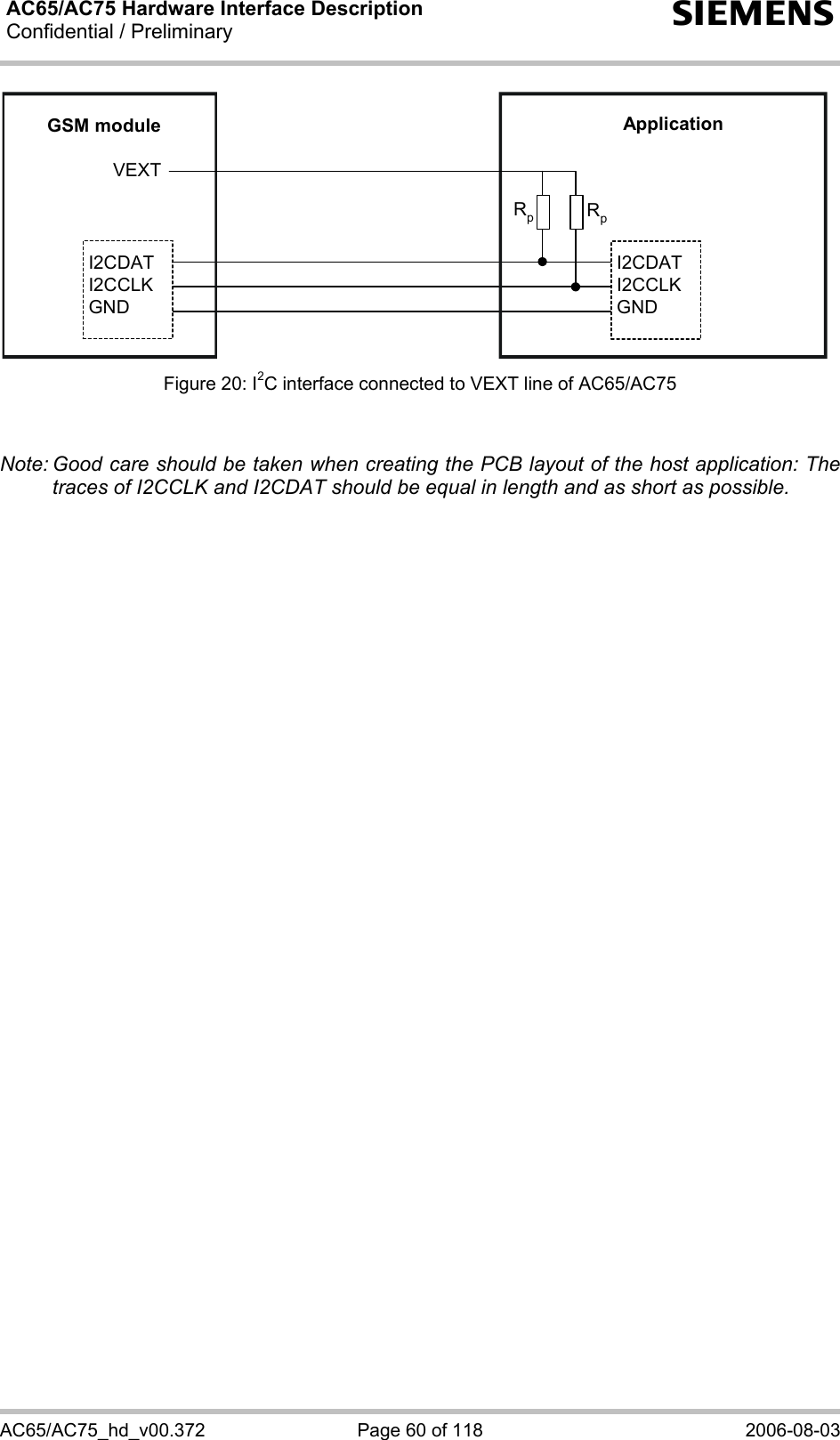
![AC65/AC75 Hardware Interface Description Confidential / Preliminary s AC65/AC75_hd_v00.372 Page 59 of 118 2006-08-03 3.13 I2C Interface I2C is a serial, 8-bit oriented data transfer bus for bit rates up to 400kbps in Fast mode. It consists of two lines, the serial data line I2CDAT and the serial clock line I2CCLK. The AC65/AC75 module acts as a single master device, e.g. the clock I2CCLK is driven by module. I2CDAT is a bi-directional line. Each device connected to the bus is software addressable by a unique 7-bit address, and simple master/slave relationships exist at all times. The module operates as master-transmitter or as master-receiver. The customer application transmits or receives data only on request of the module. To configure and activate the I2C bus use the AT^SSPI command. If the I2C bus is active the two lines I2CCLK and I2DAT are locked for use as SPI lines. Vice versa, the activation of the SPI locks both lines for I2C. Detailed information on the AT^SSPI command as well explanations on the protocol and syntax required for data transmission can be found in [1]. The I2C interface can be powered from an external supply or via the VEXT line of AC65/AC75. If connected to the VEXT line the I2C interface will be properly shut down when the module enters the Power-down mode. If you prefer to connect the I2C interface to an external power supply, take care that VCC of the application is in the range of VVEXT and that the interface is shut down when the PWR_IND signal goes high. See figures below as well as Section 7 and Figure 46. In the application I2CDAT and I2CCLK lines need to be connected to a positive supply voltage via a pull-up resistor. For electrical characteristics please refer to Table 26. GSM moduleI2CDATI2CCLKGNDI2CDATI2CCLKGNDApplicationVCCRpRpwVEXT Figure 19: I2C interface connected to VCC of application](https://usermanual.wiki/THALES-DIS-AlS-Deutschland/AC75/User-Guide-690611-Page-59.png)
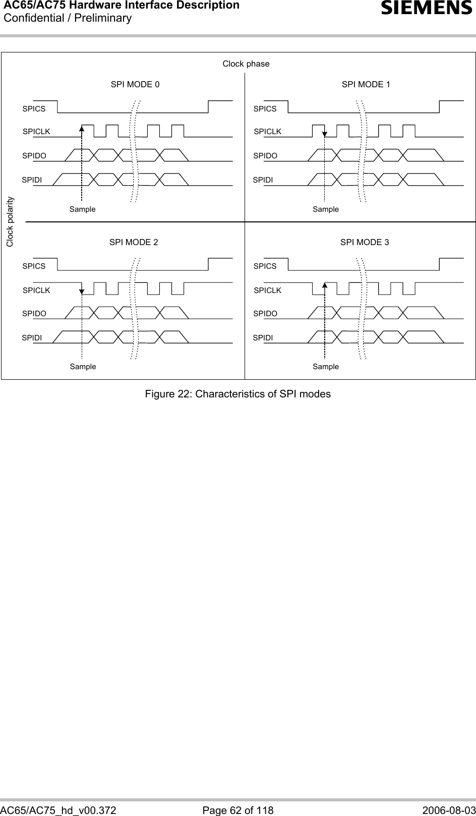
![AC65/AC75 Hardware Interface Description Confidential / Preliminary s AC65/AC75_hd_v00.372 Page 61 of 118 2006-08-03 3.14 SPI Interface The SPI (serial peripheral interface) is a synchronous serial interface for control and data transfer between the AC65/AC75 module and the connected application. Only one application can be connected to the module’s SPI. The interface supports transmission rates up to 6.5Mbit/s. It consists of four lines, the two data lines SPIDI/SPIDO, the clock line SPICLK and the chip select line SPICS. The AC65/AC75 module acts as a single master device, e.g. the clock SPICLK is driven by module. Whenever the SPICS pin is in a low state, the SPI bus is activated and data can be transferred from the module and vice versa. The SPI interface uses two independent lines for data input (SPIDI) and data output (SPIDO). GSM module ApplicationSPICLK SPICLKSPICS SPICSSPIDOSPIDI SPIDISPIDO Figure 21: SPI interface To configure and activate the SPI bus use the AT^SSPI command. If the SPI bus is active the two lines I2CCLK and I2DAT are locked for use as I2C lines. Detailed information on the AT^SSPI command as well explanations on the SPI modes required for data transmission can be found in [1]. In general, SPI supports four operation modes. The modes are different in clock phase and clock polarity. The module’s SPI mode can be configured by using the AT command AT^SSPI. Make sure the module and the connected slave device works with the same SPI mode. Figure 22 shows the characteristics of the four SPI modes. The SPI modes 0 and 3 are the most common used modes. For electrical characteristics please refer to Table 26.](https://usermanual.wiki/THALES-DIS-AlS-Deutschland/AC75/User-Guide-690611-Page-61.png)
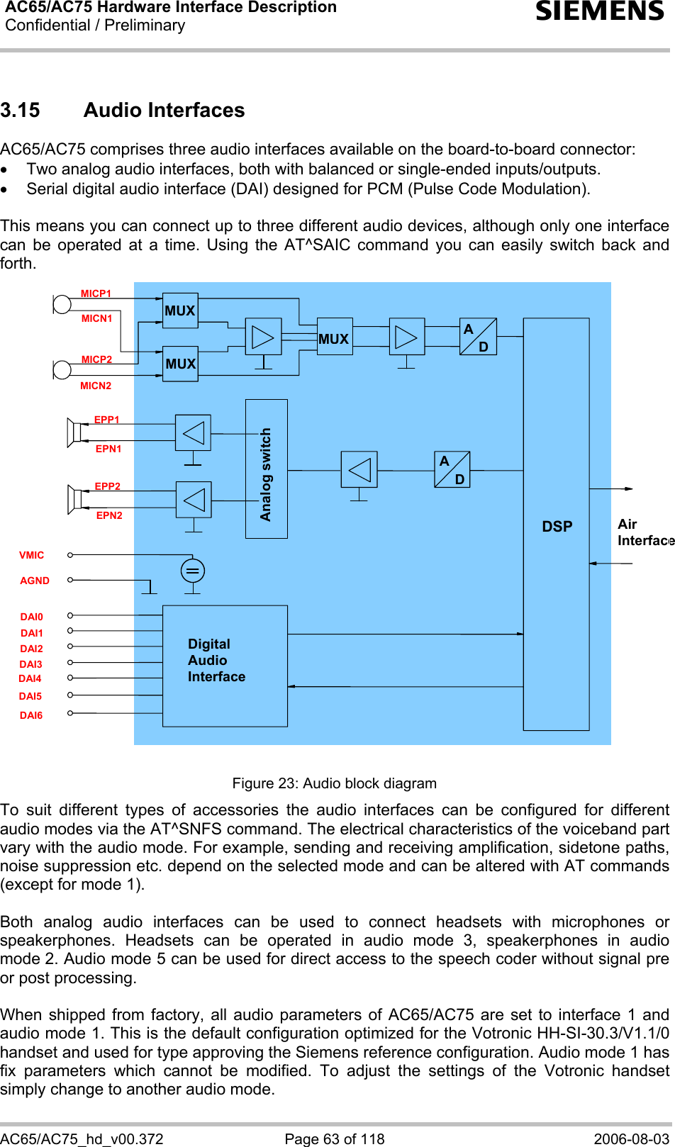
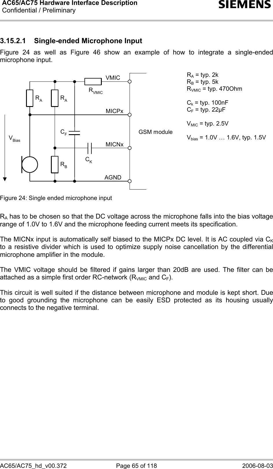
![AC65/AC75 Hardware Interface Description Confidential / Preliminary s AC65/AC75_hd_v00.372 Page 66 of 118 2006-08-03 3.15.2.2 Differential Microphone Input Figure 25 shows a differential solution for connecting an electret microphone. GSM moduleRARAVBias CKAGNDMICNxMICPxVMICCFRVMIC RA = typ. 1k RVMIC = 470Ohm CK = typ. 100nF CF = typ. 22µF VMIC = typ. 2.5V Vbias = 1.0V … 1.6V, typ. 1.5V Figure 25: Differential microphone input The advantage of this circuit is that it can be used if the application involves longer lines between microphone and module. While VMIC is switched off, the input voltage at any MIC pin should not exceed ±0.25V relative to AGND (see also Chapter 5.1). In this case no bias voltage has to be supplied from the customer circuit to the MIC pin and any signal voltage should be smaller than Vpp = 0.5V. VMIC can be used to generate the MICP-pin bias voltage as shown below. In this case the bias voltage is only applied if VMIC is switched on. Only if VMIC is switched on, can the voltage applied to any MIC pin be in the range of 2.4V to 0V. If these limits are exceeded undervoltage shutdown may be caused. Consider that the maximum full scale input voltage is Vpp = 1.6V. The behavior of VMIC can be controlled with the parameter micVccCtl of the AT command AT^SNFM (see [1]): • micVccCtl=2 (default). VMIC is controlled automatically by the module. VMIC is always switched on while the internal audio circuits of the module are active (e.g., during a call). VMIC can be used as indicator for active audio in the module. • micVccCtl=1. VMIC is switched on continuously. This setting can be used to supply the microphone in order to use the signal in other customer circuits as well. However, this setting leads to a higher current consumption in SLEEP modes. • micVccCtl=0. VMIC is permanently switched off.](https://usermanual.wiki/THALES-DIS-AlS-Deutschland/AC75/User-Guide-690611-Page-66.png)
![AC65/AC75 Hardware Interface Description Confidential / Preliminary s AC65/AC75_hd_v00.372 Page 69 of 118 2006-08-03 3.15.4 Digital Audio Interface (DAI) The DAI can be used to connect audio devices capable of PCM (Pulse Code Modulation) or for type approval. The following chapters describe the PCM interface functionality. The PCM functionality allows the use of a codec like for example the MC145483. This codec replaces the analog audio inputs and outputs during a call, if digital audio is selected by AT^SAIC. The PCM interface is configurable with the AT^SAIC command (see [1]) and supports the following features: - Master and slave mode - Short frame and long frame synchronization - 256 kHz or 512 kHz bit clock frequency For the PCM interface configuration the parameters <clock>, <mode> and <framemode> of the AT^SAIC command are used. The following table lists possible combinations: Table 15: Configuration combinations for the PCM interface Configuration <clock> <mode> <framemode> Master, 256kHz, short frame 0 0 0 Master, 256kHz, long frame 0 0 1 Master, 512kHz, short frame 1 0 0 Master, 512kHz, long frame 1 0 1 Slave, 256kHz, short frame 0 or 13 1 0 Slave, 256kHz, long frame 0 or 1 1 1 Slave, 512kHz, short frame 0 or 1 1 0 Slave, 512kHz, long frame 0 or 1 1 1 In all configurations the PCM interface has the following common features: - 16 Bit linear - 8 kHz sample rate - the most significant bit MSB is transferred first - 125 µs frame duration - common frame sync signal for transmit and receive 3 In slave mode the BCLKIN signal is directly used for data shifting. Therefore, the clock frequency setting is not evaluated and may be either 0 or 1.](https://usermanual.wiki/THALES-DIS-AlS-Deutschland/AC75/User-Guide-690611-Page-69.png)
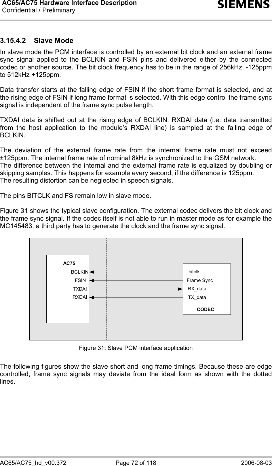
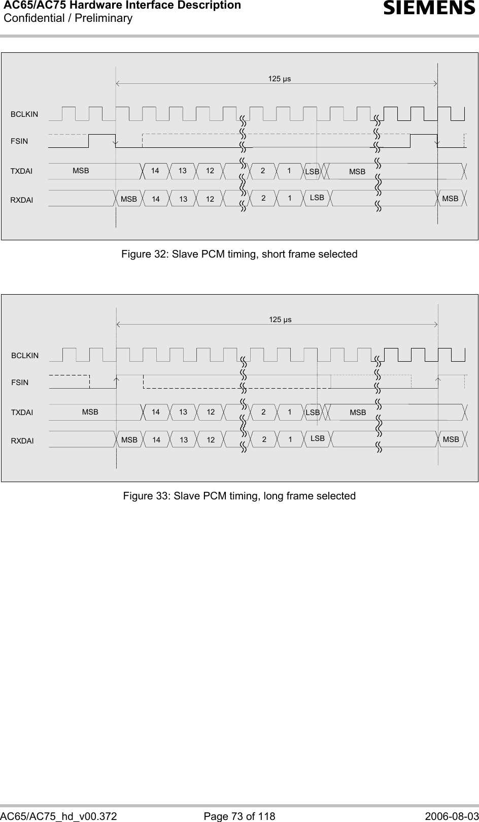
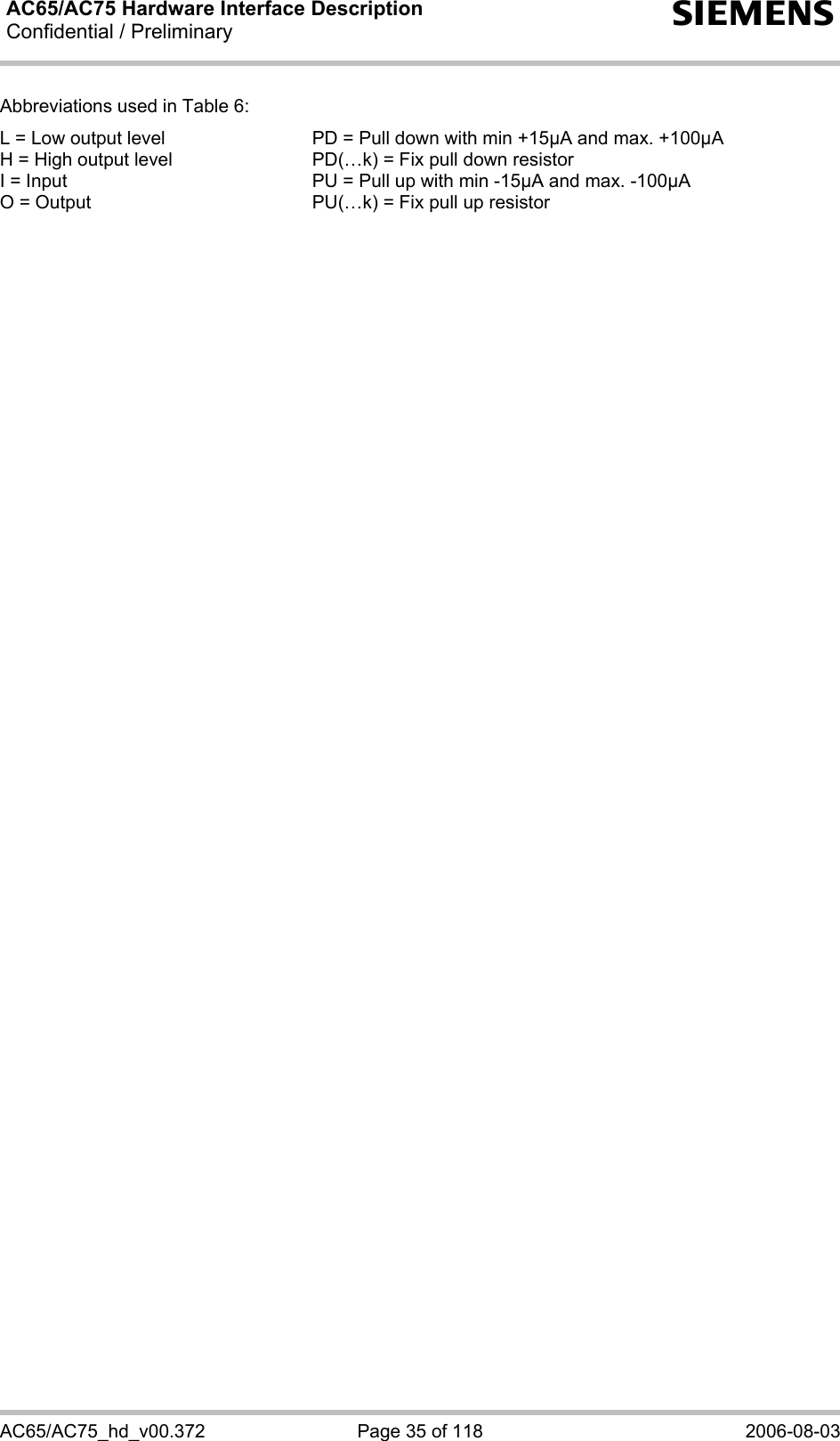
![AC65/AC75 Hardware Interface Description Confidential / Preliminary s AC65/AC75_hd_v00.372 Page 74 of 118 2006-08-03 3.16 GPIO Interface The AC65/AC75 has 10 GPIOs for external hardware devices. Each GPIO can be configured for use as input or output. All settings are AT command controlled. The GIPO related AT commands are the following: AT^SPIO, AT^SCPIN, AT^SCPOL, AT^SCPORT, AT^SDPORT, AT^SGIO, AT^SSIO. A detailed description can be found in [1]. 3.16.1 Using the GPIO10 Pin as Pulse Counter The GPIO10 pin can be assigned two different functions selectable by AT command: • The AT^SCPIN command configures the pin for use as GPIO. • With AT^SCCNT and AT^SSCNT the pin can be configured and operated as pulse counter. Both functions exclude each other. The pulse counter disables the GPIO functionality, and vice versa, the GPIO functionality disables the pulse counter. Detailed AT command descriptions can be found in [1]. The pulse counter is designed to measure signals from 0 to 1000 pulses per second. It can be operated either in Limit counter mode or Start-Stop mode. Depending on the selected mode the counted value is either the number of pulses or the time (in milliseconds) taken to generate a number of pulses specified with AT^SCCNT. In Limit counter mode, the displayed measurement result (URC “^SSCNT: <count>”) implies an inaccuracy <5ms. In Start-Stop mode, you can achieve 100% accuracy if you take care that no pulses are transmitted before starting the pulse counter (AT^SSCNT=0 or 1) and after closing the pulse counter (AT^SSCNT=3).](https://usermanual.wiki/THALES-DIS-AlS-Deutschland/AC75/User-Guide-690611-Page-74.png)
![AC65/AC75 Hardware Interface Description Confidential / Preliminary s AC65/AC75_hd_v00.372 Page 75 of 118 2006-08-03 3.17 Control Signals 3.17.1 Synchronization Signal The synchronization signal serves to indicate growing power consumption during the transmit burst. The signal is generated by the SYNC pin. Please note that this pin can adopt three different operating modes which you can select by using the AT^SSYNC command: the mode AT^SSYNC=0 described below, and the two LED modes AT^SSYNC=1 or AT^SSYNC=2 described in [1] and Section 3.17.2. The first function (factory default AT^SSYNC=0) is recommended if you want your application to use the synchronization signal for better power supply control. Your platform design must be such that the incoming signal accommodates sufficient power supply to the AC65/AC75 module if required. This can be achieved by lowering the current drawn from other components installed in your application. The timing of the synchronization signal is shown below. High level of the SYNC pin indicates increased power consumption during transmission. Figure 34: SYNC signal during transmit burst *) The duration of the SYNC signal is always equal, no matter whether the traffic or the access burst are active. Transmit burst1 Tx 577 µs every 4.616 ms2 Tx 1154 µs every 4.616 msSYNC signal*)t = 180 sµ](https://usermanual.wiki/THALES-DIS-AlS-Deutschland/AC75/User-Guide-690611-Page-75.png)
![AC65/AC75 Hardware Interface Description Confidential / Preliminary s AC65/AC75_hd_v00.372 Page 76 of 118 2006-08-03 3.17.2 Using the SYNC Pin to Control a Status LED As an alternative to generating the synchronization signal, the SYNC pin can be configured to drive a status LED that indicates different operating modes of the AC65/AC75 module. To take advantage of this function the LED mode must be activated with the AT^SSYNC command and the LED must be connected to the host application. The connected LED can be operated in two different display modes (AT^SSYNC=1 or AT^SSYNC=2). For details please refer to [1]. Especially in the development and test phase of an application, system integrators are advised to use the LED mode of the SYNC pin in order to evaluate their product design and identify the source of errors. To operate the LED a buffer, e.g. a transistor or gate, must be included in your application. A sample circuit is shown in Figure 35. Power consumption in the LED mode is the same as for the synchronization signal mode. For details see Table 26, SYNC pin. Figure 35: LED Circuit (Example)](https://usermanual.wiki/THALES-DIS-AlS-Deutschland/AC75/User-Guide-690611-Page-76.png)
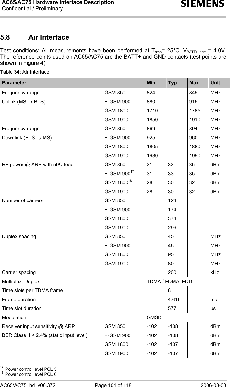
![AC65/AC75 Hardware Interface Description Confidential / Preliminary s AC65/AC75_hd_v00.372 Page 79 of 118 2006-08-03 4.1 Antenna Diagnostic The antenna diagnostic allows the customer to check the presence and the connection status of the antenna by using the AT^SAD command. A description of the AT^SAD command can be found in [1]. To properly detect the antenna and verify its connection status the antenna feed point must have a DC resistance RANT of 9kΩ (±3kΩ). Any lower or higher resistance from 1kΩ to 6kΩ or 12kΩ to 40k gives an undefined result. A positive or negative voltage drop (referred to as Vdisturb) on the ground line may occur without having any impact on the measuring procedure and the measuring result. A peak deviation (Vdisturb ) of ≤ 0.8V from ground is acceptable. Vdisturb (peak) = ± 0.8V (maximum); fdisturb = 0Hz … 5kHz Waveform: DC, sinus, square-pulse, peak-pulse (width = 100µs) Rdisturb = 5 Figure 38: Resistor measurement used for antenna detection Table 18: Values of the AT^SAD parameter <diag> and their meaning Antenna connection status indicated by AT^SAD <diag> Equivalent ranges Normal operation, antenna connected (resistance at feed point as required) <diag>=0 RANT = 6kΩ…12kΩ Antenna connector short-circuited to GND <diag>=1 RANT = 0...1kΩ Antenna connector is short-circuited to the supply voltage of the host application, for example the vehicle’s on-board power supply voltage <diag>=2 max. 36V Antenna not properly connected, or resistance at antenna feed point wrong or not present <diag>=3 RANT = 40kΩ...Ω Antenna connectorAC759k±3kExternal antennaVdisturb5 Ohm](https://usermanual.wiki/THALES-DIS-AlS-Deutschland/AC75/User-Guide-690611-Page-79.png)
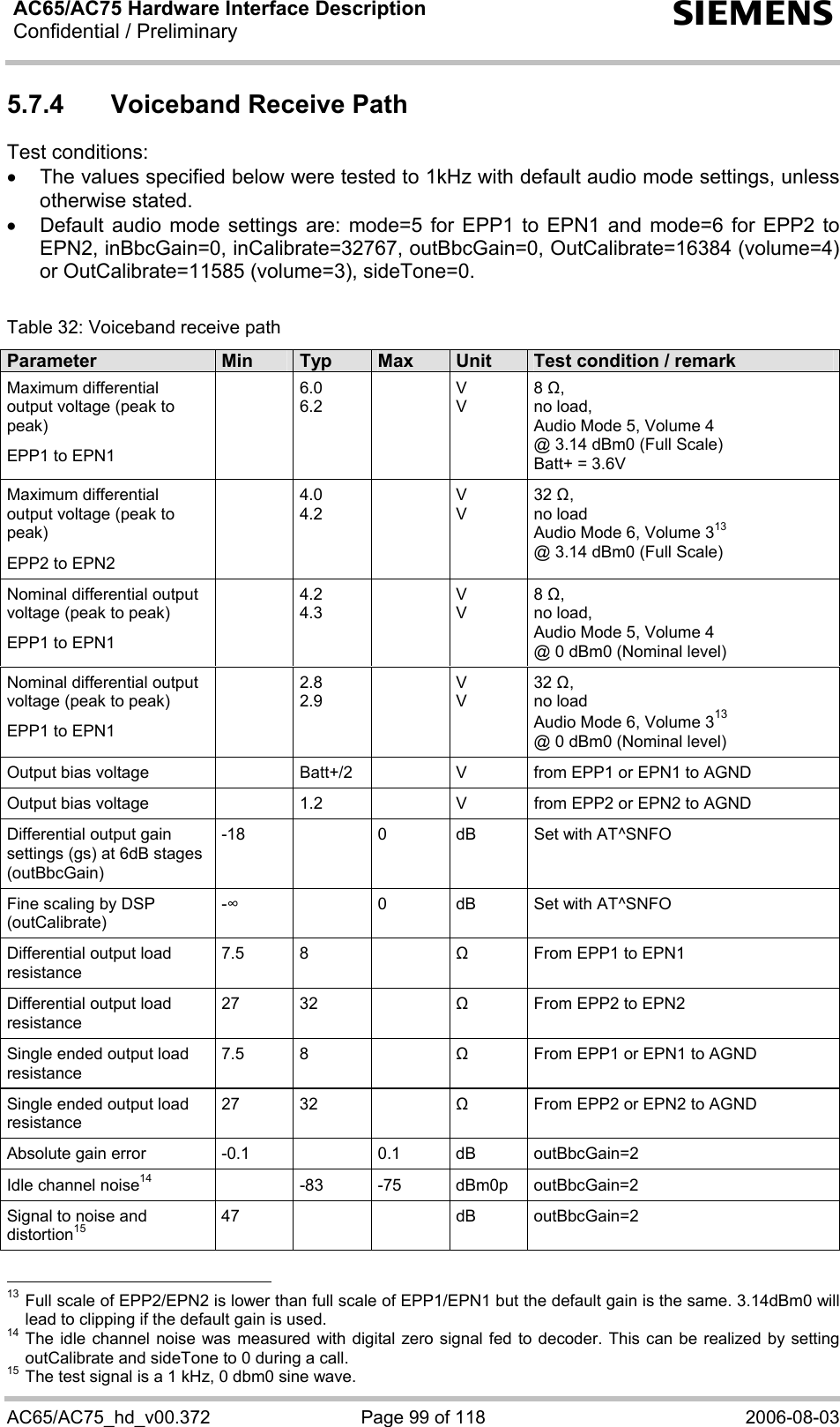
![AC65/AC75 Hardware Interface Description Confidential / Preliminary s AC65/AC75_hd_v00.372 Page 96 of 118 2006-08-03 5.7 Electrical Characteristics of the Voiceband Part 5.7.1 Setting Audio Parameters by AT Commands The audio modes 2 to 6 can be adjusted according to the parameters listed below. Each audio mode is assigned a separate set of parameters. Table 30: Audio parameters adjustable by AT command Parameter Influence to Range Gain range Calculation inBbcGain MICP/MICN analogue amplifier gain of baseband controller before ADC 0...7 0...42dB 6dB steps inCalibrate Digital attenuation of input signal after ADC 0...32767 -...0dB 20 * log (inCalibrate/32768) outBbcGain EPP/EPN analogue output gain of baseband controller after DAC 0...3 0...-18dB 6dB steps outCalibrate[n] n = 0...4 Digital attenuation of output signal after speech decoder, before summation of sidetone and DAC Present for each volume step[n] 0...32767 -...+6dB 20 * log (2 * outCalibrate[n]/ 32768) sideTone Digital attenuation of sidetone Is corrected internally by outBbcGain to obtain a constant sidetone independent of output volume 0...32767 -...0dB 20 * log (sideTone/ 32768) Note: The parameters outCalibrate and sideTone accept also values from 32768 to 65535. These values are internally truncated to 32767.](https://usermanual.wiki/THALES-DIS-AlS-Deutschland/AC75/User-Guide-690611-Page-96.png)
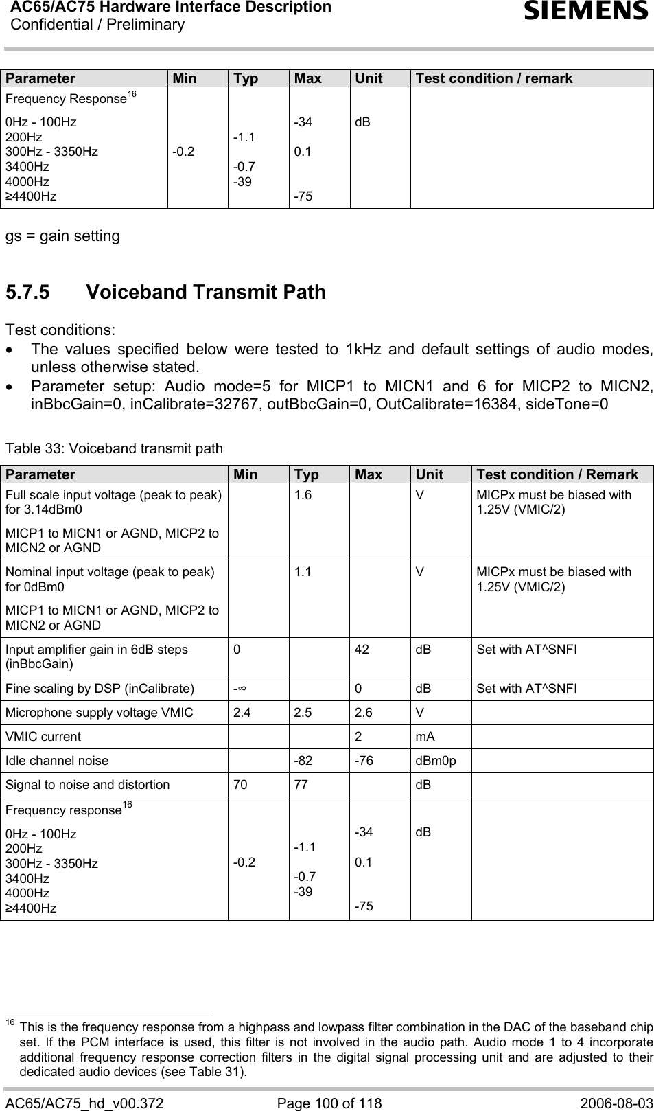
![AC65/AC75 Hardware Interface Description Confidential / Preliminary s AC65/AC75_hd_v00.372 Page 97 of 118 2006-08-03 5.7.2 Audio Programming Model The audio programming model shows how the signal path can be influenced by varying the AT command parameters. The parameters inBbcGain and inCalibrate can be set with AT^SNFI. All the other parameters are adjusted with AT^SNFO. Figure 41: Audio programming model <mic>MicrophonefeedingADSpeechcoder<sideTone>MIC1MIC2ADSpeechdecoderTXDDAIRXDDAI8OhmsEP1EP232 OhmsGSM module<ep>VMIC<io><inBbcGain> <inCalibrate><outCalibrate [n]><outBbcGain>AT parameters are given in brackets <...> and marked red and italic.](https://usermanual.wiki/THALES-DIS-AlS-Deutschland/AC75/User-Guide-690611-Page-97.png)
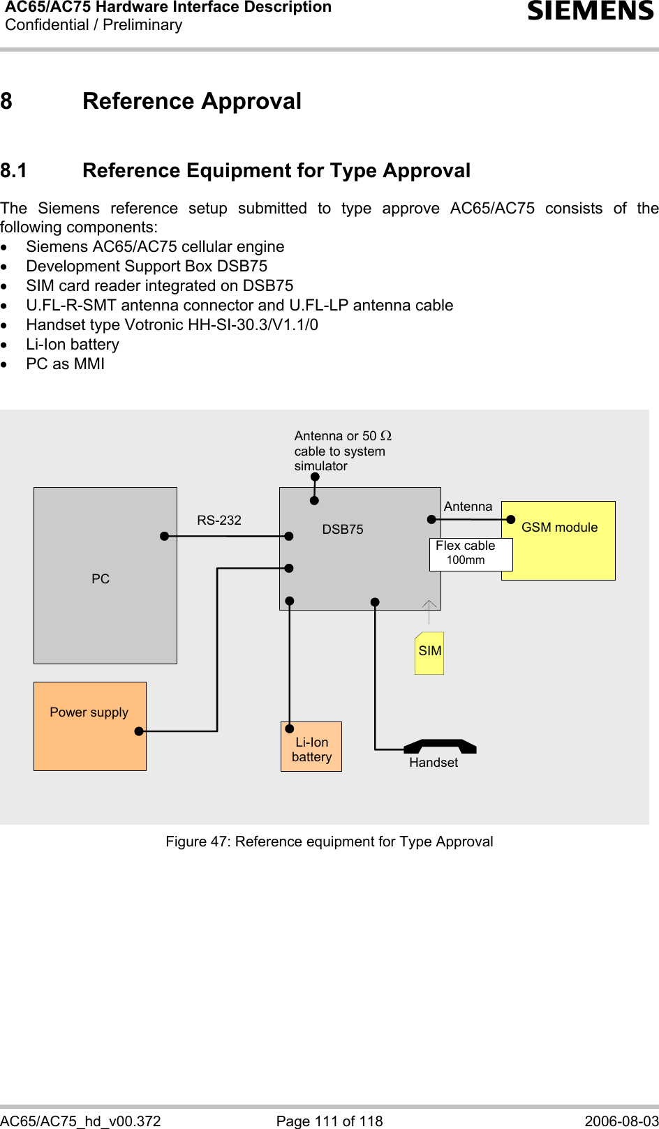
![AC65/AC75 Hardware Interface Description Confidential / Preliminary s AC65/AC75_hd_v00.372 Page 112 of 118 2006-08-03 8.2 Compliance with FCC Rules and Regulations The FCC Equipment Authorization Certification for the Siemens reference application described in Chapter 8.1 will be registered under the following identifiers: FCC identifier QIPAC65 IC: 267W-AC65 granted to Siemens AG and FCC identifier QIPAC75 IC: 267W-AC75 granted to Siemens AG. Manufacturers of mobile or fixed devices incorporating AC65/AC75 modules are authorized to use the FCC Grants and IC Certificates of the AC65/AC75 modules for their own final products according to the conditions referenced in these documents. In this case, the FCC label of the module shall be visible from the outside, or the host device shall bear a second label stating “Contains FCC ID QIP AC65” resp. “Contains FCC ID QIPAC75”. IMPORTANT: Manufacturers of portable applications incorporating AC65/AC75 modules are required to have their final product certified and apply for their own FCC Grant and IC Certificate related to the specific portable mobile. This is mandatory to meet the SAR requirements for portable mobiles (see Chapter 1.3.1 for detail). Changes or modifications not expressly approved by the party responsible for compliance could void the user’s authority to operate the equipment. If the final product is not approved for use in U.S. territories the application manufacturer shall take care that the 850 MHz and 1900 MHz frequency bands be deactivated and that band settings be inaccessible to end users. If these demands are not met (e.g. if the AT interface is accessible to end users), it is the responsibility of the application manufacturer to always ensure that the application be FCC approved regardless of the country it is marketed in. The frequency bands can be set using the command AT^SCFG="Radio/Band"[,<rbp>][, <rba>]. A detailed command description can be found in [1].](https://usermanual.wiki/THALES-DIS-AlS-Deutschland/AC75/User-Guide-690611-Page-112.png)