THALES DIS AlS Deutschland EHS6T Gemalto EHS6 Terminal User Manual hid
Gemalto M2M GmbH Gemalto EHS6 Terminal hid
Contents
- 1. User Manual
- 2. user manual
User Manual
M2M.GEMALTO.COM
Cinterion® Java Terminals
Hardware Interface Description
Version: 02
DocId: EHSxT_BGS5T_HID_v02

GENERAL NOTE
THE USE OF THE PRODUCT INCLUDING THE SOFTWARE AND DOCUMENTATION (THE "PROD-
UCT") IS SUBJECT TO THE RELEASE NOTE PROVIDED TOGETHER WITH PRODUCT. IN ANY
EVENT THE PROVISIONS OF THE RELEASE NOTE SHALL PREVAIL. THIS DOCUMENT CONTAINS
INFORMATION ON GEMALTO M2M PRODUCTS. THE SPECIFICATIONS IN THIS DOCUMENT ARE
SUBJECT TO CHANGE AT GEMALTO M2M'S DISCRETION. GEMALTO M2M GMBH GRANTS A NON-
EXCLUSIVE RIGHT TO USE THE PRODUCT. THE RECIPIENT SHALL NOT TRANSFER, COPY,
MODIFY, TRANSLATE, REVERSE ENGINEER, CREATE DERIVATIVE WORKS; DISASSEMBLE OR
DECOMPILE THE PRODUCT OR OTHERWISE USE THE PRODUCT EXCEPT AS SPECIFICALLY
AUTHORIZED. THE PRODUCT AND THIS DOCUMENT ARE PROVIDED ON AN "AS IS" BASIS ONLY
AND MAY CONTAIN DEFICIENCIES OR INADEQUACIES. TO THE MAXIMUM EXTENT PERMITTED
BY APPLICABLE LAW, GEMALTO M2M GMBH DISCLAIMS ALL WARRANTIES AND LIABILITIES.
THE RECIPIENT UNDERTAKES FOR AN UNLIMITED PERIOD OF TIME TO OBSERVE SECRECY
REGARDING ANY INFORMATION AND DATA PROVIDED TO HIM IN THE CONTEXT OF THE DELIV-
ERY OF THE PRODUCT. THIS GENERAL NOTE SHALL BE GOVERNED AND CONSTRUED
ACCORDING TO GERMAN LAW.
Copyright
Transmittal, reproduction, dissemination and/or editing of this document as well as utilization of its con-
tents and communication thereof to others without express authorization are prohibited. Offenders will be
held liable for payment of damages. All rights created by patent grant or registration of a utility model or
design patent are reserved.
Copyright © 2014, Gemalto M2M GmbH, a Gemalto Company
Trademark Notice
Gemalto, the Gemalto logo, are trademarks and service marks of Gemalto and are registered in certain
countries. Microsoft and Windows are either registered trademarks or trademarks of Microsoft Corpora-
tion in the United States and/or other countries. All other registered trademarks or trademarks mentioned
in this document are property of their respective owners.
EHSxT_BGS5T_HID_v02 2014-08-05
Confidential / Preliminary
Cinterion® Java Terminals Hardware Interface Description
2
Page 2 of 70
Document Name: Cinterion® Java Terminals Hardware Interface Description
Version: 02
Date: 2014-08-05
DocId: EHSxT_BGS5T_HID_v02
Status Confidential / Preliminary

Cinterion® Java Terminals Hardware Interface Description
Contents
115
EHSxT_BGS5T_HID_v02 2014-08-05
Confidential / Preliminary
Page 3 of 70
Contents
0 Document History ...................................................................................................... 7
1 Introduction ................................................................................................................. 8
1.1 Related Documents ........................................................................................... 9
1.2 Terms and Abbreviations................................................................................... 9
1.3 Regulatory and Type Approval Information ..................................................... 11
1.3.1 Directives and Standards.................................................................... 11
1.3.2 Safety Precautions.............................................................................. 14
1.4 Product Label................................................................................................... 16
2 Product Concept ....................................................................................................... 17
2.1 Key Features at a Glance ................................................................................ 17
3 Interface Description ................................................................................................ 20
3.1 Overview.......................................................................................................... 20
3.2 Block Diagram.................................................................................................. 21
3.3 Terminal Circuit................................................................................................ 22
3.4 Operating Modes ............................................................................................. 23
3.5 RS-232 Interface.............................................................................................. 24
3.5.1 9-Pole D-sub Connector ..................................................................... 24
3.6 USB Interface................................................................................................... 25
3.7 Weidmueller GPIO Interface............................................................................ 25
3.8 Power Supply................................................................................................... 29
3.8.1 Turn Java Terminals on ...................................................................... 30
3.8.2 Reset Java Terminals ......................................................................... 30
3.8.3 Turn Java Terminals off ...................................................................... 30
3.8.4 Disconnecting power supply ............................................................... 31
3.9 Automatic thermal shutdown............................................................................ 32
3.10 Hardware Watchdog ........................................................................................ 32
3.11 RTC.................................................................................................................. 32
3.12 SIM Interface.................................................................................................... 33
3.13 Status LEDs..................................................................................................... 34
3.14 RF Antenna Interface....................................................................................... 35
4 Electrical and Environmental Characteristics........................................................ 36
4.1 Absolute Maximum Ratings ............................................................................. 36
4.2 Operating Temperatures.................................................................................. 37
4.3 Storage Conditions .......................................................................................... 38
4.4 Electrical Specifications of the Application Interface........................................ 39
4.4.1 On/Off Control..................................................................................... 39
4.4.2 RS-232 Interface................................................................................. 39
4.4.3 USB Interface...................................................................................... 39
4.4.4 Weidmueller GPIO Interface............................................................... 40
4.5 Power Supply Ratings...................................................................................... 41
4.6 Antenna Interface............................................................................................. 43

Cinterion® Java Terminals Hardware Interface Description
Contents
115
EHSxT_BGS5T_HID_v02 2014-08-05
Confidential / Preliminary
Page 4 of 70
5 Mechanics, Mounting and Packaging ..................................................................... 45
5.1 Mechanical Dimensions................................................................................... 45
5.2 Mounting the Java Terminals........................................................................... 47
5.3 Packaging ........................................................................................................ 48
6 Full Type Approval.................................................................................................... 49
6.1 Gemalto M2M Reference Setup ...................................................................... 49
6.2 Restrictions ...................................................................................................... 50
6.3 CE Conformity.................................................................................................. 50
6.4 EMC................................................................................................................. 50
6.5 Compliance with FCC and IC Rules and Regulations ..................................... 51
7 List of Parts and Accessories.................................................................................. 53
8 Appendix A: (Hardware) Watchdog......................................................................... 54
8.1 Reset Conditions.............................................................................................. 54
8.1.1 Reset stages....................................................................................... 55
8.1.2 Reset Delay ........................................................................................ 55
8.2 Restart Conditions ........................................................................................... 55
8.3 Configuration via ASC0 Interface..................................................................... 56
8.3.1 Command Specification...................................................................... 56
8.4 Configuration via I2C Interface ......................................................................... 65
8.4.1 Command Specification...................................................................... 65

Cinterion® Java Terminals Hardware Interface Description
Figures
5
EHSxT_BGS5T_HID_v02 2014-08-05
Confidential / Preliminary
Page 5 of 70
Figures
Figure 1: Sample Java Terminal label (BGS5T USB) .................................................... 16
Figure 2: Java Terminals 3D view.................................................................................. 20
Figure 3: Block diagram ................................................................................................. 21
Figure 4: Java Terminals circuit block diagram.............................................................. 22
Figure 5: Pin assignment RS-232 (D-sub 9-pole female)............................................... 24
Figure 6: EHS5T RS485: Weidmueller connectors (8-pin and 12-pin)........................... 25
Figure 7: EHS6T USB: Weidmueller connectors (8-pin and 12-pin) .............................. 26
Figure 8: BGS5T USB: Weidmueller connectors (8-pin and 12-pin).............................. 26
Figure 9: 6-pole Western jack for power supply, ignition, reset, typical connection....... 29
Figure 10: SIM interface................................................................................................... 33
Figure 11: Status LED...................................................................................................... 34
Figure 12: Antenna connector.......................................................................................... 35
Figure 13: Java Terminals 3D overview........................................................................... 45
Figure 14: Java Terminals mechanical dimensions ......................................................... 46
Figure 15: Mounting the Java Terminals.......................................................................... 47
Figure 16: Reference equipment for approval.................................................................. 49
Figure 17: Hardware watchdog ........................................................................................ 54
Figure 18: Write data to address register......................................................................... 68
Figure 19: Read data from address register..................................................................... 69

Cinterion® Java Terminals Hardware Interface Description
Tables
6
EHSxT_BGS5T_HID_v02 2014-08-05
Confidential / Preliminary
Page 6 of 70
Tables
Table 1: Cinterion® Java Terminals overview ................................................................. 8
Table 2: Terms and abbreviations................................................................................... 9
Table 3: Directives ........................................................................................................ 11
Table 4: Standards of North American type approval ................................................... 11
Table 5: Standards of European type approval............................................................. 11
Table 6: Requirements of quality .................................................................................. 12
Table 7: Standards of the Ministry of Information Industry of the
People’s Republic of China............................................................................. 13
Table 8: Toxic or hazardous substances or elements with defined concentration
limits................................................................................................................ 13
Table 9: Java Terminals label information .................................................................... 16
Table 10: Overview of operating modes ......................................................................... 23
Table 11: 9-pole D-sub (female) RS-232 ........................................................................ 24
Table 12: Weidmueller pin availability............................................................................. 27
Table 13: Female 6-pole Western plug for power supply, ignition, power down............. 29
Table 14: Allowed maximum antenna gain (including cable loss)................................... 35
Table 15: Absolute maximum ratings.............................................................................. 36
Table 16: Operating supply voltage for Java Terminals.................................................. 36
Table 17: Board temperature of Java module................................................................. 37
Table 18: Storage conditions .......................................................................................... 38
Table 19: On/Off control line specifications..................................................................... 39
Table 20: RS-232 interface specifications....................................................................... 39
Table 21: Weidmueller GPIO interface specifications (requirements) ............................ 40
Table 22: Power supply specifications............................................................................ 41
Table 23: RF Antenna interface GSM / UMTS................................................................ 43
Table 24: List of parts and accessories........................................................................... 53
Table 25: Address register for I2C commands ................................................................ 66
Table 26: I2C status result codes .................................................................................... 67
Cinterion® Java Terminals Hardware Interface Description
0 Document History
7
EHSxT_BGS5T_HID_v02 2014-08-05
Confidential / Preliminary
Page 7 of 70
0 Document History
Preceding document: "Cinterion® Java Terminals Hardware Interface Description" Version 01
New document: "Cinterion® Java Terminals Hardware Interface Description" Version 02
New document: "Cinterion® Java Terminals Hardware Interface Description" Version 01
Chapter What is new
1.4 Revised product label shown in Figure 1.
3.7 Revised section with regard to the Weidmueller pin availability.
4.1 Completed Table 15 giving absolute maximum ratings.
4.2 Added remarks on board temperature.
4.5 Revised and completed section listing power supply ratings.
6.3 Added CE conformity mark.
6.5 Revised section to include notes for IC (also in the Frensh language).
8Revised and updated Appendix A: (Hardware) Watchdog.
Chapter What is new
--- Initial document setup.
Cinterion® Java Terminals Hardware Interface Description
1 Introduction
16
EHSxT_BGS5T_HID_v02 2014-08-05
Confidential / Preliminary
Page 8 of 70
1 Introduction
This document1 describes the hardware of the Cinterion® Java Terminals. The Java Terminals
come in three variants depending on the included Cinterion® module and the available interfac-
es:
•EHS5T RS485 contains a Cinterion® EHS5-E module and implements a USB 2.0 interface
with a USB-B connector as well as a 6-pole Western jack as plug-in power supply connec-
tor. Via a Weidmüller GPIO connectors it also implements a RS-485 interface including
power supply and ignition line.
•EHS6T USB contains a Cinterion® EHS6 module and implements a USB 2.0 interface with
a USB-B connector and also a V.24 / V.28 RS-232 interface with a D-sub 9-pole female
socket as well as a 6-pole Western jack as plug-in power supply connector.
•BGS5T USB contains a Cinterion® BGS5 module and implements a USB 2.0 interface with
a USB-B connector and also a V.24 / V.28 RS-232 interface with a D-sub 9-pole female
socket as well as a 6-pole Western jack as plug-in power supply connector.
Wherever necessary and appropriate this document distinguishes between these three vari-
ants.
Table 1 gives a short overview of the available interfaces for the different Java Terminals.
The scope of this document includes interface specifications, electrical as well as mechanical
characteristics of the Java Terminals. It specifies standards pertaining to wireless applications
and outlines requirements that must be adhered to for successful product design. The Java
Terminals are compact GSM/UMTS modems for the transfer of data in GSM/UMTS networks.
Industrial standard interfaces and an integrated SIM card reader allow using the Java Termi-
nals easily as GSM/GPRS/UMTS terminals.
1. The document is effective only if listed in the appropriate Release Notes as part of the technical
documentation delivered with your Gemalto M2M product.
Table 1: Cinterion® Java Terminals overview
Module/Interface EHS5T RS485 EHS6T USB BGS5T USB
Cinterion® module EHS5-E EHS6 BGS5
RS-232 (Sub-D) -
USB (USB-B)
Weidmüller connector
(GPIOs, SPI, I2C, RS-485)
(no RS-485) (no RS-485,
no SPI)
Power supply (RJ-11)
RF antenna

Cinterion® Java Terminals Hardware Interface Description
1.1 Related Documents
16
EHSxT_BGS5T_HID_v02 2014-08-05
Confidential / Preliminary
Page 9 of 70
1.1 Related Documents
[1] AT Command Set for your Java Terminal product
[2] Release Notes for your Java Terminal product
To visit the Gemalto M2M GmbH Website please use the following link:
http://m2m.gemalto.com
1.2 Terms and Abbreviations
Table 2: Terms and abbreviations
Abbreviation Description
ARP Antenna Reference Point
ATC AT Command
BTS Base Transceiver Station
CB Cell Broadcast
CODEC Coder-Decoder
DCE Data Circuit terminating Equipment
DSR Data Set Ready
DTR Data Terminal Ready
EFR Enhanced Full Rate
EGSM Enhanced GSM
EMC Electromagnetic Compatibility
ESD Electrostatic Discharge
ETS European Telecommunication Standard
FDMA Frequency Division Multiple Access
G.C.F. GSM Conformity Forum
GSM Global Standard for Mobile Communication
HW Hardware
IC Integrated Circuit
IF Intermediate Frequency
IMEI International Mobile Equipment Identifier
I/O Input/ Output
IGT Ignition
ISO International Standards Organization
ITU International Telecommunications Union
kbps kbits per second
LVD Low voltage Directive

Cinterion® Java Terminals Hardware Interface Description
1.2 Terms and Abbreviations
16
EHSxT_BGS5T_HID_v02 2014-08-05
Confidential / Preliminary
Page 10 of 70
Mbps Mbits per second
MMI Machine Machine Interface
MO Mobile Originated
MS Mobile Station
MT Mobile Terminated
NC Not Connected
NTC Negative Temperature Coefficient
PA Power Amplifier
PCB Printed Circuit Board
PCM Pulse Code Modulation
PCS Personal Communication System
PD Power Down
PDU Protocol Data Unit
R&TTE Radio and Telecommunication Terminal Equipment
RF Radio frequency
RI Ring Indication
RX Receive direction
SIM Subscriber Identification Module
SMS Short Message Service
SW Software
TDD Time Division Duplex
TDMA Time Division Multiple Access
TX Transmit direction
UART Universal Asynchronous Receiver and Transmitter
Table 2: Terms and abbreviations
Abbreviation Description
Cinterion® Java Terminals Hardware Interface Description
1.3 Regulatory and Type Approval Information
16
EHSxT_BGS5T_HID_v02 2014-08-05
Confidential / Preliminary
Page 11 of 70
1.3 Regulatory and Type Approval Information
1.3.1 Directives and Standards
Java Terminals have been designed to comply with the directives and standards listed below1.
1. Standards of North American type approval do not apply to EHS5T RS485, 3G/WCDMA related
standards do not apply to BGS5T USB.
Table 3: Directives
99/05/EC Directive of the European Parliament and of the council of 9 March 1999
on radio equipment and telecommunications terminal equipment and the
mutual recognition of their conformity (in short referred to as R&TTE Direc-
tive 1999/5/EC).
The product is labeled with the CE conformity mark
2002/95/EC (RoHS 1)
2011/65/EC (RoHS 2) Directive of the European Parliament and of the Council of
27 January 2003 (and revised on 8 June 2011) on the
restriction of the use of certain hazardous substances in
electrical and electronic equipment (RoHS)
2002/96/EC Directive of the European Parliament and of the Council on waste electri-
cal and electronic equipment (WEEE)
2003/108/EC Directive of the European Parliament and of the Council of 8 December
2003 amending directive 2002/96/ec on waste electrical and electronic
equipment (WEEE)
Table 4: Standards of North American type approval
CFR Title 47 “Code of Federal Regulations, Part 15 B, Part 22 and Part 24 (Telecom-
munications, PCS)”; US Equipment Authorization FCC
OET Bulletin 65
(Edition 97-01) Evaluating Compliance with FCC Guidelines for Human Exposure to
Radiofrequency Electromagnetic Fields
UL 60 950-1 Product Safety Certification (Safety requirements)
NAPRD.03 V5.15 “Overview of PCS Type certification review board
Mobile Equipment Type Certification and IMEI control”
PCS Type Certification Review board (PTCRB)
RSS102 (Issue 4)
RSS132 (Issue 3)
RSS133 (Issue 6)
Canadian Standard
IEEE Std. C95.1-1999 IEEE Standard for Safety Levels with Respect to Human Exposure to
Radio Frequency Electromagnetic Fields, 3 kHz to 300 GHz
Table 5: Standards of European type approval
3GPP TS 51.010-1 “Digital cellular telecommunications system (Phase 2); Mobile Station
(MS) conformance specification”
ETSI EN 301 511 V9.0.2 Candidate Harmonized European Standard (Telecommunications series)
Global System for Mobile communications (GSM); Harmonized standard
for mobile stations in the GSM 900 and DCS 1800 bands covering essen-
tial requirements under article 3.2 of the R&TTE directive (1999/5/EC)
(GSM 13.11 version 7.0.1 Release 1998)
GCF-CC V3.49 Global Certification Forum - Certification Criteria
Cinterion® Java Terminals Hardware Interface Description
1.3 Regulatory and Type Approval Information
16
EHSxT_BGS5T_HID_v02 2014-08-05
Confidential / Preliminary
Page 12 of 70
ETSI EN 301 489-1
V1.9.2 Candidate Harmonized European Standard (Telecommunications series)
Electro Magnetic Compatibility and Radio spectrum Matters (ERM); Elec-
tro Magnetic Compatibility (EMC) standard for radio equipment and ser-
vices; Part 1: Common Technical Requirements
ETSI EN 301 489-7
V1.3.1 Candidate Harmonized European Standard (Telecommunications series)
Electro Magnetic Compatibility and Radio spectrum Matters (ERM); Elec-
tro Magnetic Compatibility (EMC) standard for radio equipment and ser-
vices; Part 7: Specific conditions for mobile and portable radio and
ancillary equipment of digital cellular radio telecommunications systems
(GSM and DCS)
ETSI EN 301 489-24
V1.5.1 Electromagnetic Compatibility and Radio spectrum Matters (ERM); Elec-
tromagnetic Compatibility (EMC) standard for radio equipment and ser-
vices; Part 24: Specific conditions for IMT-2000 CDMA Direct Spread
(UTRA) for Mobile and portable (UE) radio and ancillary equipment
ETSI EN 301 908-01
V5.2.1 Electromagnetic compatibility and Radio spectrum Matters (ERM); Base
Stations (BS) and User Equipment (UE) for IMT-2000 Third Generation
cellular networks; Part 1: Harmonized EN for IMT-2000, introduction and
common requirements of article 3.2 of the R&TTE Directive
ETSI EN 301 908-02
V5.2.1 Electromagnetic compatibility and Radio spectrum Matters (ERM); Base
Stations (BS) and User Equipment (UE) for IMT-2000 Third Generation
cellular networks; Part 2: Harmonized EN for IMT-2000, CDMA Direct
Spread (UTRA FDD) (UE) covering essential requirements of article 3.2 of
the R&TTE Directive
EN 62311-2008 Assessment of electronic and electrical equipment related to human expo-
sure restrictions for electromagnetic fields (0 Hz - 300 GHz)
EN 60950-1 (2006)+
A11:2009+A1:2010+
AC:2011+A12:2011
Safety of information technology equipment
Table 6: Requirements of quality
IEC 60068 Environmental testing
DIN EN 60529 IP codes
Table 5: Standards of European type approval
Cinterion® Java Terminals Hardware Interface Description
1.3 Regulatory and Type Approval Information
16
EHSxT_BGS5T_HID_v02 2014-08-05
Confidential / Preliminary
Page 13 of 70
Table 8: Toxic or hazardous substances or elements with defined concentration limits
Table 7: Standards of the Ministry of Information Industry of the People’s Republic of China
SJ/T 11363-2006 “Requirements for Concentration Limits for Certain Hazardous Sub-
stances in Electronic Information Products” (2006-06).
SJ/T 11364-2006 “Marking for Control of Pollution Caused by Electronic
Information Products” (2006-06).
According to the “Chinese Administration on the Control
of Pollution caused by Electronic Information Products”
(ACPEIP) the EPUP, i.e., Environmental Protection Use
Period, of this product is 20 years as per the symbol
shown here, unless otherwise marked. The EPUP is valid only as long as
the product is operated within the operating limits described in the Hard-
ware Interface Description.
Please see Table 1.3.2 for an overview of toxic or hazardous substances
or elements that might be contained in product parts in concentrations
above the limits defined by SJ/T 11363-2006.
Cinterion® Java Terminals Hardware Interface Description
1.3 Regulatory and Type Approval Information
16
EHSxT_BGS5T_HID_v02 2014-08-05
Confidential / Preliminary
Page 14 of 70
1.3.2 Safety Precautions
The following safety precautions must be observed during all phases of the operation, usage,
service or repair of any cellular terminal or mobile incorporating Java Terminals. Manufacturers
of the cellular terminal are advised to convey the following safety information to users and op-
erating personnel and incorporate these guidelines into all manuals supplied with the product.
Failure to comply with these precautions violates safety standards of design, manufacture and
intended use of the product. Gemalto M2M GmbH assumes no liability for customer’s failure to
comply with these precautions.
When in hospitals or other health care facilities, observe the restrictions on the use
of mobiles. Switch off the cellular terminal or mobile if to be instructed to do so by
the guidelines posted in sensitive areas. Medical equipment may be sensitive to RF
energy.
The operation of cardiac pacemakers, other implanted medical equipment and
hearing aids can be affected by interference from cellular terminals or mobiles
placed close to the device. If in doubt about potential danger, contact the physician
or the manufacturer of the device to verify that the equipment is properly shielded.
Pacemaker patients are advised to keep their hand-held mobile away from the
pacemaker, while it is on. This personal subgroup always should check the distance
to the mobile.
Switch off the cellular terminal or mobile before boarding an aircraft. Make sure it
cannot be switched on inadvertently. The operation of wireless appliances in an air-
craft is forbidden to prevent interference with communications systems. Failure to
observe these instructions may lead to the suspension or denial of cellular services
to the offender, legal action, or both.
Check the local and actual laws about these themes.
Do not operate the cellular terminal or mobile in the presence of flammable gases
or fumes. Switch off the cellular terminal when you are near petrol stations, fuel
depots, chemical plants or where blasting operations are in progress. Operation of
any electrical equipment in potentially explosive atmospheres can constitute a
safety hazard.
Your cellular terminal or mobile receives and transmits radio frequency energy while
switched on. Remember that interference can occur if it is used close to TV sets,
radios, computers or inadequately shielded equipment. Follow any special regula-
tions and always switch off the cellular terminal or mobile wherever forbidden, or
when you suspect that it may cause interference or danger.
Road safety comes first! Do not use a hand-held cellular terminal or mobile while
driving a vehicle unless it is securely mounted in a holder for speakerphone opera-
tion. Before making a call with a hand-held terminal or mobile park the vehicle.
Speakerphones must be installed by qualified personnel. Faulty installation or oper-
ation can constitute a safety hazard.
Check the actual and local laws about these themes.
Cinterion® Java Terminals Hardware Interface Description
1.3 Regulatory and Type Approval Information
16
EHSxT_BGS5T_HID_v02 2014-08-05
Confidential / Preliminary
Page 15 of 70
IMPORTANT!
Cellular terminals or mobiles operate using radio signals and cellular networks. In
that case connections cannot be guaranteed at all times under all conditions. There-
fore, you should never rely solely upon any wireless device for essential communi-
cations, for example emergency calls.
Remember, in order to make calls or receive calls the cellular terminal or mobile
must be switched on in a service area with adequate cellular signal strength.
Some networks do not allow for emergency calls if certain network services or
phone features are in use (e.g. lock functions, fixed dialing etc.). You may need to
deactivate those features before you can make an emergency call.
Some networks require a valid SIM card to be properly inserted in the cellular ter-
minal or mobile.
If a power supply unit is used to supply the device it must meet the demands placed
on SELV circuits in accordance with EN60950. The maximum permissible connec-
tion length between the device and the supply source should not exceed 3m.
According to the guidelines for human exposure to radio frequency energy, an
antenna connected to the FME jack of the device should be placed at least 20cm
away from human bodies.
Cinterion® Java Terminals Hardware Interface Description
1.4 Product Label
16
EHSxT_BGS5T_HID_v02 2014-08-05
Confidential / Preliminary
Page 16 of 70
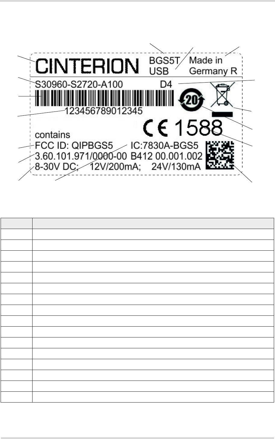
1.4 Product Label
The label fixed to the bottom of a Java Terminal comprises the following information.
Figure 1: Sample Java Terminal label (BGS5T USB)
Table 9: Java Terminals label information
No. Information
1 Cinterion logo
2 Product name
3 Product variant
4 Marking "Made in Germany"
5 Product ordering number
6 Barcode (Code128)
7 Product IMEI
8 Date code
9 WEEE symbol (see Table 3)
10 Chinese RoHS symbol (see Table 7)
11 CE logo with fixed notified body number (may be replaced for samples with "Not for sale")
12 FCC ID
13 IC ID
14 Manufacturer code
15 Power supply unit ratings
16 Manufacturer code (2D)
1
234
5
6
7
8
9
10
12
13
14
15 16
11

Cinterion® Java Terminals Hardware Interface Description
2 Product Concept
19
EHSxT_BGS5T_HID_v02 2014-08-05
Confidential / Preliminary
Page 17 of 70
2 Product Concept
2.1 Key Features at a Glance
Feature Implementation
General
Incorporates Cinterion®
Java module The Java module handles all signal and data processing within the Java
Terminals. Internal software runs the application interface and the complete
GSM/UMTS protocol stack.
Frequency bands EHS5T RS485 (with EHS5-E module):
GSM/GPRS/EDGE: Dual band GSM 900/1800MHz
UMTS/HSPA+: Dual band UMTS 900/2100MHz
EHS6T USB (with EHS6 module):
GSM/GPRS/EDGE: Quad band 850/900/1800/1900MHz
UMTS/HSPA+: Five band 800/850/900/1900/2100MHz
BGS5T USB (with BGS5 module):
GSM/GPRS: Quad band 850/900/1800/1900MHz
GSM class Small MS
Output power (according
to Release 99, V5)
depending on frequency
band supported by mod-
ule
Class 4 (+33dBm ±2dB) for EGSM850
Class 4 (+33dBm ±2dB) for EGSM900
Class 1 (+30dBm ±2dB) for GSM1800
Class 1 (+30dBm ±2dB) for GSM1900
Class E2 (+27dBm ± 3dB) for GSM 850 8-PSK
Class E2 (+27dBm ± 3dB) for GSM 900 8-PSK
Class E2 (+26dBm +3 /-4dB) for GSM 1800 8-PSK
Class E2 (+26dBm +3 /-4dB) for GSM 1900 8-PSK
Class 3 (+24dBm +1/-3dB) for UMTS 2100, WCDMA FDD BdI
Class 3 (+24dBm +1/-3dB) for UMTS 1900,WCDMA FDD BdII
Class 3 (+24dBm +1/-3dB) for UMTS 900, WCDMA FDD BdVIII
Class 3 (+24dBm +1/-3dB) for UMTS 850, WCDMA FDD BdV
Class 3 (+24dBm +1/-3dB) for UMTS 800, WCDMA FDD BdVI
The values stated above are maximum limits. According to Release 99, the
maximum output power in a multislot configuration may be lower. The nom-
inal reduction of maximum output power varies with the number of uplink
timeslots used and amounts to 3.0dB for 2Tx.
Power supply Single supply voltage 8V to 30V
Operating temperature Normal operation: -30°C to +85°C
Extended operation: -40°C to -30°C and +85°C to +90°C
Physical Dimensions: 113.5mm x 75mm x 25.5mm
(excluding antenna and serial interface connectors)
Weight: 120g (approx.)
RoHS, WEEE All hardware components are fully compliant with the EU RoHS and WEEE
Directives
HSPA features
3GPP Release 6,7
(EHSxT only) DL 7.2Mbps, UL 5.7Mbps
HSDPA Cat.8 / HSUPA Cat.6 data rates
Compressed mode (CM) supported according to 3GPP TS25.212

Cinterion® Java Terminals Hardware Interface Description
2.1 Key Features at a Glance
19
EHSxT_BGS5T_HID_v02 2014-08-05
Confidential / Preliminary
Page 18 of 70
UMTS features
3GPP Release 4
(EHSxT only) PS data rate – 384 kbps DL / 384 kbps UL
CS data rate – 64 kbps DL / 64 kbps UL
GSM / GPRS / EDGE features
Data transfer GPRS:
• Multislot Class 12
• Full PBCCH support
• Mobile Station Class B
• Coding Scheme 1 – 4
EGPRS (EHSxT only):
• Multislot Class 12
• EDGE E2 power class for 8 PSK
• Downlink coding schemes – CS 1-4, MCS 1-9
• Uplink coding schemes – CS 1-4, MCS 1-9
• SRB loopback and test mode B
• 8-bit, 11-bit RACH
• PBCCH support
• 1 phase/2 phase access procedures
• Link adaptation and IR
• NACC, extended UL TBF
• Mobile Station Class B
CSD:
• V.110, RLP, non-transparent
• 2.4, 4.8, 9.6, 14.4kbps
• USSD
SMS • Point-to-point MT and MO
• Cell broadcast
• Text and PDU mode
•
Software
AT commands Hayes 3GPP TS 27.007, TS 27.005, Gemalto M2M
Java™ Open Platform Java™ Open Platform with
• Java™ profile IMP-NG & CLDC 1.1 HI
• Secure data transmission via HTTPS/SSL
• Multi-threading programming and multi-application execution
Major benefits: seamless integration into Java applications, ease of pro-
gramming, no need for application microcontroller, extremely cost-efficient
hardware and software design – ideal platform for industrial GSM applica-
tions.
The memory space available for Java programs is around 10MB in the flash
file system and around 6MB RAM. Application code and data share the
space in the flash file system and in RAM.
SIM Application Toolkit SAT Release 99
TCP/IP stack Protocols: TCP server/client, UDP, HTTP, FTP, SMTP, POP3
Access by AT commands
Firmware update Upgradeable via serial or USB interface
Feature Implementation

Cinterion® Java Terminals Hardware Interface Description
2.1 Key Features at a Glance
19
EHSxT_BGS5T_HID_v02 2014-08-05
Confidential / Preliminary
Page 19 of 70
Interfaces
USB interfaces USB 2.0 Slave interface
RS232 RS-232 interface for AT commands and data:
• Supports RTS/CTS hardware handshake
• Supports software XON/XOFF flow control
• Multiplex ability according to GSM 07.10 Multiplexer protocol
• Baud rates from 1200bps to 230400bps
• Autobauding supported
Weidmueller connector 20-pin (8-pin and 12-pin) header with GPIO interface, external power sup-
ply, ADC, SPI, I²C and RS-485 option, depending on variant
Power connector 6-pole Western connector (female) for power supply, ignition, power down
signal
SIM card reader Supported SIM cards: 3V, 1.8V
Antenna Antenna connected via female SMA connector
Power on/off, Reset
Power on DTR line at RS-232 interface, IGT_IN line at power connector or watchdog
Power off Normal switch-off by AT^SMSO or external On/Off push button
Automatic switch-off in case of critical temperature conditions
Reset Orderly shutdown and reset by AT command
Emergency restart via RST_IN line at power connector or via watchdog
Special features
Real time clock Timer functions via AT commands
Phonebook SIM card and terminal
(Hardware) Watchdog Configurable watchdog to control module
Feature Implementation
Cinterion® Java Terminals Hardware Interface Description
3 Interface Description
35
EHSxT_BGS5T_HID_v02 2014-08-05
Confidential / Preliminary
Page 20 of 70
3 Interface Description
3.1 Overview
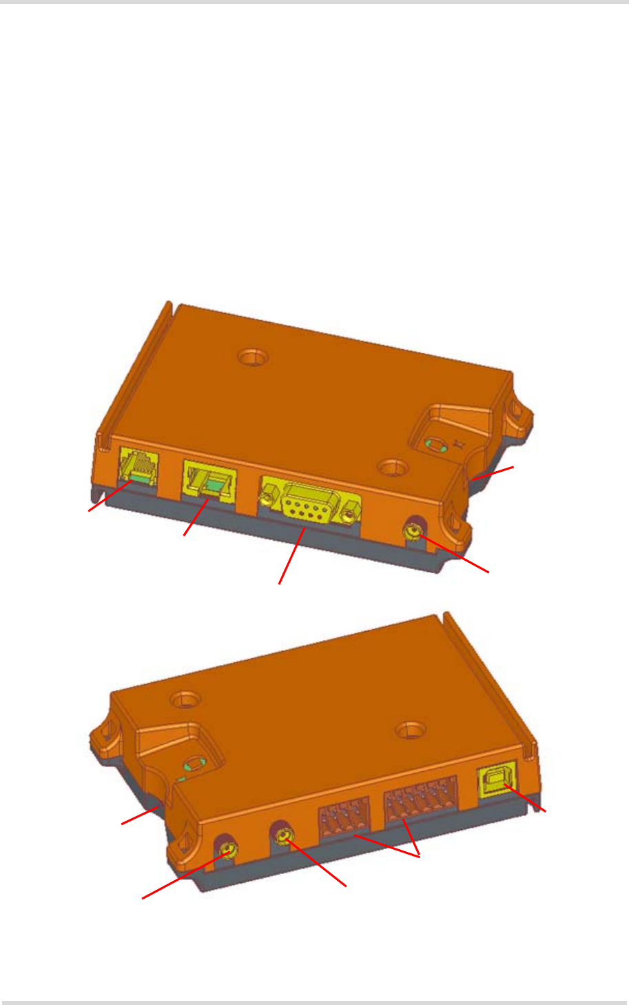
Java Terminals provide the following interfaces for power supply, antenna, SIM card and data
transfer:
• 6-pin Western connector (female) for power supply, ignition, power down signal
• SMA antenna connectors (female) for RF antenna and future Rx diversity or GPS antennas
• SIM card reader
• 9-pin (female) D-sub connector (RS-232 interface)
• 4-pin (female) USB-B connector
• 12-pin and 8-pin Weidmueller GPIO connectors (including RS-485)
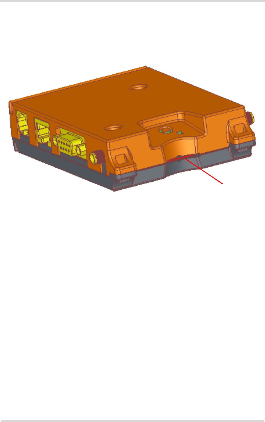
Figure 2: Java Terminals 3D view
GPS antenna SMA connector
D-sub socket (RS-232 interface)
Western jack for
USB connector
20-pin Weidmueller connector
SIM card reader
SIM card reader
(for future use,
RJ-45 Ethernet connector
(8-pin and 12-pin)
RF antenna SMA connector Rx diversity antenna SMA connector
(for future use; currently not available)
(for future use,
(not for EHS5T RS485)
power supply
currently not available)
currently not available)
Cinterion® Java Terminals Hardware Interface Description
3.2 Block Diagram
35
EHSxT_BGS5T_HID_v02 2014-08-05
Confidential / Preliminary
Page 21 of 70
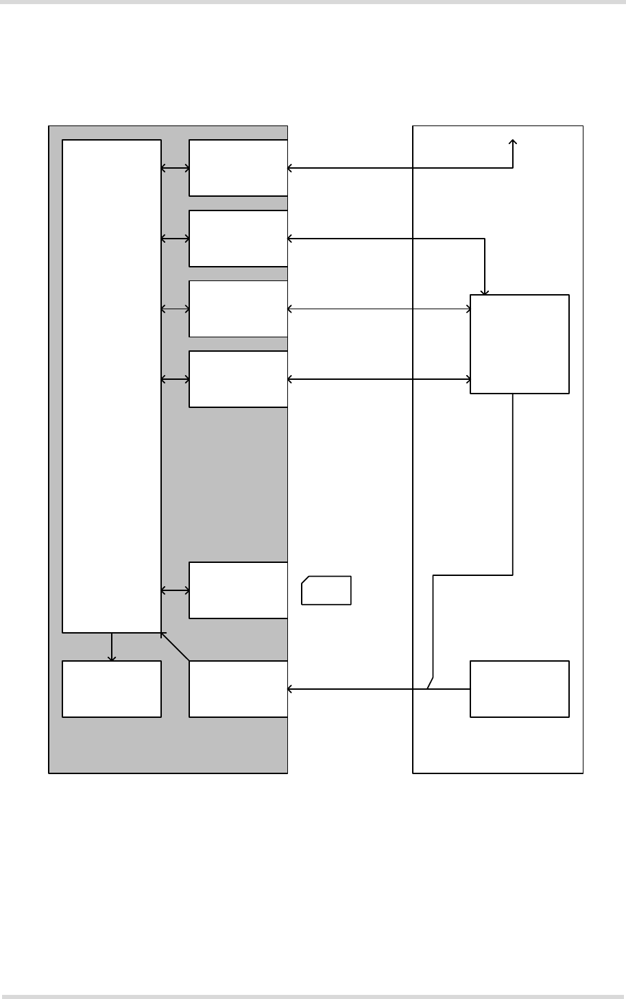
3.2 Block Diagram
Figure 3 shows a block diagram of a sample configuration that incorporates a Java Terminal
and typical accessories.
Figure 3: Block diagram
Java Terminal
Java
module
RS-232
driver
USB
SIM card
interface
Power regulation
RF antenna
interface
LEDs
RF antenna interface
Host
controller
Power supply
External application
Power supply
SIM
card
Antenna
IGT_IN
RST_IN
Weidmueller
GPIO
driver/interface
Not for EHS5T RS485

Cinterion® Java Terminals Hardware Interface Description
3.3 Terminal Circuit
35
EHSxT_BGS5T_HID_v02 2014-08-05
Confidential / Preliminary
Page 22 of 70
3.3 Terminal Circuit
Figure 4 shows a general Java Terminal block diagram that includes all variants. Not every
interface is available for all Terminal products.
Figure 4: Java Terminals circuit block diagram
D‐Sub9‐pin
Level‐
shifter
RS232interface
EMC
RS232driver
Batt+
SIMcard
holder
SIMcardinterface
CCxxx
EMC
Batt+
LED
green LED
yellow
LED drivers
LED
V180
SMAfemale
Antennainterface
RFout
WesternJack6‐pin
Powersupply
EMC
(on/off)
EMC
power
DC/DC
converter
Vreg
Line
regulator
ON
EMERG_RST
Batt+
Batt+
(Hardware)
Watchdog
LED
active LED
link
Magnetics
10/100 Ethernet
Phy Controller
KSZ8721
USB
GPIO
connector
12‐pin
EMC
Driver
bidirect.
GPIO
USB‐B
connector
EMC
USB
Electronic
SIM
(opt.)
Micro controller
MII
Quartz
Quartz
AlternativeUSBorEthernetconnector
SMAfemaleSMAfemale
RFin
Rfin
Antennainterfaces
forfutureuse(GNSS,Rxdiversity)
GPIO
connector
8‐pin
EMC
RS485
Driver
Java
module
Supply
VCCref
I²C
GPIO22/WD_RETRIG
Ethernet
RJ45
(forfutureuse)

Cinterion® Java Terminals Hardware Interface Description
3.4 Operating Modes
35
EHSxT_BGS5T_HID_v02 2014-08-05
Confidential / Preliminary
Page 23 of 70
3.4 Operating Modes
The table below briefly summarizes the various operating modes referred to in the following
chapters.
Table 10: Overview of operating modes
Normal operation GSM IDLE Software is active. Once registered to the GSM network
paging with BTS is carried out. The Terminal is ready to
send and receive. Watchdog active.
GSM TALK
GSM DATA Connection between two subscribers is in progress.
Power consumption depends on network coverage indi-
vidual settings, such as DTX off/on, FR/EFR/HR, hop-
ping sequences, antenna. Watchdog active.
GPRS / UMTS / HSPA
IDLE Terminal is ready for GPRS data transfer, but no data is
currently sent or received. Power consumption depends
on network settings and GPRS configuration (e.g. mul-
tislot settings). Watchdog active.
GPRS DATA GPRS data transfer in progress. Power consumption
depends on network settings (e.g. power control level),
uplink / downlink data rates, GPRS configuration (e.g.
used multislot settings) and reduction of maximum out-
put power. Watchdog active.
EGPRS DATA
(EHSxT only) EGPRS data transfer in progress. Power consumption
depends on network settings (e.g. power control level),
uplink / downlink data rates, EGPRS configuration (e.g.
used multislot settings) and reduction of maximum out-
put power. Watchdog active.
UMTS TALK
UMTS DATA
(EHSxT only)
UMTS data transfer in progress. Power consumption
depends on network settings (e.g. TPC Pattern) and data
transfer rate. Watchdog active.
HSPA DATA
(EHSxT only) HSPA data transfer in progress. Power consumption
depends on network settings (e.g. TPC Pattern) and data
transfer rate. Watchdog active.
POWER DOWN Normal shutdown after sending the AT^SMSO command.
The RTC works continuously, but the software is not active. Interfaces are not
accessible.
Watchdog continues to operate, depending on its configuration.
Cinterion® Java Terminals Hardware Interface Description
3.5 RS-232 Interface
35
EHSxT_BGS5T_HID_v02 2014-08-05
Confidential / Preliminary
Page 24 of 70
3.5 RS-232 Interface
The RS-232 interface is not available for EHS5T RS485. The interface is implemented as a se-
rial asynchronous transmitter and receiver conforming to ITU-T V.24 Interchange Circuits DCE.
It is configured for 8 data bits, no parity and 1 stop bit, and can be operated at bit rates from
1200bps to 921kbps. Autobauding supports bit rates from 1.2kbps to 230kbps.
For more information see also Section 3.5.1.
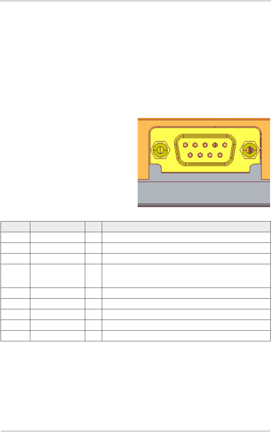
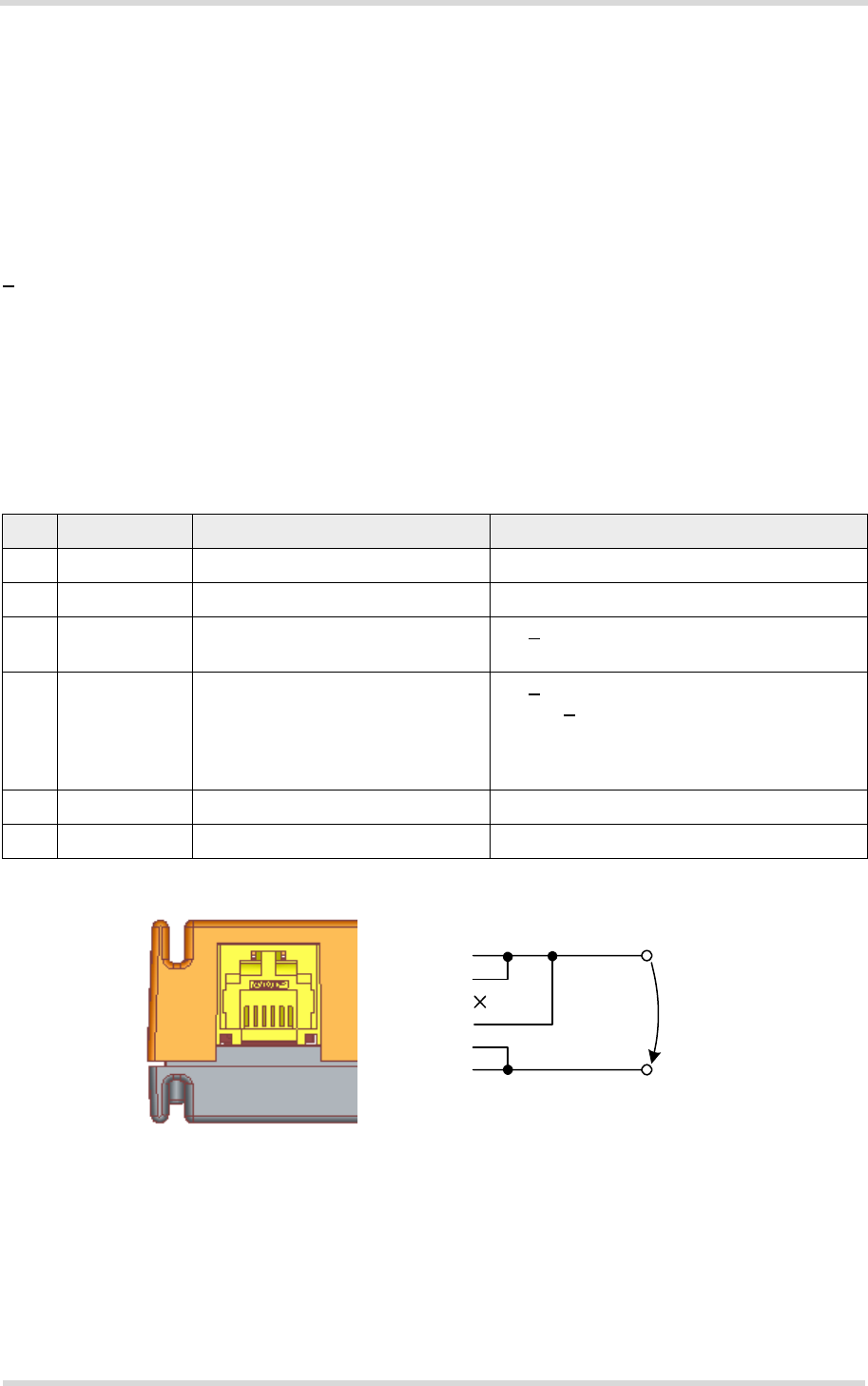
3.5.1 9-Pole D-sub Connector
Via RS-232 interface, the host controller controls the Java Terminals and transports data.
Figure 5: Pin assignment RS-232 (D-sub 9-pole female)
Java Terminals are designed for use as a DCE. Based on the conventions for DCE-DTE con-
nections it communicates with the customer application (DTE) using the following signals:
• Port TxD @ application sends data to TXD of the Java Terminals
• Port RxD @ application receives data from RXD of the Java Terminals
Hardware handshake using the RTS and CTS signals and XON/XOFF software flow control
are supported.
Table 11: 9-pole D-sub (female) RS-232
Pin no. Signal name I/O Function
1 DCD O Data Carrier Detected
2RXD OReceive Data
3 TXD I Transmit Data
4 DTR I Data Terminal Ready
Attention: The ignition of Java Terminals is activated via a rising
edge of high potential (+3 ... +15 V)
5 GND - Ground
6 DSR O Data Set Ready
7 RTS I Request To Send
8 CTS O Clear To Send
9 RING O Ring Indication
12345
6789
Cinterion® Java Terminals Hardware Interface Description
3.6 USB Interface
35
EHSxT_BGS5T_HID_v02 2014-08-05
Confidential / Preliminary
Page 25 of 70
In addition, the modem control signals DTR, DSR, DCD and RING are available. The modem
control signal RING (Ring Indication) can be used to indicate, to the cellular device application,
that a call or Unsolicited Result Code (URC) is received. There are different modes of opera-
tion, which can be set with AT commands.
Note: The DTR signal will only be polled once per second from the internal firmware of Java
Terminals.
3.6 USB Interface
The Java Terminals support a USB 2.0 High Speed (480Mbit/s) device interface that is Full
Speed (12Mbit/s) compliant.
The USB interface can be used as command and data interface and for downloading firmware.
It is only available as a slave device and not able to act as a USB host.
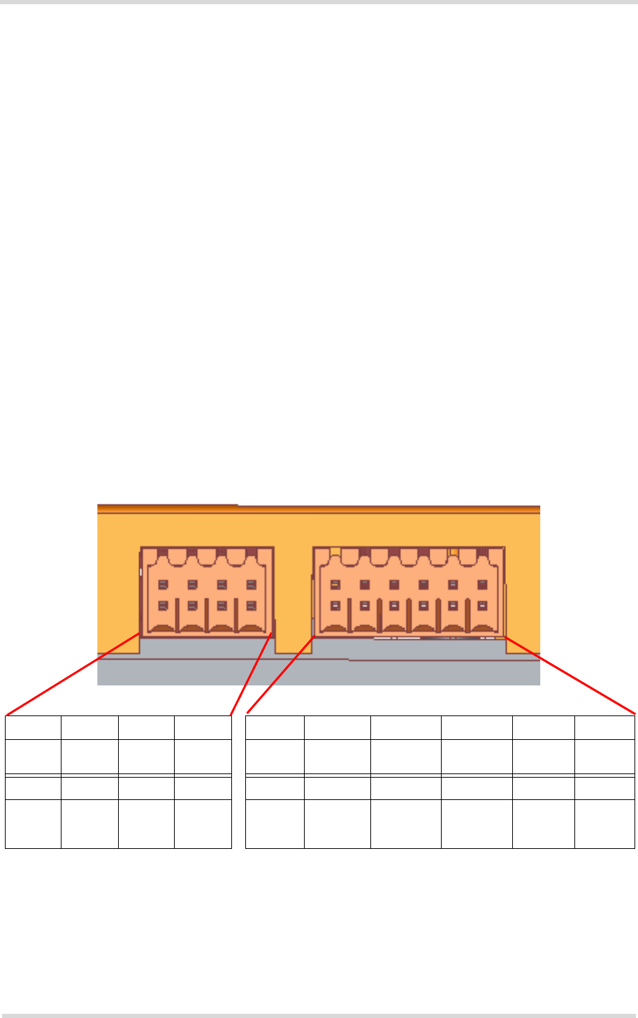
3.7 Weidmueller GPIO Interface
The Weidmueller connectors (8-pin and 12-pin) provide access to various module signals in-
cluding a number of configurable GPIOs. Note that not all of the Weidmueller pins are available
for every Java Terminal variant. The following figures show the available pins for the Java Ter-
minal variants and the below Table 12 lists the overall availablility of the Weidmueller pins.
Figure 6: EHS5T RS485: Weidmueller connectors (8-pin and 12-pin)
1234 1 2 3 4 5 6
GPIO6 GPIO7 GPIO8 n/a VCCref GND TXD1/
SPI_MISO RXD1/
SPI_MOSI A+
(RS485) B-
(RS485)
5678 7 8 9 10 1112
n/an/an/an/a +5VoutDSR0/
ADC1_IN/
SPI_CLK
I2CDAT I2CCLK GPIO20 GPIO21
EHS5T
n/a: not applicable
RS485:
Cinterion® Java Terminals Hardware Interface Description
3.7 Weidmueller GPIO Interface
35
EHSxT_BGS5T_HID_v02 2014-08-05
Confidential / Preliminary
Page 26 of 70
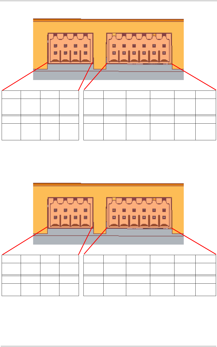
Figure 7: EHS6T USB: Weidmueller connectors (8-pin and 12-pin)
Figure 8: BGS5T USB: Weidmueller connectors (8-pin and 12-pin)
1234 1 2 3 4 5 6
GPIO6 GPIO7 GPIO8 GPIO11 VCCref GND TXD1/
SPI_MISO RXD1/
SPI_MOSI CTS1
(RS232)/
SPI_CS
RTS1
(RS232/
5678 7 8 9 10 1112
GPIO12 GPIO13 GPIO14 GPIO15 +5Vout DSR0/
ADC1_IN/
SPI_CLK
I2CDAT I2CCLK GPIO20 GPIO21
EHS6T
USB:
1234 1 2 3 4 5 6
GPIO6 GPIO7 GPIO8 n/a VCCref GND TXD1 RXD1 CTS1
(RS232)/ RTS1
(RS232/
5678 7 8 9 10 1112
n/an/an/an/a +5VoutDSR0/
ADC1_IN I2CDAT I2CCLK GPIO20 GPIO21
BGS5T
n/a: not applicable
USB:
Cinterion® Java Terminals Hardware Interface Description
3.7 Weidmueller GPIO Interface
35
EHSxT_BGS5T_HID_v02 2014-08-05
Confidential / Preliminary
Page 27 of 70
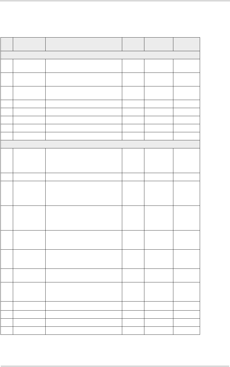
The following Table 12 shows the availablility of the Weidmueller pins for various Java Terminal
variants.
Please refer to the respective “AT Command Set“ for details on how to configure the GPIO pins.
Table 12: Weidmueller pin availability
PI
NSignal Comment EHS5T
RS485 EHS6T
USB BGS5T
USB
8-pin connector
1 GPIO6 Configurable via AT command,
also as PWM2 signal
2 GPIO7 Configurable via AT command,
also as PWM1 signal
3 GPIO8 Configurable via AT command,
also as COUNTER signal
4 GPIO11 Configurable via AT command - -
5 GPIO12 Configurable via AT command - -
6 GPIO13 Configurable via AT command - -
7 GPIO14 Configurable via AT command - -
8 GPIO15 Configurable via AT command - -
12-pin connector
1 VCCref Input supply for level converter to
specify external power level
(e.g., connect +5Vout for 5V
power level)
2GND
3TXD1 or
SPI_MISO Configurable via AT command,
also as SPI_MISO signal TXD1
or
SPI_MI
SO
TXD1 or
SPI_MISO TXD1
4 RXD1 or
SPI_MOSI Configurable via AT command,
also as SPI_MOSI signal RXD1
or
SPI_M
OSI
RXD1 or
SPI_MOSI RXD1
5CTS1 or
SPI_CS or
A+
Either CTS1 (for RS-232) or
SPI_CS or A+ (for RS-485)
depending on product variant
A+
(RS-
485)
CTS1 or
SPI_CS CTS1
6RTS1 or
B- Either RTS1 (for RS-232) or B-
(for RS-485) depending on prod-
uct variant
B-
(RS-
485
RTS1 RTS1
7 +5Vout External power supply up to
100mA, usable as VCCref input
8 DSR0 or
ADC1_IN or
SPI_CLK
Configurable via AT command
(no SPI)
9 I2CDAT I2C interface
10 I2CCLK I2C interface
11 GPIO20 Configurable via AT command
12 GPIO21 Configurable via AT command

Cinterion® Java Terminals Hardware Interface Description
3.7 Weidmueller GPIO Interface
35
EHSxT_BGS5T_HID_v02 2014-08-05
Confidential / Preliminary
Page 28 of 70
EHS5T‘s RS-485 interface is based on the TIA/EIA-485 standard defining electrical character-
istics of drivers and receivers for use in balanced multidrop communication systems. RS-485
is used in a lot of different fieldbus systems like Profibus, Interbus, Modbus and P-net.
RS-485 uses a shielded twisted pair cable where the shield is used as ground return, and the
inner pairs are used for balanced communication. The two conductors in each pair are called
A and B. RS-485 is usually half-duplex.
Data transmission speed depends on the length of the RS-485 bus cable and may be up to
115kbps.
Cinterion® Java Terminals Hardware Interface Description
3.8 Power Supply
35
EHSxT_BGS5T_HID_v02 2014-08-05
Confidential / Preliminary
Page 29 of 70
3.8 Power Supply
The power supply of the Java Terminals has to be a single voltage source of VPLUS=8V…30V
capable of providing a peak current (pulsed 2x577ms at T=4.615ms) of about 1.2A at 8V during
an active transmission. The uplink burst causes strong ripple (drop) on the power lines. The
drop voltage should not exceed 1V, but the absolute minimum voltage during drops must be
>7.6V.
The Java Terminals are protected from supply voltage reversal. An external fast acting fuse
>0.4A with melting integral I2t (0.15 … 0.25)A2s is necessary to use the Java Terminals at a
12V or 24V unlimited power supply system.
The power supply must be compliant with the EN60950 guidelines. A switching regulator reg-
ulates the input voltage for the internal supply.
When power fails for >1ms, Java Terminals reset or switch off. The watchdog can be configured
to restart the Java Terminals. When power fails for >15s the RTC will be reset.
Figure 9: 6-pole Western jack for power supply, ignition, reset, typical connection
Mains adapter: If it fits into the design of your application we recommend the plug-in supply unit
used with the type approved Gemalto M2M reference setup. Ordering information can be found
in Chapter 7. This 12V mains adapter comes with a 6-pole Western plug and provides an inter-
nal connection between IGT_IN pin and PLUS pin for auto ignition (power up).
Table 13: Female 6-pole Western plug for power supply, ignition, power down
Pin Signal name Use Parameters
1 PLUS Power supply 8V – 30V DC, max. 33V for 1 min
2 PLUS Power supply 8V – 30V DC, max. 33V for 1 min
3 RST_IN Signal for module reset UIH > 8V for t>10ms resets the terminal.
UIL <2V and low level for normal operation.
4 IGT_IN Ignition UIH >8V
Ignition >8V for more than 200ms switches
the Java Terminals on. Ignition is activated
only by a rising edge. The rise time is
<20ms
5 GND Ground 0V
6 GND Ground 0V
Pin assignmment and typical connection:
1 PLUS
2 PLUS
3 RST_IN
4 IGT_IN
5 GND
6 GND
VPLUS DC
6 5 4 3 2 1
11

Cinterion® Java Terminals Hardware Interface Description
3.8 Power Supply
35
EHSxT_BGS5T_HID_v02 2014-08-05
Confidential / Preliminary
Page 30 of 70
3.8.1 Turn Java Terminals on
Java Terminals are turned on by plugging an appropriate power supply unit between PLUS and
GND of the 6-pole Western jack.
While the RST_IN pin (pin 3) is not active (voltage <2V) you can start the Java Terminals by
activating the RS-232 DTR line if in POWER DOWN mode.
The IGT_IN signal (pin 4) may be used to switch on Java Terminals if in POWER DOWN mode.
The watchdog can also be configured to turn the Java Terminals on if in POWER DOWN mode.
After startup of the Java Terminals the RS-232 lines are in an undefined state for approx.
900ms. This may cause undefined characters to be transmitted over the RS-232 lines during
this period.
3.8.2 Reset Java Terminals
An easy way to reset the Java Terminals is entering the command AT+CFUN=x,1. For details
on AT+CFUN please see [1].
The watchdog can also be configured to reset the Java Terminals if in POWER DOWN mode.
As an alternative, you can shut down the Java Terminals as described in Section 3.8.3 and then
restart it as described in Section 3.8.1.
3.8.3 Turn Java Terminals off
Normal shutdown:
• To turn off the Java Terminals use the AT^SMSO command, rather than disconnecting the
mains adapter.
This procedure lets the Java Terminals log off from the network and allows the software to
enter a secure state and save data before disconnecting the power supply. After AT^SMSO
has been entered the Java Terminals returns the following result codes:
^SMSO: MS OFF
OK
^SHUTDOWN
The "^SHUTDOWN" result code indicates that the Java Terminals turns off in less than
1 second. After the shutdown procedure is complete the Java Terminals enters the
POWER DOWN mode. The yellow LED stops flashing (see Section 3.13 for a detailed LED
description). The RTC is still fed from the voltage regulator in the power supply ASIC.
Please note that if there is an auto ignition connection between PLUS and IGT_IN the mod-
ule will restart automatically after a normal shutdown.

Cinterion® Java Terminals Hardware Interface Description
3.8 Power Supply
35
EHSxT_BGS5T_HID_v02 2014-08-05
Confidential / Preliminary
Page 31 of 70
Emergency restart:
• In the event of software hang-ups etc. the Java Terminals can be restarted by applying a
voltage >8V to the RST_IN pin (pin 3) for more than 10ms.
The RST_IN signal restarts the Java Terminals.
Caution: Use the RST_IN pin only when, due to serious problems, the software is not
responding for more than 5 seconds. Pulling the RST_IN pin causes the loss of all informa-
tion stored in the volatile memory since power is cut off immediately. Therefore, this proce-
dure is intended only for use in case of emergency, e.g. if Java Terminals fails to shut down
properly.
Watchdog shutdown:
• The watchdog can also be configured to turn the Java Terminals off.
When the Java Terminals enter the POWER DOWN mode, e.g. after you have issued the
AT^SMSO command or activated the RST_IN signal, all RS-232 interface lines are active for
a period of 50ms to max. 3.5s. This may cause undefined characters to be transmitted on the
RS-232 lines which can be ignored.
3.8.4 Disconnecting power supply
Before disconnecting the power supply from the PLUS pin, make sure that the Java Terminals
are in a safe condition. The best way is to wait 1s after the "^SHUTDOWN" result code has
been indicated.

Cinterion® Java Terminals Hardware Interface Description
3.9 Automatic thermal shutdown
35
EHSxT_BGS5T_HID_v02 2014-08-05
Confidential / Preliminary
Page 32 of 70
3.9 Automatic thermal shutdown
An on-board NTC measures the temperature of the built-in BGS2 module. If over- or undertem-
perature is detected on the module the Java Terminals automatically shut down to avoid ther-
mal damage to the system. Table 17 specifies the ambient temperature threshold for the Java
Terminals.
The automatic shutdown procedure is equivalent to the power-down initiated with the
AT^SMSO command, i.e. Java Terminals log off from the network and the software enters a
secure state avoiding loss of data. In IDLE mode it takes typically one minute to deregister from
the network and to switch off.
Alert messages transmitted before the Java Terminals switch off are implemented as Unsolic-
ited Result codes (URCs). For details see the description of AT^SCTM command provided in
[1].
Thermal shutdown will be deferred if a critical temperature limit is exceeded, while an emer-
gency call or a call to a predefined phone number is in progress, or during a two minute guard
period after power up. See [1] for details.
The watchdog can be configured to restart the Java Terminals after a defined period.
3.10 Hardware Watchdog
The Java Terminals feature a programmable hardware watchdog that permanently monitors
the terminals‘ hardware and can be configured to react to various hardware states. The watch-
dog may for example be configured to periodically restart the terminal, independant of its cur-
rent operating state. Figure 4 shows how the watchdog is integrated into the Java Terminals.
Please refer to Chapter 8 for details on how to control and configure the hardware watchdog.
3.11 RTC
The internal Real Time Clock (RTC) of the Java Terminals retains the time and date and han-
dles the alarm (reminder) function. The AT+CCLK command serves to set the time and date,
and AT+CALA specifies a reminder message. See [1] for details.
A dedicated voltage regulator backs up the RTC even in Power Down mode and enables Java
Terminals to keep track of time and date.
However, please note that the Alarm mode described in [1], Section AT+CALA, is not intended
for the Java Terminals. The AT+CALA command can only be used to set a reminder message,
but not to configure the mobile to wake up from POWER DOWN mode into Alarm mode. There-
fore, after setting a timer with AT+CALA be sure not to shut down the Java Terminals by
AT^SMSO or RST_IN signal.
Cinterion® Java Terminals Hardware Interface Description
3.12 SIM Interface
35
EHSxT_BGS5T_HID_v02 2014-08-05
Confidential / Preliminary
Page 33 of 70
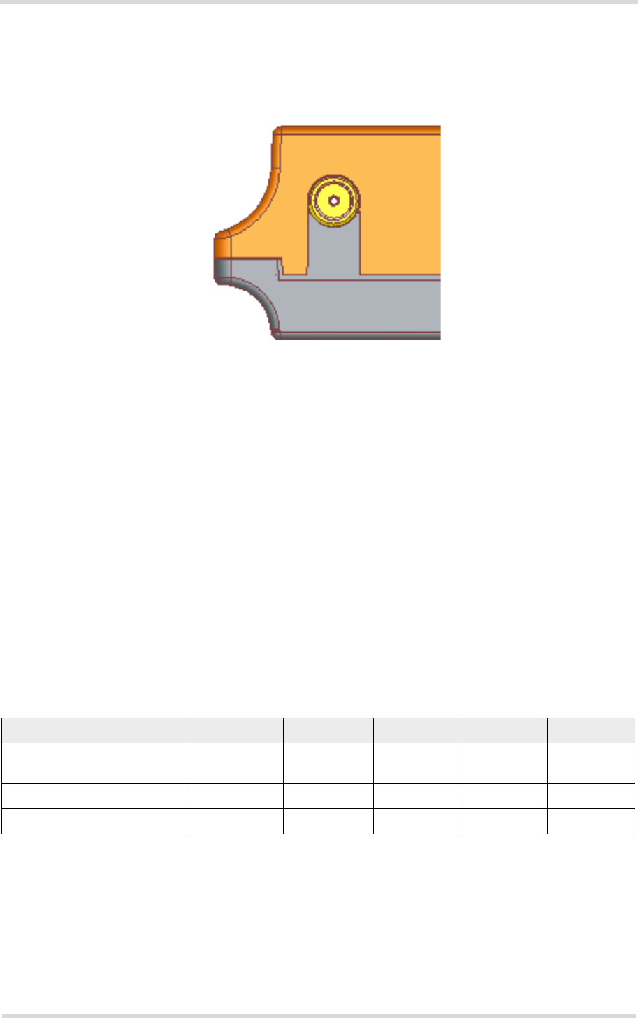
3.12 SIM Interface
The SIM interface is intended for 1.8V and 3V SIM cards in accordance with GSM 11.12 Phase
2. The card holder is a five wire interface according to GSM 11.11. A sixth pin has been added
to detect whether or not a SIM card is inserted.
Figure 10: SIM interface
The SIM - with the circuit side facing upwards - is inserted by gently pushing it into the SIM card
holder until it snaps hold. It is now protected from accidental removal. The SIM can be removed
from the card holder by using a flat object such as a screwdriver to carefully press the inserted
SIM until it snaps out again.
All signals of the SIM interface are protected from electrostatic discharge with spark gaps to
GND and clamp diodes to 1.8V resp. 2.9V and GND.
Removing and inserting the SIM card during operation requires the software to be reinitialized.
Therefore, after reinserting the SIM card it is necessary to restart Java Terminals.
Note: No guarantee can be given, nor any liability accepted, if loss of data is encountered after
removing the SIM card during operation. Also, no guarantee can be given for properly initializ-
ing any SIM card that the user inserts after having removed a SIM card during operation. In this
case, the application must restart the Java Terminals.
SIM inserted
Cinterion® Java Terminals Hardware Interface Description
3.13 Status LEDs
35
EHSxT_BGS5T_HID_v02 2014-08-05
Confidential / Preliminary
Page 34 of 70
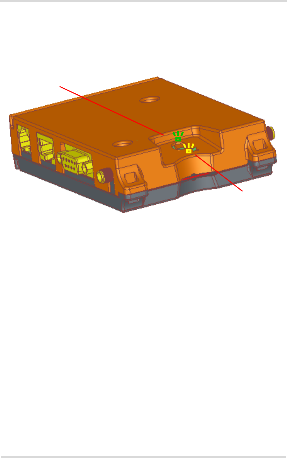
3.13 Status LEDs
Java Terminals have two LEDs indicating its operating states through the semitransparent cas-
ing:
• A green LED indicates whether the Java Terminals are ready to operate.
• A yellow LED indicates the network registration state of the Java Terminals.
Figure 11: Status LED
The yellow LED is driven by a line of the integrated module that can be configured by using the
AT^SLED command to either light permanently or to flash. For details on the AT command
please refer to [1].
Green LED
(Power on/off)
Yellow LED
(Network status)
Cinterion® Java Terminals Hardware Interface Description
3.14 RF Antenna Interface
35
EHSxT_BGS5T_HID_v02 2014-08-05
Confidential / Preliminary
Page 35 of 70
3.14 RF Antenna Interface
An external RF antenna is connected via the Java Terminals’s female SMA connector that is
also the antenna reference point (ARP).
Figure 12: Antenna connector
The system impedance is 50. In any case, for good RF performance, the return loss of the
customer application’s antenna should be better than 10dB (VSWR < 2). Java Terminals with-
stand a total mismatch at this connector when transmitting with power control level for maxi-
mum RF power.
Inside the Java module an inductor to ground provides additional ESD protection to the anten-
na connector. To protect the inductor from damage no DC voltage must be applied to the an-
tenna circuit.
For the application it is recommended to use an antenna with an SMA (male) connector:
Please note that the terminal should be installed and operated with a minimum distance of
20cm between the antenna connected to the terminal and any human bodies. Also, the trans-
mitter must not be co-located or operating in conjunction with any other antenna or transmitter.
The allowed maximum antenna gain (including cable loss) for stand-alone situation is given be-
low in Table 14.
Table 14: Allowed maximum antenna gain (including cable loss)
Module 850MHz 900MHz 1800MHz 1900MHz 2100MHz
EHS6T USB 3.42dBi 4.18dBi 9.64dBi 2.51dBi 15.54dBi
BGS5T USB 2.15dBi 2.15dBi 2.15dBi 2.15dBi na
EHS5T RS485 na 6.10dBi 12.30dBi na 12.30dBi
Cinterion® Java Terminals Hardware Interface Description
4 Electrical and Environmental Characteristics
44
EHSxT_BGS5T_HID_v02 2014-08-05
Confidential / Preliminary
Page 36 of 70
4 Electrical and Environmental Characteristics
4.1 Absolute Maximum Ratings
Table 15: Absolute maximum ratings
Parameter Port / Description Min. Max. Unit
Supply voltage PLUS -40 30 V
Overvoltage PLUS / for 1min 33 V
Input voltage for on/off
control lines IGT_IN, RST_IN -5 30 V
RS-232 input voltage TXD, DTR, RTS -25 +25 V
Weidmueller pins input volt-
age (incl. VCCref) 8-pin and 12-pin connectors
(if pins specified/configured as input pins) -0.3 6 V
Weidmueller pins output
current 8-pin and 12-pin connectors
(if pins specified/configured as output pins) 0 50mA drawn
@each pin1
1. Please note that if the VCCref pin is connected to the +5Vout pin, no more than 100mA should be drawn
by all pins. In this case it is no longer allowed to draw a maximum of 50mA for each pin.
--
USB interface All electrical characteristics according to
USB Implementers' Forum, USB 2.0 Spec-
ification.
-- -- --
Immunity against discharge
of static electricity All interfaces (lines)
Contact discharge
Human body model -8
-15 +8
+15 kV
kV
Table 16: Operating supply voltage for Java Terminals
Parameter Min Typ Max Unit
Supply voltage PLUS
measured at (6-pole)
western jack plug (1 to 6)
@any time, incl. all ripple
and drops
5.5 12 30 V

Cinterion® Java Terminals Hardware Interface Description
4.2 Operating Temperatures
44
EHSxT_BGS5T_HID_v02 2014-08-05
Confidential / Preliminary
Page 37 of 70
4.2 Operating Temperatures
Note: Within the specified operating temperature ranges the board temperature may vary to a
great extent depending on operating mode, used frequency band, radio output power and cur-
rent supply voltage. Note also the differences and dependencies that usually exist between
board (PCB) temperature of the Java module and its ambient temperature.
Table 17: Board temperature of Java module
Parameter Min Max Unit
Normal operation -30 +85 °C
Extended operation1
1. Extended operation allows normal mode speech calls or data transmission for limited time until automatic
thermal shutdown takes effect. Within the extended temperature range (outside the normal operating
temperature range) the specified electrical characteristics may be in- or decreased.
-40 to -30 +85 to +90 °C
Automatic thermal shutdown2
2. Due to temperature measurement uncertainty, a tolerance of ±3°C on these switching thresholds may
occur.
<-40 >+90 °C

Cinterion® Java Terminals Hardware Interface Description
4.3 Storage Conditions
44
EHSxT_BGS5T_HID_v02 2014-08-05
Confidential / Preliminary
Page 38 of 70
4.3 Storage Conditions
The conditions stated above are only valid for devices in their original packed state in weather
protected, non-temperature-controlled storage locations. Normal storage time under these
conditions is 12 months maximum.
Table 18: Storage conditions
Type Condition Unit Reference
Air temperature: Low
High -30
+75 °C ETS 300 019-2-1: T1.2, IEC 60068-2-1 Ab
ETS 300 019-2-1: T1.2, IEC 60068-2-2 Bb
Humidity relative: Low
High
Condens.
10
90 at 30°C
90-100 at 30°C
%---
ETS 300 019-2-1: T1.2, IEC 60068-2-56
Cb
ETS 300 019-2-1: T1.2, IEC 60068-2-30
Db
Air pressure: Low
High 70
106 kPa IEC TR 60271-3-1: 1K4
IEC TR 60271-3-1: 1K4
Movement of surrounding air 1.0 m/s IEC TR 60271-3-1: 1K4
Water: rain, dripping, icing and
frosting Not allowed --- ---
Radiation: Solar
Heat 1120
600 W/m2ETS 300 019-2-1: T1.2, IEC 60068-2-2 Bb
ETS 300 019-2-1: T1.2, IEC 60068-2-2 Bb
Chemically active substances Not
recommended IEC TR 60271-3-1: 1C1L
Mechanically active substances Not
recommended IEC TR 60271-3-1: 1S1
Vibration sinusoidal:
Displacement
Acceleration
Frequency range
1.5
5
2-9 9-200
mm
m/s2
Hz
IEC TR 60271-3-1: 1M2
Shocks:
Shock spectrum
Duration
Acceleration
semi-sinusoidal
1
50 ms
m/s2
IEC 60068-2-27 Ea
Cinterion® Java Terminals Hardware Interface Description
4.4 Electrical Specifications of the Application Interface
44
EHSxT_BGS5T_HID_v02 2014-08-05
Confidential / Preliminary
Page 39 of 70
4.4 Electrical Specifications of the Application Interface
4.4.1 On/Off Control
4.4.2 RS-232 Interface
4.4.3 USB Interface
All electrical characteristics according to USB Implementers' Forum, USB 2.0 Specification.
Table 19: On/Off control line specifications
Parameter Description Conditions Min. Typ Max. Unit
Vhigh Input voltage
IGT_IN, RST_IN active high 4 28 V
Vlow 03V
Vhigh Input voltage
DTR active high 3 +15 V
Vlow -15 1.2 V
RIN Input resistance of
IGT_IN, RST_IN 1M
RIN Input resistance of
DTR 357k
Table 20: RS-232 interface specifications
Parameter Description Conditions Min. Typ Max. Unit
VOUT Transmitter output voltage
for
RXD, CTS, DSR, DCD,
RING
@ 3k load ±5 ±6 ±7 V
ROUT Transmitter output resis-
tance
RXD, CTS, DSR, DCD,
RING
300
RIN Resistance
TXD, RTS, DTR 357k
VIn Receiver input voltage
range
TXD, RTS, DTR
-25 +25 V
VRIHYS Input hysteresis 0.5 V
VIlow Input threshold low 0.6 1.2 V
VIhigh Input threshold high 1.5 2.4 V
Baudrate Autobauding 1.2 230 kbps
Fixed range 1.2 230 kbps
LECable Length of RS-232 cable 1.8 2 m
Cinterion® Java Terminals Hardware Interface Description
4.4 Electrical Specifications of the Application Interface
44
EHSxT_BGS5T_HID_v02 2014-08-05
Confidential / Preliminary
Page 40 of 70
4.4.4 Weidmueller GPIO Interface
Table 21: Weidmueller GPIO interface specifications (requirements)
Function Signal name IO Signal form and level Comment
8-pin, 12-
pin connec-
tors for:
GPIO,
Power,
I2C and
ASC1, SPI,
RS-485
GPIO 6-8
GPIO 11-15
GPIO 20-21
IO VOLmax = 0.1V at I = 100µA
VOLmax = 0.55V at I = 32mA
VOHmin = VCCref - 0.1V at I = 100µA
VOHmin = VCCref - 0.4V at I < 12mA
VOHmin = VCCref - 0.7V at I < 32mA
VILmax = 0.3 * VCCref
VIHmin = 0.7 * VCCref
If unused keep lines
open.
Please note that some
GPIO lines are or can be
configured for functions
other than GPIO:
GPIO6/GPIO7: PWM
GPIO8: Pulse Counter
VCCref I Vimax = 5.5V
Vimin = 1.8V
GND -- --
TXD1/
SPI_MISO IV
OLmax = 0.1V at I = 100µA
VOLmax = 0.55V at I = 32mA
VOHmin = VCCref - 0.1V at I = 100µA
VOHmin = VCCref - 0.4V at I < 12mA
VOHmin = VCCref - 0.7V at I < 32mA
VILmax = 0.3 * VCCref
VIHmin = 0.7 * VCCref
If unused keep lines
open.
SPI interface is not avail-
able for BGS5.
RXD1/
SPI_MOSI O
CTS1/A+/
SPI_CS O
RTS1/B- I
+5Vout O 5V, +0.05V, -0.2V
Ioutmax = 100mA Regulated output for
external supply. Can be
connected to VCCref.
If unused, keep open.
DSR0/
ADC1_IN
(Analog-to-
Digital con-
verter)/
SPI_CLK
IR
I = 1M
VImax = 0V...VCCref + 0.3V
Valid range 0V…5V
Resolution 1024 steps
Tolerance 0.3%
ADC1_IN can be used as
input for external mea-
surements.
If unused keep line open.
I2CDAT IO Open drain IO
VOLmin = 0.3V at I = -3mA
VOHmax = VCCref
Rpullup = 2.2kOhm
VILmax = 0.35V
VIHmin = 1.3V
VIHmax = 1.85V
According to the I2C Bus
Specification Version 2.1
for the fast mode a rise
time of max. 300ns is per-
mitted. There is also a
maximum VOL=0.4V at
3mA specified.
The value of the pull-up
depends on the capactive
load of the whole system
(I2C Slave + lines). The
maximum sink current of
I2CDAT and I2CCLK is
4mA.
If unused keep lines
open.
I2CCLK IO
Cinterion® Java Terminals Hardware Interface Description
4.5 Power Supply Ratings
44
EHSxT_BGS5T_HID_v02 2014-08-05
Confidential / Preliminary
Page 41 of 70
4.5 Power Supply Ratings
Table 22: Power supply specifications
Para-
meter Description Conditions Typical Unit
EHS5T
RS485 EHS6T
USB BGS5T
USB
VPLUS Allowed voltage ripple
(peak-peak), drop during
transmit burst peak current
Power control level for Pout
max1111V
IPLUS 2Average supply current
(average time 3 min.) Power Down
mode @8V 12.4 20.7 33.5 mA
@30V 6.5 9.8 13.7
Average GSM supply cur-
rent
(average time 3 min.)3
IDLE mode
(GSM/GPRS,
850/900MHz,
1800/1900MHz)
@8V 27 39.6 29.5 mA
@30V 10.4 15.9 12.7
GPRS DATA
mode(1 Tx, 4 Rx,
850/900MHz)
@8V 169.3 175 160 mA
@30V 47.2 50.3 46.2
GPRS DATA
mode(1 Tx, 4 Rx,
1800/1900MHz)
@8V 63.9 136.4 117.3 mA
@30V 21.2 38 36.1
GPRS DATA
mode(4 Tx, 1 Rx,
850/900MHz)
@8V 234.6 245 286.3 mA
@30V 67 100 81
GPRS DATA
mode(4 Tx, 1 Rx,
1800/1900MHz)
@8V 109.5 186 208.8 mA
@30V 34.1 56 61.8
EDGE DATA
mode(1 Tx, 4 Rx,
850/900MHz)
@8V 170.1 175 160 mA
@30V 47.4 50.2 46.2
EDGE DATA
mode(1 Tx, 4 Rx,
1800/1900MHz)
@8V 64.4 130.7 117.4 mA
@30V 21.3 39.7 36.2
EDGE DATA
mode(4 Tx, 1 Rx,
850/900MHz)
@8V 234.4 237.6 284.9 mA
@30V 67 69.6 81
EDGE DATA
mode(4 Tx, 1 Rx,
1800/1900MHz)
@8V 109.5 186.7 208.9 mA
@30V 34.2 56.4 62
Peak supply current (during
577µs transmission slot
every 4.6ms)
Power control
level for Pout max
(850/900MHz)
@8V 1100 1130 1200 mA
@30V 260 270 260
Power control
level for Pout max
(1800/1900MHz)
@8V 815 820 630 mA
@30V 195 200 160
Cinterion® Java Terminals Hardware Interface Description
4.5 Power Supply Ratings
44
EHSxT_BGS5T_HID_v02 2014-08-05
Confidential / Preliminary
Page 42 of 70
IPLUS Average UMTS supply cur-
rent (average time 3 min.) IDLE mode @8V 27 79 --- mA
@30V 10.7 12.3 ---
UMTS DATA
(Band I; 23dBm) @8V 313 411 --- mA
@30V 88.3 113.9 ---
UMTS DATA
Band II; 23dBm @8V --- 447.6 --- mA
@30V --- 123.8 ---
UMTS DATA
Band V/VI; 23dBm @8V --- 413.9 --- mA
@30V --- 115 ---
UMTS DATA
Band VIII; 23dBm @8V 367 410.1 --- mA
@30V 103 114.2 ---
HSPA DATA
(Band I; 23dBm) @8V 313 411 --- mA
@30V 88.3 113.9 ---
HSPA DATA
Band II; 23dBm @8V --- 447.6 --- mA
@30V --- 123.8 ---
HSPA DATA
Band V/VI; 23dBm @8V --- 413.9 --- mA
@30V --- 115 ---
HSPA DATA
Band VIII; 23dBm @8V 367 410.1 --- mA
@30V 103 114.2 ---
1. Lowest voltage (minimum peak) incl. all ripple and drops >7.6V including voltage drop, ripple and spikes,
measured at western jack (6-pole) pins.
2. Typical values measured with antenna impedance = 50 Ohm (return loss >20dB).
3. BGS5T USB does not support EDGE.
Table 22: Power supply specifications
Para-
meter Description Conditions Typical Unit
EHS5T
RS485 EHS6T
USB BGS5T
USB
Cinterion® Java Terminals Hardware Interface Description
4.6 Antenna Interface
44
EHSxT_BGS5T_HID_v02 2014-08-05
Confidential / Preliminary
Page 43 of 70
4.6 Antenna Interface
Table 23 lists RF antenna interface specifications for the Java Terminals. Please note that the
specified conditions may not apply to or be supported by all terminals.
Table 23: RF Antenna interface GSM / UMTS
Parameter Conditions Min. Typical Max. Unit
UMTS/HSPA connectivity Band I, II, V, VI, VIII (not every module variant supports all bands)
Receiver Input Sensitivity @
ARP UMTS 800/850 Band VI/V -104.7/
-106.7 -110 dBm
UMTS 900 Band VIII -103.7 -110 dBm
UMTS 1900 Band II -104.7 -109 dBm
UMTS 2100 Band I -106.7 -110 dBm
RF Power @ ARP with
50Ohm Load
Board temperature <85°C
UMTS 800/850 Band VI/V +21 +24 +25 dBm
UMTS 900 Band VIII +21 +24 +25 dBm
UMTS 1900 Band II +21 +24 +25 dBm
UMTS 2100 Band I +21 +24 +25 dBm
GPRS coding schemes Class 12, CS1 to CS4
EGPRS Class 12, MCS1 to MCS9
GSM Class Small MS
Static Receiver input Sensi-
tivity @ ARP GSM 850 / E-GSM 900 -102 -109 dBm
GSM 1800 / GSM 1900 -102 -108 dBm
RF Power @
ARP
with 50Ohm
Load
GSM GSM 850 / E-GSM 900 33 dBm
GSM 1800 / GSM 1900 30 dBm
Cinterion® Java Terminals Hardware Interface Description
4.6 Antenna Interface
44
EHSxT_BGS5T_HID_v02 2014-08-05
Confidential / Preliminary
Page 44 of 70
RF Power @
ARP
with 50Ohm
Load,
(with maxi-
mum reduc-
tion)
BGS5T USB
does not
support
EDGE, devi-
ating values
are given in
brackets
GPRS, 1 TX GSM 850 / E-GSM 900 33 dBm
GSM 1800 / GSM 1900 30 dBm
EDGE, 1 TX GSM 850 / E-GSM 900 27 dBm
GSM 1800 / GSM 1900 26 dBm
GPRS, 2 TX GSM 850 / E-GSM 900 30 dBm
GSM 1800 / GSM 1900 27
(28.3) dBm
EDGE, 2 TX GSM 850 / E-GSM 900 24 dBm
GSM 1800 / GSM 1900 23 dBm
GPRS, 3 TX GSM 850 / E-GSM 900 28.2
(27.7) dBm
GSM 1800 / GSM 1900 25.2
(27.4) dBm
EDGE, 3 TX GSM 850 / E-GSM 900 22.2 dBm
GSM 1800 / GSM 1900 21.2 dBm
GPRS, 4 TX GSM 850 / E-GSM 900 27
(25.4) dBm
GSM 1800 / GSM 1900 24
(25.2) dBm
EDGE, 4 TX GSM 850 / E-GSM 900 21 dBm
GSM 1800 / GSM 1900 20 dBm
Table 23: RF Antenna interface GSM / UMTS
Parameter Conditions Min. Typical Max. Unit
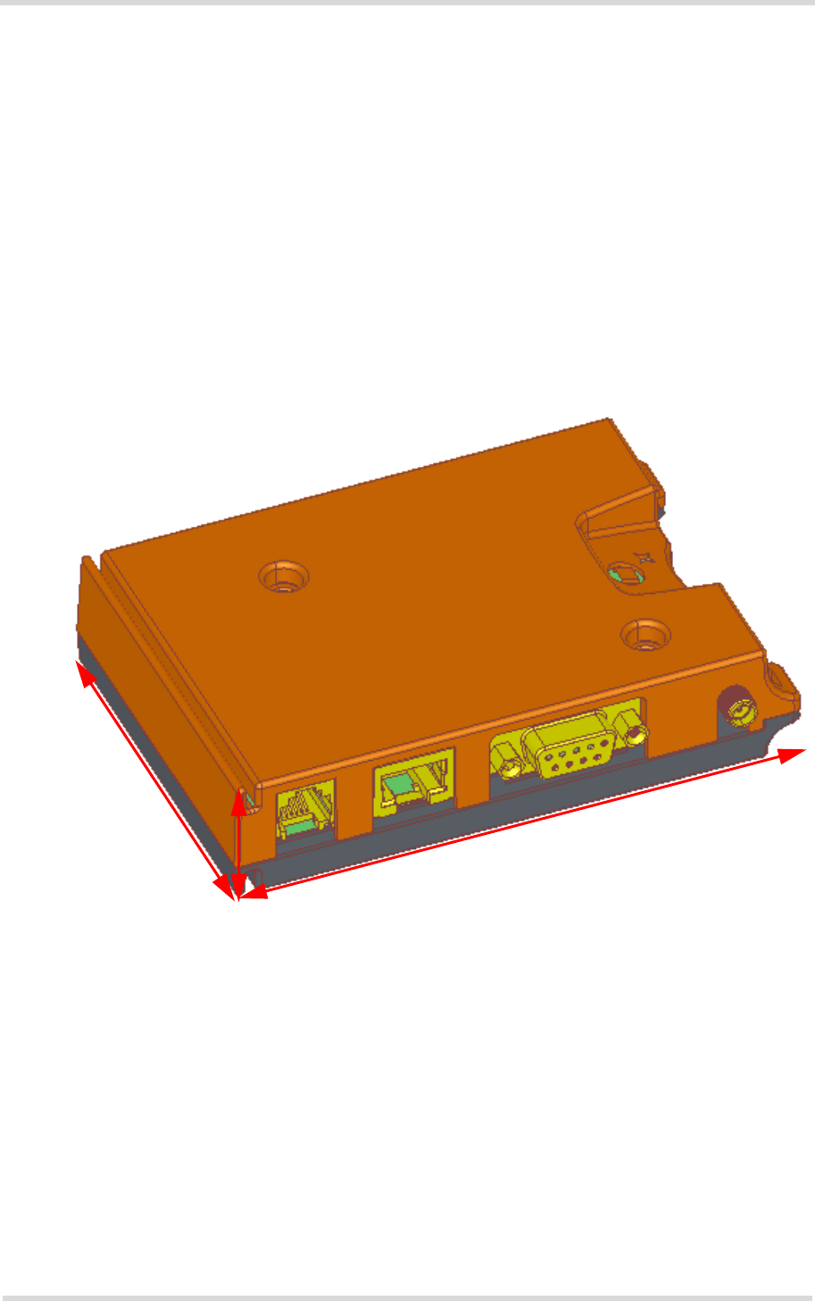
Cinterion® Java Terminals Hardware Interface Description
5 Mechanics, Mounting and Packaging
48
EHSxT_BGS5T_HID_v02 2014-08-05
Confidential / Preliminary
Page 45 of 70
5 Mechanics, Mounting and Packaging
5.1 Mechanical Dimensions
Figure 13 shows a 3D view of the Java Terminal and provides an overview of the mechanical
dimensions of the board. For further details see Figure 14. To allow for an easier mechanical
implementation into an external application a set of 3D STP data for the Java Terminals is at-
tached to this PDF. Please open the Attachments navigation panel to view and save these files.
Figure 13: Java Terminals 3D overview
Length: 113.5mm (including fixtures for cable straps)
Width: 75mm (excluding antenna and serial interface connectors)
Height: 25.5mm
Weight: 120g
113.5mm
75mm
25.5mm
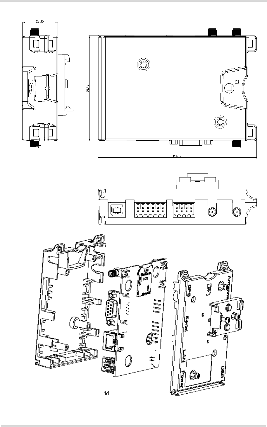
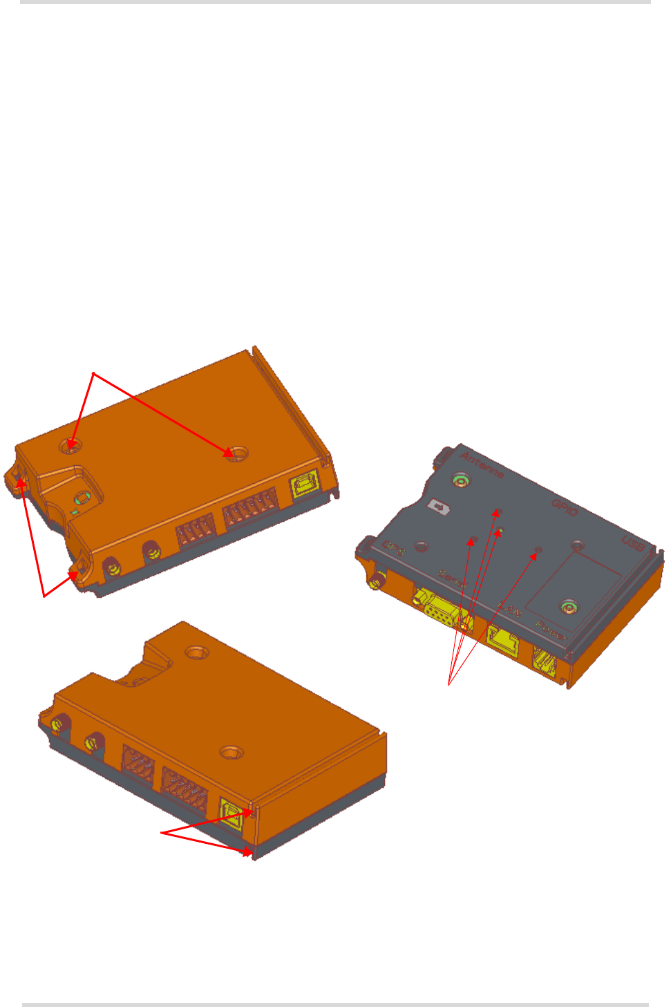
Cinterion® Java Terminals Hardware Interface Description
5.2 Mounting the Java Terminals
48
EHSxT_BGS5T_HID_v02 2014-08-05
Confidential / Preliminary
Page 47 of 70
5.2 Mounting the Java Terminals
There are a number of ways to mount the Java Terminals:
• Java Terminals can be attached to a rail installation or other surface using the two provided
screw holes.
• Java Terminals can be fastened to a rack or holding using the two provided fixtures for
cable straps.
• Java Terminals can be slid onto a specific DIN rail made according to DIN EN 60715 - C
section, C30 format. A catch at the terminal’s bottom side will have to be removed to slide
multiple terminals onto a single rail.
• Using a BOPLA TSH 35-2 universal DIN rail holder the Java Terminals can be fitted onto
another special type of DIN rail made according to DIN EN 60715 - Top hat section, 35mm
(e.g., Wago 210-113 steel carrier rail).
The following figure shows the various possibilities provided to mount the Java Terminals.
Figure 15: Mounting the Java Terminals
The various ways to mount the Java Terminals may be combined where appropriate. It is for
example possible to slide the terminal onto a DIN rail and in addition use cable straps to fasten
it to a holding.
Catch to mount
Screw holes for
Screw holes
Fixtures for
cable straps
DIN rail holder
C-rail (C30)
BOPLA TSH 35-2

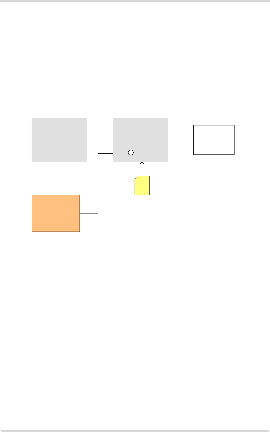
Cinterion® Java Terminals Hardware Interface Description
6 Full Type Approval
52
EHSxT_BGS5T_HID_v02 2014-08-05
Confidential / Preliminary
Page 49 of 70
6 Full Type Approval
6.1 Gemalto M2M Reference Setup
The Gemalto M2M reference setup submitted to type approve Java Terminals consists of the
following components:
• Java Terminals with approved Java module
•PC as MMI
• Power Supply
Figure 16: Reference equipment for approval
For ordering information please refer to Chapter 7.
PC
Power supply
SIM
RS-232/
USB Java
Terminal
Antenna
or
50Ohm cable
to the
system simulator
ARP
Cinterion® Java Terminals Hardware Interface Description
6.2 Restrictions
52
EHSxT_BGS5T_HID_v02 2014-08-05
Confidential / Preliminary
Page 50 of 70
6.2 Restrictions
Later enhancements and modifications beyond the certified configuration require extra approv-
als. Each supplementary approval process includes submittal of the technical documentation
as well as testing of the changes made.
• No further approvals are required for customer applications that comply with the approved
Java Terminals configuration.
• Extra approval must be obtained for applications using other accessories than those
included in the approved Java Terminals configuration (power supply, MMI implementation
supported by AT commands).
6.3 CE Conformity
The Java Terminals meet the requirements of the EU directives listed below:
• R&TTE Directive 1999/5/EC
The Java Terminals are marked with the CE conformity mark (including notified body number):
6.4 EMC
The Java Terminals comply with the equipment requirements specified in EN 301489-1, -7 and
-24 are covered by the R&TTE Directive.
EHSxT BGS5T USB

Cinterion® Java Terminals Hardware Interface Description
6.5 Compliance with FCC and IC Rules and Regulations
52
EHSxT_BGS5T_HID_v02 2014-08-05
Confidential / Preliminary
Page 51 of 70
6.5 Compliance with FCC and IC Rules and Regulations
As an integrated product, the Java Terminals EHS6T USB and BGS5T RS485 are fully com-
pliant with the grant of the FCC Equipment Authorization and the Industry Canada Certificates
issued for the built-in Java modules, and therefore, bear the labels “Contains FCC ID
QIPEHS6” or “Contains FCC ID QIPBGS5.
The Equipment Authorization Certification for the Cinterion® Java modules is listed under the
following identifiers:
FCC Idenitifier: QIPEHS6 or QIPBGS5
Industry Canada Certification Number: 7830A-EHS6 or 7830A-BGS5
Granted to Gemalto M2M GmbH
Notes (FCC):
Radiofrequency radiation exposure Information:
This equipment complies with FCC radiation exposure limits set forth for an uncontrolled envi-
ronment. This equipment should be installed and operated with minimum distance of 20 cm be-
tween the radiator and your body. This transmitter must not be co-located or operating in
conjunction with any other antenna or transmitter.
This device complies with part 15 of the FCC Rules. Operation is subject to the following two
conditions: (1) This device may not cause harmful interference, and (2) this device must accept
any interference received, including interference that may cause undesired operation.
This terminal equipment has been tested and found to comply with the limits for a Class B dig-
ital device, pursuant to Part 15 of the FCC Rules. These limits are designed to provide reason-
able protection against harmful interference in a residential installation. This equipment
generates, uses and can radiate radio frequency energy and, if not installed and used in accor-
dance with the instructions, may cause harmful interference to radio communications. Howev-
er, there is no guarantee that interference will not occur in a particular installation. If this
equipment does cause harmful interference to radio or television reception, which can be de-
termined by turning the equipment off and on, the user is encouraged to try to correct the inter-
ference by one or more of the following measures:
• Reorient or relocate the receiving antenna.
• Increase the separation between the equipment and receiver.
• Connect the equipment into an outlet on a circuit different from that to which the receiver is
connected.
• Consult the dealer or an experienced radio/TV technician for help.
Changes or modifications made to this equipment not expressly approved by Gemalto M2M
may void the FCC authorization to operate this equipment.
This device contains UMTS, GSM and GPRS class functions in the 900, 1800 and 2100MHz
bands that are not operational in U.S. Territories. This device is to be used only for mobile and
fixed applications.
Users and installers must be provided with antenna installation instructions and transmitter op-
erating conditions for satisfying RF exposure compliance: For more information on the RF an-
tenna interface please refer to Section 3.14 and Section 4.6.

Cinterion® Java Terminals Hardware Interface Description
6.5 Compliance with FCC and IC Rules and Regulations
52
EHSxT_BGS5T_HID_v02 2014-08-05
Confidential / Preliminary
Page 52 of 70
Notes (IC):
(EN) This Class B digital apparatus complies with Canadian ICES-003 and RSS-210. Opera-
tion is subject to the following two conditions: (1) this devive may not cause interference, and
(2) this device must accept any interference, including interference that may cause undesired
operation of the device.
(FR) Cet appareil numérique de classe B est conforme aux normes canadiennes ICES-003 et
RSS-210. Son fonctionnement est soumis aux deux conditions suivantes: (1) cet appareil ne
doit pas causer d'interférence et (2) cet appareil doit accepter toute interférence, notamment
les interférences qui peuvent affecter son fonctionnement.
(EN) Radio frequency (RF) Exposure Information
The radiated output power of the Wireless Device is below the Industry Canada (IC) radio fre-
quency exposure limits. The Wireless Device should be used in such a manner such that the
potential for human contact during normal operation is minimized.
This device has also been evaluated and shown compliant with the IC RF Exposure limits un-
der mobile exposure conditions. (antennas are greater than 20cm from a person‘s body).
(FR) Informations concernant l'exposltion aux fréquences radio (RF)
La puissance de sortie émise par l'appareil de sans fiI est inférieure à la limite d'exposition aux
fréquences radio d‘Industry Canada (IC). Utilisez l'appareil de sans fil de façon à minimiser les
contacts humains lors du fonctionnement normal.
Ce périphérique a également été évalué et démontré conforme aux limites d'exposition aux RF
d'IC dans des conditions d'exposition à des appareils mobiles (les antennes se situent à moins
de 20cm du corps d'une personne).
Cinterion® Java Terminals Hardware Interface Description
7 List of Parts and Accessories
53
EHSxT_BGS5T_HID_v02 2014-08-05
Confidential / Preliminary
Page 53 of 70
7 List of Parts and Accessories
Table 24: List of parts and accessories
Description Supplier Ordering information
Java Terminals Gemalto M2M Ordering number
EHS5T RS485: L30960-N2730-A100
EHS6T USB: L30960-N2740-A100
BGS5T USB: L30960-N2720-A100
Power supply unit Gemalto M2M Terminal Power Supply (incl. EU adapter)
Ordering number: L36880-N8490-A12
UK adapter for above Terminal Power Supply
Ordering number: L36880-N8490-A13
US adapter for above Terminal Power Supply
Ordering number: L36880-N8490-A14
AU adapter for above Terminal Power Supply
Ordering number: L36880-N8490-A15
DIN rail holder - BOPLA TSH 35-2 BOPLA Ordering number: 20035000
BOPLA Gehäuse Systeme GmbH
Borsigstr. 17-25
D-32257 Bünde
Phone: +49 (0)5223 / 969 - 0
Fax: +49 (0)5223 / 969 - 100
Email: iinfo@bopla.de
Web: http://www.bopla.de
Antenna - SMARTEQ-MiniMAG
Dualband, 0dBd, 2.6m RG174,
SMA (m)
KÖBEL Mobile
Communication Ordering number: 1140.26 with crimped SMA
connector
KÖBEL Mobile Communication
Sesamstrasse 12
D-24632 Lentföhrden
RS-232 cable with 9-pin D-sub
connector (male) Tecline Ordering number: 300574
Tecline GmbH
Behrener Straße 8
D-66117 Saarbrücken
Phone: +49-681-926-78-70
Fax: +49-681-926-78-555
Web: http://www.tecline-edv.de/
8-pin and 12-pin header connec-
tor (male) for Weidmueller GPIO
interface
Weidmueller Ordering number (12-pin): 1277510000
Ordering number (8-pin): 1277480000
Weidmüller Interface GmbH & Co. KG
Klingenbergstraße 16
D-32758 Detmold
Phone: +49 5231 14-0
Fax: +49 5231 14-2083
Email: iinfo@weidmueller.de
Web: http://www.weidmueller.com
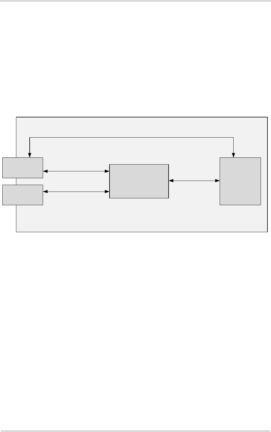
Cinterion® Java Terminals Hardware Interface Description
8 Appendix A: (Hardware) Watchdog
69
EHSxT_BGS5T_HID_v02 2014-08-05
Confidential / Preliminary
Page 54 of 70
8 Appendix A: (Hardware) Watchdog
The watchdog is part of the Java Terminals and connected to the Java module itself (see also
Figure 4). It can be used to
• Safely reset the module in certain conditions
• Restart the module when it has turned off
• Configure GPIOs and DSR0/ADC1_IN available at the Weidmueller connector
The complete watchdog functionality can be configured via the serial interface ASC0 (for de-
tails see Section 8.3). Some configuration commands can also be specified via I2C interface
(for details see Section 8.4). Figure 17 shows how the watchdog may be accessed.
Figure 17: Hardware watchdog
8.1 Reset Conditions
The watchdog implements three conditions, under which a reset of the module is automatically
performed:
• Repetitive: A module reset is performed frequently and repetitive. This reset condition can
be used to force the module to reconnect to the mobile network once in a while. Typical fre-
quencies are 24 hours or more. This feature can be configured via the RST_REP timeout.
• UART activity: The watchdog can be used to reset the module, when no activity from the
module on the UART interface is recognized for a specified amount of time. To prevent the
reset, the module has to be active frequently on the UART interface. This reset condition
can be configured via the RST_UART timeout, it is deactivated when timeout parameter = 0.
• GPIO activity: The watchdog can be used to reset the module, when no activity on the des-
ignated GPIO signal is recognized for a specified amount of time. To prevent the reset, the
module has to be active frequently by toggling this GPIO signal. This reset condition can be
configured via the RST_GPIO timeout, it is deactivated when timeout parameter = 0.
When the watchdog is enabled, it will observe the activities on the UART and GPIO interfaces,
depending on timeout parameter setting and perform frequent resets, if it is configured to do so.
Hardware watchdog
Resets/Restarts the Java
module under certain
conditions and
configures GPIOs
RS-232
connector
Weidmueller
connector
Java module
TXD0 line (ASC0 with
baud rate = 1200bps) for
watchdog configuration
I2C interface lines or RS-485
lines (with RS-232-to-RS-485
adapter) for watchdog
configuration
ASC0 interface (baud rate not equal 1200bps) for watchdog configuration via I2C command
AT^SSPI for
watchdog onfiguration
Java Terminal

Cinterion® Java Terminals Hardware Interface Description
8.2 Restart Conditions
69
EHSxT_BGS5T_HID_v02 2014-08-05
Confidential / Preliminary
Page 55 of 70
8.1.1 Reset stages
There are up to three possible escalation stages during a module reset:
• First stage (regular fast shutdown): The watchdog shuts down the module via an internal
fast shutdown signal. The fast shutdown procedure will then still finish any data activities on
the Java module's flash file system, thus ensuring data integrity, but will no longer deregis-
ter gracefully from the network, thus saving the time required for network deregistration.
Afterwards, i.e. after an internal V180 signal has gone low, the module is regularly re-
started.
• Second stage (emergency restart): The watchdog resets the module via an internal
EMERG_RST signal. The emergency restart procedure causes the loss of all information
stored in the Java module‘s volatile memory.
• Third stage (power off): The watchdog switches the module off.
After the first and second stage the watchdog waits for up to three seconds for the internal V180
signal to go LOW. If the V180 signal does not change, the watchdog escalates to the next
stage, until it finally ends up switching off the module. The watchdog can be configured to au-
tomatically switch on resp. power up the module after a shutdown (always-on mode).
8.1.2 Reset Delay
The watchdog implements a protection mechanism to prevent too frequent module resets.
When the delayed reset mechanism is enabled, the watchdog will start its activity only after the
specified amount of time, MIN_START_TIME. A reasonable value for this timeout is 30 min-
utes. After the watchdog startup, after a module reset and also after enabling the watchdog, no
reset of the module is performed before the timeout of MIN_START_TIME.
When the watchdog is enabled, resets can be prevented once for a certain amount of time. This
timeout, TRG_DEL, can be configured via the I2C interface. It can be particularly useful when
a software update shall be performed. Using the TRG_DEL timeout will prevent the watchdog
from resetting the module during the running TRG_DEL timeout, so that the update can be per-
formed safely. An upcoming reset event will be shifted and catch up after the TRG_DEL time-
out.
8.2 Restart Conditions
When the watchdog is enabled, it will observe the modules on/off state. When it is configured
to keep the module "always on", it will restart the module after the specified amount of time after
it has discovered that the module has turned off. This important feature is useful in rough envi-
ronments with often power losses and out-of-temperature conditions where it secures a safe
module operation. The timeout condition for the restart feature is called ALWAYS_ON.

Cinterion® Java Terminals Hardware Interface Description
8.3 Configuration via ASC0 Interface
69
EHSxT_BGS5T_HID_v02 2014-08-05
Confidential / Preliminary
Page 56 of 70
8.3 Configuration via ASC0 Interface
The complete hardware watchdog functionality can be configured via the serial interface ASC0
as described in this section.
The watchdog listens on the module's TXD0 line exclusively at the low baudrate 1200bps, and
gives no feedback. This means that if using the watchdog this low baud rate is reserved and
should not be configured for the module‘s asynchronous serial interface ASC0. The TXD0 line
can be accessed either via RS-232 interface or via RS-485 interface (in conjunction with an
RS232-to-RS485 adapter).
So, to control and configure the watchdog, a terminal program MUST be set to 1200bps, before
a command (see Section 8.3.1) can be sent to the watchdog. Once completed, the terminal
program should be changed to higher baud rates again to enable proper communication with
the module.
Please note that some configuration commands can also be configured via I2C interface (see
Section 8.4 for details).
8.3.1 Command Specification
The general watchdog command syntax is as follows:
WD=<command>,<argument>,<checksum><NL>
Where
• <command> specifies the command name
• <argument> gives the numeric argument
• <checksum> is the sum of the digits of the argument. (e.g. the argument 124 produces a
checksum 7, because 1+2+4=7).
Whenever a non-volatile command is executed, it is saved in the watchdog's flash memory. At
watchdog start, the last state is loaded from flash memory.
If a config command was successfully executed by the watchdog, the green ON led flashes two
times. The watchdog commands are implemented as text commands. In case a command error
occours - e.g., a checksum failure - the green ON led flashes 4 times.
Cinterion® Java Terminals Hardware Interface Description
8.3 Configuration via ASC0 Interface
69
EHSxT_BGS5T_HID_v02 2014-08-05
Confidential / Preliminary
Page 57 of 70
The following watchdog configuration commands are available:
• Watchdog on/off - see Section 8.3.1.1
• Test mode - see Section 8.3.1.2
• Repetitive module reset - see Section 8.3.1.3
• UART reset - see Section 8.3.1.4
• GPIO reset - see Section 8.3.1.5
• Restart delay - see Section 8.3.1.6
• Always on - see Section 8.3.1.7
• Load default values - see Section 8.3.1.8
• Change the Watchdogs I2C Address - see Section 8.3.1.9
• Set GPIO Direction - see Section 8.3.1.10
• Configure ADC1_IN/DSR0/SPI_CLK Line - see Section 8.3.1.11
Note: Changing the watchdog configuration using any of the following commands disables the
watchdog: Repetitive module reset, UART reset, GPIO reset, Restart delay and Always on.
With these commands the new configuration setting becomes effective only after the hardware
watchdog is enabled again.
8.3.1.1 Watchdog On/Off
This command is used to enable or disable the watchdog function. When disabled, all timers
are stopped and the watchdog doesn't perform a module reset. When enabled, all configured
timers start after a delay time of MIN_START_TIME. If MIN_START_TIME=0, all reset timers
start immediately. Also, when the watchdog is enabled and ALWAYS_ON>0, the watchdog ob-
serves the modules on/off state, and starts the module in case it detects that the module is off.
Command ON
Parameter <on|off>
Type Boolean
Range 0: Off (watchdog disabled)
1: On (watchdog enabled)
Default 0: Off
Non-volatile Yes
Example WD=ON,0,0 // disables the watchdog
WD=ON,1,1 // enables the watchdog
Cinterion® Java Terminals Hardware Interface Description
8.3 Configuration via ASC0 Interface
69
EHSxT_BGS5T_HID_v02 2014-08-05
Confidential / Preliminary
Page 58 of 70
8.3.1.2 Test Mode
This commands configures the watchdog‘s test mode. In test mode the watchdog operates nor-
mally, but does not actually perform a module reset. Instead, it signals the (simulated) reset via
the LED by flashing the green ON LED two times to visualize the watchdog trigger. Entering
the test mode disables the actual watchdog functionality.
8.3.1.3 Repetitive Module Reset
This command configures a repetitive module resets, if the watchdog is enabled. The param-
eter sets the RST_REP timeout value. If the watchdog is enabled, an unconditional module re-
set every RST_REP milliseconds is performed.
Changing this configuration disables the watchdog. The feature becomes active, if the watch-
dog is enabled again, and after the MIN_START_TIME has passed.
For normal operation, this value should be set to a value greater than 30 minutes.
Command TEST_MODE
Parameter <on|off>
Type Boolean
Range 0: Off (Exit test mode)
1: On (Enter test mode)
Default 0: Off
Non-volatile Yes
Example WD=TEST_MODE,0,0 // Exit test mode
WD=TEST_MODE,1,1 // Enter test mode
Command RST_REP
Parameter <timeout>
Type Milliseconds
Range 0 .. 232-1
Default 0: Feature is disabled
Non-volatile Yes
Example WD=RST_REP,1800000,9 // Reset every 30 minutes
Cinterion® Java Terminals Hardware Interface Description
8.3 Configuration via ASC0 Interface
69
EHSxT_BGS5T_HID_v02 2014-08-05
Confidential / Preliminary
Page 59 of 70
8.3.1.4 UART Reset
This command configures a module reset, if no UART activity from the module was observed
for the specified amount of time - RST_UART. The module has to be active on the RXD0 signal
within the specified time period; otherwise the watchdog will reset the module.
Changing this configuration disables the watchdog. The feature becomes active, if the watch-
dog is enabled again, and after the MIN_START_TIME has passed.
For normal operation, this value should be set to a value greater than 10 minutes (600000).
8.3.1.5 GPIO Reset
This command configures a module reset, if no activity from the module was observed on the
internal signal WD_RETRIG for the specified amount of time. The module has to be active on
the WD_RETRIG signal by toggling the GPIO22 module output within the specified time period.
Otherwise the watchdog will reset the module. If enabled, each GPIO22 toggling resets the tim-
er to its configured value.
Changing this configuration disables the watchdog. The feature becomes active, if the watch-
dog is enabled again, and after the MIN_START_TIME has passed.
For normal operation, this value should be set to a value greater than 10 minutes (600000).
Command RST_UART
Parameter <timeout>
Type Milliseconds
Range 0 .. 232-1
Default 0: Feature is disabled
Non-volatile Yes
Example WD=RST_UART,600000,6 // Resets the module if there was no activity on the
RXD0 line for 10 minutes
Command RST_GPIO
Parameter <timeout>
Type Milliseconds
Range 0 .. 232-1
Default 0: Feature is disabled
Non-volatile Yes
Example WD=RST_UART,600000,6 // Resets the module if there was no activity on the
internal WD_RETRIG line for 10 minutes

Cinterion® Java Terminals Hardware Interface Description
8.3 Configuration via ASC0 Interface
69
EHSxT_BGS5T_HID_v02 2014-08-05
Confidential / Preliminary
Page 60 of 70
8.3.1.6 Restart Delay
This command configures the MIN_START_TIME timeout value. By setting the
MIN_START_TIME, the watchdog no longer performs a module reset for the given amount of
time, after module startup. Whenever the module has been reset and restarted, as well as after
the watchdog has been enabled, the watchdog will wait for MIN_START_TIME before perform-
ing any (further) resets. The watchdog‘s reset timer only starts after the MIN_START_TIME has
expired.
Changing this configuration disables the watchdog. The feature becomes active, if the watch-
dog is enabled again.
It is strongly recommended to set this value to a time period of more than 30 minutes for normal
operation. During development it may be set to values of less than 30 minutes, but should al-
ways be greater than the time the module needs for a complete start up including Java. Also,
a module firmware or userware update right after startup should be taken into account which
may take up to 15 min.
Command MIN_START_TIME
Parameter <timeout>
Type Milliseconds
Range 0 .. 232-1
Default 18000000ms (30 minutes)
Non-volatile Yes
Example WD=MIN_START_TIME,18000000,9 // Prevents module resets for 30 minutes after
each module startup, and after the watchdog
becomes active
Cinterion® Java Terminals Hardware Interface Description
8.3 Configuration via ASC0 Interface
69
EHSxT_BGS5T_HID_v02 2014-08-05
Confidential / Preliminary
Page 61 of 70
8.3.1.7 Always On
This command configures the on/off-state observation of the module by specifying a timeout
value for ALWAYS_ON. If enabled, the watchdog observes the module‘s internal V180 signal.
If the watchdog detects that the module is OFF, it will restart the module after the timeout of
ALWAYS_ON milliseconds.
Changing this configuration disables the watchdog. The feature becomes active, If the watch-
dog is enabled.
It is strongly recommended to set this value to a time period of more than 1 minute for normal
operation to avoid oscillation in e.g. out-of-temperature events. In case of over/under temper-
ature shut down it can be expected that the temperature does not change significantly within a
minute. During development the timeout may be set to a period of less than 1 minute.
8.3.1.8 Load Default Values
This command loads the default configuration values. This disables the watchdog. If the watch-
dog is enabled, the reset timeout values, the MIN_START_TIME timeout and the
ALWAYS_ON timeout become active. Other configuration values become active immediately.
The loaded default values are also persistent, i.e. written to the flash memory.
Command ALWAYS_ON
Parameter <timeout>
Type Milliseconds
Range 0 .. 232-1
Default 0: Feature is disabled
Non-volatile Yes
Example WD= ALWAYS_ON,60000,6 // Observes the module and restarts it 60 seconds
after it has been turned off
Command DFT_VAL
Parameter <1>
Type Fixed
Range 1
Default ---
Non-volatile No
Example WD= DFT_VAL,1,1 // Loads the default values

Cinterion® Java Terminals Hardware Interface Description
8.3 Configuration via ASC0 Interface
69
EHSxT_BGS5T_HID_v02 2014-08-05
Confidential / Preliminary
Page 62 of 70
8.3.1.9 Change the Watchdog‘s I2C Address
The watchdog‘s I2C slave address can be changed to any 7-bit address. This may become nec-
essary to avoid address conflicts on the I2C bus, if used in an environment, where the default
I2C address "0x6A" is already in use by other slave devices connected to the Java Terminal.
Changing the I2C address takes effect immediately and has no impact on the watchdog‘s en-
abled/disabled state.
Command I2C_ADDR
Parameter <address>
Type Number
Range 1-127
Default 106 (0x6A)
Non-volatile Yes
Example WD= I2C_ADDR,87,15 // Changes the I2C address to 87d (0x57)
Cinterion® Java Terminals Hardware Interface Description
8.3 Configuration via ASC0 Interface
69
EHSxT_BGS5T_HID_v02 2014-08-05
Confidential / Preliminary
Page 63 of 70
8.3.1.10 Set GPIO Direction
This command configures the input/output direction of level-shifters to the module‘s externally
available GPIO pins. The argument is a 10-bit number, representing the 10 adjustable direc-
tions of the GPIO level-shifters. A set bit (value 1) sets the respective level-shifter to the output
direction. A cleared bit changes the respective level-shifter to input direction. The following ta-
ble describes the connection between the 10-bit argument number, the modules GPIO pins,
and the Java Terminals Weidmueller connectors 8-pin and 12-pin:
Changing the directions of the level-shifters must be executed with great care. They may only
be set in accordance with the modules GPIO‘s input/output configuration. Special care must be
taken that no outputs are cross-connected during the switching phase.
Configuring a Java terminal output, the level shifter output must be set first, followed by the
module output configuration.
Configuring a Java terminal input, the module input must be set first, followed by the level shift-
er input.
Please note that the GPIO direction can also be configured via I2C interface. It is recommended
to use the I2C interface to configure the GPIO direction.
Note: Not every GPIO is supported by every Java Terminal variant - see Section 3.7.
Command GPIO_DIR
Parameter <pin-config>
Type Number
Range 0-1023
Default 993 (0x3E1, 1111100001b)
Non-volatile Yes
Example WD= GPIO_DIR,682,16 // Sets the GPIOs alternating to output and input
(binary value: 1010101010b)
10-Bit number GPIO 8-pin connector 12-pin connector Default
0 GPIO6 1 - Output
1GPIO72- Input
2GPIO83- Input
3 GPIO11 4 - Input
4 GPIO12 5 - Input
5 GPIO13 6 - Output
6 GPIO14 7 - Output
7 GPIO15 8 - Output
8 GPIO21 - 12 Output
9 GPIO20 - 11 Output

Cinterion® Java Terminals Hardware Interface Description
8.3 Configuration via ASC0 Interface
69
EHSxT_BGS5T_HID_v02 2014-08-05
Confidential / Preliminary
Page 64 of 70
8.3.1.11 Configure ADC1_IN/DSR0/SPI_CLK Line
This command configures the the ADC/DSR0/SPI_CLK signal on the Weidmueller connector
to be either an analog input line (ADC) or a digital output line (DSR0/SPI_CLK). If configured
as analog input, the signal is connected to the Java module‘s ADC1_IN line. If configured as
digital output, the signal is connected to the Java module‘s DSR0/SPI_CLK line that can be
configured to be either DSR0 or SPI_CLK (SPI_CLK not available for BGS5T USB).
Note: If configuring the ADC1_IN/DSR0/SPI_CLK line please take great care to be in accor-
dance with the Java module‘s current configuration of the ADC1_IN and DSR0/SPI_CLK sig-
nals.
Command ADC_DSR0
Parameter <input/output>
Type Boolean
Range 0: Analog input (ADC1_IN)
1: Digital output (DSR0/SPI_CLK)
Default 0: Analog input (ADC1_IN)
Non-volatile Yes
Example WD= ADC_DSR0,0,0 // Configures the line to be analog input
WD= ADC_DSR0,1,1 // Configures the line to be digital output
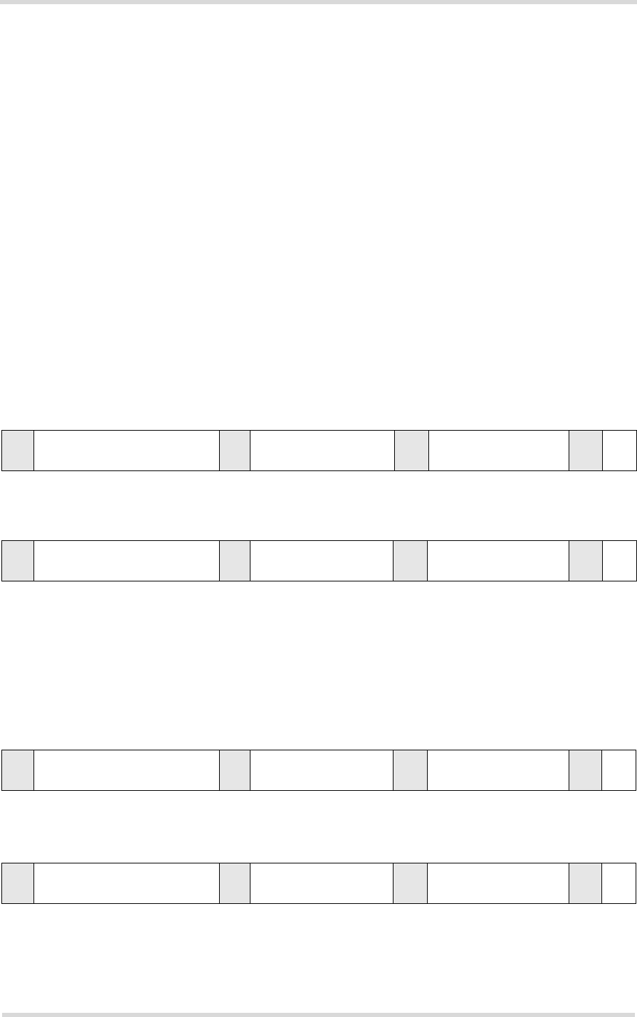
Cinterion® Java Terminals Hardware Interface Description
8.4 Configuration via I2C Interface
69
EHSxT_BGS5T_HID_v02 2014-08-05
Confidential / Preliminary
Page 65 of 70
8.4 Configuration via I2C Interface
While the complete watchdog functionality may be configured via ASC0 interface (for details
see Section 8.3) some of the configuration commands can also be configured during runtime
via I2C interface as described in this section.
The I2C interface is accessible either via the external Weidmueller connector - I2CDAT and
I2CCLK, or via the Java module‘s AT command interface (e.g., ASC0), or through a Java MID-
let during runtime.
The I2C interface implements the write and the read protocol as described in Section 8.4.1. The
7-bit device address is 0x6A (binary: 1101010). The default address can be changed by con-
figuration command (see Section 8.3.1.9).
8.4.1 Command Specification
8.4.1.1 WRITE Command Syntax
Example setting the GPIO12 signal direction to “output” (see also section Examples):
Legend:
S: Start Condition, W: Write bit (=0), A: Acknowledge, P: Stop Condition.
8.4.1.2 READ Command Syntax
Example reading the last status = OK (see also section Examples):
Legend:
S: Start Condition, R: Read bit (=1), A: Acknowledge, N: Not Acknowledge, P: Stop Condition.
S Slave address
(including write bit “W“) A Register address A Data byte AP
S0xD4
(including write bit “0“) A 0x14 A 0x01 AP
S Slave address
(including read bit “R“) A Register address A Data length
(only one byte) NP
S 0xD5
(including read bit “1“) A 0x00 A 0x01
(only one byte) NP
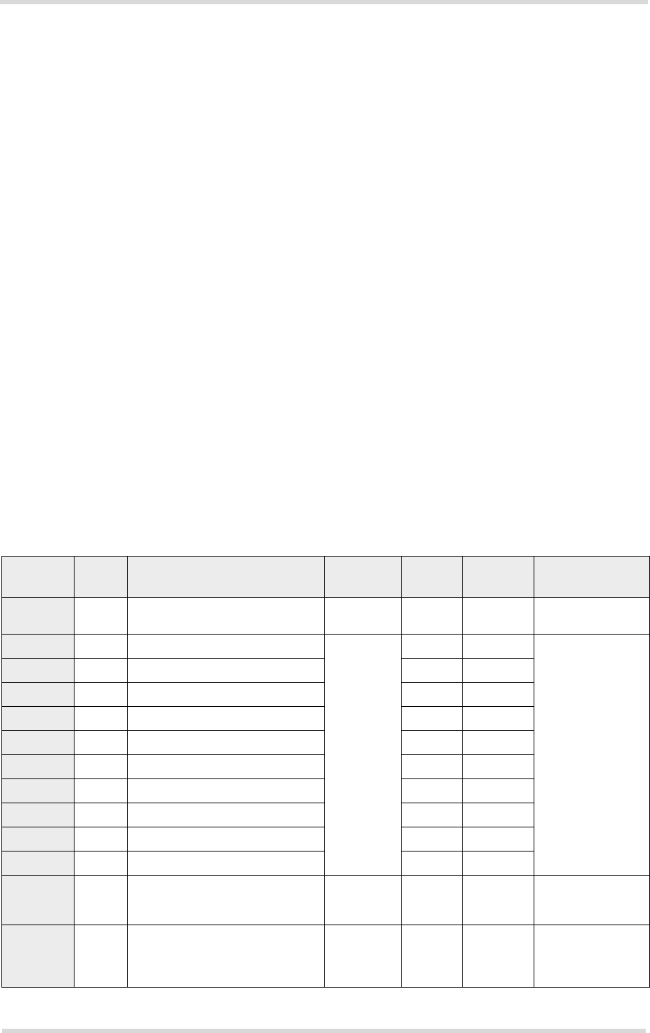
Cinterion® Java Terminals Hardware Interface Description
8.4 Configuration via I2C Interface
69
EHSxT_BGS5T_HID_v02 2014-08-05
Confidential / Preliminary
Page 66 of 70
8.4.1.3 I2C Protocol Overview
In write mode (i.e., slave address “0xD4“), one address byte and one data byte is sent to the
Java Terminal/Watchdog. The address byte specifies a register to write the data byte to. The
data byte value is only written, if it is valid, i.e., in the specified range. After a write attempt, the
status code of the operation is saved and the read address register (RAR) is automatically set
to the status register address (SR). A subsequent read command from the status register (SR)
will then return the latest status code (see Table 26). Only when the address byte is the RAR,
i.e. another register is selected to be read, the RAR is not automatically set to the SR register.
See Section 8.4.1.4 for sample watchdog configurations via I2C.
In read mode, one data byte can be read from the Java Terminal/Watchdog. Attempts to read
more bytes will result in undefined values being returned by the device. The device will always
return the value that is addressed by the RAR. To read a specific register, a write command
with RAR as the address byte and the register to be read as the data byte has to be issued first.
The next read will then return the value at this address. Note that there are only a few registers
that can be read (see register table - Table 25). When the RAR is written with a non-read ad-
dress, the RAR is set to the SR, and the status code ILLEGAL_ARGUMENT is saved. Note
also that a consecutive read is not valid, as the return value will be ILLEGAL_ARGUMENT, but
the caller cannot determine whether the result is the value at the faulty address or an error sta-
tus code. See Section 8.4.1.4 for sample watchdog configurations via I2C.
8.4.1.4 I2C Commands
The following table lists the address register for configuration commands via I2C interface.
Table 25: Address register for I2C commands
Register
address Read/
Write Description Name Non-
volatile Default Value range
0x00 RStatus; only address register to
read directly from. SR -OK See result codes
Table 26
0x10 WGPIO6 GPIOxR Yes 10: Input
1: Output
0x11 WGPIO7 Yes 1
0x12 WGPIO8 Yes 1
0x13 WGPIO11 Yes 1
0x14 WGPIO12 Yes 0
0x15 WGPIO13 Yes 0
0x16 WGPIO14 Yes 0
0x17 WGPIO15 Yes 0
0x18 WGPIO21 Yes 0
0x19 WGPIO20 Yes 1
0x30 RGPIO direction Low Byte:
Read out 8 bits for the GPIOs
[15,14,13,12,11,8,7,6]
GPIOLBR -[0..0xFF]
0x31 RGPIO direction High Byte:
Read out 2 bits for the GPIOs
20 and 21 in the representation:
[0,0,0,0,0,0,<20>,<21>]
GPIOHBR -[0..0xFF]
Cinterion® Java Terminals Hardware Interface Description
8.4 Configuration via I2C Interface
69
EHSxT_BGS5T_HID_v02 2014-08-05
Confidential / Preliminary
Page 67 of 70
Possible result codes for status command (see Section 8.4.1.3 and above Table 25):
0x50 R/W ADC1_IN/DSR0 ADCDSRR Yes 0x00 0: Analog In
1: Digital Out
0x80 WTrigger delay. Specifies delay
time for a reset. If a trigger delay
time is specified, the watchdog is
prevented from resetting the
module for the given time.
TDR No 0x00 Set time in min-
utes.
1...255: Minutes
0: Disable
0xFD RHardware watchdog‘s firmware
version VER -- [0x00..0x99]
[MAJ MIN]
4:MSB: MAJ
4:LSB: MIN
MAJ: Main release
number (e.g., 1.x)
MIN: Sub release
number (e.g., x.0)
as in version v1.0
0xFF WRead address register (RAR) RAR No 0x00 0x00..0xFF
Only valid
addresses contain
valid values
Table 26: I2C status result codes
Result Code Comment
OK 0x00 Last command was executed successfully
PROTOCOL_ERROR 0x01 Protocol error, i.e. wrong number of bytes
ILLEGAL_ADDRESS 0x02 Illegal register address
ILLEGAL_ARGUMENT 0x03 Illegal argument. Argument is out of allowed range.
UNDEFINED 0xFF
Table 25: Address register for I2C commands
Register
address Read/
Write Description Name Non-
volatile Default Value range
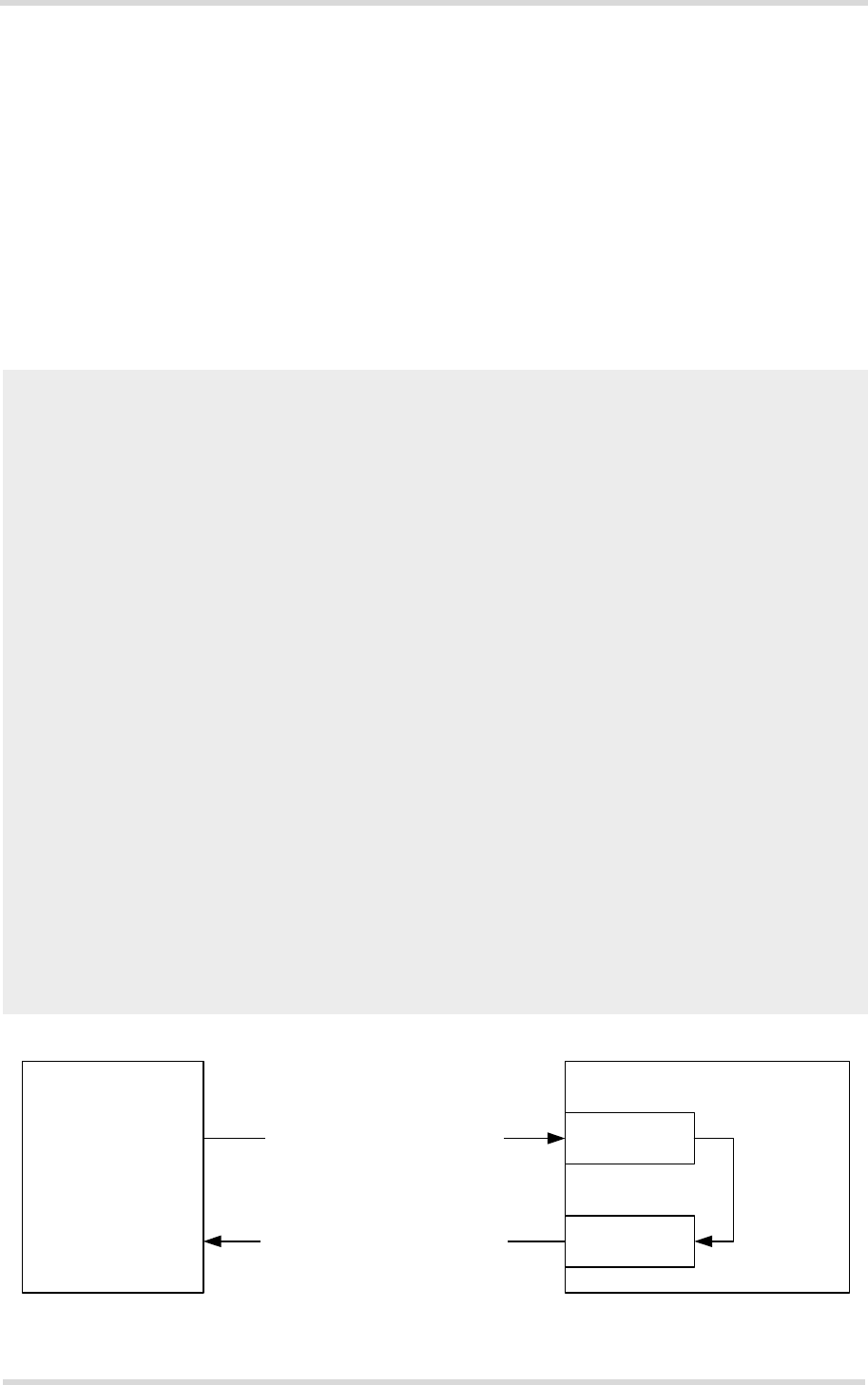
Cinterion® Java Terminals Hardware Interface Description
8.4 Configuration via I2C Interface
69
EHSxT_BGS5T_HID_v02 2014-08-05
Confidential / Preliminary
Page 68 of 70
Examples
The following two samples show how the watchdog can be configured via the I2C interface, us-
ing the AT^SSPI command (at RS-232/ASC0) to transfer the I2C user data. Please refer to [1]
for more information on the AT command AT^SSPI and on how to configure and control the
data transfer over the I2C interface.
The above Table 25 specifies the address register that can be used in I2C configuration com-
mands.
The first example sets GPIO12 to “output“. It therefore configures a write register marked as
“W“ in Table 25.
Figure 18: Write data to address register
AT^SSPI=
CONNECT
<aD41401>
{a+}
<bD50001>
{b+00}
#
OK
Open the Java Terminals I2C data connection.
Indicates that the connection is open.
WRITE command enclosed by <>: “a“ is a command ID to better identify and match
acknowledgments, “D4“ indicates the slave address (write mode), “14“ specifies
the address register GPIO12, and “01“ sets the data byte (i.e., line is “output“).
Note: The data byte value is only written if valid, i.e., if in the specified range. After
a WRITE command, the status code of the operation is saved to the status register
(SR) and a subsequent READ command from the status register will then return
the latest status code as listed in Table 26.
Acknowledgement enclosed in curly brackets of a successful data transmission.
READ command enclosed by <>: “b“ is a command ID to better identify and match
acknowledgements, “D5“ indicates the slave address (read mode), “00“ specifies
the address register SR, and “01“ sets the data length to be read. Note: The READ
command can only be called in conjunction with the SR address “00“ and the data
length of one byte “01“.
Acknowledgement enclosed in curly brackets of a successful data transmission,
together with the response code “00“ indicating that the command was successful-
ly executed.
Close data connection.
Connection closed.
PC Watchdog
Write: Set GPIO12 to “output“ GPIO12:
01
SR:
00
Read from status register (SR)
Command
executed
successfully
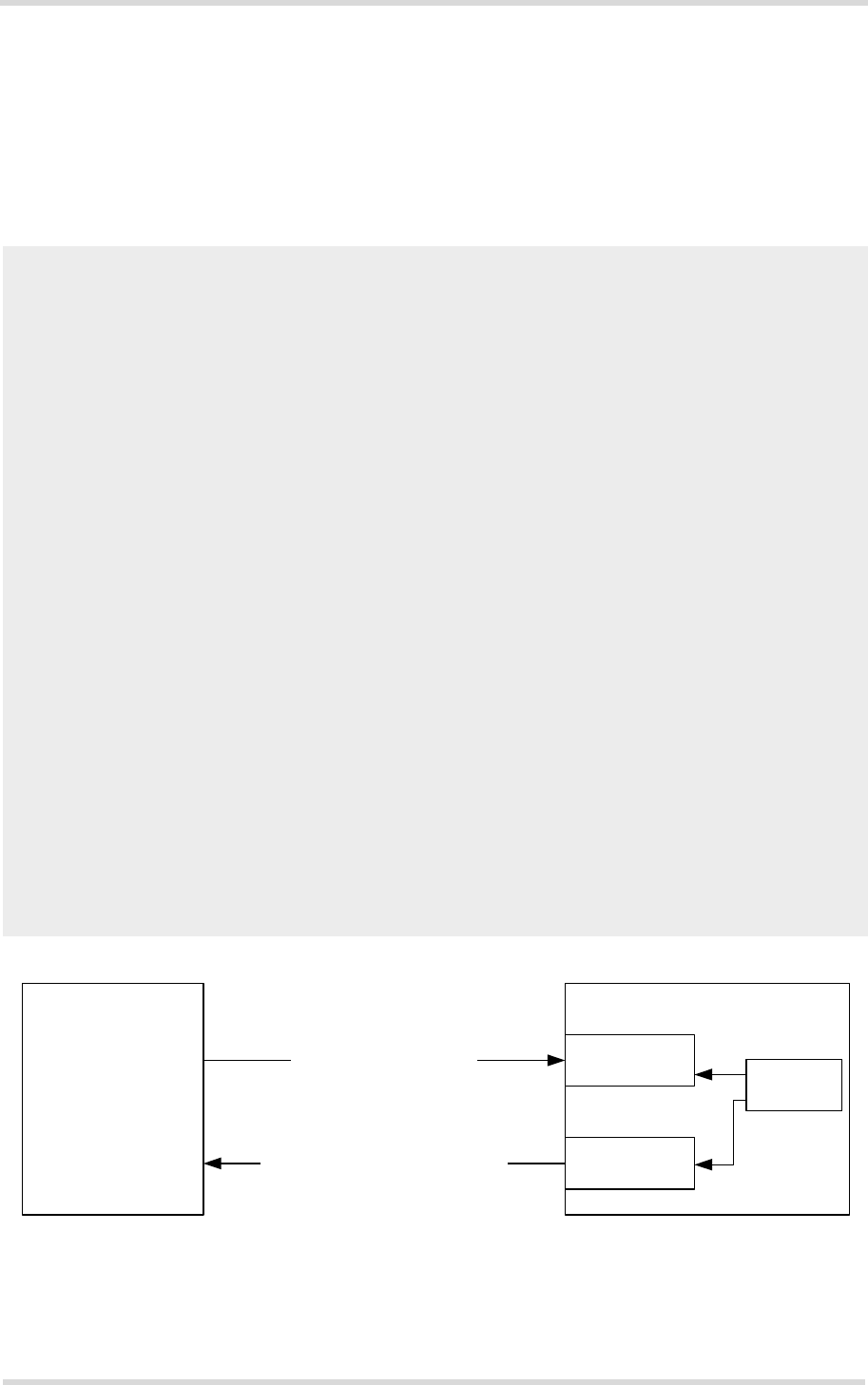
Cinterion® Java Terminals Hardware Interface Description
8.4 Configuration via I2C Interface
69
EHSxT_BGS5T_HID_v02 2014-08-05
Confidential / Preliminary
Page 69 of 70
The second example listed below reads out the firmware version, it therefore uses a read reg-
ister marked as “R“ in Table 25.
However, except for the status address register (SR) no information can be directly retrived
from an address register itself, but only indirectly by means of a so-called read-address-register
(RAR). An initial WRITE command has to link the register to be read to the RAR first. Now the
RAR is linked to the register to be read, and the content of this register can be read from the SR.
Figure 19: Read data from address register
AT^SSPI=
CONNECT
<aD4FFFD>
{a+}
<bD50001>
{b+10}
#
OK
Open the Java Terminals I2C data connection.
Indicates that the connection is open.
WRITE command enclosed by <>: “a“ is a command ID to better identify and match
acknowledgments, “D4“ indicates the slave address (write mode), “FF“ specifies
the read address register RAR, and “FD“ sets the data byte to the watchdogs firm-
ware version register VER (i.e., RAR and VER are linked by this command). Note:
The data byte value is only written if valid, i.e., if in the specified range. After a
WRITE command, the status code of the operation, in this case, i.e., where the
register address is the RAR, the content of the register given as data byte is saved
to the status register (SR) and a subsequent READ command from the status reg-
ister will then return the register value, i.e., the firmware version.
Acknowledgement enclosed in curly brackets of a successful data transmission.
READ command enclosed by <>: “b“ is a command ID to better identify and match
acknowledgements, “D5“ indicates the slave address (read mode), “00“ specifies
the address register SR, and “01“ sets the data length to be read. Note: The READ
command can only be called in conjunction with the SR address “00“ and the data
length of one byte “01“.
Acknowledgement enclosed in curly brackets of a successful data transmission,
together with the response code “10“ indicating that the command was successful-
ly executed. The resposne code gives the watchdog‘s firmware version as v1.0.
Close data connection.
Connection closed.
PC Watchdog
Write: Set RAR to VER RAR:
VER
SR:
01
Read from status register (SR)
Copy
firmware
version to
SR
VER:
01

70
M2M.GEMALTO.COM
About Gemalto
Gemalto (Euronext NL0000400653 GTO) is the world leader in digital security with 2011 annual
revenues of €2 billion and more than 10,000 employees operating out of 74 offices and 14 Research
& Development centers, located in 43 countries.
We are at the heart of the rapidly evolving digital society. Billions of people worldwide increasingly
want the freedom to communicate, travel, shop, bank, entertain and work - anytime, everywhere
- in ways that are enjoyable and safe. Gemalto delivers on their expanding needs for personal
mobile services, payment security, authenticated cloud access, identity and privacy protection,
eHealthcare and eGovernment efficiency, convenient ticketing and dependable machine-to-
machine (M2M) applications.
Gemalto develops secure embedded software and secure products which we design and
personalize. Our platforms and services manage these secure products, the confidential data they
contain and the trusted end-user services they enable. Our inovations enable our clients to offer
trusted and convenient digital services to billions of individuals.
Gemalto thrives with the growing number of people using its solutions to interact with the digital
and wireless world.
For more information please visit
m2m.gemalto.com, www.facebook.com/gemalto, or Follow@gemaltom2m on twitter.
Gemalto M2M GmbH
St.-Martin-Str. 60
81541 Munich
Germany
© Gemalto 2014. All rights reserved. Gemalto, the Gemalto logo, are trademarks and service marks of Gemalto and are registered in certain countries. April 2013