THALES DIS AlS Deutschland PDS8 GSM/WCDMA Module User Manual PDS8 Rev 1
Gemalto M2M GmbH GSM/WCDMA Module PDS8 Rev 1
UserManual.wiki
>
THALES DIS AlS Deutschland
>
PDS8 User Manual
>
PDS8_user manual_Rev 1
Contents
1.
PDS8_user manual_Rev 1
2.
TempConfidential_PDS8_user manual_Rev 1
PDS8_user manual_Rev 1
Navigation menu
Upload a User Manual
Namespaces
Wiki Guide
HTML
PDF
Info
Views
User Manual
Discussion / Help
Navigation
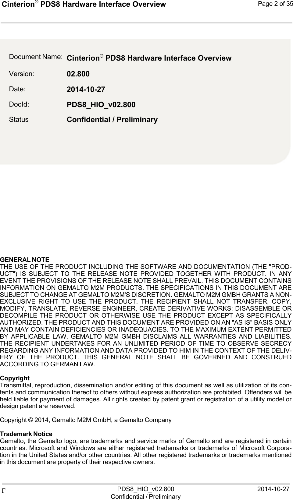
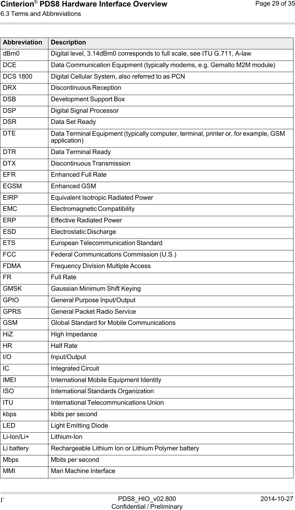
![ PDS8_HIO_v02.800Confidential / Preliminary2014-10-27Cinterion® PDS8 Hardware Interface Overview 1.1 Key Features at a Glance Page 8 of 35 Feature ImplementationSIM Application Toolkit SAT Release 99Firmware update Generic update from host application over ASC0 or USB modem. Interfaces Module interface Surface mount device with solderable connection pads (SMT application interface). Land grid array (LGA) technology ensures high solder joint reli- ability and provides the possibility to use an optional module mounting socket. For more information on how to integrate SMT modules see also [3]. This application note comprises chapters on module mounting and application layout issues as well as on SMT application development equipment. USB USB 2.0 High Speed (480Mbit/s) device interface, Full Speed (12Mbit/s) compliant 1 serial interface ASC0: • 8-wire modem interface with status and control lines, unbalanced, asyn- chronous • Adjustable baud rates: 1,200bps to 921,600bps • Autobauding: 1,200bps to 230,400bps • Supports RTS0/CTS0 hardware flow control. • Multiplex ability according to GSM 07.10 Multiplexer Protocol. Audio 1 digital interface (PCM)UICC interface Supported SIM/USIM cards: 3V, 1.8VGPIO interface 6 GPIOs shared with fast shutdown, pulse counter, and PWM functionalityI2C interface Supports I2C serial interfaceSPI interface Serial peripheral interfaceADC input Analog-to-digital comverter for general purpose voltage measurementsAntenna interface pads 50 Power on/off, Reset Power on/off Switch-on by hardware signal IGT Switch-off by AT command Switch off by hardware signal GPIO4/FST_SHDN instead of AT command Automatic switch-off in case of critical temperature and voltage conditions Reset Orderly shutdown and reset by AT command Emergency reset by hardware signal EMERG_OFF and IGT Special features Real time clock Timer functions via AT commandsPhonebook SIM and phoneTTY/CTM support Integrated CTM modemEvaluation kit Evaluation module PDS8 module soldered onto a dedicated PCB that can be connected to an adapter in order to be mounted onto the DSB75. DSB75 DSB75 Development Support Board designed to test and type approve Gemalto M2M modules and provide a sample configuration for application engineering. A special adapter is required to connect the PDS8 evaluation module to the DSB75.](https://usermanual.wiki/THALES-DIS-AlS-Deutschland/PDS8.PDS8-user-manual-Rev-1/User-Guide-2431071-Page-8.png)
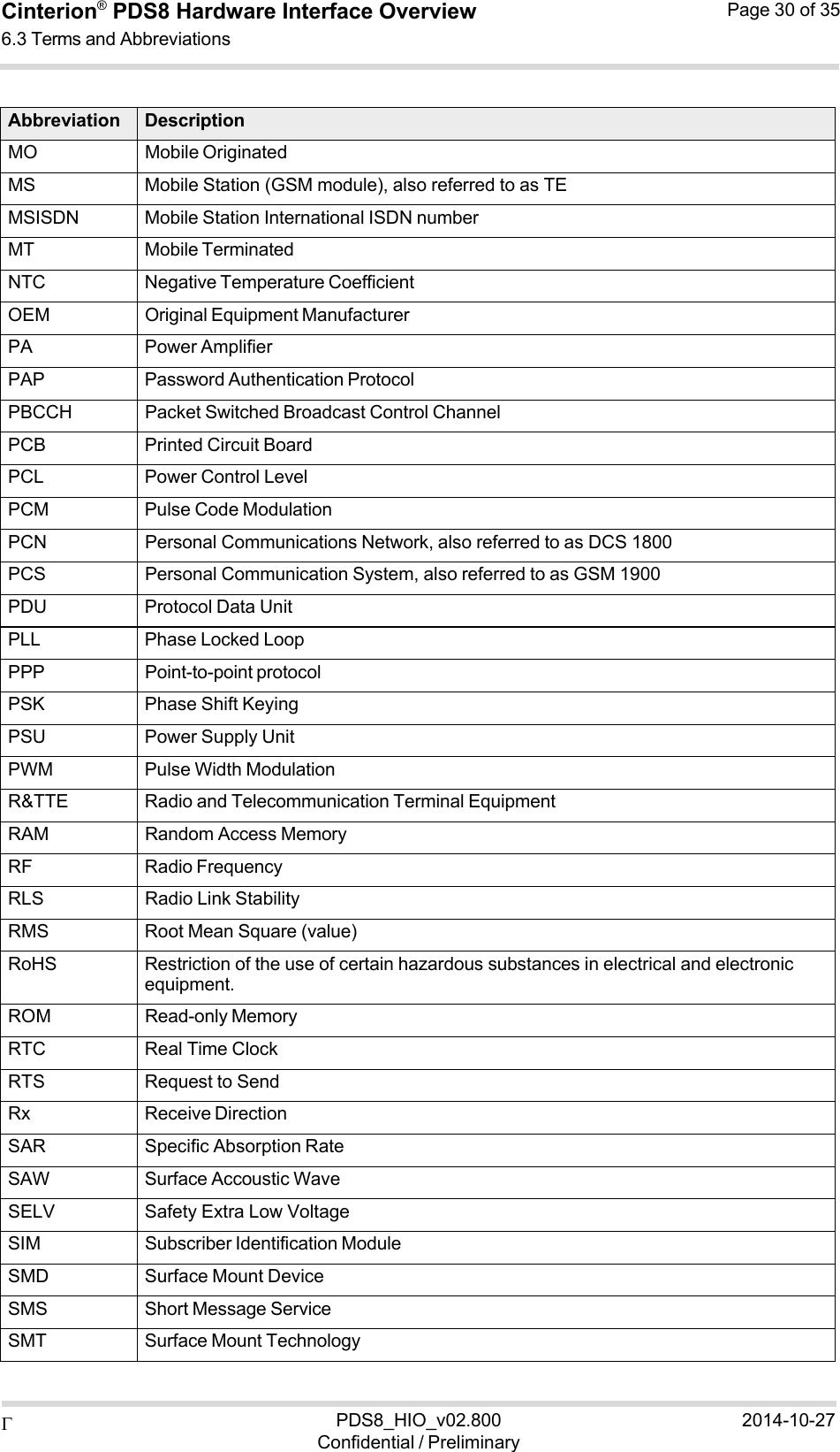
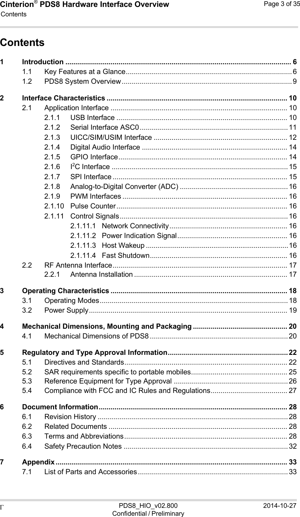
![ PDS8_HIO_v02.800Confidential / Preliminary2014-10-27Cinterion® PDS8 Hardware Interface Overview 2.1 Application Interface Page 14 of 35 2.1.4 Digital Audio Interface PDS8‘s digital audio interface (DAI) can be used to connect audio devices capable of pulse code modulation (PCM). 2.1.5 GPIO Interface PDS8 offers a GPIO interface with 8 GPIO lines. The GPIO lines are shared with other interfaces or functions: Fast shutdown (see Section 2.1.11.4), the PWM functionality (see Section 2.1.9), an pulse counter (see Section 2.1.10). The following table shows the configuration variants for the GPIO pads. All variants are mutu- ally exclusive, i.e. a pad configured for instance as fast shutdown line is locked for alternative usage as GPIO. Table 2: GPIO lines and possible alternative assignment GPIO Fast Shutdown PWM Pulse Counter GPIO2 GPIO4 FST_SHDN GPIO5 GPIO6 PWM2 GPIO7 PWM1 GPIO8 COUNTER GPIO9 GPIO10 After startup, the above mentioned alternative GPIO line assignments can be configured using AT commands (see [1]). The configuration is non-volatile and available after module restart.](https://usermanual.wiki/THALES-DIS-AlS-Deutschland/PDS8.PDS8-user-manual-Rev-1/User-Guide-2431071-Page-14.png)
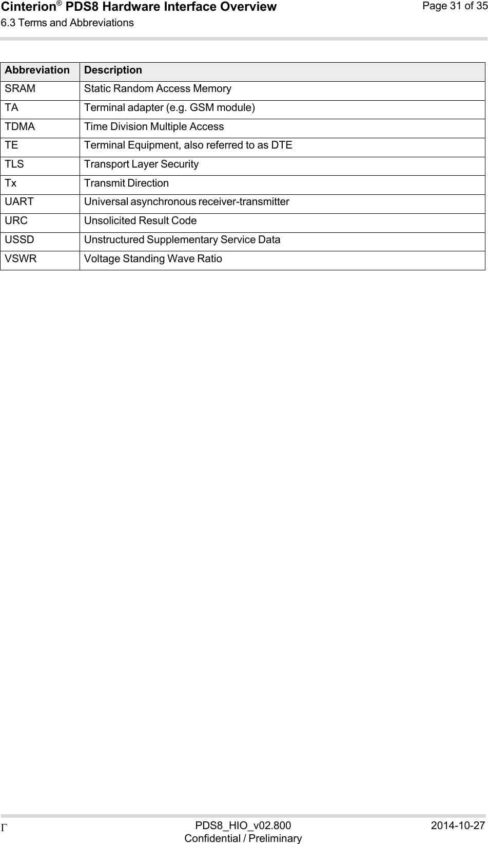
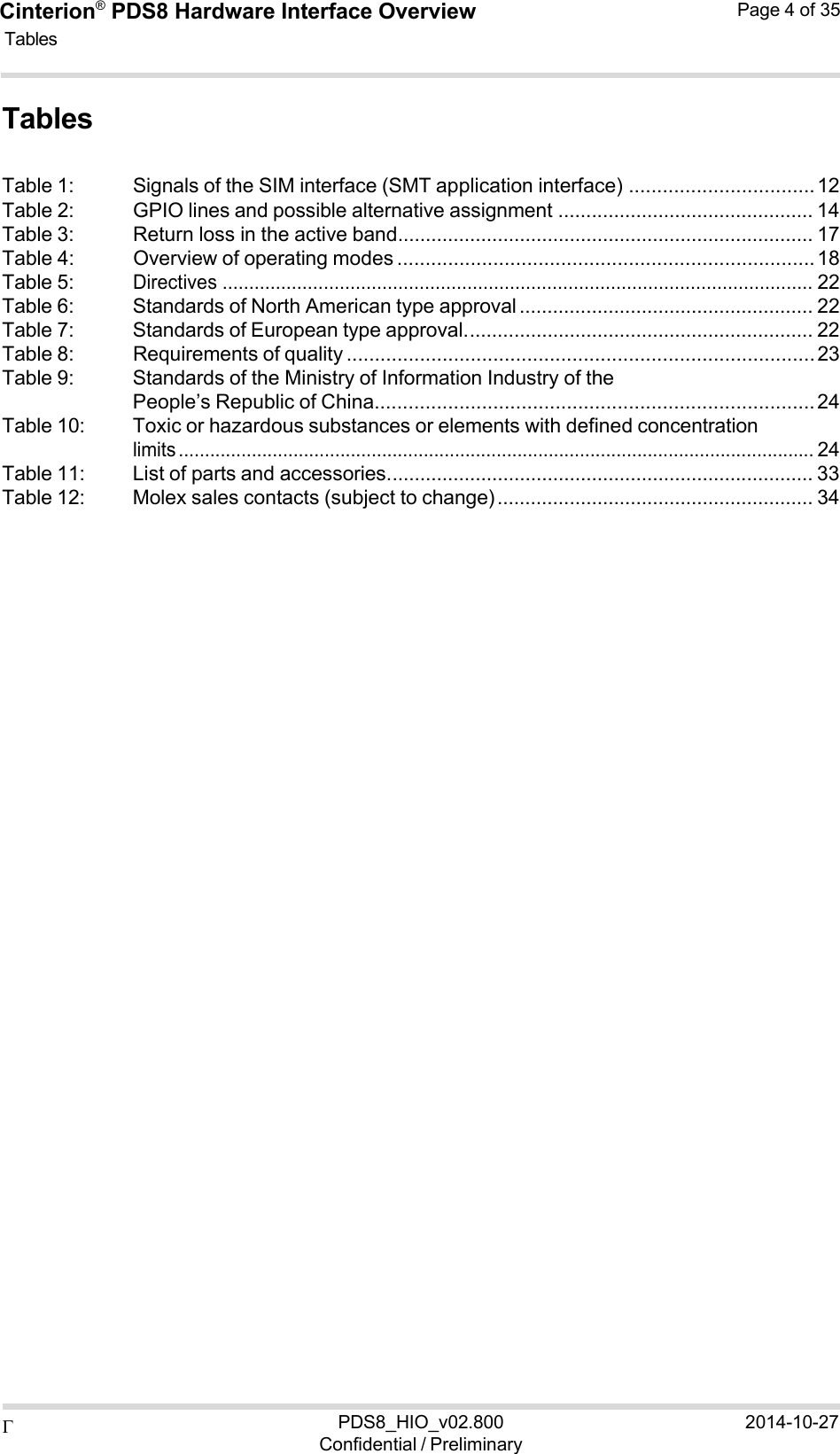
![ PDS8_HIO_v02.800Confidential / Preliminary2014-10-27Cinterion® PDS8 Hardware Interface Overview 2.1 Application Interface Page 16 of 35 2.1.8 Analog-to-Digital Converter (ADC) ADC1_IN is used for general purpose voltage measurements. ADC1_IN can be configured and read by AT command - see [1]. 2.1.9 PWM Interfaces The GPIO6 and GPIO7 interface lines can be configured as Pulse Width Modulation (PWM) interface lines PWM1 and PWM2. The PWM interface lines can be used, for example, to con- nect buzzers. The PWM1 line is shared with GPIO7 and the PWM2 line is shared with GPIO6 (for GPIOs see Section 2.1.5). GPIO and PWM functionality are mutually exclusive. 2.1.10 Pulse Counter The GPIO8 line can be configured as pulse counter line COUNTER. The pulse counter inter- face can be used, for example, as a clock (for GPIOs see Section 2.1.5). 2.1.11 Control Signals 2.1.11.1 Network Connectivity The STATUS line serves to indicate the module’s network connectivity state and can be used to control an externally connected LED. 2.1.11.2 Power Indication Signal The power indication signal PWR_IND notifies the on/off state of the module. High state of PWR_IND indicates that the module is switched off. 2.1.11.3 Host Wakeup If no call, data or message transfer is in progress, the host may shut down its own USB inter- face to save power. If a call or other request (URC’s, messages) arrives, the host can be noti- fied of these events and be woken up again by a state transition of either the RING0 or the GPIO4 line configured as H_WAKEUP line. 2.1.11.4 Fast Shutdown The GPIO4 interface line can be configured as fast shutdown signal line FST_SHDN. The con- figured FST_SHDN line is an active low control signal and must be applied for at least TBD. milliseconds. If unused this line can be left open because of a configured internal pull-up resistor.](https://usermanual.wiki/THALES-DIS-AlS-Deutschland/PDS8.PDS8-user-manual-Rev-1/User-Guide-2431071-Page-16.png)
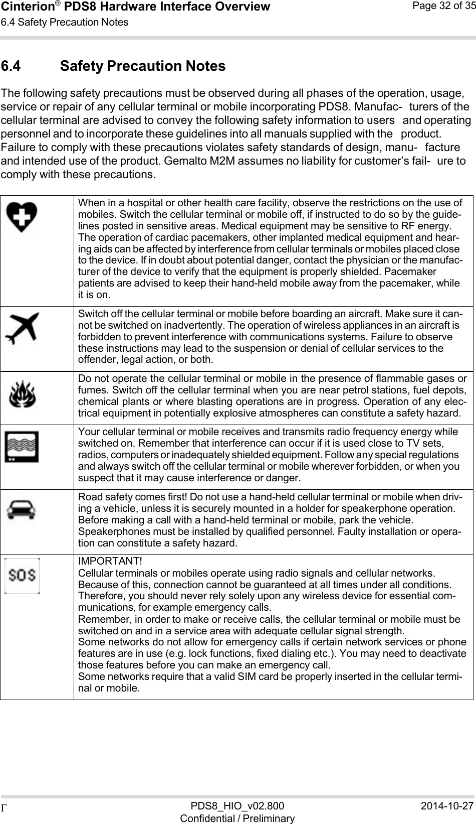
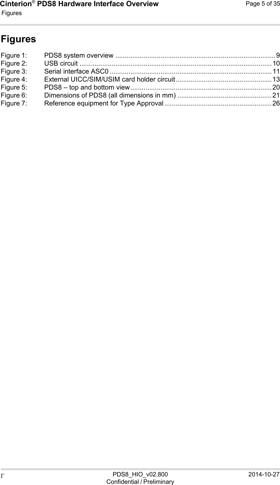
![ PDS8_HIO_v02.800Confidential / Preliminary2014-10-27Cinterion® PDS8 Hardware Interface Overview 3 Operating Characteristics Page 18 of 35 3 Operating Characteristics 3.1 Operating Modes The table below briefly summarizes the various operating modes referred to throughout the document. Table 4: Overview of operating modes Mode Function Normal operation GSM / GPRS / UMTS / HSPA SLEEP No call is in progress and the USB connection is suspended by host (or is not present) and no active communication via ASC0. GSM / GPRS / UMTS / HSPA IDLE No call is in progress and the USB connection is not suspended by host (or is not present) and no active communication via ASC0. GSM TALK/ GSM DATA Connection between two subscribers is in progress. Power consump- tion depends on the GSM network coverage and several connection settings (e.g. DTX off/on, FR/EFR/HR, hopping sequences and antenna connection). The following applies when power is to be mea- sured in TALK_GSM mode: DTX off, FR and no frequency hopping. GPRS DATA GPRS data transfer in progress. Power consumption depends on net-work settings (e.g. power control level), uplink / downlink data rates and GPRS configuration (e.g. used multislot settings). EGPRS DATA EGPRS data transfer in progress. Power consumption depends on net-work settings (e.g. power control level), uplink / downlink data rates andEGPRS configuration (e.g. used multislot settings). UMTS TALK/ UMTS DATA UMTS data transfer in progress. Power consumption depends on net- work settings (e.g. TPC Pattern) and data transfer rate. HSPA DATA HSPA data transfer in progress. Power consumption depends on net- work settings (e.g. TPC Pattern) and data transfer rate. Power Down Normal shutdown after sending the power down command. Only a voltage regulator is active for powering the RTC. Software is not active. Interfaces are not accessible. Operat- ing voltage (connected to BATT+) remains applied. Airplane mode Airplane mode shuts down the radio part of the module, causes the module to log off fromthe GSM/GPRS network and disables all AT commands whose execution requires a radioconnection. Airplane mode can be controlled by AT command (see [1]).](https://usermanual.wiki/THALES-DIS-AlS-Deutschland/PDS8.PDS8-user-manual-Rev-1/User-Guide-2431071-Page-18.png)
![ PDS8_HIO_v02.800Confidential / Preliminary2014-10-27Cinterion® PDS8 Hardware Interface Overview 6 Document Information Page 28 of 35 6 Document Information 6.1 Revision History New document: "Cinterion® PDS8 Hardware Interface Overview" Version 01.000 Chapter What is new -- Initial document setup. 6.2 Related Documents [1] PDS8 AT Command Set [2] PDS8 Release Note [3] Application Note 48: SMT Module Integration [4] Universal Serial Bus Specification Revision 2.0, April 27, 2000 6.3 Terms and Abbreviations Abbreviation Description ADC Analog-to-digital converterAGC Automatic Gain ControlANSI American National Standards InstituteARFCN Absolute Radio Frequency Channel NumberARP Antenna Reference PointASC0/ASC1 Asynchronous Controller. Abbreviations used for first and second serial interface of PDS8 B Thermistor Constant BER Bit Error Rate BTS Base Transceiver StationCB or CBM Cell Broadcast MessageCE Conformité Européene (European Conformity)CHAP Challenge Handshake Authentication ProtocolCPU Central Processing UnitCS Coding Scheme CSD Circuit Switched Data CTS Clear to Send DAC Digital-to-Analog ConverterDAI Digital Audio Interface](https://usermanual.wiki/THALES-DIS-AlS-Deutschland/PDS8.PDS8-user-manual-Rev-1/User-Guide-2431071-Page-29.png)