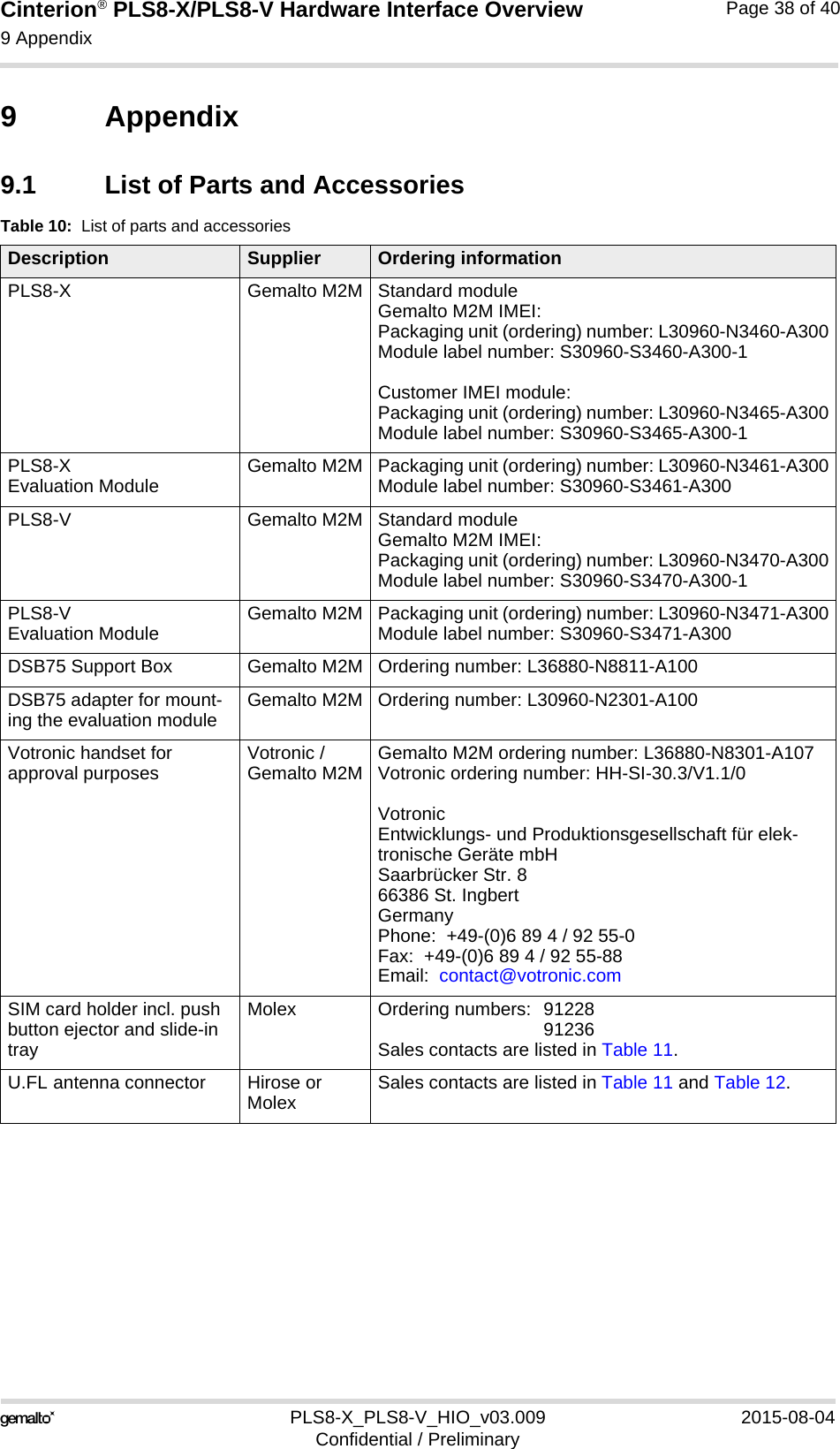
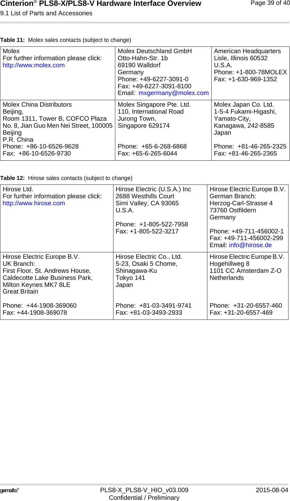
THALES DIS AlS Deutschland PLS8-V LTE Module User Manual hid pls8 x v
Gemalto M2M GmbH LTE Module hid pls8 x v
UserManual.wiki
>
THALES DIS AlS Deutschland
>
PLS8 V User Manual
User Manual
Navigation menu
Upload a User Manual
Namespaces
Wiki Guide
HTML
PDF
Info
Views
User Manual
Discussion / Help
Navigation
![Cinterion® PLS8-X/PLS8-V Hardware Interface Overview1 Introduction13PLS8-X_PLS8-V_HIO_v03.009 2015-08-04Confidential / PreliminaryPage 7 of 401 IntroductionThe document1 describes the hardware of the two Cinterion® modules variants PLS8-V and PLS8-X, designed to connect to a cellular device application and the air interface. It helps you quickly retrieve interface specifications, electrical and mechanical details and information on the requirements to be considered for integrating further components.The product variants differ in their radio access technology support: • PLS8-X is available for operation in LTE, UMTS and GSM radio networks - for supportedfrequency bands please refer to Section 2.1. Connected to this, the module has two sepa-rate firmware images on board that can be activated based on the used (U)SIM card.Employing the module’s two (U)SIM interfaces, it is thus possible to switch between firm-ware images on the fly - making PLS8-X a multi carrier/provider module.• PLS8-V in contrast is available for operation in LTE radio networks only - for supported fre-quency bands please refer to Section 2.1. It has only a single firmware image on board thatcan be activated by (U)SIM card - making it a single carrier/provider module. If not otherwise mentioned, this document applies to both product variants. Where necessary a note is made to differentiate between the variants.1.1 Supported ProductsThis document applies to the following Gemalto M2M products:•Cinterion® PLS8-V module•Cinterion® PLS8-X module1.2 Related Documents[1] AT Command Set for your Gemalto M2M product[2] Release Notes for your Gemalto M2M product[3] Application Note 48: SMT Module Integration[4] Universal Serial Bus Specification Revision 2.0, April 27, 20001.3 Terms and Abbreviations1. The document is effective only if listed in the appropriate Release Notes as part of the technicaldocumentation delivered with your Gemalto M2M product.Abbreviation DescriptionANSI American National Standards InstituteARP Antenna Reference PointCE Conformité Européene (European Conformity)CS Coding SchemeCS Circuit SwitchedCSD Circuit Switched Data](https://usermanual.wiki/THALES-DIS-AlS-Deutschland/PLS8-V/User-Guide-2704179-Page-7.png)
![Cinterion® PLS8-X/PLS8-V Hardware Interface Overview2.1 Key Features at a Glance17PLS8-X_PLS8-V_HIO_v03.009 2015-08-04Confidential / PreliminaryPage 15 of 40UMTS features3GPP Release 8 PS data rate – 384 kbps DL / 384 kbps ULGSM / GPRS / EGPRS featuresData transfer GPRS:• Multislot Class 12• Mobile Station Class B• Coding Scheme 1 – 4EGPRS:• Multislot Class 12• EDGE E2 power class for 8 PSK• Downlink coding schemes – CS 1-4, MCS 1-9• Uplink coding schemes – CS 1-4, MCS 1-9• SRB loopback and test mode B• 8-bit, 11-bit RACH• 1 phase/2 phase access procedures• Link adaptation and IR• NACC, extended UL TBF• Mobile Station Class BSMS Point-to-point MT and MOCell broadcastText and PDU modeSoftwareAT commands Hayes, 3GPP TS 27.007 and 27.005, and proprietary Gemalto M2M com-mandsFirmware update Generic update from host application over USB and ASC0GNSS FeaturesProtocol NMEAModes Standalone GNSSAssisted GNSS- Control plane - E911- User plane - gpsOneXTRA™General Power saving modesPower supply for active antennaInterfacesModule interface Surface mount device with solderable connection pads (SMT application interface).Land grid array (LGA) technology ensures high solder joint reliability and provides the possibility to use an optional module mounting socket.For more information on how to integrate SMT modules see also [3]. This application note comprises chapters on module mounting and application layout issues as well as on additional SMT application development equipment.Antenna 50. GSM/UMTS/LTE main antenna, UMTS/LTE Diversity/MIMO antenna, (active/passive) GNSS antennaUSB USB 2.0 High Speed (480Mbit/s) device interfaceFeature Implementation](https://usermanual.wiki/THALES-DIS-AlS-Deutschland/PLS8-V/User-Guide-2704179-Page-15.png)
![Cinterion® PLS8-X/PLS8-V Hardware Interface Overview3.1 Operating Modes26PLS8-X_PLS8-V_HIO_v03.009 2015-08-04Confidential / PreliminaryPage 19 of 403.1 Operating ModesThe table below briefly summarizes the various operating modes referred to in the following chapters.Table 6: Overview of operating modesMode FunctionNormal operation GSM / GPRS / UMTS / HSPA /LTE SLEEPPower saving set automatically when no call is in progress and the USB connection is detached and no active communication via ASC0. Also, the GNSS active antenna mode has to be turned off or set to "auto".GSM / GPRS / UMTS / HSPA / LTE IDLEPower saving disabled or an USB connection active, but no data trans-fer in progress.GPRS DATA GPRS data transfer in progress. Power consumption depends on net-work settings (e.g. power control level), uplink / downlink data rates and GPRS configuration (e.g. used multislot settings).EGPRS DATA EGPRS data transfer in progress. Power consumption depends on net-work settings (e.g. power control level), uplink / downlink data rates and EGPRS configuration (e.g. used multislot settings).UMTS DATA UMTS data transfer in progress. Power consumption depends on net-work settings (e.g. TPC Pattern) and data transfer rate.HSPA DATA HSPA data transfer in progress. Power consumption depends on net-work settings (e.g. TPC Pattern) and data transfer rate.LTE DATA LTE data transfer in progress. Power consumption depends on network settings (e.g. TPC Pattern) and data transfer rate.Power Down Normal shutdown after sending the AT^SMSO command. Only a voltage regulator is active for powering the RTC. Software is not active. Interfaces are not accessible. Operating volt-age (connected to BATT+) remains applied.Airplane mode Airplane mode shuts down the radio part of the module, causes the module to log off from the GSM/GPRS network and disables all AT commands whose execution requires a radio connection.Airplane mode can be controlled by AT command (see [1]).](https://usermanual.wiki/THALES-DIS-AlS-Deutschland/PLS8-V/User-Guide-2704179-Page-19.png)
![Cinterion® PLS8-X/PLS8-V Hardware Interface Overview3.4 Serial Interface ASC026PLS8-X_PLS8-V_HIO_v03.009 2015-08-04Confidential / PreliminaryPage 22 of 403.4 Serial Interface ASC0PLS8-X/PLS8-V offers an 8-wire unbalanced, asynchronous modem interface ASC0 conform-ing to ITU-T V.24 protocol DCE signalling. The electrical characteristics do not comply with ITU-T V.28. The significant levels are 0V (for low data bit or active state) and 1.8V (for high data bit or inactive state). PLS8-X/PLS8-V is designed for use as a DCE. Based on the conventions for DCE-DTE con-nections it communicates with the customer application (DTE) using the following signals:• Port TXD @ application sends data to the module’s TXD0 signal line• Port RXD @ application receives data from the module’s RXD0 signal lineFigure 4: Serial interface ASC0Features:• Includes the data lines TXD0 and RXD0, the status lines RTS0 and CTS0 and, in addition,the modem control lines DTR0, DSR0, DCD0 and RING0.• The RING0 signal serves to indicate incoming calls and other types of URCs (UnsolicitedResult Code). It can also be used to send pulses to the host application, for example towake up the application from power saving state. See [1] for details on how to configure theRING0 line by AT^SCFG.• Configured for 8 data bits, no parity and 1 stop bit. • ASC0 can be operated at fixed bit rates from 115,200bps up to 921,600bps.• Supports RTS0/CTS0 hardware flow control.• Wake up from SLEEP mode by RTS0 activation.Note: If the ASC0 serial interface is the application’s only interface, it is suggested to connect test points on the USB signal lines as a potential tracing possibility.](https://usermanual.wiki/THALES-DIS-AlS-Deutschland/PLS8-V/User-Guide-2704179-Page-22.png)
![Cinterion® PLS8-X/PLS8-V Hardware Interface Overview3.6 Digital Audio Interface26PLS8-X_PLS8-V_HIO_v03.009 2015-08-04Confidential / PreliminaryPage 25 of 403.6 Digital Audio InterfacePLS8-X/PLS8-V supports a digital audio interface that can be employed either as pulse code modulation interface or as inter IC sound interface. Operation of these interface variants is mu-tually exclusive, and can be configured by AT command (see [1]). Default setting is pulse code modulation.Note: As PLS8-X/PLS8-V is a data only module, the module’s digital audio interface supports local tones only and is otherwise reserved for future use.3.7 Analog-to-Digital Converter (ADC)PLS8-X/PLS8-V provides three unbalanced ADC input lines: ADC1_IN, ADC2_IN and ADC3_IN. They can be used to measure three independent, externally connected DC voltages in the range of 0.3V to 3.075V. 3.8 GPIO InterfacePLS8-X/PLS8-V has 10 GPIOs for external hardware devices. Each GPIO can be configured for use as input or output. All settings are AT command controlled.](https://usermanual.wiki/THALES-DIS-AlS-Deutschland/PLS8-V/User-Guide-2704179-Page-25.png)
![Cinterion® PLS8-X/PLS8-V Hardware Interface Overview4 GNSS Receiver26PLS8-X_PLS8-V_HIO_v03.009 2015-08-04Confidential / PreliminaryPage 26 of 404 GNSS ReceiverPLS8-X/PLS8-V integrates a GNSS receiver that offers the full performance of GPS/GLONASS technology. The GNSS receiver is able to continuously track all satellites in view, thus providing accurate satellite position data.The integrated GNSS receiver supports the NMEA protocol via USB or ASC0 interface. NMEA is a combined electrical and data specification for communication between various (marine) electronic devices including GNSS receivers. It has been defined and controlled by the US based National Marine Electronics Association. For more information on the NMEA Standard please refer to http://www.nmea.org.Depending on the receiver’s knowledge of last position, current time and ephemeris data, the receiver’s startup time (i.e., TTFF = Time-To-First-Fix) may vary: If the receiver has no knowl-edge of its last position or time, a startup takes considerably longer than if the receiver has stillknowledge of its last position, time and almanac or has still access to valid ephimeris data andthe precise time.By default, the GNSS receiver is switched off. It has to be switched on and configured using ATcommands. For more information on how to control the GNSS interface via the AT commands see [1].](https://usermanual.wiki/THALES-DIS-AlS-Deutschland/PLS8-V/User-Guide-2704179-Page-26.png)
![Cinterion® PLS8-X/PLS8-V Hardware Interface Overview5 Antenna Interfaces30PLS8-X_PLS8-V_HIO_v03.009 2015-08-04Confidential / PreliminaryPage 27 of 405 Antenna Interfaces5.1 GSM/UMTS/LTE Antenna InterfaceThe PLS8-X/PLS8-V GSM/UMTS/LTE antenna interface comprises a GSM/UMTS/LTE main antenna as well as a UMTS/LTE Rx diversity/MIMO antenna to improve signal reliability and quality1. The interface has an impedance of 50. PLS8-X/PLS8-V is capable of sustaining a total mismatch at the antenna interface without any damage, even when transmitting at maxi-mum RF power.The external antennas must be matched properly to achieve best performance regarding radi-ated power, modulation accuracy and harmonic suppression. Matching networks are not in-cluded on the PLS8-X/PLS8-V PCB and should be placed in the host application, if the antenna does not have an impedance of 50.Regarding the return loss PLS8-X/PLS8-V provides the following values in the active band:1. By delivery default the UMTS/LTE Rx diversity/MIMO antenna is configured as available for the modulesince its usage is mandatory for LTE. Please refer to [1] for details on how to configure antenna settings. Table 8: Return loss in the active bandState of module Return loss of module Recommended return loss of applicationReceive > 8dB > 12dBTransmit not applicable > 12dBIdle < 5dB not applicable](https://usermanual.wiki/THALES-DIS-AlS-Deutschland/PLS8-V/User-Guide-2704179-Page-27.png)
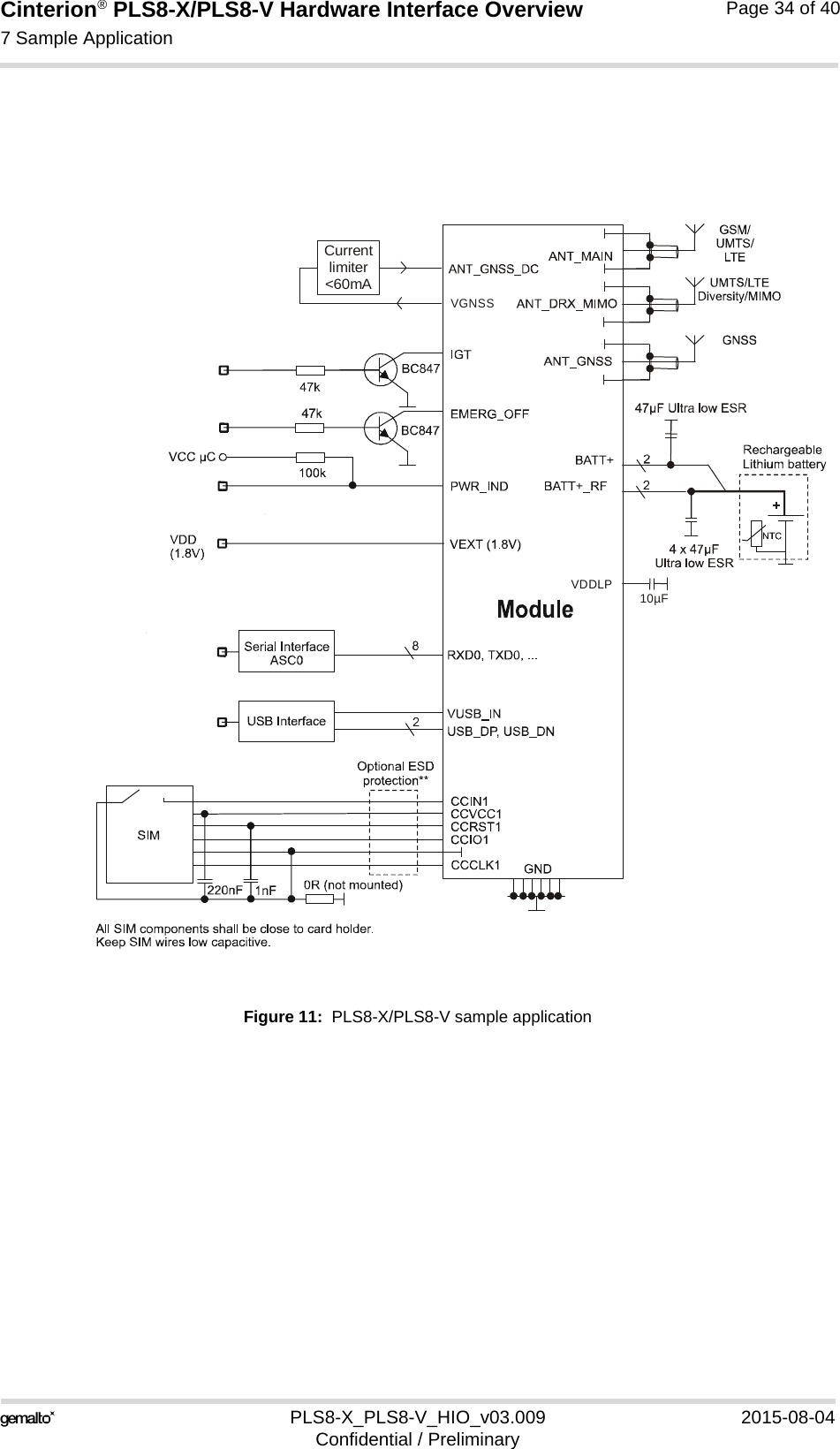
![Cinterion® PLS8-X/PLS8-V Hardware Interface Overview7 Sample Application34PLS8-X_PLS8-V_HIO_v03.009 2015-08-04Confidential / PreliminaryPage 33 of 407 Sample ApplicationFigure 11 shows a typical example of how to integrate an PLS8-X/PLS8-V module with an ap-plication. The PWR_IND line is an open collector that needs an external pull-up resistor which connects to the voltage supply VCC µC of the microcontroller. Low state of the open collector pulls the PWR_IND signal low and indicates that the PLS8-X/PLS8-V module is active, high level notifies the Power Down mode. If the module is in Power Down mode avoid current flowing from any other source into the mod-ule circuit, for example reverse current from high state external control lines. Therefore, the controlling application must be designed to prevent reverse flow.While developing SMT applications it is strongly recommended to provide test pointsfor certain signals, i.e., lines to and from the module - for debug and/or test purposes.The SMT application should allow for an easy access to these signals. For details onhow to implement test points see [3].The EMC measures are best practice recommendations. In fact, an adequate EMC strategy for an individual application is very much determined by the overall layout and, especially, the po-sition of components. Some LGA pads are connected to clocks or high speed data streams that might interfere with the module’s antenna. The RF receiver would then be blocked at certain frequencies (self in-terference). The external application’s PCB tracks connected to these pads should therefore be well shielded or kept away from the antenna. This applies especially to the USB and UICC/SIM interfaces.Disclaimer:No warranty, either stated or implied, is provided on the sample schematic diagram shown in Figure 11 and the information detailed in this section. As functionality and compliance with na-tional regulations depend to a great amount on the used electronic components and the indi-vidual application layout manufacturers are required to ensure adequate design and operating safeguards for their products using PLS8-X/PLS8-V modules.](https://usermanual.wiki/THALES-DIS-AlS-Deutschland/PLS8-V/User-Guide-2704179-Page-33.png)