THALES DIS AlS Deutschland XT65 Quadband GSM/GPRS/GPS Module User Manual XT65 XT75 Hardware Interface Overview
Gemalto M2M GmbH Quadband GSM/GPRS/GPS Module XT65 XT75 Hardware Interface Overview
UserManual.wiki
>
THALES DIS AlS Deutschland
>
XT65 User Manual
User Manual
Navigation menu
Upload a User Manual
Namespaces
Wiki Guide
HTML
PDF
Info
Views
User Manual
Discussion / Help
Navigation
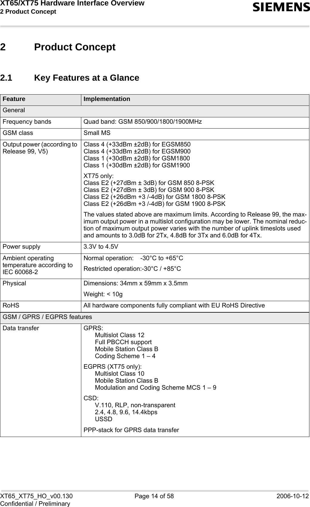
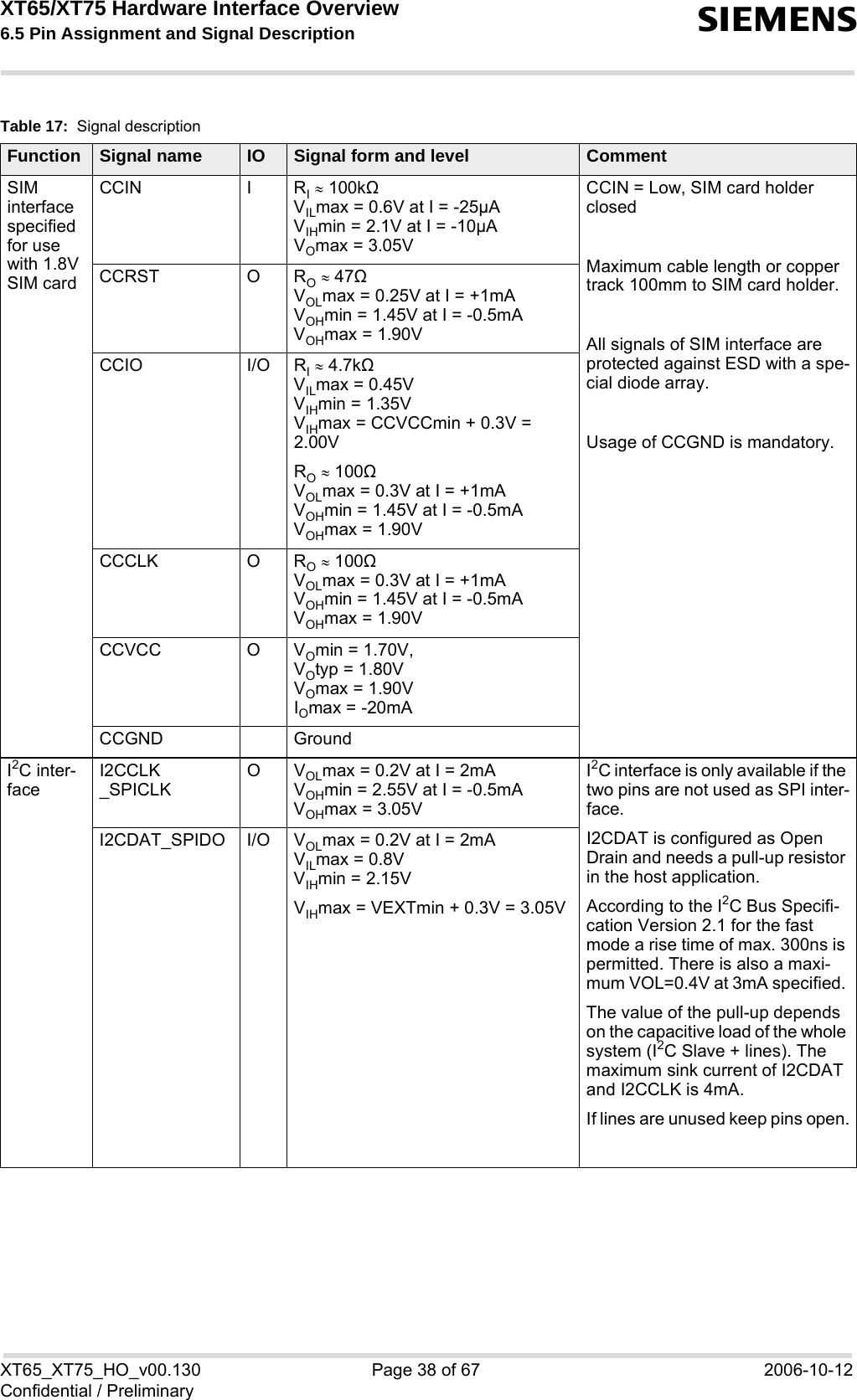
![XT65/XT75 Hardware Interface Overview 1 Introduction sXT65_XT75_HO_v00.130 Page 6 of 67 2006-10-12Confidential / Preliminary1 IntroductionThis document applies to the following Siemens products:• XT65 Module• XT75 ModuleThe document describes the hardware of the XT65 and XT75 modules, both designed to connect to a cellulardevice application and the air interface. It helps you quickly retrieve interface specifications, electrical andmechanical details and information on the requirements to be considered for integrating further components.The difference between both modules is that the XT75 additionally features EGPRS. Please note that except forEGPRS specific statements, all information provided below applies to both module types. Throughout the document, both modules are generally referred to as XT65/XT75.1.1 Related Documents[1] XT65 AT Command Set 00.130XT75 AT Command Set 00.130[2] XT65/XT75 Release Notes 00.130[3] DSB75 Support Box - Evaluation Kit for Siemens Cellular Engines [4] Application Note 02: Audio Interface Design for GSM Applications[5] Application Note 07: Rechargeable Lithium Batteries in GSM Applications [6] Application Note 16: Upgrading Firmware [7] Application Note 17: Over-The-Air Firmware Update [8] Application Note 22: Using TTY / CTM Equipment[9] Application Note 24: Application Developer’s Guide [10] Application Note 26: Power Supply Design for GSM Applications[11] Application Note 32: Integrating USB into GSM Applications[12] Multiplexer User's Guide [13] Multiplex Driver Developer’s Guide for Windows 2000 and Windows XP [14] Multiplex Driver Installation Guide for Windows 2000 and Windows XP [15] Remote SAT User's Guide [16] Java User’s Guide [17] Java doc \wtk\doc\html\index.html](https://usermanual.wiki/THALES-DIS-AlS-Deutschland/XT65/User-Guide-722394-Page-6.png)
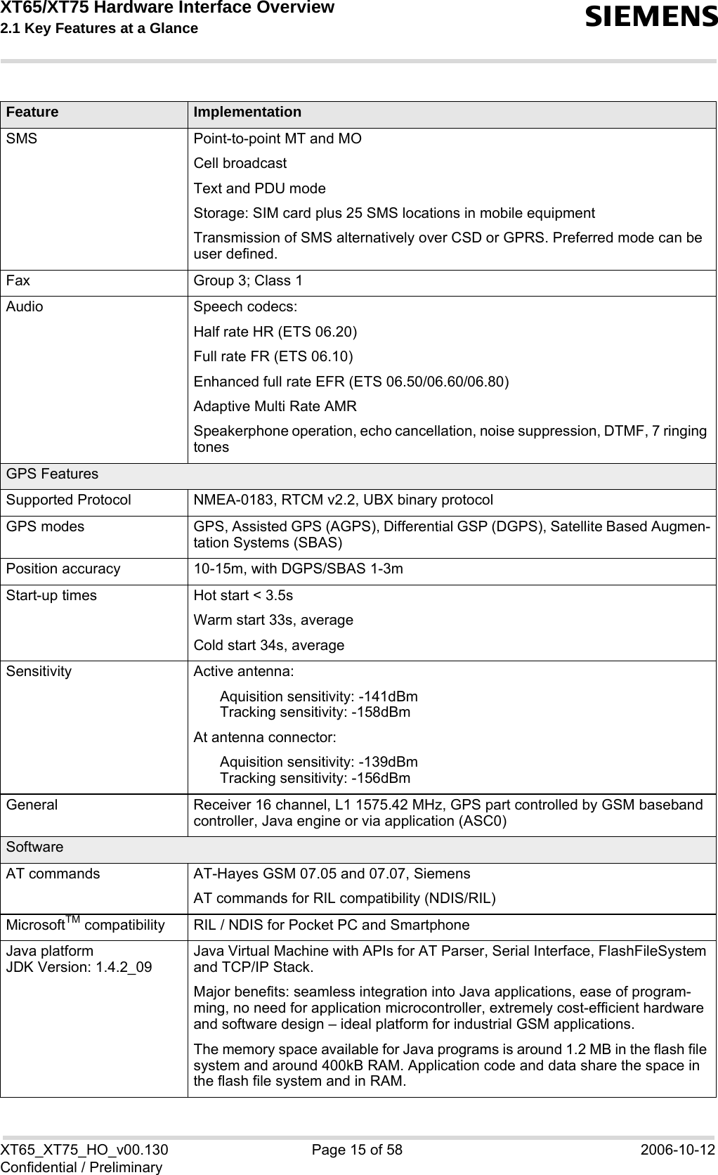
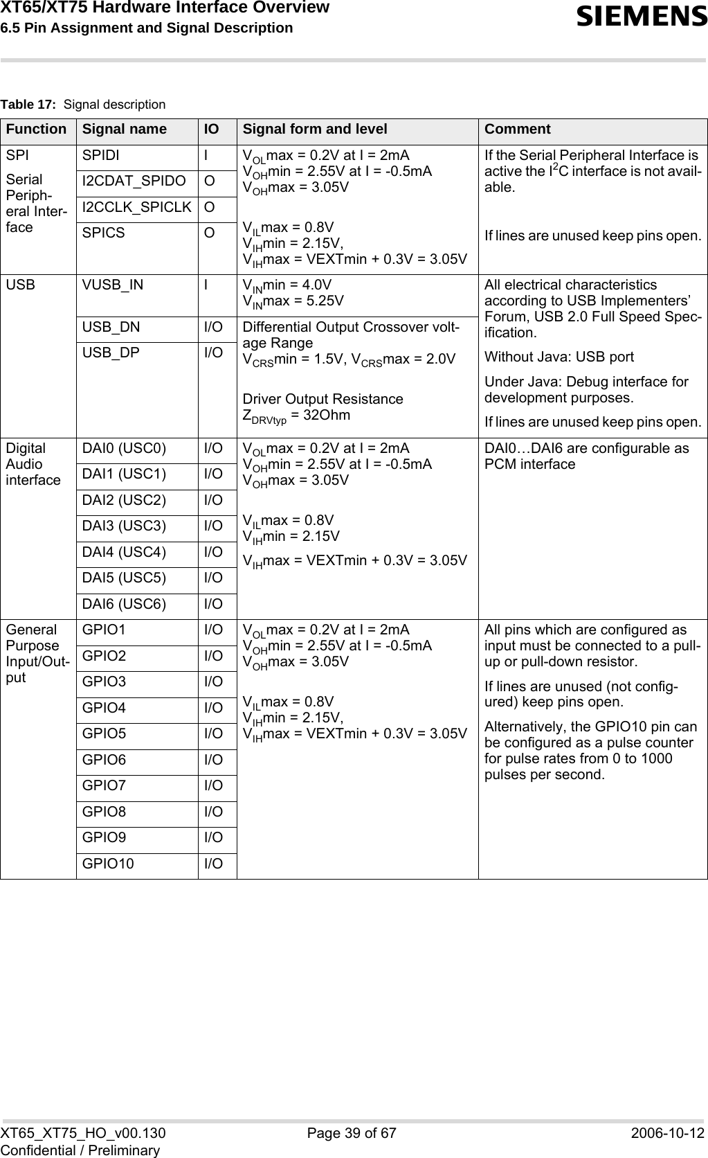
![XT65/XT75 Hardware Interface Overview 8.2 Compliance with FCC Rules and Regulations sXT65_XT75_HO_v00.130 Page 52 of 67 2006-10-12Confidential / Preliminary8.2 Compliance with FCC Rules and Regulations The Equipment Authorization Certification for the Siemens reference application described in Section 8.1 will beregistered under the following identifiers:FCC Identifier: QIPXT65Industry Canada Certification Number: 267W-XT65Granted to Siemens AGFCC Identifier QIPXT75Industry Canada Certification Number: 267W-XT75Granted to Siemens AG Manufacturers of mobile or fixed devices incorporating XT65/XT75 modules are authorized to use the FCCGrants and Industry Canada Certificates of the XT65/XT75 modules for their own final products according to theconditions referenced in these documents. In this case, the FCC label of the module shall be visible from theoutside, or the host device shall bear a second label stating "Contains FCC ID QIP XT65" resp. "Contains FCCID QIP XT75".IMPORTANT:Manufacturers of portable applications incorporating XT65/XT75 modules are required to have their final productcertified and apply for their own FCC Grant and Industry Canada Certificate related to the specific portablemobile. This is mandatory to meet the SAR requirements for portable mobiles (see Section 1.3.2 for detail).Changes or modifications not expressly approved by the party responsible for compliance could void the user'sauthority to operate the equipment.If the final product is not approved for use in U.S. territories the application manufacturer shall take care that the850 MHz and 1900 MHz frequency bands be deactivated and that band settings be inaccessible to end users. Ifthese demands are not met (e.g. if the AT interface is accessible to end users), it is the responsibility of the appli-cation manufacturer to always ensure that the application be FCC approved regardless of the country it is mar-keted in. The frequency bands can be set using the command AT^SCFG="Radio/Band"[,<rbp>][, <rba>]. A detailed command description can be found in [1].](https://usermanual.wiki/THALES-DIS-AlS-Deutschland/XT65/User-Guide-722394-Page-52.png)