TOSHIBA TV/VCR Or DVD Combo Manual L0405081
User Manual: TOSHIBA TOSHIBA TV/VCR or DVD Combo Manual TOSHIBA TV/VCR or DVD Combo Owner's Manual, TOSHIBA TV/VCR or DVD Combo installation guides
Open the PDF directly: View PDF ![]() .
.
Page Count: 68
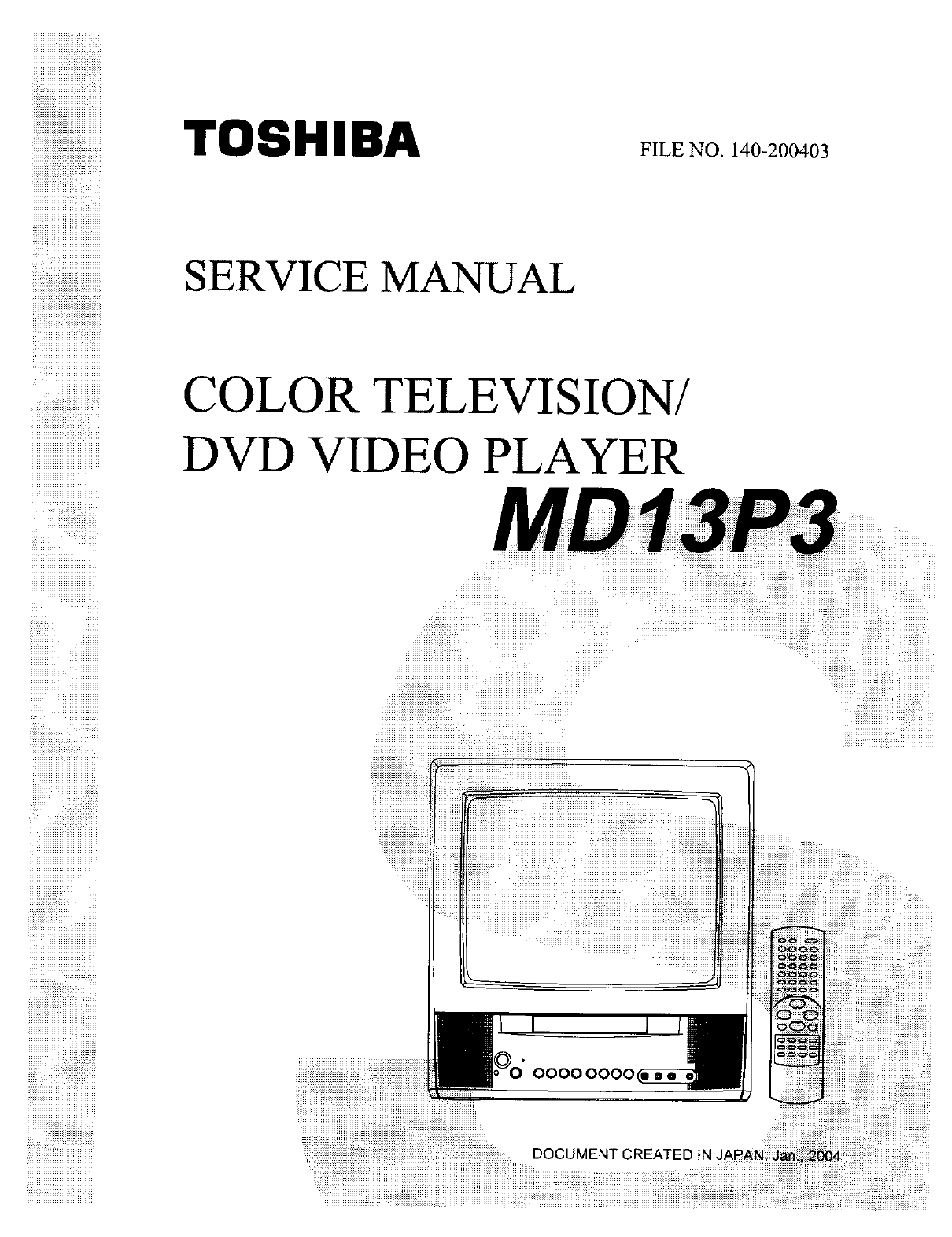
ii_ii_iiiiiiiii_iiiiiii_iii_iii_i_i.... TOSHIBA FILE NO. 140-200403
v
iiii_i_i_!%iiiiiiiii_iii_ii!il
!!!iiiiiiii_
iiiiiiiiiiiiiiii_i_!!!iii!iiii
?i_iiiiiiiiiiiiilii!!_
SERVICE MANUAL
COLOR TELEVISION/
DVD VIDEO PLAYER
0000 0000_
DOCUMENT CREATED tN J/
iiiiiiiiiiiiii iiii
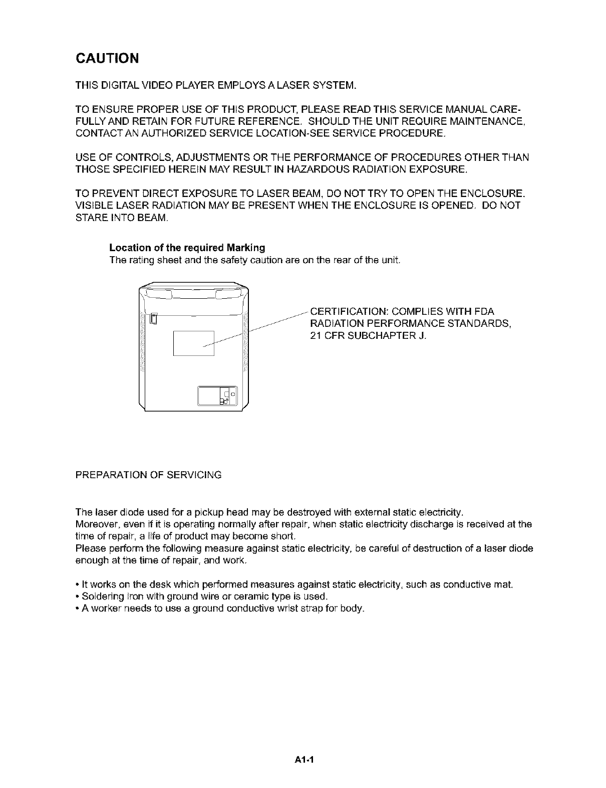
CAUTION
THIS DIGITAL VIDEO PLAYER EMPLOYS A LASER SYSTEM.
TO ENSURE PROPER USE OF THIS PRODUCT, PLEASE READ THIS SERVICE MANUAL CARE-
FULLY AND RETAIN FOR FUTURE REFERENCE. SHOULD THE UNIT REQUIRE MAINTENANCE,
CONTACTAN AUTHORIZED SERVICE LOCATION-SEE SERVICE PROCEDURE.
USE OF CONTROLS, ADJUSTMENTS OR THE PERFORMANCE OF PROCEDURES OTHER THAN
THOSE SPECIFIED HEREIN MAY RESULT IN HAZARDOUS RADIATION EXPOSURE.
TO PREVENT DIRECT EXPOSURE TO LASER BEAM, DO NOT TRY TO OPEN THE ENCLOSURE.
VISIBLE LASER RADIATION MAY BE PRESENT WHEN THE ENCLOSURE IS OPENED. DO NOT
STARE INTO BEAM.
Location of the required Marking
The rating sheet and the safety caution are on the rear of the unit.
CERTIFICATION: COMPLIES WITH FDA
j_ RADIATION PERFORMANCE STANDARDS,
21 CFR SUBCHAPTER J.
PREPARATION OF SERVICING
The laser diode used for a pickup head may be destroyed with external static electricity.
Moreover, even if it is operating normally after repair, when static electricity discharge is received at the
time of repair, a life of product may become short.
Please perform the following measure against static electricity, be careful of destruction of a laser diode
enough at the time of repair, and work.
• It works on the desk which performed measures against static electricity, such as conductive mat.
• Soldering iron with ground wire or ceramic type is used.
• A worker needs to use a ground conductive wrist strap for body.
A1-1
SERVICING NOTICES ON CHECKING
1. KEEP THE NOTICES
As for the places which need special attentions,
they are indicated with the labels or seals on the
cabinet, chassis and parts. Make sure to keep the
indications and notices in the operation manual.
2, AVOID AN ELECTRIC SHOCK
There is a high voltage part inside. Avoid an
electric shock while the electric current is
flowing.
3. USE THE DESIGNATED PARTS
The parts in this equipment have the specific
characters of incombustibility and withstand
voltage for safety. Therefore, the part which is
replaced should be used the part which has
the same character.
Especially as to the important parts for safety
which is indicated in the circuit diagram or the
table of parts as a Z_ mark, the designated
parts must be used.
4. PUT PARTS AND WIRES IN THE
ORIGINAL POSITION AFTER
ASSEMBLING OR WIRING
There are parts which use the insulation
material such as a tube or tape for safety, or
which are assembled in the condition that
these do not contact with the printed board.
The inside wiring is designed not to get closer
to the pyrogenic parts and high voltage parts.
Therefore, put these parts in the original
positions.
5. TAKE CARE TO DEAL WITH THE
CATHODE-RAY TUBE
In the condition that an explosion-proof cathode-
ray tube is set in this equipment, safety is
secured against implosion. However, when
removing it or serving from backward, it is
dangerous to give a shock. Take enough care to
deal with it.
6, AVOID AN X-I_Y
Safety is secured against an X-ray by consider-
ing about the cathode-ray tube and the high
voltage peripheral circuit, etc.
Therefore, when repairing the high voltage pe-
ripheral circuit, use the designated parts and
make sure not modify the circuit.
Repairing except indicates causes rising of high
voltage, and it emits an X-ray from the cathode-
ray tube.
7. PERFORM A SAFETY CHECK AFTER
SERVICING
Confirm that the screws, parts and wiring which
were removed in order to service are put in the
original positions, or whether there are the
portions which are deteriorated around the
serviced places serviced or not. Check the
insulation between the antenna terminal or
external metal and the AC cord plug blades.
And be sure the safety of that.
(INSULATION CHECK PROCEDURE)
1. Unplug the plug from the AC outlet.
2. Remove the antenna terminal on TV and turn
on the TV.
3. Insulation resistance between the cord plug
terminals and the eternal exposure metal
[Note 2] should be more than 1M ohm by
using the 500V insulation resistance meter
[Note 1],
4. If the insulation resistance is less than 1M
ohm, the inspection repair should be
required.
[Note 1]
If you have not the 500V insulation
resistance meter, use a Tester.
[Note 2[
External exposure metal: Antenna terminal
HOW TO ORDER PARTS
Please include the following informations when you order parts. (Particularly the VERSION LETTER.)
1. MODEL NUMBER and VERSION LETTER
The MODEL NUMBER can be found on the back of each product and the VERSION LETTER can be
found at the end of the SERIAL NUMBER.
2. PART NO. and DESCRIPTION
You can find it in your SERVICE MANUAL.
A1-2

IMPORTANT SAFEGUARDS
1. READ INSTRUCTIONS
All the safety and operating instructions should be read before the unit is operated.
2. RETAIN INSTRUCTIONS
The safety and operating instructions should be retained for future reference.
3. HEED WARNINGS
All warnings on the unit and in the operating instructions should be adhered to.
4. FOLLOW INSTRUCTIONS
All operating and use instructions should be followed.
5. CLEANING
Unplug this unit from the wall outlet before cleaning. Do not use liquid cleaners or aerosol cleaners. Use a damp
cloth for cleaning.
6. ATTACHMENTS
Do not use attachments not recommended by the unit's manufacturer as they may cause hazards.
7. WATER AND MOISTURE
Do not use this unit near water. For example, near a bathtub, washbowl, kitchen sink, or laundry tub, in a wet
basement, or near a swimming pool. PORTABLECART WARNING
8. ACCESSORIES (symbol providedby RETAC)
DO not place this unit on an unstable cart, stand, tripod, bracket, or table. The
unit may fall, causing serious injury, and serious damage to the unit. Use only
with a cart, stand, tripod, bracket, or table recommended by the manufacturer.
8A. An appliance and cart combination should be moved with care. Quick stops,
excessive force, and uneven surfaces may cause the appliance and cart
combination to overturn.
9. VENTILATION $3125A
Slots and openings in the cabinet and in the back or bottom are provided for ventilation, to ensure reliable
operation of the unit, and to protect it from overheating. These openings must not be blocked or covered. The
openings should never be blocked by placing the unit on a bed, sofa, rug, or other similar surface. This unit
should never be placed near or over a radiator or heat source. This unit should not be placed in a built-in
installation such as a bookcase or rack unless proper ventilation is provided or the manufacturer's instructions
have been adhered to.
10. POWER SOURCES
This unit should be operated only from the type of power source indicated on the rating plate. If you are not sure
of the type of power supply to your home, consult your appliance dealer or local power company. For units
intended to operate from battery power, or other sources, refer to the operating instructions.
11. GROUNDING OR POLARIZATION
This unit is equipped with a polarized alternating-current line plug (a plug having one blade wider than the other).
This plug will fit into the power outlet only one way. This is a safety feature. If you are unable to insert the plug
fully into the outlet, try reversing the plug. If the plug should still fail to fit, contact your electrician to replace your
obsolete outlet. Do not defeat the safety purpose of the polarized plug. If your unit is equipped with a 3-wire
grounding-type plug, a plug having a third (grounding) pin, this plug will only fit into a grounding-type power
outlet. This too, is a safety feature. If you are unable to insert the plug into the outlet, contact your electrician to
replace your obsolete outlet. Do not defeat the safety purpose of the grounding-type plug.
12. POWER-CORD PROTECTION
Power-supply cords should be routed so that they are not likely to be walked on or pinched by items placed upon
or against them, paying particular attention to cords at plugs, convenience receptacles, and the point where they
exit from the appliance.
13. LIGHTNING
To protect your unit from a lightning storm, or when it is left unattended and unused for long periods of time,
unplug it from the wall outlet and disconnect the antenna or cable system. This will prevent damage to the unit
due to lightning and power line surges.
14. POWER LINES
An outside antenna system should not be located in the vicinity of overhead power lines or other electric light or
power circuits, or where it can fall into such power lines or circuits. When installing an outside antenna system,
extreme care should be taken to keep from touching such power lines or circuits, as contact with them might be
fatal,
15. OVERLOADING
Do not overload wall outlets and extension cords, as this can result in a risk of fire or electric shock.
16. OBJECT AND LIQUID ENTRY
Do not push objects through any openings in this unit, as they may touch dangerous voltage points or short out
parts that could result in fire or electric shock. Never spill or spray any type of liquid into the unit.
A1-3

IMPORTANT SAFEGUARDS (CONTINUED)
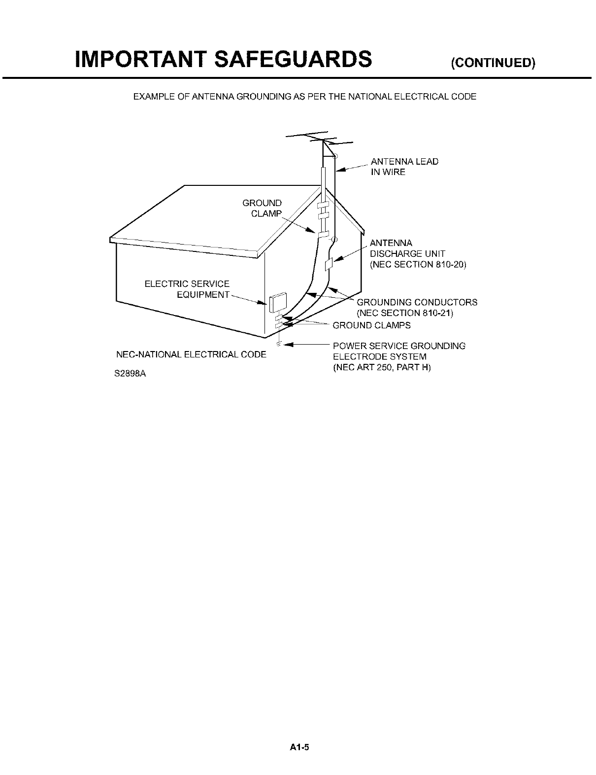
17. OUTDOOR ANTENNA GROUNDING
If an outside antenna or cable system is connected to the unit, be sure the antenna or cable system is grounded
so as to provide some protection against voltage surges and buifi-up static charges. Section 810 of the National
Electrical Code, ANSItNFPA 70, provides information with respect to proper grounding of the mast and supporting
structure, grounding of the lead-in wire to an antenna discharge unit, size of grounding conductors, location of
antenna discharge unit, connection to grounding electrodes, and requirements for the grounding electrode.
18. SERVICING
Do not attempt to service this unit yourself as opening or removing covers may expose you to dangerous voltage
or other hazards. Refer all servicing to qualified service personnel.
19. DAMAGE REQUIRING SERVICE
Unplug this unit from the wall outlet and refer servicing to qualified service personnel under the following
conditions:
a. When the power-supply cord or plug is damaged.
b. If liquid has been spilled, or objects have fallen into the unit.
c. If the unit has been exposed to rain or water.
d. If the unit does not operate normally by following the operating instructions. Adjust only those controls that
are covered by the operating instructions, as an improper adjustment of other controls may result in
damage and will often require extensive work by a qualified technician to restore the unit to its normal
operation.
e. If the unit has been dropped or the cabinet has been damaged.
f. When the unit exhibits a distinct change in porformance, this indicates a need for service.
20. REPLACEMENT PARTS
When replacement parts are required, be sure the service technician uses replacement parts specified by the
manufacturer or those that have the same characteristics as the original parts.
Unauthorized substitutions may result in fire, electric shock or other hazards.
21. SAFETY CHECK
Upon completion of any service or repairs to this unit, ask the service technician to perform safety checks to
determine that the unit is in proper operating condition.
22. WALL OR CEILING MOUNTING
The product should be mounted to a wall or ceiling only as recommended by the manufacturer.
23. HEAT
The product should be situated away from heat sources such as radiators, heat registers, stoves, or other
products (including amplifiers) that produce heat.
24. DISC TRAY
Keep your fingers well clear of the disc tray as it is closing. It may cause serious personal injury.
25. CONNECTING
When you connect the product to other equipment, turn off the power and unplug all of the equipment from the
wall outlet. Failure to do so may cause an electric shock and serious personal injury. Read the owner's manual of
the other equipment carefully and follow the instructions when making any connections.
26. SOUND VOLUME
Reduce the volume to the minimum level before you turn on the product. Otherwise, sudden high volume sound
may cause hearing or speaker damage.
27. SOUND DISTORTION
Do not allow the product output distorted sound for a Iongtime. It may cause speaker overheating and fire.
28. HEADPHONES
When you use the headphones, keep the volume at a moderate level. If you use the headphones continuously
with high volume sound, it may cause hearing damage.
29. LASER BEAM
Do not look into the opening of the disc tray or ventilation opening of the product to see the source of the laser
beam. it may cause sight damage.
30. DISC
Do not use a cracked, deformed, or repaired disc. These discs are easily broken and may cause serious
personal injury and product malfunction.
31. NOTE TO CATV SYSTEM INSTALLER
This reminder is provided to call the CATV system installer's attention to Article 820-40 of the NEC that provides
guidelines for proper grounding and, in particular, specifies that the cable ground shall be connected to the
grounding system of the building, as close to the point of cable entry as practical.
A1-4
IMPORTANT SAFEGUARDS (CONTINUED)
EXAMPLE OF ANTENNA GROUNDING AS PER THE NATIONAL ELECTRICAL CODE
ANTENNA LEAD
IN WIRE
GROUND
CLAMP
ELECTRIC SERVICE
EQL
NEC-NATIONAL ELECTRICAL CODE
$2898A
ANTENNA
JNIT
(NEC SECTION 810-20)
GROUNDING CONDUCTORS
(NEC SECTION 810-21)
GROUND CLAMPS
POWER SERVICE GROUNDING
ELECTRODE SYSTEM
(NEC ART 250, PART H)
A1-5
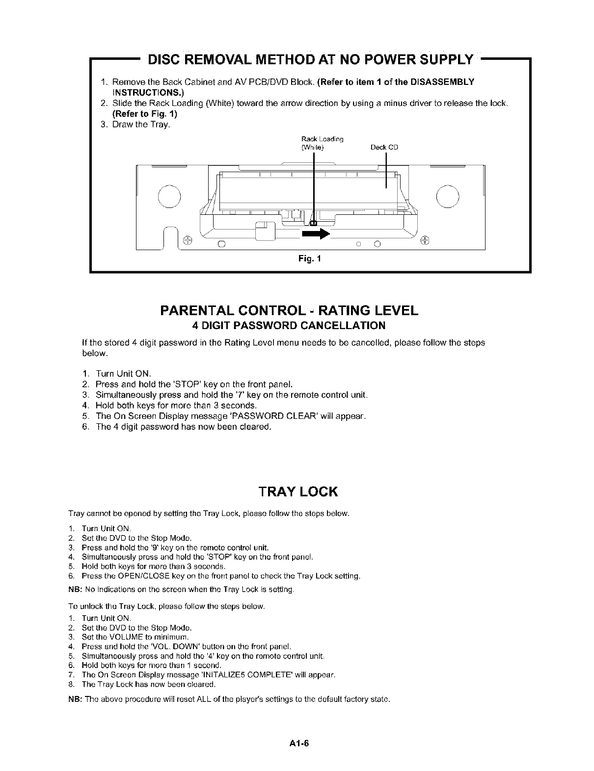
DISC REMOVAL METHOD AT NO POWER SUPPLY
1, Remove the Back Cabinet and AV PCBiDVD Block, (Refer to item 1 of the DISASSEMBLY
iNSTRUCTIONS.)
2, Slide the Rack Loading (White) toward the arrow direction by using a minus driver to release the lock,
(Refer to Fig. 1)
3, Draw the Tray.
Rack Loading
(White) Deck CD
I I I I I I
L_ I
© o o
Fig. 1
PARENTAL CONTROL - RATING LEVEL
4 DIGIT PASSWORD CANCELLATION
If the stored 4 digit password in the Rating Leve] menu needs to be cancelled, please follow the steps
below,
1, Turn Unit ON,
2, Press and hold the 'STOP' key on the front panel.
3. Simultaneously press and hold the '7' key on the remote control unit,
4. Hold both keys for more than 3 seconds.
5. The On Screen Display message 'PASSWORD CLEAR' will appear,
6, The 4 digit password has now been cleared.
TRAY LOCK
Tray cannot be opened by setting the Tray Lock, please follow the steps below,
I. Turn Unit ON.
2. Set the DVD to the Stop Mode.
3. Press and hold the '9' key on the remote control unit.
4, Simultaneously press and hold the 'STOP' key on the front panel
5. Hold both keys for more than 3 seconds.
6. Press the OPEN/CLOSE key on the front panel to cheek the Tray Lock setting.
NB: No #_dications on the screen when the Tray Lock is setting,
To unlock the Tray Lock, please fellow the steps below.
I. Turn Unit ON.
2. Sot the DVD to the Stop Mode.
3. Set the VOLUME to minimum.
4. Press and hold the 'VOL DOWN' button on the front panel
5, Simultaneously press and hold the '4' key on the remote control unit.
6. Hold both keys for more than 1 second.
7. The On Screen Display message 'INITALIZE5 COMPLETE' will appear.
8. The Tray Lock has now been cleared.
NB: The above procedure wilt reset ALL of the player s settings to the default factory state.
AI-6
TABLE OF CONTENTS
CAUTION ............................................................................................................................ A!-!
SERVICING NOTICES ON CHECKING ..................................................................................... A!-2
HOWTO ORDER PARTS .......................................................................................................... A!-2
IMPORTANT SAFEGUARDS ..................................................................................................... A1-3~A!-5
DISC REMOVAL METHOD AT NO POWER SUPPLY ............................................................. A!-6
PARENTAL CONTROL*RATING LEVEL .................................................................................. A!-6
TRAY LOCK ................................................................................................................................ A!-6
TABLE OF CONTENTS .............................................................................................................. A2-1
GENERAL SPECIFICATIONS ................................................................................................... A3-! ~A3-6
DISASSEMBLY INSTRUCTIONS
1. REMOVAL OF MECHANICAL PARTS AND P. C. BOARDS ............................................ B1-!, B!-2
2, REMOVAL OF DVD DECK PARTS ................................................................................... B2-1~B2-4
3. REMOVAL OF ANODE CAP .............................................................................................. B3-!
4. REMOVAL AND INSTALLATION OF FLAT PACKAGE IC ............................................... B4-!, B4_2
SERVICE MODE LIST ................................................................................................................ C-1
CONFIRMATION OF HOURS USED ......................................................................................... C-1
WHEN REPLACING EEPROM (MEMORY) IC .......................................................................... C-2
ELECTRICAL ADJUSTMENTS .................................................................................................. D-I~D-6
BLOCK DIAGRAMS
DVD .......................................................................................................................................... E-l, E-2
TV ............................................................................................................................................ E-3, E-4
POWER .................................................................................................................................. E-5, E-6
PRINTED CIRCUIT BOARDS
DVD .......................................................................................................................................... F-l, F-2
AV/CRT .................................................................................................................................... F-3~F-6
RELAY/SW .............................................................................................................................. F*7, F-8
SCHEMATIC DIAGRAMS
MPEG/MtCON ......................................................................................................................... G-l, G-2
MEMORY ................................................................................................................................. G-3, G-4
RF AMP/DSP ........................................................................................................................... G-5, G-6
AUDIO/VIDEO ......................................................................................................................... G-7, G-8
REGULATOR ........................................................................................................................... G-9, G-10
MtCON/TUNER ....................................................................................................................... G-!1, G-12
VIF/StF/CHROMA .................................................................................................................... G-13, G-14
SOUND AMP ........................................................................................................................... G-15, G-16
IN/OUT ..................................................................................................................................... G-17, G-18
STEREO .................................................................................................................................. G-!9, G-20
DEFLECTION .......................................................................................................................... G-2!, G-22
CRT .......................................................................................................................................... G-23, G-24
POWER ................................................................................................................................... G-25, G-26
RELAY/SW/FG ........................................................................................................................ G-27, G-28
INTERCONNECTIGN DIAGRAM ............................................................................................... G-29, G-30
WAVEFORMS ............................................................................................................................. H-I~H-3
MECHANICAL EXPLODED VIEWS ........................................................................................... t1-!~I1-3
DVD DECK EXPLODED VIEW ................................................................................................... t2-!
MECHANICAL REPLACEMENT PARTS LIST ......................................................................... J1-1
DVD DECK PLACEMENT PARTS LIST .................................................................................... J2-1
ELECTRICAL REPLACEMENT PARTS LIST ........................................................................... J3-1~J3-5
A2-1
GENERAL SPECIFICATIONS
G-t IV CRT CRT Size iVisual Size
System CRT Type
Deflection
Magnetic Field BViBH
Color System
Speaker
Position
Size
Impedance
Sound Output Max
t0%(Typical)
G-2 DVD System Color System
Disc
Disc Diameter I
Deck Disc Loading Systarq
Motor
Pick up
Playback time(Max) DVD 1-Layer
DVD 2-Layer
CD
Video CD
Search speed Fwd
Slow speed
G-3 [unlng Broadcasting System
System Tuner and
Receive CH
Intat rqediata
Frequency
Preset CH
Stereo/Dual TV Sound
Tuner Sound Muting
G-4 Signal Video Signal
RGB Signal
Audio Signal
Rev
Systarq
Destination
Tuning System
Input Impedance
CH Coverage
Picture(PP)
Sound(FS)
FP-FS
Input Level
Output Level
SiN Ratio (Weighted)
Horizontal Resolution at DVD Mode
Output Level
Input Level
Output Level
Digital Output Level
SiN Ratio at DVD (Weighted)
Harmonic Distortion
Frequency Response :
Actual
Actual
Actual
Actual
DVD
_VideoCD
SVCD
at CD
t3inch i335.4 mmV
Normal
90 degree
+045G /0.18G
NTSC
2 Speaker
Front
t .5 x 2.7 inch
8 ohm
t.5W + 1.5W
t.OW + 1.0W
NTSC
DVD_ CD-DA, CD_PJRW, Video CD
120 mm, 80 mm
Front Loading
2 Motors
t-Lens 2-Beams System
t35min (4.7GB)
245rain (8.5GB)
74min
74min
2-20 times /4 step
2_45 times {DVD, VIDEO CD)
4_40 times (CD)
2-20 times /4 step
2_45 times {DVD, VIDEO CD)
4_40 times (CD)
Fwd ti7 - 1i2 times
Rev 1/7 - 1i2 times
US System M
tTuner
US(wlCATV)
F-Synth
VHFiURF 75 Ohm
2~69, 4A, A-5~A-1, A~I, J~W, W+l ~W+84
45 75MHz
4t 25MHz
4 50MHz
No
US-Stereo
Yes
tVI_pi75 ohm
-8 OdBmi5Ok ohm
0.5 V p-p/75 ohm
G-5 Power Power Source AC t2OV, 60Hz
DC
Power Consumption at AC 75W at t2OV6OHz
at DC
Stand by (at AC) 5W at 120V 60Hz
Per Year _- kWh/Year
Protector Power Fuse Yes
G-6 Regulation Safety UL
Radiation FCC
X-Radiation DHHS
Laser DHHS
G-7 [emperature Operation +5oC ~+40oC
Storage -20oC ~ +6OoC
G-8 Operating Humidity Less than 80% RH
A3-1
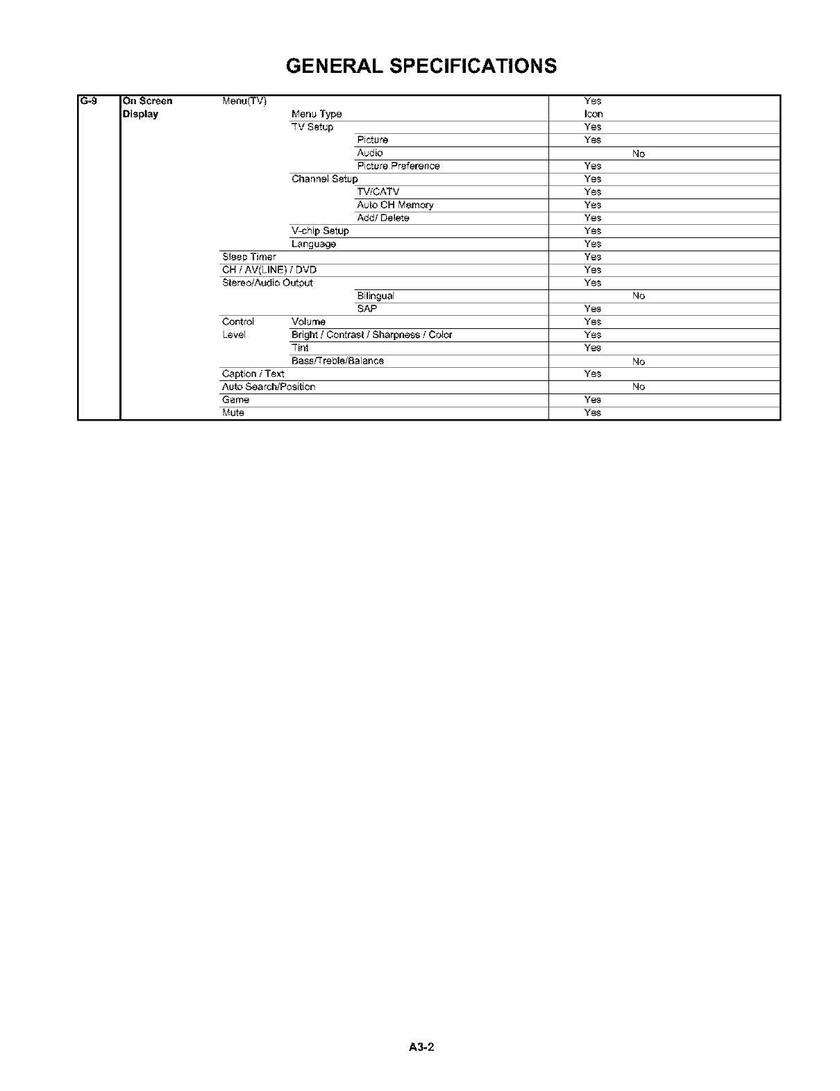
GENERAL SPECIFICATIONS
G-g On Screen MenuffV)
Display Menu Type
TV Setup
Picture
Audio
Bictu_ Preference
Channel SetupTViCATV
Auto CH Memory
Add/Delete
V_chip Setup
Language
Sleep Timer
CH /AV(LINE) iDVD
Stereo/Audio Output
Bilingual
SAP
Control Volume
Level Bright /Contrast iSharpness iColor
Tint
Bass#r rebleiBalance
Caption iText
Auto Search/Position
Game
Mute
Icon
Yes
Yes
No
Yes
Yes
Yes
Yes
Yes
Yes
Yes
Yes
Yes
Yes
No
Yes
Yes
Yes
Yes
No
Yes
No
Yes
Yes
A3-2
GENERAL SPECIFICATIONS
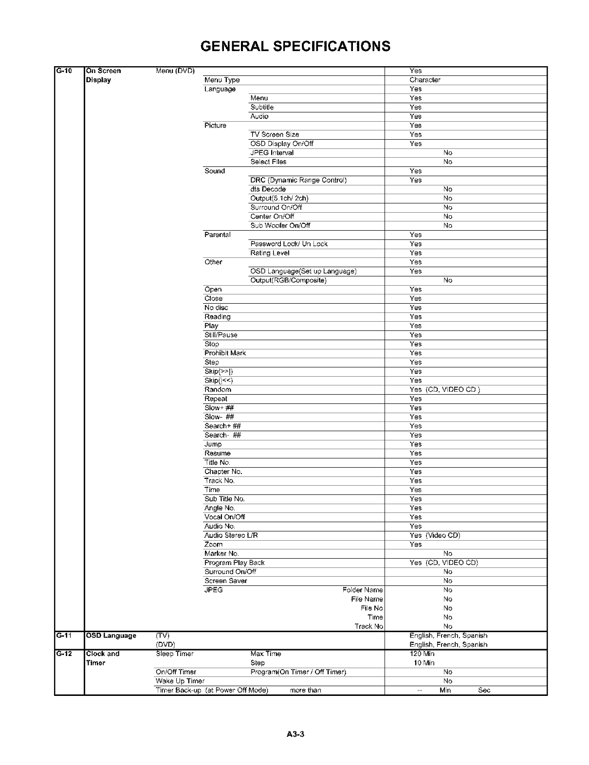
G-10 011 Screen Menu (DVD)
Display MenuType
Language
Picture
Sound
Parental
Other
Menu
SubtitEe
Audio
TV Screen Size
OSD Display On/Off
JPEG Interval
Select Files
DRC (Dynamic Range Control)
dts Decode
Output(5 lchi 2ch)
Surround OniOff
Center On/Off
Sub Woofer On/Off
Password Lock/Un Lock
Rating Level
OSD Language(Set up Language)
Output(RGBiCorqposite)
Open
Close
No disc
Reading
Play
Still/Pause
Stop
Prohibit Mark
Step
Skip(>>l)
Skip(<<)
Random
Repeat
Slow+
Slow-
Search+
Search-
Jump
Resurqe
Title No
Chapter NO.
Track NO
Time
Sub Title No
Angle No.
Vocal OniOff
Audio NO.
Audio Stereo UR
Zoom
Marker NO.
Program Play Back
Surround On/Off
Screen Saver
JPEG Folder Name
File Name
File No
Time
Track NO
G-11 OSD Language (TV)
(DVD)
G-12 Clock and Sleep Timer Max Time
[inter Step
On/Off Timer Program(On Timer /Off Timer)
Wake Up Timer
Timer Back_up (at Power Off Mode) more than
Yes
Character
Yes
Yes
Yes
Yes
Yes
Yes
Yes
No
No
Yes
Yes
No
No
No
No
No
Yes
Yes
Yes
Yes
Yes
No
Yes
Yes
Yes
Yes
Yes
Yes
Yes
Yes
Yes
Yes
Yes
Yes (CD, VIDEO CD )
Yes
Yes
Yes
Yes
Yes
Yes
Yes
Yes
Yes
Yes
Yes
Yes
Yes
Yes
Yes
Yes (Video CD)
Yes
No
Yes (CD, VIDEO CD)
No
No
No
No
No
No
No
English, French, Spanish
English, French, Spanish
120 Min
1OMin
NO
NO
- Min Sec
A3-3
GENERAL SPECIFICATIONS
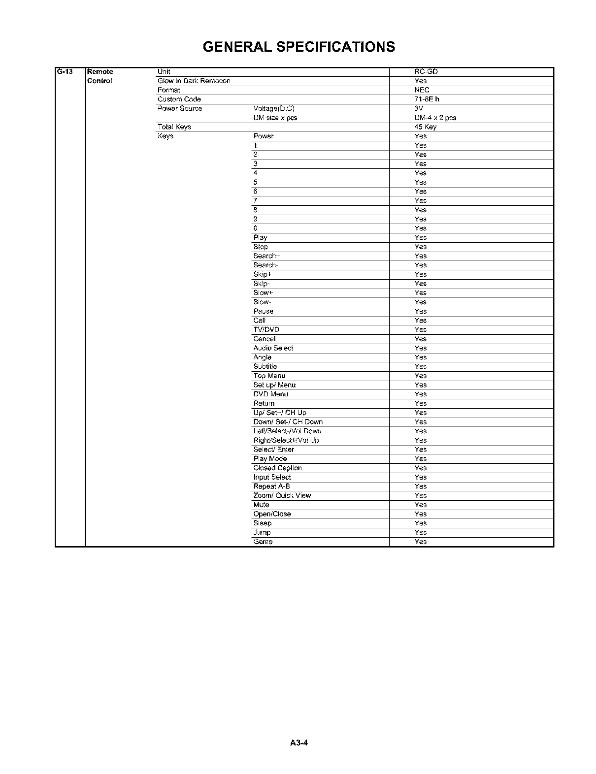
G-13 Remote Unit
Control Glow in Dark Remo-'_on
Format
Custom Code
Power Source Voltage(D.C)
UM size x pus
Total Keys
Keys Power
t
2
3
4
5
6
7
8
g
0
Play
Stop
Search+
Search-
Skip+
Skip-
Slow+
Slow-
Pause
Cal_
TViDVD
Cancel
Audio Select
Angle
Subtitle
Top Menu
Set up/Menu
DVD Menu
Return
Up/Set+i CH Up
Downi Set-/CH Down
Le ftiSelectdVol Down
RightsSelect+/Vol Up
Select s Enter
Play Mode
Closed Caption
Input Select
Repeat A-B
Zoom/Quick View
Mute
OpenlCIose
Sleep
Jump
Game
RC-GD
NEC
7t-8E h
3V
UM_4 x 2 pcs
45 Key
Yes
Yes
Yes
Yes
Yes
Yes
Yes
Yes
Yes
Yes
Yes
Yes
Yes
Yes
Yes
Yes
Yes
A3-4
GENERAL SPECIFICATIONS
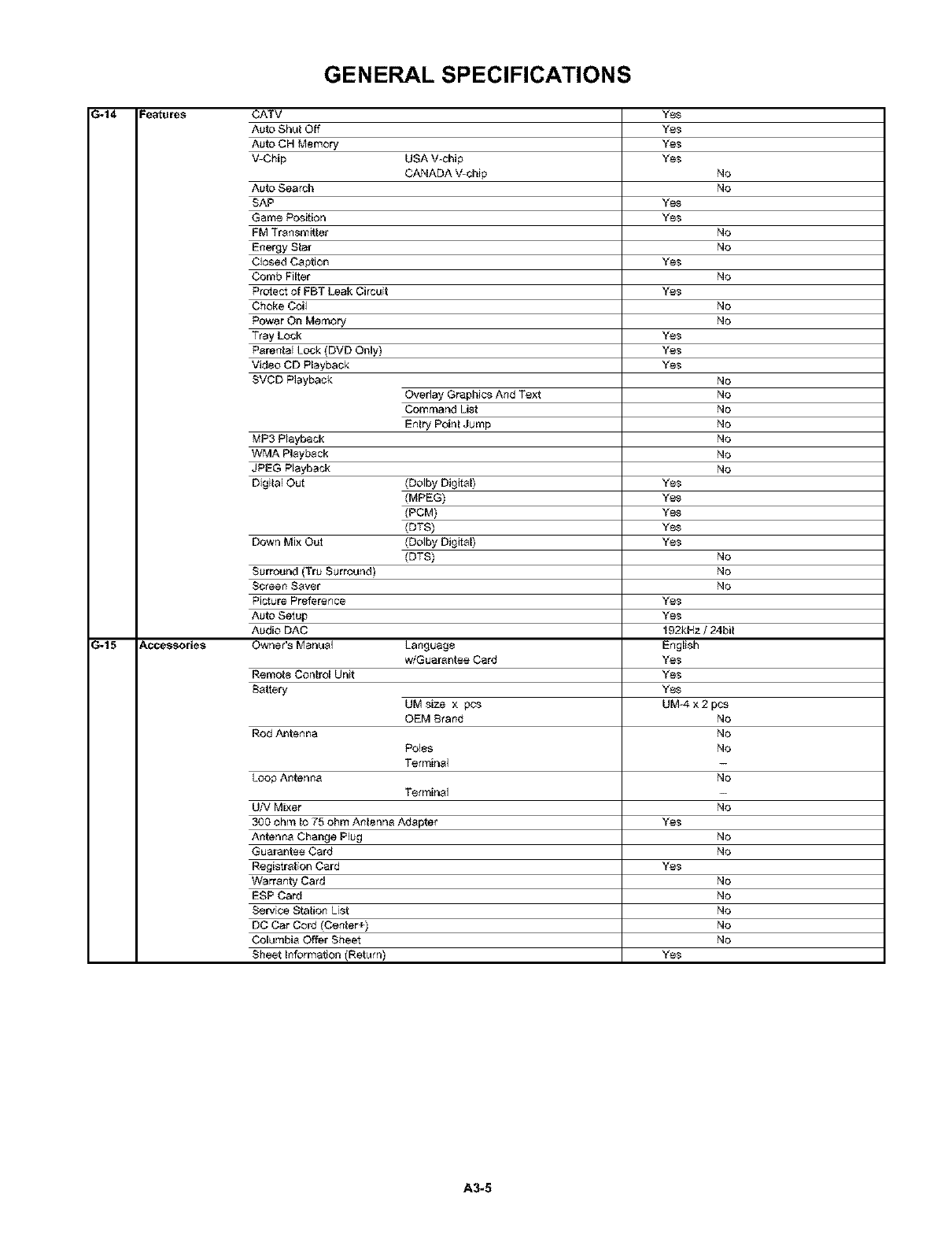
G-14 Features CATV
Auto Shut Off
Auto CH Memory
V-Chip USA V-chip
CANADA V-chip
Auto Search
SAP
Game Position
FM Transmitter
Energy Star
Closed Caption
Comb Filter
P_etestof FBT Leak Circuit
Choke Coil
Power On Memory
Tray Lock
Parental Lock (DVD Only)
Video CD Playback
SVCD Playback
MP3 Playback
WMA Playback
JPEG Playback
Digital Out
Down Mix Out
Overlay Graphics And Text
Command List
Entry Point Jump
(Dolby Digital)
(MPEG)
(PCM)
(DTS)
(Dolby Digital)
(DTS)
Surround (Tru Surround)
Screen Saver
Picture Preference
Auto Setup
Audio DAC
G-15 &ccessories Owner's Manual Language
w/Guarantee Card
Remote Control Unit
Battery
UM size × pcs
OEM Brand
Rod f_ntanna
Poles
Temqinal
Loop Antenna Temqinal
UN Mixer
300 ohm to 75 ohm Antenna Adapter
Antenna Change Plug
Guarantee Card
Registration Card
Warranty Card
ESP Card
Service Station List
DC Car Cord (Center+)
Columbia Offer Sheet
Sheet Information (Return)
Yes
No
No
Yes
No
No
No
No
No
No
No
No
No
No
No
No
Yes
Yes
Yes
No
No
No
tg2kHz /24bit
English
Yes
UM4 x 2 pcs
No
No
No
No
No
No
No
No
No
No
No
No
A3-5
GENERAL SPECIFICATIONS
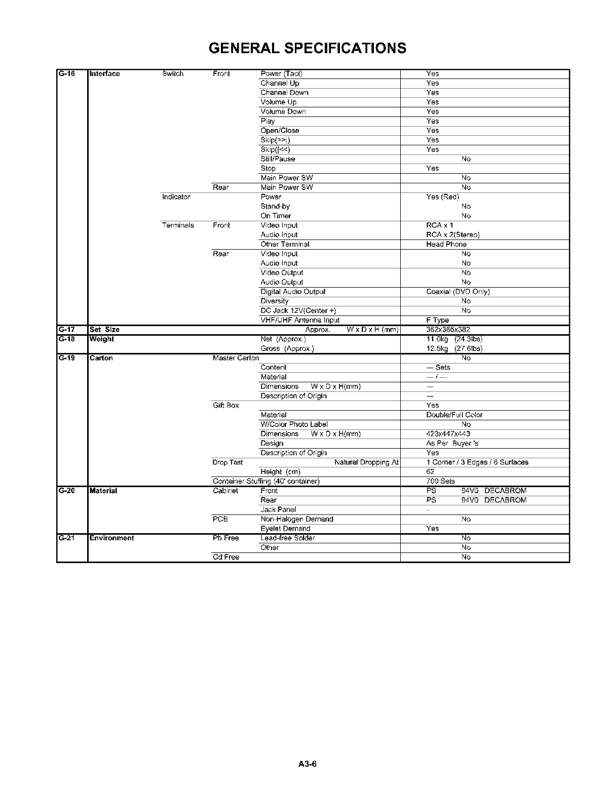
G-16 Interface
G-17 Set Size
G-18 #/eight
G-19 Carton
G-20 Material
G-2t Environment
Switch
Indicator
Terminals
Front Power (Tact)
Channel Up
Channel Down
Volume Up
Volume Down
Piny
Open/Close
Skip(>>)
Skip(l<<)
Still/Pause
Stop
Main Power SW
Rear Main Power SW
Power
Stand-by
On Timer
Front Video input
Audio Input
Other Terminal
Rear Video input
Audio input
Video Output
Audio Output
Digital Audio Output
Diversity
DC Jack t2V(Center +)
VHFiUHF/_tenna input
Approx. W x D x H (ram)
Net (Approx)
Gross (Approx.)
Master Carton
Content
Material
Dimensions W x D x H(mm)
Description of Origin
Gift Box
Material
W/Color Photo Label
Dimensions W x D x H{mr'q)
Design
Description of Origin
Drop Test Natural Dropping At
Height (cm)
Container Stuffing (40' container)
Cabinet Front
Rear
Jack Panel
PCB Non-Halogen Demand
Eyelet Demand
Pb Free Lead4ree Solder
Other
Cd Free
Yes
Yes
Yes
Yes
Yes
Yes
Yes
Yes
Yes
No
Yes
No
No
Yes (Red)
No
No
RCA x 1
RCA x 2(Stereo)
Head Phone
No
No
No
No
Coaxial (DVD Only)
No
No
F Type
362x365x382
tt0kg (24.31bs)
t25kg (27.61bs)
NO
-- Sets
Yes
Double/Full Color
No
423x447x443
As Per Buyer's
Yes
t Corner /3 Edges /6 Surfaces
62
700 Sets
PS 94V0 DECABROM
PS 94V0 DECABROM
No
Yes
No
No
No
A3-6
DISASSEMBLY INSTRUCTIONS
1. REMOVAL OF MECHANICAL PARTS
AND P.C. BOARDS
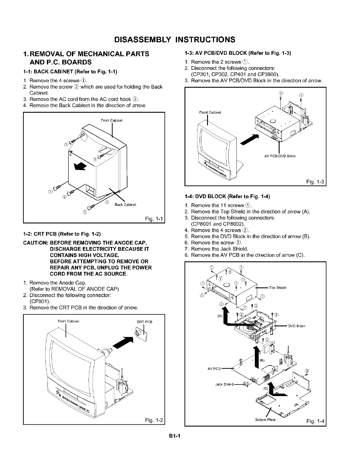
1-1 : BACK CABINET (Refer to Fig. 1-1)
1, Remove the 4 screws ,i),
2, Remove the screw z which are used for holding the Back
Cabinet.
3. Remove the AC cord from the AC cord hook _.
4, Remove the Back Cabinet in the direction of arrow,
Fror_i Cabinei
Fig. 1-1
1-2: CRT PCB (Refer to Fig. 1-2)
CAUTION: BEFORE REMOVING THE ANODE CAP,
DISCHARGE ELECTRICITY BECAUSE IT
CONTAINS HIGH VOLTAGE.
BEFORE ATTEMPTING TO REMOVE OR
REPAIR ANY PCB, UNPLUG THE POWER
CORD FROM THE AC SOURCE.
1, Remove the Anode Cap.
(Refer to REMOVAL OF ANODE CAP)
2, Disconnect the following connector:
(CP801).
3, Remove the CRT PCB in the direction of arrow.
F='or_iCabinei CRT PCB
Fig. 1-2
1-3: AM PCB/DVD BLOCK (Refer to Fig. 1-3)
1. Remove the 2 screws 1i.
2. Disconnect the following connectors:
(CP301, CP302, CP401 and CP3800).
3. Remove the AV PCB/DVD Block in the direction of arrow,
Front Cabinet
AV PCB/_.)VD Block
Fig. 1-3
1-4: DVD BLOCK (Refer to Fig. 1-4)
1. Remove the 11 screws i.
2. Remove the Top Shield in the direction of arrow (A).
3. Disconnect the following connectors:
(CP8001 and CP8002).
4. Remove the 4 screws '_.
5. Remove the DVD Block in the direction of arrow (B).
6. Remove the screw ,_).
7. Remove the Jack Shield.
8. Remove the AV PCB in the direction of arrow (C),
®
_ito,. Pixie Fig. 1-4
B1-1
DISASSEMBLY INSTRUCTIONS
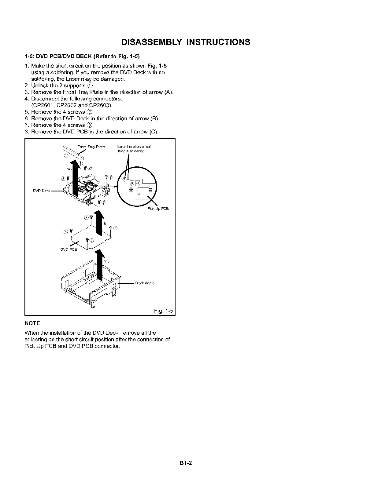
1-5: DVD PCBIDVD DECK (Refer to Fig. 1-5)
1. Make the short circuit on the position as shown Fig. 1-5
using a soldering. If you remove the DVD Deck with no
soldering, the Laser may be damaged.
2. Unlock the 2 supports i),
3. Remove the Front Tray Plate in the direction of arrow (A),
4. Disconnect the following connectors:
(CP2601, CP2602 and CP2603),
5. Remove the 4 screws '2.
6. Remove the DVD Deck in the direction of arrow (B),
7. Remove the 4 screws '_.
8. Remove the DVD PCB in the direction of arrow (C).
Pick Up PCB
Fig. 1-5
NOTE
When the installation of the DVD Deck, remove all the
soldering on the short circuit position after the connection of
Pick Up PCB and DVD PCB connector,
BI-2
DISASSEMBLY INSTRUCTIONS
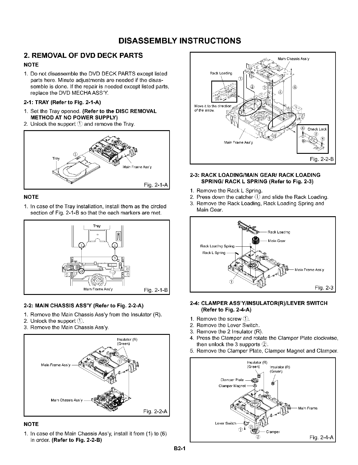
2. REMOVAL OF DVD DECK PARTS
NOTE
1, Do not disassemble the DVD DECK PARTS except listed
parts here, Minute adjustments are needed if the disas-
semble is done. If the repair is needed except listed parts,
replace the DVD MECHAASS'Y,
2-1 : TRAY (Refer to Fig. 2-1-A)
1, Set the Tray opened. (Refer to the DISC REMOVAL
METHOD AT NO POWER SUPPLY)
2, Unlock the support 1 and remove the Tray.
\
Mair_ ran!e Ass'y
Fig. 2-1-A
NOTE
1, In case of the Tray installation, install them as the circled
section of Fig. 2-1-B so that the each markers are met.
Ma;n Chsssis Assy
/
Malr_ ran!e Ass'y
2-3: RACK LOADINGIMAIN GEAR/RACK LOADING
SPRING! RACK L SPRING (Refer to Fig. 2-3)
1. Remove the Rack L Spring.
2. Press down the catcher [! and slide the Rack Loading.
3. Remove the Rack Loading, Rack Loading Spring and
Main Gear.
ManF,ameAss'y Fig. 2-1-B
2-2: MAIN CHASSIS ASS'Y (Refer to Fig. 2-2-A)
1, Remove the Main Chassis Ass'y from the insulator (R),
2, Unlock the support 1,
3, Remove the Main Chassis Ass'y.
{nsulator(R)
Fig. 2-2-A
NOTE
1, In case of the Main Chassis Ass'y, install it from (1) to (6)
in order. (Refer to Fig. 2-2-B)
Y
/
Fig. 213
2-4: CLAMPER ASS'Y!INSULATOR(R)ILEVER SWITCH
(Refer to Fig. 2.4_A)
1. Remove the screw 1.
2. Remove the Lever Switch.
3. Remove the 2 Insulator (R).
4. Press the Clamper and rotate the Clamper Plate clockwise,
then unlock the 3 supports 2.
5. Remove the Clamper Plate, Clamper Magnet and Clamper.
B2-1
Fig. 2-4-A
DISASSEMBLY INSTRUCTIONS
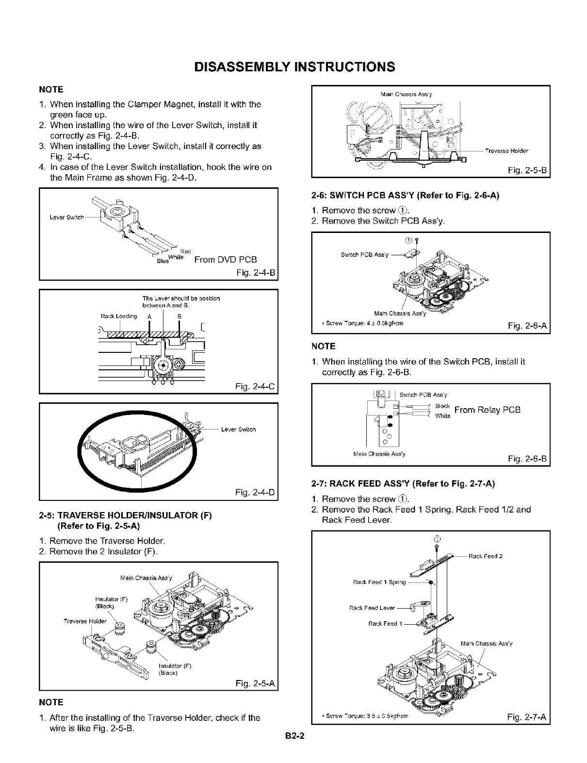
NOTE
1. When installing the Clamper Magnet, install it with the
green face up.
2. When installing the wire of the Lever Switch, install it
correctly as Fig. 2-4-B.
3. When installing the Lever Switch, install it correctly as
Fig. 2-4-C.
4. In case of the Lever Switch installation, hook the wire on
the Main Frame as shown Fig. 2-4-D.
Main Chassis Ass'y
The ke,,e slsoLId be ;Josiiion
b_tweelt A 8itd S.
Rack Loadir_g A B
Fig. 2-4-C
2-5: TRAVERSE HOLDER!INSULATOR (F)
(Refer to Fig. 2-5-A)
1, Remove the Traverse Holder.
2, Remove the 2 Insulator (F),
Fig. 2-4-D
Insulator (F)
(BIBck)
Tl'_Vel Be Holder
Insulator (F)
(Back)
Fig. 2-5-A
NOTE
1. After the installing of the Traverse Holder, check if the
wire is like Fig. 2-5-B. B2-2
2-6: SWITCH PCB ASS3" (Refer to Fig. 2-6-A)
1. Remove the screw ,i!.
2. Remove the Switch PCB Ass'y.
Fig. 2-6-A
NOTE
1. When installing the wire of the Switch PCB, install it
correctly as Fig. 2-6-B.
© Swiich PCB Ass'y
,__ slack From Relay PCB
While
FSailt Chassis Ass'y Fig. 2-6-B
2-7: RACK FEED ASS3' (Refer to Fig. 2-7-A)
1. Remove the screw ,i!.
2. Remove the Rack Feed 1 Spring, Rack Feed 1/2 and
Rack Feed Lever.
@
Rack Feed 1
Ma;n Chassis Ass'y
Fig. 2-7-A
DISASSEMBLY INSTRUCTIONS
NOTE
1, After the assembly of the Rack Feed, check if the Rack
Feed 1/2 is moving smoothly. (Refer to Fig. 2-7-B)
2, In case of the Rack Feed Ass'y installation, install cor-
rectly as Fig. 2-7-C,
Moving smoothly Fig. 2-7-B
2-8: RELAY PCB ASS'Y (Refer to Fig. 2-8-A)
1, Remove the screw ,it,
2, Remove the Relay PCB Ass'y.
• Screw Torque: 4 ± O 5kgf,cm !") Fig. 2-8-A
NOTE
1, When installing the wire of the Relay PCB, install it
correctly as Fig. 2-8-B,
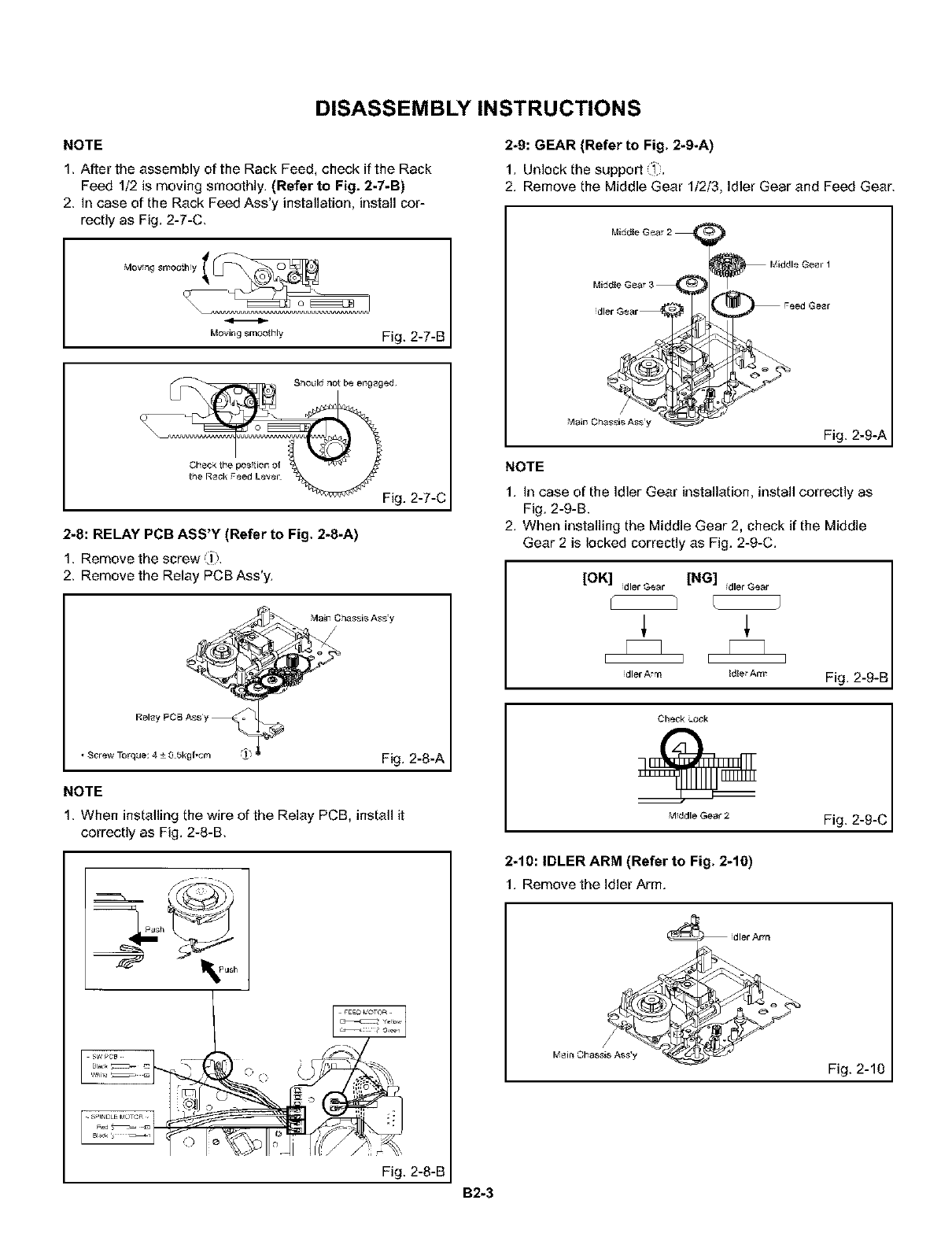
2-9: GEAR (Refer to Fig. 2-9-A)
1. Un ock the support
2. Remove the Middle Gear 1/2/3, Idler Gear and Feed Gear,
Middle Gear 2
M_ddle Gear 3 4
dler Gear
Malr_ Ch_
Fig. 2-9-A
NOTE
1. In case of the Idler Gear installation, install correctly as
Fig. 2-9-B.
2. When installing the Middle Gear 2, check if the Middle
Gear 2 is locked correctly as Fig. 2-9-C.
[OK] dietGear [NG] dietGear
[- "] I
diet Arm Idle An1! Fig. 2-9-B
Check LOCk
Mddle Gear2 Fig. 2-9-C
2-10: IDLER ARM (Refer to Fig. 2-10)
1. Remove the Idler Arm.
_ush
FEE0 _,_OTOR.
Fig. 2-8-B
idler Arm
B2-3
Fig. 2-10
DISASSEMBLY INSTRUCTIONS
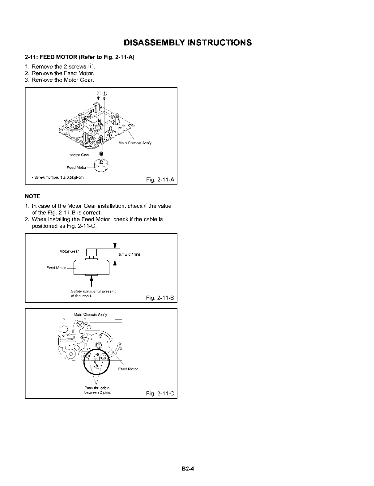
2-11: FEED MOTOR (Refer to Fig. 2-11-A)
1, Remove the 2 screws _i),
2, Remove the Feed Motor.
3, Remove the Motor Gear,
• _¢rew Torque; 1_ 0 bl{gf,cm Fig. 2-11-A
NOTE
1, In case of the Motor Gear installation, check if the value
of the Fig. 2-11-B is correct.
2, When installing the Feed Motor, check if the cable is
positioned as Fig. 2-11-C,
Motor__(Gear 6 £0 rnrn
Safety $L_rface for _ressirl_
of tbe ir!sei_, Fig. 2-11 -B
Mair_ Chassis Ass'y
Pass the cable
be[ween 2 prls. Fig. 2-11 -C
B2-4
DISASSEMBLY INSTRUCTIONS
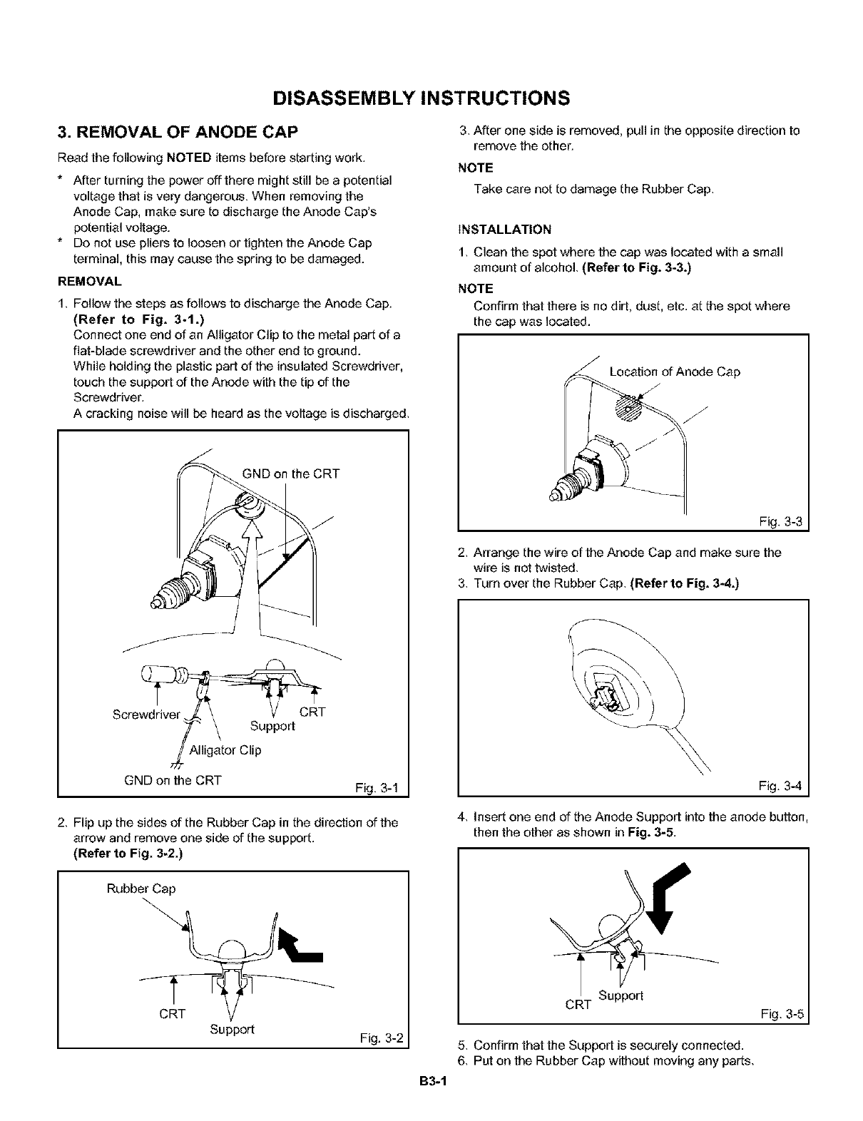
3. REMOVALOFANODECAP
Read the following NOTED items before starting work.
*After turning the power off there might still be a potential
voltage that is very dangerous. When removing the
Anode Cap, make sure to discharge the Anode Cap's
potential voltage.
Do not use pliers to loosen or tighten the Anode Cap
terminal, this may cause the spring to be damaged.
REMOVAL
1, Follow the steps as follows to discharge the Anode Cap.
(Refer to Fig. 3-1.)
Connect one end of an Alligator Clip to the metal part of a
fiat-blade screwdriver and the other end to ground.
While holding the plastic part of the insulated Screwdriver,
touch the support of the Anode with the tip of the
Screwdriver.
A cracking noise will be heard as the voltage is discharged,
J
GND on the CRT
J
j7 f _
)
Sore f \ Support
,,_/Alligator Clip
GND on the CRT Fig. 3-1
2, Flip up the sides of the Rubber Cap in the direction of the
arrow and remove one side of the support.
(Refer to Fig. 3-2.)
3, After one side is removed, pull in the opposite direction to
remove the other.
NOTE
Take care not to damage the Rubber Cap,
INSTALLATION
1, Clean the spot where the cap was located with a small
amount of alcohol, (Refer to Fig. 3-3.)
NOTE
Confirm that there is no dirt, dust, etc. at the spot where
the cap was located.
Location of Anode Cap
J
2, Arrange the wire of the Anode Cap and make sure the
wire is not twisted,
3, Turn over the Rubber Cap, (Refer to Fig. 3-4.)
Fig. 3-4
4, Insert one end of the Anode Support into the anode button,
then the other as shown in Fig. 3-5.
Rubber Cap
CRT
Support Fig. 3-2
Fig. 3-5
5, Confirm that the Support is securely connected.
6, Put on the Rubber Cap without moving any parts,
B3-1
DISASSEMBLY INSTRUCTIONS
4. REMOVAL AND INSTALLATION OF FLAT
PACKAGE IC
REMOVAL
1. Put the Masking Tape (cotton tape) around the Fiat
Package IC to protect other parts from any damage,
(Refer to Fig, 4-1,)
NOTE
Masking is carried out on all the parts located within
10 mm distance from IC leads.
IC
Masking Tape
(cotton Tape)
Fig. 4-1
2. Heat the IC leads using a blower type IC desoldering
machine. (Refer to Fig. 4-2.)
NOTE
3. When IC starts moving back and forth easily after
desoldering completely, pickup the corner of the IC using
a tweezers and remove the IC by moving with the IC
desoldering machine. (Refer to Fig. 4-3.}
NOTE
Some ICs on the PCB are affixed with glue, so be
careful not to break or damage the foil of each IC
leads or solder lands under the IC when removing it.
Blower type IC
desoldering machine
Tweezers
Fig. 4-3
Do not add the rotating and the back and forth direc-
tions force on the IC, until IC can move back and forth
easily after desoldering the IC leads completely.
Blower type IC
desoldering machine
Fig. 4-2
4. Peel off the Masking Tape.
5. Absorb the solder left on the pattern using the Braided
Shield Wire. (Refer to Fig. 4-4.}
NOTE
Do not move the Braided Shield Wire in the vertical
direction towards the IC pattern.
Braided Shield WAre
Soldering Iron
IC pa_em
Fig. 4-4
B4-1
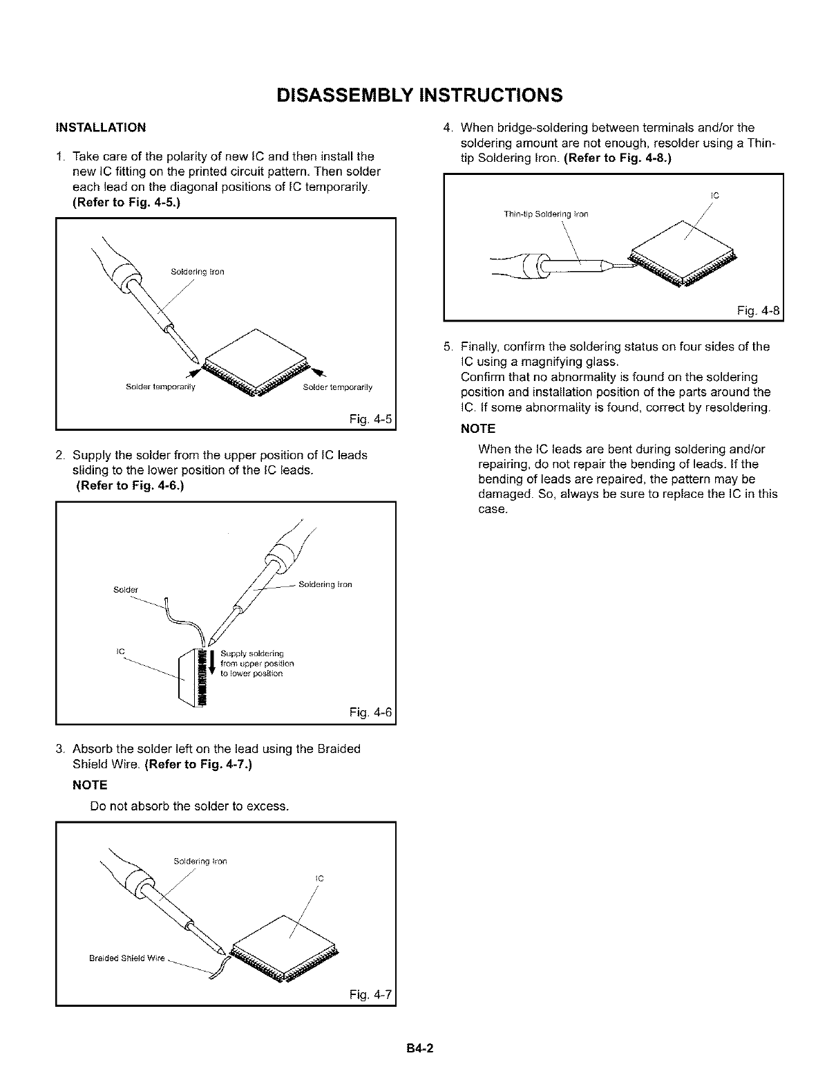
DISASSEMBLY INSTRUCTIONS
INSTALLATION
f. Take care of the polarity of new IC and then install the
new IC fitting on the printed circuit pattern, Then solder
each lead on the diagonal positions of IC temporarily.
(Refer to Fig, 4-5,)
Soldering Iron
/
/
Solder temporarily Solder temporarily
Fig. 4-5
2. Supply the solder from the upper position of IC leads
sliding to the lower position of the IC leads.
(Refer to Fig. 4-6.)
4. When bridge*soldering between terminals and/or the
soldering amount are not enough, resolder using a Thin-
tip Soldering Iron. (Refer to Fig. 4-8.)
_C
Thimtip Sotdedng Iron
Fig. 4-8
5. Finally, confirm the soldering status on four sides of the
IC using a magnifying glass.
Confirm that no abnormality is found on the soldering
position and installation position of the parts around the
IC. If some abnormality is found, correct by resoldering.
NOTE
Solder_% __ooldSoldering Iron
to lower position
Fig. 4-6
When the IC leads are bent during soldering and/or
repairing, do not repair the bending of leads, If the
bending of leads are repaired, the pattern may be
damaged. So, always be sure to replace the IC in this
case.
3. Absorb the solder left on the lead using the Braided
Shield Wire. (Refer to Fig. 4W.)
NOTE
Do not absorb the solder to excess.
Soldering iron
/
Braided Shield Wire
Fig. 4-7
B4-2
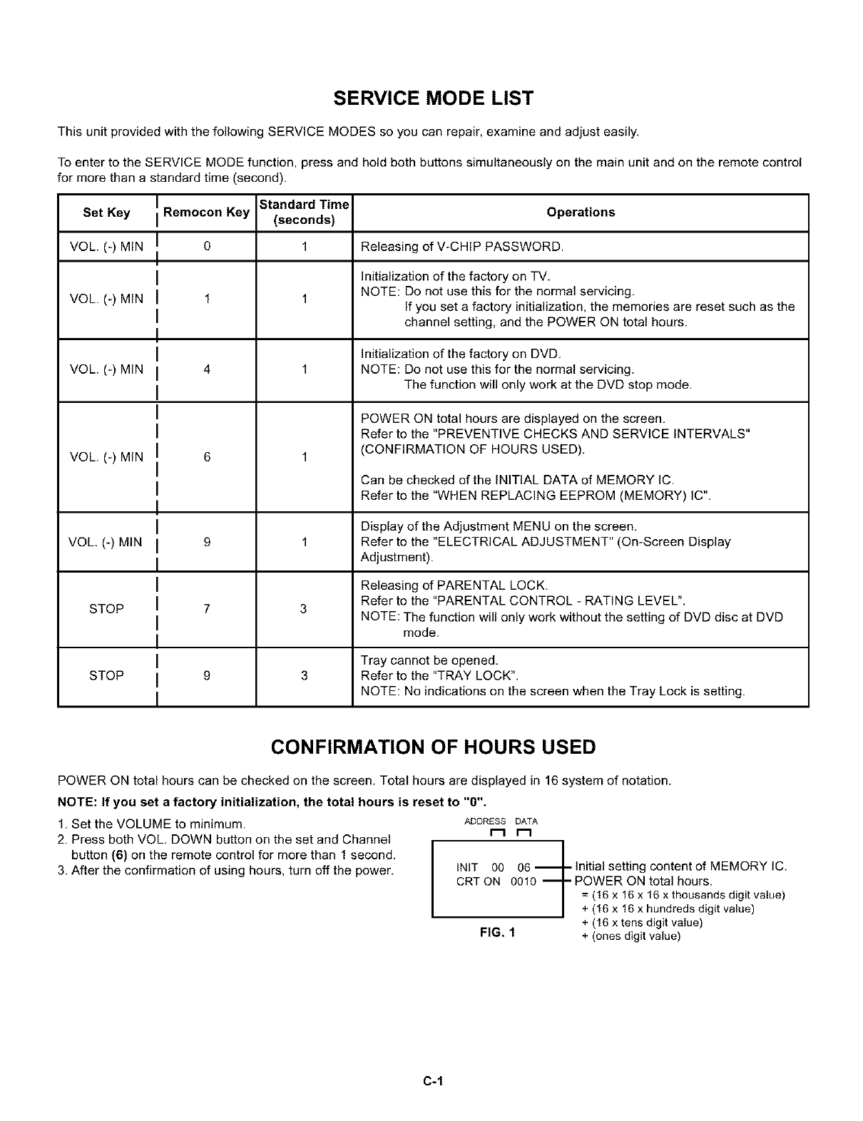
SERVICE MODE LIST
This unit provided with the following SERVICE MODES so you can repair, examine and adjust easily.
To enter to the SERVICE MODE function, press and hold both buttons simultaneously on the main unit and on the remote control
for more than a standard time (second).
Standard Tim_
Set Key Remocon Key (seconds) Operations
VOL. (_) MIN I0 1 Releasing of V-CHIP PASSWORD.
I
IInitialization of the factory on TV.
VOL. (_) MIN I 1 1 NOTE: Do not use this for the normal servicing.
If you set a factory initialization, the memories are reset such as the
Ichannel setting, and the POWER ON total hours.
I
I Initialization of the factory on DVD.
VOL. (_) MIN I 4 1 NOTE: Do not use this for the normal servicing.
IThe function will only work at the DVD stop mode.
I POWER ON total hours are displayed on the screen.
I Refer to the "PREVENTIVE CHECKS AND SERVICE INTERVALS"
VOL. (*) MINI 6 1 (CONFIRMATION OF HOURS USED).
ICan be checked of the INITIAL DATA of MEMORY IC.
I Refer to the "WHEN REPLACING EEPROM (MEMORY) IC".
I
I Display of the Adjustment MENU on the screen,
VOL. (_) MIN I 9 1 Refer to the "ELECTRICAL ADJUSTMENT" (On-Screen Display
I Adjustment).
I Releasing of PARENTAL LOCK.
STOP I 7 3 Refer to the "PARENTAL CONTROL _ RATING LEVEL".
I NOTE: The function will only work without the setting of DVD disc at DVD
I mode.
I Tray cannot be opened.
STOP I 9 3 Refer to the "TRAY LOCK".
I NOTE: No indications on the screen when the Tray Lock is setting.
CONFIRMATION OF HOURS USED
POWER ON total hours can be checked on the screen. Total hours are displayed in 16 system of notation.
NOTE: If you set a factory initialization, the total hours is reset to "0".
1. Set the VOLUME to minimum.
2. Press both VOL. DOWN button on the set and Channel
button (6} on the remote control for more than 1 second.
3. After the confirmation of using hours, turn off the power.
ADDRESS DATA
I INIT 00 06 _L Initial setting content of MEMORY IC.
CRT ON 0010 _ POWER ON total hours.
| = (16 x 16 x 16 x thousands digit value)
| + (16 x 16 x hundreds digit value)
+ (16 x tens digit value)
FIG. 1 + (ones digit value)
C-1
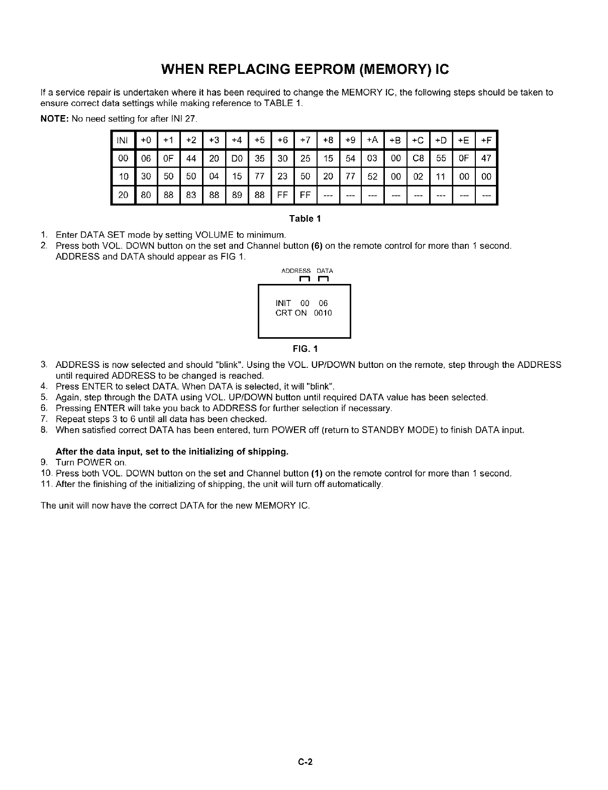
WHEN REPLACING EEPROM (MEMORY) IC
If a service repair is undertaken where it has been required to change the MEMORY IC, the following steps should be taken to
ensure correct data settings while making reference to TABLE 1.
NOTE: No need setting for after INI 27.
INI +O +1 +2 +3 +4 +5 +6 +7 +8 +9 +A +B +C +D +E +F
00 06 OF 44 20 DO 35 30 25 15 54 03 OO C8 55 OF 47
10 30 50 50 04 15 77 23 50 20 77 52 OO 02 11 OO OO
20 80 88 83 88 89 88 FF FF
Table 1
1. Enter DATA SET mode by setting VOLUME to minimum.
2. Press both VOL. DOWN button on the set and Channel button (6} on the remote control for more than 1 second.
ADDRESS and DATA should appear as FIG 1.
ADDRESS DATA
i
INIT 00 06 I
I
CRT ON 0010
FIG, 1
3. ADDRESS is now selected and should "blink". Using the VOL. UP/DOWN button on the remote, step through the ADDRESS
until required ADDRESS to be changed is reached.
4. Press ENTER to select DATA. When DATA is selected, it will "blink".
5. Again, step through the DATA using VOL UP/DOWN button until required DATA value has been selected.
6. Pressing ENTER will take you back to ADDRESS for further selection if necessary.
7. Repeat steps 3 to 6 until all data has been checked.
8. When satisfied correct DATA has been entered, turn POWER off (return to STANDBY MODE) to finish DATA input.
After the data input, set to the initializing of shipping.
9. Turn POWER on.
10. Press both VOL. DOWN button on the set and Channel button (1) on the remote control for more than 1 second.
11. After the finishing of the initializing of shipping, the unit will turn off automatically.
The unit will now have the correct DATA for the new MEMORY IC.
C-2
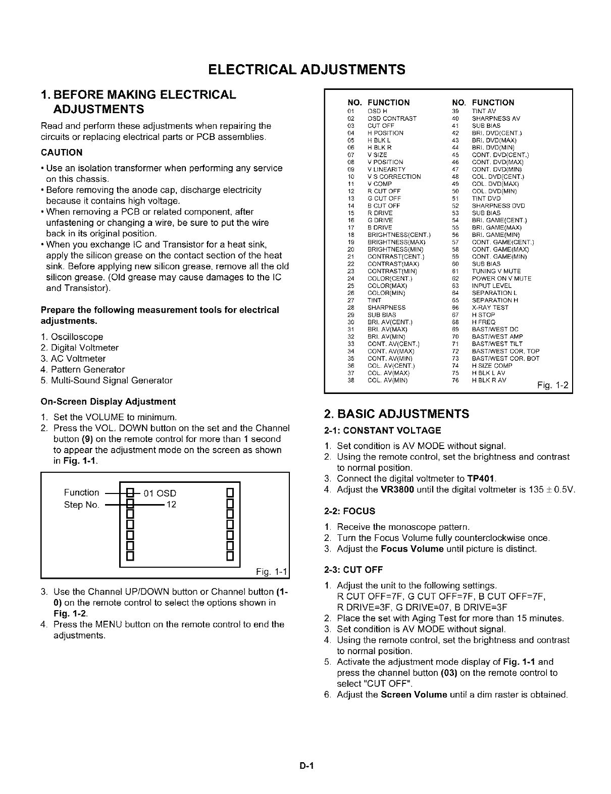
ELECTRICAL ADJUSTMENTS
1. BEFORE MAKING ELECTRICAL
ADJUSTMENTS
Read and perform these adjustments when repairing the
circuits or replacing electrical parts or PCB assemblies.
CAUTION
• Use an isolation transformer when performing any service
on this chassis.
• Before removing the anode cap, discharge electricity
because it contains high voltage.
• When removing a PCB or related component, after
unfastening or changing a wire, be sure to put the wire
back in its original position.
• When you exchange IC and Transistor for a heat sink,
apply the silicon grease on the contact section of the heat
sink. Before applying new silicon grease, remove all the old
silicon grease. (Old grease may cause damages to the IC
and Transistor).
Prepare the following measurement tools for electrical
adjustments,
1. Oscilloscope
2. Digital Voltmeter
3. AC Voltmeter
4. Pattern Generator
5. Multi-Sound Signal Generator
On-Screen Display Adjustment
1, Set the VOLUME to minimum,
2. Press the VOL. DOWN button on the set and the Channel
button (9} on the remote control for more than 1 second
to appear the adjustment mode on the screen as shown
in Fig. 1-1.
Function --
Step No.
-B-oiOSD O
[] 12 O
[] []
[] []
[] []
[] []
[] O
Fig. 1-1
3. Use the Channel UP/DOWN button or Channel button (%
0) on the remote control to select the options shown in
Fig, 1-2,
4. Press the MENU button on the remote control to end the
adjustments.
NO. FUNCTION NO. FUNCTION
01 OSD H 39 TINT AV
02 OSD CONTRAST 40 SHARPNESS AV
03 CUT OFF 41 SUB BIAS
04 H POSITION 42 BRI DVD(CENT)
05 H BLK L43 BRI DVD(MAX)
06 H BLK R 44 BRI DVD(MIN)
07 V SIZE 45 CONT DVD(CENT)
08 V POSITION 46 CONT DVD(MAX)
09 V LINEARITY 47 CONT DVD(MIN)
10 V S CORRECTION 48 COL DVD(CENT )
11 V COMP 49 COL DVD(MAX)
12 R CUT OFF 50 COL DVD(MIN)
13 G CUT OFF 51 TINT DVD
14 B CUT OFF 52 SHARPNESS DVD
15 R DRIVE 53 SUB BIAS
16 G DRIVE 54 BRI GAME{CENT )
17 B DRIVE 55 BRI GAME{MAX)
18 BRIGHTNESS{CENT ) 56 BRI GAME(MIN)
19 BRIGHTNESS{MAX) 57 CQNT GAME(CENT)
20 BRIGHTNESS{MIN) 58 CQNT GAME(MAX)
21 CONTRAST{CENT ) 59 CQNT GAME(MIN)
22 CONTRAST{MAX) 60 SUB BIAS
23 CQNTRAST{MIN) 61 TUNING V MUTE
24 COLOR(CENT ) 62 POWER QN V MUTE
25 COLOR(MAX) 63 iNPUT LEVEL
26 COLOR(MIN) 64 SEPARATION L
27 TINT 65 SEPARATION H
28 SHARPNESS 66 X-RAY TEST
29 SUB BiAS 67 H STOP
30 BRI AV(CENT ) 68 H FREQ
31 BRI AV(MAX) 69 BAST/WEST DC
32 BRI AV(MIN) 70 BAST/WEST AMP
33 CONT AV{CENT ) 71 BAST/WEST TiLT
34 CONT AV{MAX) 72 BAST/WEST COR, TOP
35 CONT AV{MIN) 73 BAST/WEST COR, BOT
36 COL AV(CENT) 74 H SIZE COMP
37 COL AV(MAX) 75 H BLK L AV
38 COL AV(MIN) 76 H BLK R AV Fig. 1-2
2. BASIC ADJUSTMENTS
2-1: CONSTANT VOLTAGE
1. Set condition is AV MODE without signal.
2. Using the remote control, set the brightness and contrast
to normal position.
3. Connect the digital voltmeter to TP401.
4. Adjust the VR3800 until the digital voltmeter is 135 _+0.5V.
2-2:FOCUS
1. Receive the monoscope pattern.
2. Turn the Focus Volume fully counterclockwise once.
3. Adjust the Focus Volume until picture is distinct.
2-3: CUT OFF
1. Adjust the unit to the following settings.
R CUT OFF=7F, G CUT OFF=7F, B CUT OFF=7F,
R DRIVE=3F, G DRIVE=07, B DRIVE=3F
2. Placethe set with Aging Test for morethan 15 minutes.
3. Set condition is AV MODE without signal.
4. Using the remote control, set the brightness and contrast
to normal position.
5. Activate the adjustment mode display of Fig. 1-1 and
press the channel button (03} on the remote control to
select "CUT OFF".
6. Adjust the Screen Volume until a dim raster is obtained.
D-1
ELECTRICAL ADJUSTMENTS
2-4: WHITE BALANCE
NOTE: Adjust after performing CUT OFF adjustment.
1. Place the set with Aging Test for more than 15 minutes.
2. Receive the gray scale pattern from the Pattern
Generator.
3. Using the remote control, set the brightness and contrast
to normal position.
4. Activate the adjustment mode display of Fig. 1-1 and
press the channel button (16) on the remote control to
select "G DRIVE".
5. Press the CH. UP/DOWN button on the remote control to
select the "R CUT OFF", "G CUT OFF", "B CUT OFF", "R
DRIVE" or "B DRIVE".
6. Adjust the VOL. UP/DOWN button on the remote control
to whiten the R CUT OFF, G CUT OFF, B CUT OFF, R
DRIVE, and B DRIVE at each step tone sections equally.
7. Perform the above adjustments 5 and 6 until the white
color is looked like a white.
2-5: HORIZONTAL POSITION
1. Receive the monoscope pattern.
2. Using the remote control, set the brightness and contrast
to normal position.
3. Activate the adjustment mode display of Fig. 1-1 and
press the channel button (04) on the remote control to
select "HPOSF.
4. Press the VOL. UP/DOWN button on the remote control
until the SHIFT quantity of the OVER SCAN on right and
left becomes minimum.
2-6: VERTICAL POSITION
1. Receive the monoscope pattern.
2. Using the remote control, set the brightness and contrast
to normal position.
3. Activate the adjustment mode display of Fig. 1-1 and
press the channel button (08) on the remote control to
select "VPOSF.
4. Check if the step No. V POSI is "02".
5. Adjust the VR401 until the horizontal line becomes fit
to notch of the shadow mask.
2-7: VERTICAL SIZE
1. Receive the monoscope pattern.
2. Using the remote control, set the brightness and contrast
to normal position.
3. Activate the adjustment mode display of Fig. 1-1 and
press the channel button (07) on the remote control to
select "VSIZE".
4. Press the VOL. UP/DOWN button on the remote control
until the Up/Down OVER SCAN Quantity becomes equal
to the Right/Left OVER SCAN Quantity.
5. Receive a broadcast and check if the picture is normal.
2-8: VERTICAL LINEARITY
NOTE: Adjust after performing adjustments in section 2-7.
After the adjustment of Vertical Linearity, reconfirm
the Vertical Position and Vertical Size adjustments.
1. Receive the monoscope pattern.
2. Using the remote control, set the brightness and contrast
to normal position.
3. Activate the adjustment mode display of Fig. 1-1 and
press the channel button (09) on the remote control to
select "VLIN".
4. Press the VOL. UP/DOWN button on the remote control
until the SHIFT quantity of the OVER SCAN on upside
and downside becomes minimum,
2-9: SEPARATION
Please do the method (1) or method (2) adjustment,
Method (1)
1. Set the multi_sound signal generator for each different L-
ch and R*ch frequency (Ex. L-ch=2KHz, R-ch=400Hz)
and receive the RF signal.
2. Connect the oscilloscope to the Audio Out Jack.
3. Press the AUDIO button on the remote control to set to
the stereo mode.
4. Activate the adjustment mode display of Fig. 1-1 and
press the channel button (64) on the remote control to
select "SEPAL".
5. Press the VOL. UP/DOWN button on the remote control
to adjust it until the audio output wave becomes a fine
sine wave.
6. Press the CH UP button 1 time to set to "SEPAH" mode.
7. Press the VOL. UP/DOWN button on the remote control
to adjust it until the audio output wave becomes a fine
sine wave.
Method (2)
1. Set the multi_sound signal generator L-ch=lKHz, R_ch
=Non input and receive the RF signal.
2. Connect the oscilloscope to the Audio Out Jack (R-eh).
3. Press the AUDIO button on the remote control to set to
the stereo mode.
4. Activate the adjustment mode display of Fig. 1-1 and
press the channel button (64) on the remote control to
select "SEPAL".
5. Press the VOL. UP/DOWN button on the remote control
to adjust it until the R-ch output becomes minimum.
6. Press the CH UP button 1 time to set to "SEPAH" mode.
7. Press the VOL. UP/DOWN button on the remote control
to adjust it until the R-ch output becomes minimum.
8. Set the multi*sound signal generator L-ch=Non input,
R-ch=l KHz and receive the RF signal.
9. Connect the oscilloscope to the Audio Out Jack (L-oh).
Then perform the above adjustments 3-7.
D-2
ELECTRICAL ADJUSTMENTS
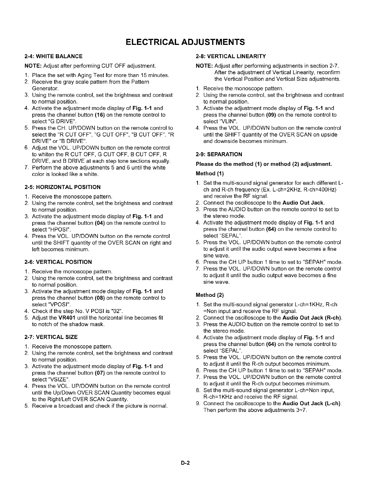
2-10: OSD HORIZONTAL
1, Activate the adjustment mode display of Fig, %1.
2. Press the VOL, UP/DOWN button on the remote control
until the difference of A and B becomes minimum.
(Refer to Fig, 2-1)
[] 01OSD 13
r_ 12 13
[] [3
[] 13
[] 13
[] 13
[] 13
[] [3
B
2-11: LEVEL
1. Receive the VHF HIGH (70dB).
2. Connect the AC voltmeter to pin 6 of CP101.
3. Activate the adjustment mode display of Fig. %1 and
press the channel button (63) on the remote control to
select "LVL".
4. Press the VOU UP/DOWN button on the remote control
until the AC voltmeter is 75 _+2inV.
2-12: BRIGHT CENTER
1. Receive the monoscope pattern. (RF Input)
2. Using the remote control, set the brightness and contrast
to normal position.
3. Activate the adjustment mode display of Fig. 1-1 and
press the channel button (18) on the remote control to
select "BRTC".
4. Press the VOL. UP/DOWN button on the remote control
until the white 15% is starting to be visible
5. Receive the monoscope pattern. (Audio Video Input)
6. Press the INPUT SELECT button on the remote control
to set to the AV mode.
7. Using the remote control, set the brightness and contrast
to normal position.
8. Activate the adjustment mode display of Fig. 1-1 and
press the channel button (30) on the remote control to
select "BRTCA".
9. Press the VOL. UP/DOWN button on the remote control
until the white 15% is starting to be visible
10. Press the TV/DVD button on the remote control to set to
the DVD mode.
11. Activate the adjustment mode display of Fig. 1-1 and
press the channel button (42) on the remote control to
select "BRTCD".
12. Press the VOL. UP/DOWN button on the remote control
to set the same step numbers as the AV.
13. Press the GAME button on the remote control to set to
the GAME mode.
14. Activate the adjustment mode display of Fig. 1-1 and
press the channel button (54) on the remote control to
select "BRTCG".
15. Press the VOL. UP/DOWN button on the remote control
to set the same step numbers as the AV. D-3
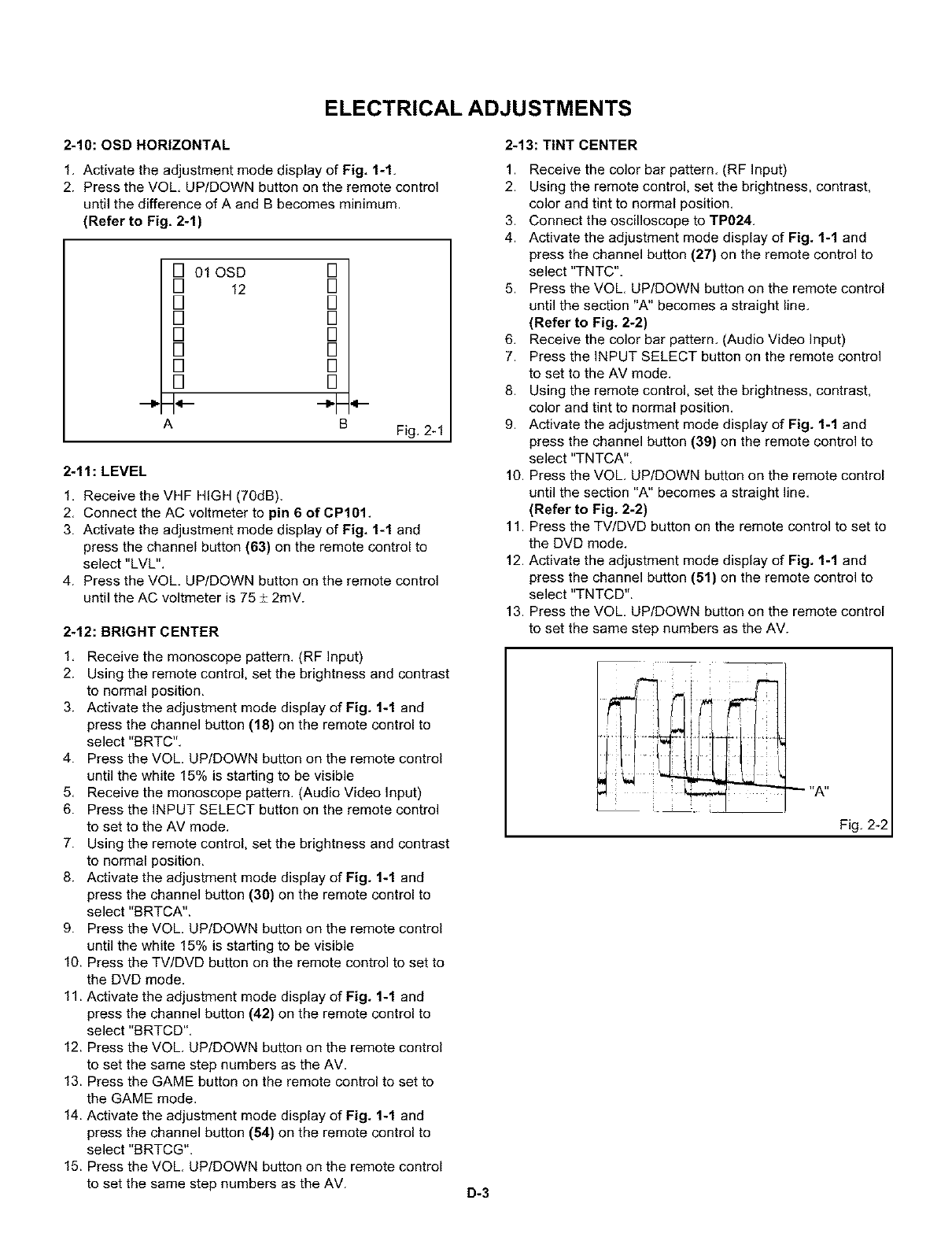
2-13: TINT CENTER
1. Receive the color bar pattern. (RF Input)
2. Using the remote control, set the brightness, contrast,
color and tint to normal position.
3. Connect the oscilloscope to TP024.
4. Activate the adjustment mode display of Fig. 1-1 and
press the channel button (27) on the remote control to
select "TNTC".
5. Press the VOL. UP/DOWN button on the remote control
until the section "A" becomes a straight line.
(Refer to Fig. 2-2)
6. Receive the color bar pattern. (Audio Video Input)
7. Press the INPUT SELECT button on the remote control
to set to the AV mode.
8. Using the remote control, set the brightness, contrast,
color and tint to normal position.
9. Activate the adjustment mode display of Fig. 1-1 and
press the channel button (39) on the remote control to
select "TNTCA".
10. Press the VOL. UP/DOWN button on the remote control
until the section "A" becomes a straight line.
(Refer to Fig. 2-2)
11. Press the TV/DVD button on the remote control to set to
the DVD mode.
12. Activate the adjustment mode display of Fig. 1-1 and
press the channel button (51) on the remote control to
select "TNTCD".
13. Press the VOL. UP/DOWN button on the remote control
to set the same step numbers as the AV.
ELECTRICAL ADJUSTMENTS
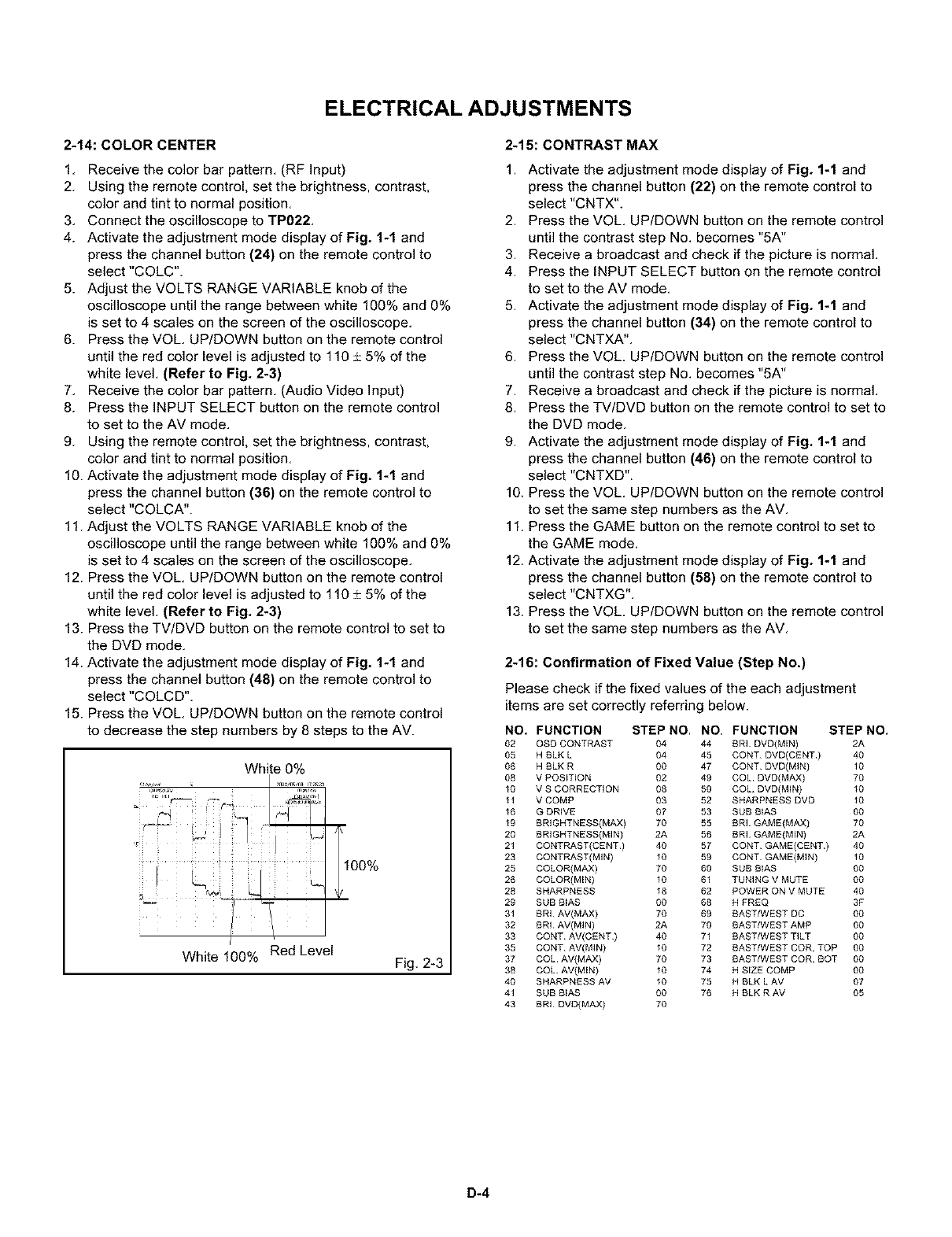
2-14: COLOR CENTER
1, Receive the color bar pattern, (RF Input)
2. Using the remote control, set the brightness, contrast,
color and tint to normal position,
3, Connect the oscilloscope to TP022,
4. Activate the adjustment mode display of Fig. %1 and
press the channel button (24) on the remote control to
select "COLC",
5. Adjust the VOLTS RANGE VARIABLE knob of the
oscilloscope until the range between white 100% and 0%
is set to 4 scales on the screen of the oscilloscope,
6. Press the VOL, UP/DOWN button on the remote control
until the red color level is adjusted to 110 _+5% of the
white level, (Refer to Fig. 2-3)
7, Receive the color bar pattern, (Audio Video Input)
8. Press the INPUT SELECT button on the remote control
to set to the AV mode.
9. Using the remote control, set the brightness, contrast,
color and tint to normal position,
10. Activate the adjustment mode display of Fig. %1 and
press the channel button (36) on the remote control to
select "COLCA".
11. Adjust the VOLTS RANGE VARIABLE knob of the
oscilloscope until the range between white 100% and 0%
is set to 4 scales on the screen of the oscilloscope,
12. Press the VOL, UP/DOWN button on the remote control
until the red color level is adjusted to 110 _+5% of the
white level. (Refer to Fig. 2-3)
13. Press the TV/DVD button on the remote control to set to
the DVD mode.
14. Activate the adjustment mode display of Fig. %1 and
press the channel button (48) on the remote control to
select "COLCD",
15. Press the VOL, UP/DOWN button on the remote control
to decrease the step numbers by 8 steps to the AV.
White 0%
-Jqi L
White 100% Red Level Fig, 2-3
2-15: CONTRAST MAX
1. Activate the adjustment mode display of Fig. %1 and
press the channel button (22) on the remote control to
select "CNTX".
2. Press the VOL, UP/DOWN button on the remote control
until the contrast step No. becomes "5A"
3. Receive a broadcast and check if the picture is normal.
4. Press the INPUT SELECT button on the remote control
to set to the AV mode,
5. Activate the adjustment mode display of Fig. 1-1 and
press the channel button (34) on the remote control to
select "CNTXA",
6. Press the VOL, UP/DOWN button on the remote control
until the contrast step No. becomes "5A"
7. Receive a broadcast and check if the picture is normal.
8. Press the TV/DVD button on the remote control to set to
the DVD mode,
9. Activate the adjustment mode display of Fig. 1-1 and
press the channel button (46) on the remote control to
select "CNTXD".
10. Press the VOL, UP/DOWN button on the remote control
to set the same step numbers as the AV,
11. Press the GAME button on the remote control to set to
the GAME mode,
12. Activate the adjustment mode display of Fig. 1-1 and
press the channel button (58) on the remote control to
select "CNTXG",
13. Press the VOL, UP/DOWN button on the remote control
to set the same step numbers as the AV,
2-16: Confirmation of Fixed Value (Step No,)
Please check if the fixed values of the each adjustment
items are set correctly referring below.
NO. FUNCTION STEP NO.
02 OSD CONTRAST 04
05 H BLK L 04
06 H BLK R O0
08 V POSiTiON 02
10 V S CORRECTION 08
11 V COMP 03
16 G DRIVE 07
19 BRIGHTNESS(MAX) 70
20 BRIGHTNESS(MIN) 2A
21 CONTRAST(CENT) 40
23 CONTRAST(MIN) 10
25 COLOR(MAX) 70
26 COLOR(MIN) 10
28 SHARPNESS 18
29 SUB BIAS O0
31 BRI AV(MAX) 70
32 BRI AV(MIN) 2A
33 CONT AV(CENT ) 40
35 CONT AV(MIN) 10
37 COL AV(MAX) 70
38 COL. AV(MIN) 10
40 SHARPNESS AM 10
41 SUB BiAS O0
NO. FUNCTION STEP NO.
44 BRI DVD(MIN) 2A
45 CONT DVDICENT )40
47 CONT DVDIMIN )10
49 COL DVD(MAX) 70
50 COL. DVD(MIN) 10
52 SHARPNESS DVD 10
53 SUB BIAS O0
55 BRI GAME(MAX) 70
56 BRI GAME(MIN) 2A
57 CQNT GAME(CENT) 40
59 CONT GAME(MIN) 10
60 SUB BiAS O0
61 TUNING V MUTE O0
62 POWER QN V MUTE 40
68 H FREQ 3F
69 BAST/WEST DO O0
70 BAST/WEST AMP O0
71 BAST/WEST TILT O0
72 BAST/WEST COR, TOP O0
73 BAST/WEST COR, BOT O0
74 H SiZE COMP O0
75 H BLK L AM 07
76 H BLK R AV 05
43 BRI DVD(MAX) 70
D-4
ELECTRICAL ADJUSTMENTS
3. PURITY AND CONVERGENCE
ADJUSTMENTS
NOTE
1. Turn the unit on and let it warm up for at least 30
minutes before performing the following adjustments.
2. Place the CRT surface facing east or west to reduce the
terrestrial magnetism.
3. Turn ON the unit and demagnetize with a Degauss Coil.
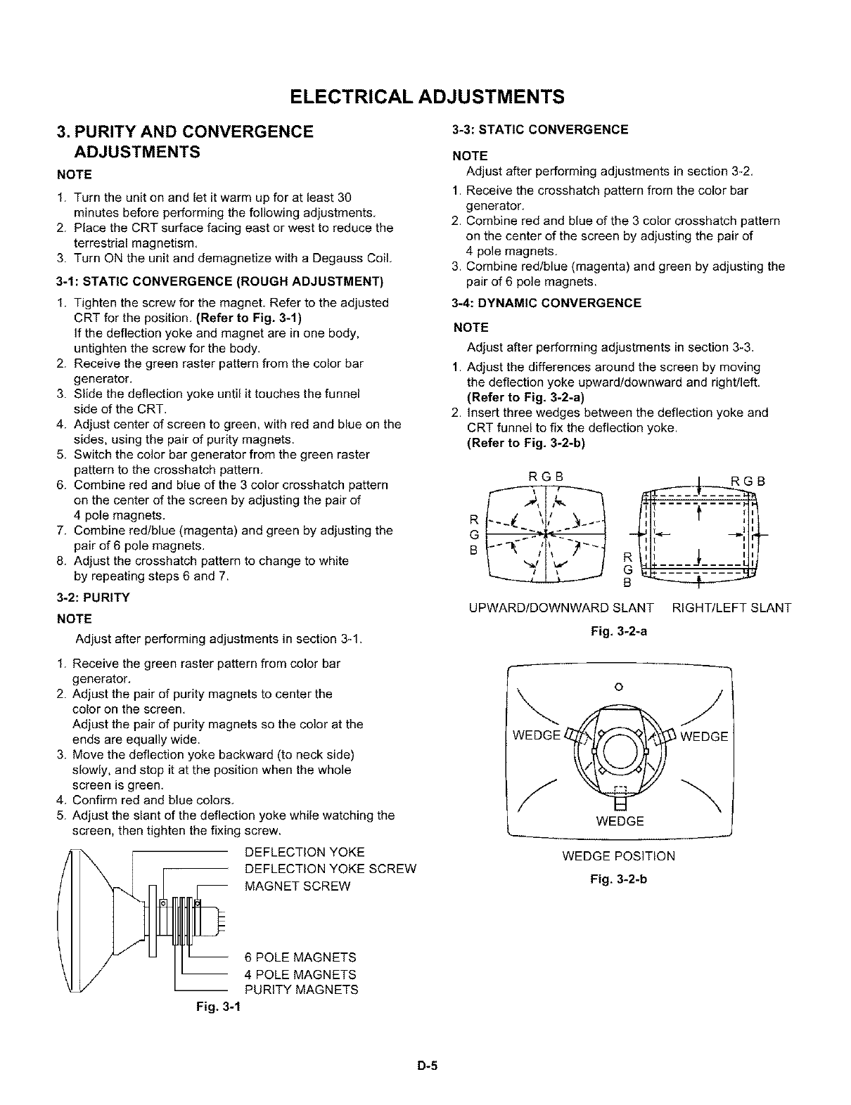
3-1: STATIC CONVERGENCE (ROUGH ADJUSTMENT)
1. Tighten the screw for the magnet. Refer to the adjusted
CRT for the position. (Refer to Fig. 3-1)
If the deflection yoke and magnet are in one body,
untighten the screw for the body.
2. Receive the green raster pattern from the color bar
generator.
3. Slide the deflection yoke until it touches the funnel
side of the CRT.
4. Adjust center of screen to green, with red and blue on the
sides, using the pair of purity magnets.
5. Switch the color bar generator from the green raster
pattern to the crosshatch pattern.
6. Combine red and blue of the 3 color crosshatch pattern
on the center of the screen by adjusting the pair of
4 pole magnets.
7. Combine red/blue (magenta) and green by adjusting the
pair of 6 pole magnets.
8. Adjust the crosshatch pattern to change to white
by repeating steps 6 and 7.
3-2: PURITY
NOTE
Adjust after performing adjustments in section 3-1.
1. Receive the green raster pattern from color bar
generator.
2. Adjust the pair of purity magnets to center the
color on the screen.
Adjust the pair of purity magnets so the color at the
ends are equally wide.
3. Move the deflection yoke backward (to neck side)
slowly, and stop it at the position when the whole
screen is green.
4. Confirm red and blue colors.
5. Adjust the slant of the deflection yoke while watching the
screen, then tighten the fixing screw.
DEFLECTION YOKE
DEFLECTION YOKE SCREW
MAGNET SCREW
Fig. 3-1
6 POLE MAGNETS
4 POLE MAGNETS
PURITY MAGNETS
3-3: STATIC CONVERGENCE
NOTE
Adjust after performing adjustments in section 3-2.
1. Receive the crosshatch pattern from the color bar
generator.
2. Combine red and blue of the 3 color crosshatch pattern
on the center of the screen by adjusting the pair of
4 pole magnets.
3. Combine red/blue (magenta) and green by adjusting the
pair of 6 pole magnets.
3-4: DYNAMIC CONVERGENCE
NOTE
Adjust after performing adjustments in section 3-3.
1. Adjust the differences around the screen by moving
the deflection yoke upward/downward and right/left.
(Refer to Fig, 3-2-a)
2. Insert three wedges between the deflection yoke and
CRT funnel to fix the deflection yoke.
(Refer to Fig, 3-2-b)
R
G
B
RGB
UPWARD/DOWNWARD SLANT RIGHT/LEFT SLANT
Fig, 3-2-a
O
WEDGE_WEDGE
WEDGE
WEDGE POSITION
Fig, 3-2-b
D-5
ELECTRICAL ADJUSTMENTS
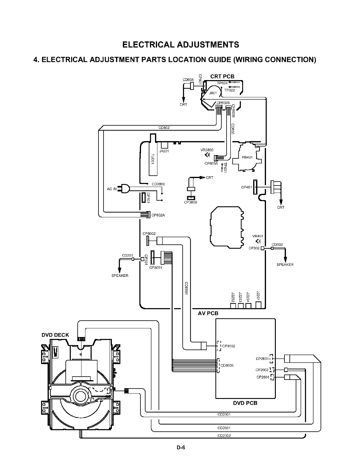
4. ELECTRICAL ADJUSTMENT PARTS LOCATION GUIDE (WIRING CONNECTION)
DVD DECK
/
AC IN _S"
CRT PCB
CD805 o_
o TP024
CP802B
CRT o
VR3800
1,1
CP803A
CD3800 S
ID° 1=1 CP401
_'_ CP802A
c_
CD301
CP8001
SPEAKER
CP3800
VR4C
CP302
AV PCB
ICP8502
iJ
r_
nnn F
i
I CD8505
CRT
CD302
SPEAKER
DVD PCB
CD2301
D-6
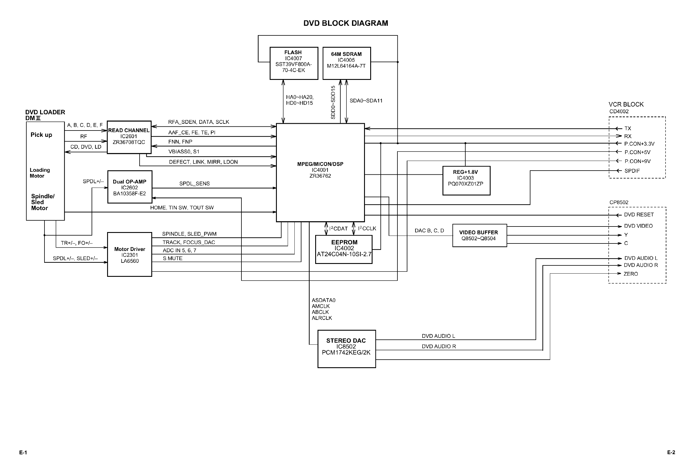
DVD BLOCK DIAGRAM
DVD LOADER
DM_
Pick up
Loading
Motor
Spindle/
Sled
Motor
A, B, C, D, E, F i "_
READ CHANNEL]
RF IC2601 I
ZR36708TQC i
CD, DVD, LD '_
I'
RFA SDEN, DATA, SCLK
AAF CE, FE, TE, PI
FLASH
IC4007
SST39VF800A-
70-4C-EK
HA0~HA20,
HD0-HD15
64M SDRAM
IC4005
M12L64164AWT
£3
co SDA0~SDA11
t
O
£3
£3
CO tr
SPDL+/- I Dual OP-AMP
IC2602
BA10358F-E2
FNN, FNP
VBIASS0, $1
DEFECT, LINK, MIRR, LDON
SPDL SENS
MPEG/MICON/DSP
IC4001
ZR36762
TR+/-, FO+/-
SPDL+/-, SLED+/-
Motor Driver
IC2301
LA6560
HOME, TIN SW, TOUT SW
SPINDLE, SLED PWM
TRACK, FOCUS DAC
ADC IN 5, 6, 7
S MUTE
;12CDAT ; 12CCLK
EEPROM /
tC4002 I_
AT24C04N-10SI-2.7J
ASDATA0
AMCLK
ABCLK
ALRCLK
fSTEREO DAC
IC8502
PCM1742KEG/2K
T
REG+I.8V
IC4003
PQ070XZ01ZP
DAC B, C, D VIDEO BUFFER
Q8502~Q8504
DVD AUDIO L
DVD AUDIO R
VCR BLOCK
CD4002
I
I
' ( TX
I
I
i > RX
i
, ( P.CON+3.3V
i
I(P.CON+5V
I
I
,(P.CON+9V
I
t(SPDIF
I
I
CP8502
I
I(DVD RESET
I
I
I 31 DVD VIDEO
I
I
i _ y
I
I :ii C
I
I
I
I3, DVD AUDIO L
i
I
,>DVDAUDIO R
I
I 31 ZERO
I
I
E-1 E-2
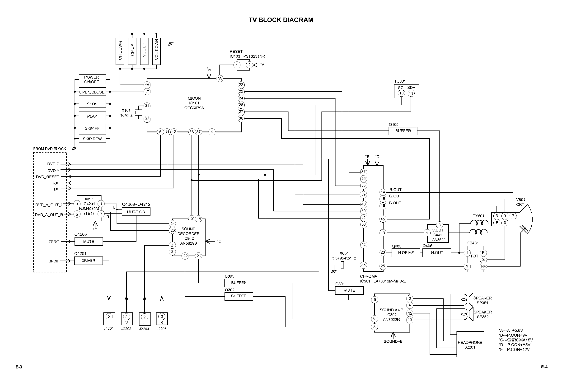
TV BLOCK DIAGRAM
FROM DVD BLOCK
I
I
I
DVD C I
i)
DVDY I)
I
DVDRESET i(
I
RX I<
TX I)
I
POWER
ON/OFF
OPEN/CLOSE
STOP
PLAY
SKiP FF
SKiP REW
I
Xl0116MHz
I
l [ AMP ]
DVD A OUT L _-'_'-_3_ IC4201 _1_ Q4209-Q4212
- - - _ 1 NJM4580M I L__ I
f--_ _TEI' _ MUTESW I
RESET
IC103 PST3231NR
MiCON
IC101
OEC6079A
*A
I/
*B *C
#
TU001
SCL SDA
Q105
[ BUFFER t
R.OUT
G,OUT
B.OUT V801
Q4203
ZERO :'_ MUTE I
I
I
IQ4201
I
sPo,F oR,VERF
I
I
J4201 J2202
'_ DECORDER
110902 _-_ *D
Jk t
J2204 J2203
Q3O5
[ BUFFER ]
Q302
I BUFFER t
X601
3.579545MHz
Q3Ol
_1 MUTE
L
Q4O5
H.DRIVE
CHROMA
IC601 LA76319M-MPB-E
I i •
? SOUND AMP
IC302
AN7522N I
4_
SOUND+B
: DY801 L_ I
Q406 - _ I rE2222--i
t__l
_ dSPEAKER
_J SP351
o)¢IsPEAKER
.)_J SP352
_ HEADPHONE
J2201
*A---AT+5.6V
*B---P.CON+9V
*C---CHROMA+5V
*D---P,CON+A5V
*E---P.CON+12V
E-3 E-4
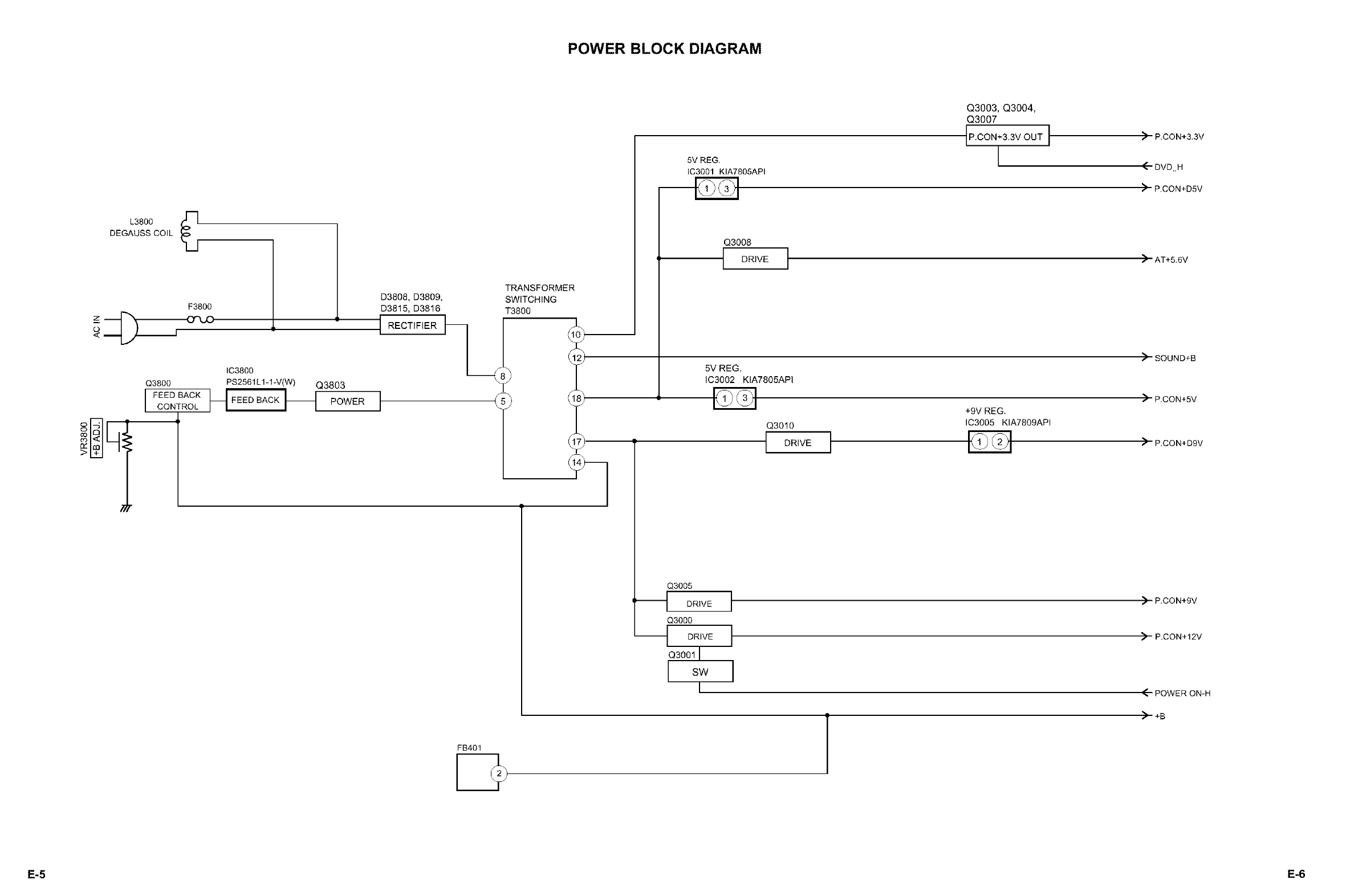
POWER BLOCK DIAGRAM
L3800
DEGAUSS COIL
F3800
__J
Q3800
FEED BACK
CONTROL
IC3800
PS2561Ll-l-V(W) Q3803
powER
TRANSFORMER
D3808, D3809, SWITCHING
D3815, D3816 T3800
I
FB40t
5V REG.
IC3001KIA7805API
Q3003, Q3004,
Q3007
IP.OON+3.3VOUT I
I
Q3005
OR,VEI
Q3000
--{ ORIVE1
Q30017
1
5V REG.
IC3002 KIA7805API
Q3010
I O_lWI
+9V REG.
IC3005 KIA7809API
1
P.CON+3.3V
< DVDH
) P.CON+D5V
AT+5.6V
SOUND+B
P.CON+5V
) P.CON+D9V
) P.CON+9V
) P.CON+t2V
POWER ON-H
) +S
E-5 E-6
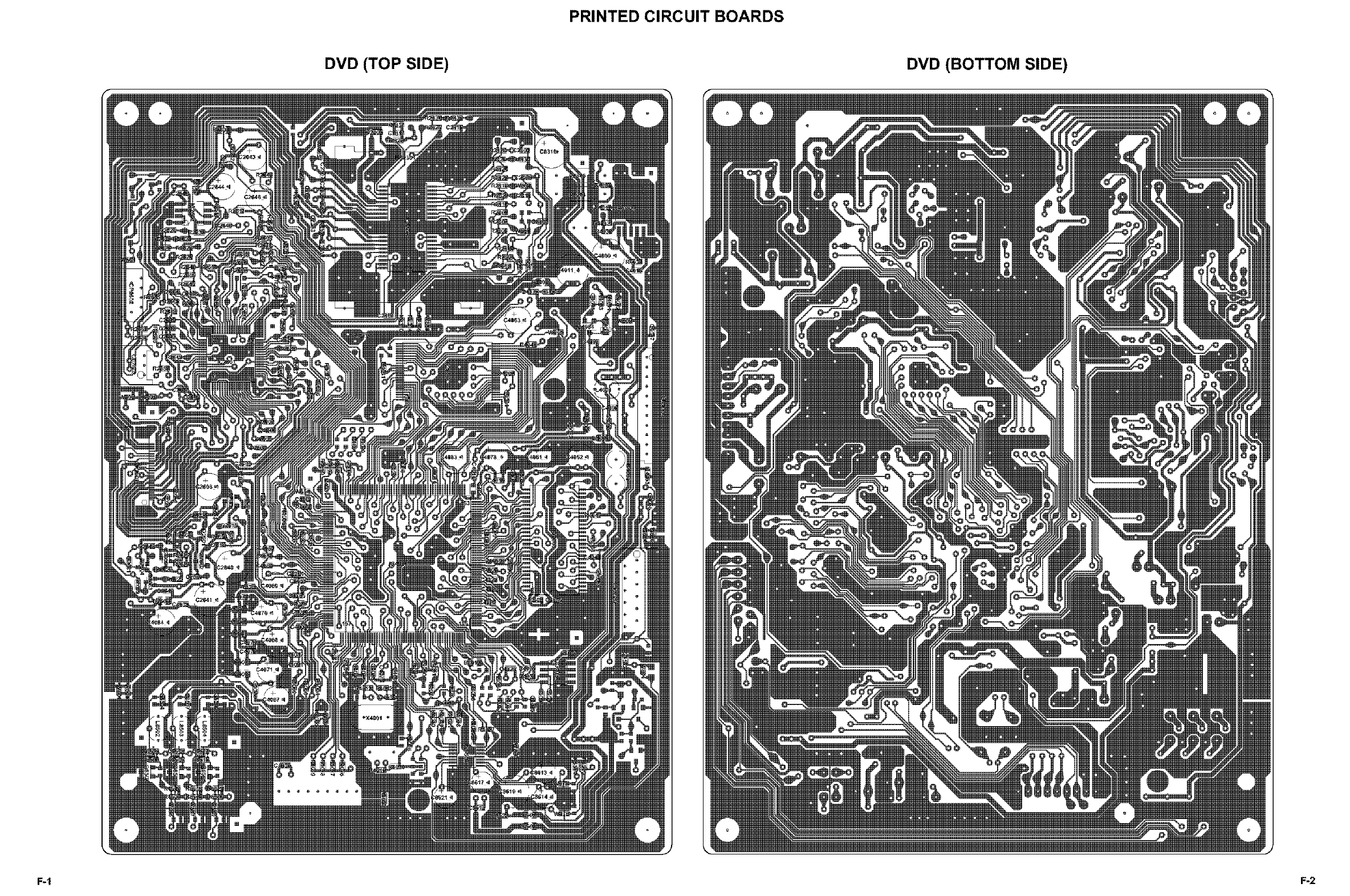
DVD (TOP SIDE)
PRINTED CIRCUIT BOARDS
DVD (BOTTOM SIDE)
F-I F-2
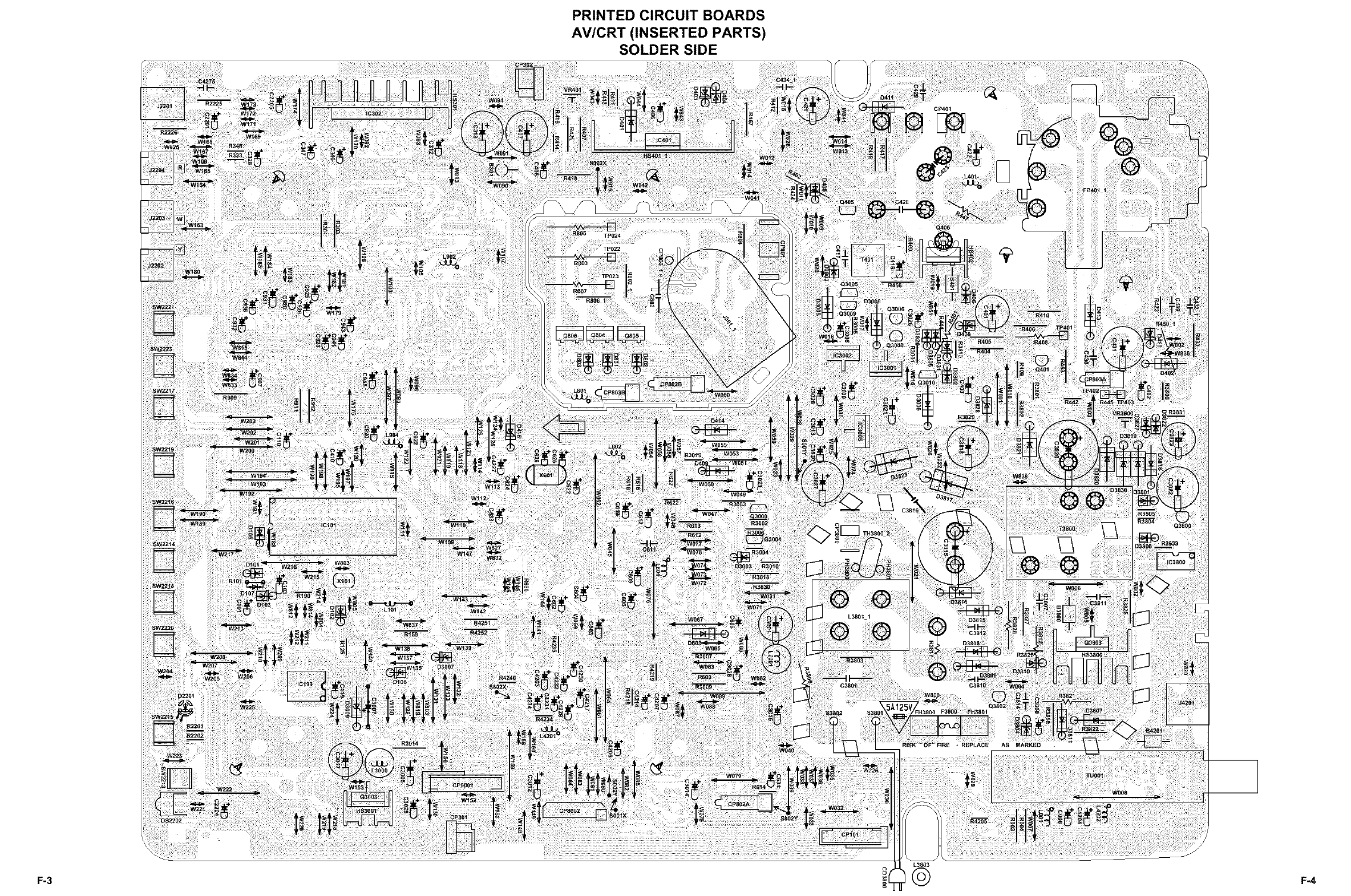
PRINTED CIRCUIT BOARDS
AV/CRT (INSERTED PARTS)
SOLDER SIDE
F-3 F-4
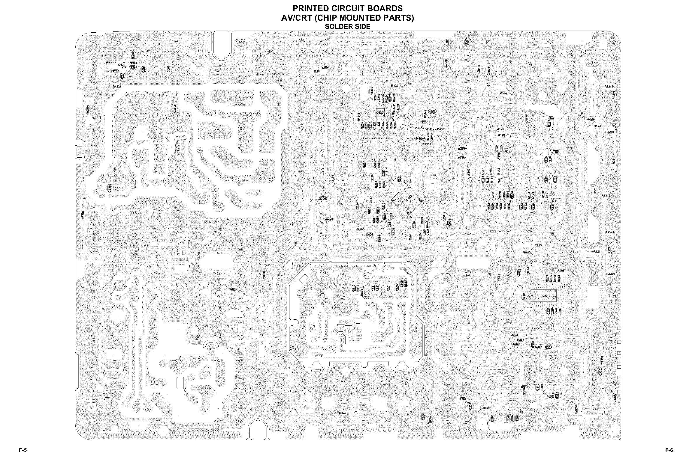
PRINTED CIRCUIT BOARDS
AV/CRT (CHIP MOUNTED PARTS)
SOLDER SIDE
F-5 F-6
PRINTED CIRCUIT BOARDS
RELAY (INSERTED PARS)
SOLDER SIDE
RELAY (CHIP MOUNTED PARS)
SOLDER SIDE
S_0_SX
S_O01X
S_O03X
SW
SOLDER SIDE
F-7 F-8
D GND
P CON+3 3V (
A I B I o I D I E I F I G I H
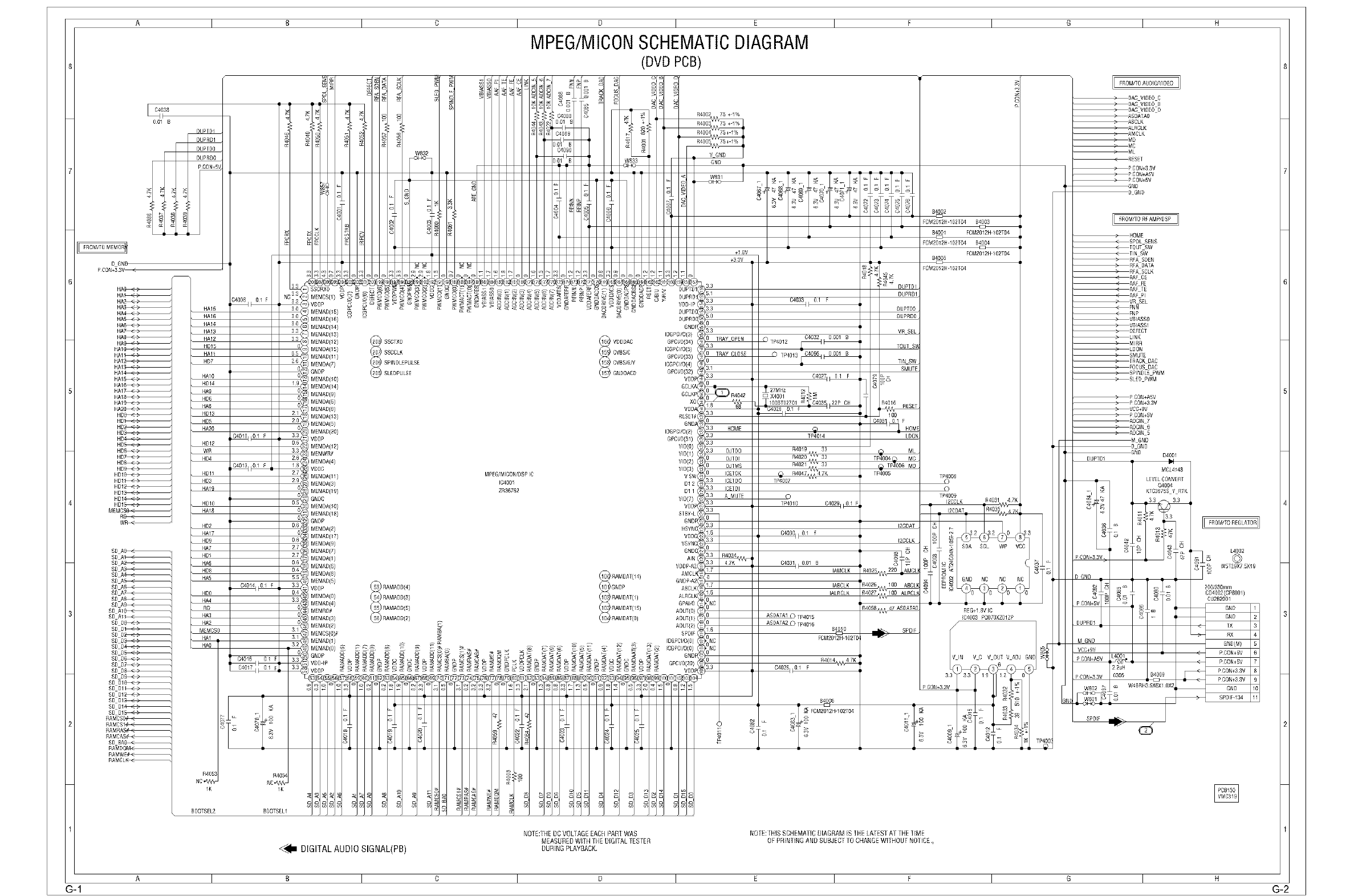
MPEG/MIOONSCHEMATICDIAGRAM
(DVD PCB)
0(}1 B
HA_
HA_
HA_
HA3_
HA,_
HA_.
HA_ _
HA,_
HAS_
HA_
HAI_
HAI_
HA1
HAI_
HAI_
HAI_
HAI_
HAI_
HAI_
HAI_
HA2_
HD_
HD_
HD_
HD_
HD_
HD_
HD6_
HD,_
HDS_
HD_
HDI_
HDI_
HDI_
HDI_
HDI_
HDI_
MEMC_
R[_
SD
SD I
D-J
SD I
SD-J
SD-J
SD I
SD
SD
SD
SD
SD
SD
DUPTDI
JPRDI
JPTDO
JPRDO
CON+5_
JU(_
JU_
Ja_
_aR_
z6_
_z
(c
D6_
27_
27_
D6_
D4_,
55_
33_
D4_
32_
SSORXD & --
MEMCSU) _
VgDP .....
MEMADDS) _
MEMADD6) .....
MEMADD4 )
MEMADD3 )
MEMADD2 )
MEMDAD5 )
MEMADDI )
MEMDA(7}
GNDP
MEMADDO )
MEMDAD4 )
MEM6D(9}
MEMDA(6}
MEMAD(8}
MEMDAD3 )
MEMDA(5}
MEMAD(20)
VgDP
MEMDAD2 )
MEMWR#
MEMDA(4}
VgDC
MEMDADI )
MEMDA(3}
MEMADD9 )
GNDC
MEMDADO )
MEMADD8 )
GNDP
MEMDA(2}
MEMADD7 )
MEMDA(9}
MEMAD(7}
MEMDAD}
MEMAD(6}
MEMDA(8}
MEMAD(5}
VgDP
MEMDA(O}
MEMAD(4}
MEMRD#
MEMAD(3}
MEMAD(2}
ooooooo
,- <<<<<<<<
IDGPCI/O(3}
SSCTXD G901/0{34)
SSCCLK IOGPCFO(5)
G_01/0{33)
SPINDLEP_LSE IOGPCFO(4)
SLEDPULSE G#CI/0{32)
MPEG/MICON/DSPIC
104001
ZR36762
IDGPCI/O(2}
GPCI/O{31)
WD((})
VID(I)
WD(2)
VID(3)
WD(7)
$TBY-L
GPAI/O
AOUT(0}
AOUTD}
_,OUT(2}
SPDIF
MEMCS((})#
MEMADD} __ _ =_ _ DGPCI/O(O)
v GND
W831
+_ 8V
+3 3V
04(}33 0 I F
4_
TP4014
R4019 33
TP4007
C)
TP4010
F
B
IAMCLK
IABCLK
IALROLK
B4010
R4014
F
B4006
FCM2012H 02704
TP4005
_i=i
B4002
FC_2012H-IO2T04 B4003
B4001 FCM2012H _02T(}4
FC_2012H-IO2T04 B4004
FCM2012H _02T(}4
B4005
FC_2012H-IO2T04
VR SEt
TOUT $I
TIN SW
RESE]
TP4008
©
©
TP40(}9
12CCLK
12CDA7
12CCLK
SDA SCL WP V_C
GND NC NC
REG+I 8V IC
104003 POOTOXZOIZP
V C V O_T V ADJ
%
_z
IK
BOOTSEL2 BOOTSELI
_1_ DIGITALAUDIOSIGNAL(PB)
NOIE:TRE DC VOL[AGE EACH PARr WAS
MEASURED WI[H IRE DIGIfAL IESfER
DURENGPLAYBACK
NO[E: fRIS SCH£MATIC DIAGRAM iS IRE LATESf A] [RE liME
OF PRENlING AND SU&fEC f TO CHANGEWI[HOU f NOTIC_ o
[[ FROM/TO AUD ONID£O ]]
_DAC VIDEO C
_DAC VIDEO 8
_DAC VIDEO D
_ASDATAO
_ABCLK
_ALRCLK
_AMCLK
_MD
_MC
_ML
_RESET
_N_
D GND
[[ FROM/TO RF AMP/DSP
SW
[E
F
7RSEL
_[DAC
I-
GNO
OGND
GND D001
D PTDI
MOL4148
LEVELCONVERT
04004
K703875S Y RTK
FROMF[O REGLA70 R]]
L4002
©
W5T29×7 5X19
20(}/330mm
CD4002(CPSO01)
CU2B2001
A I _ I o I D I E I F I G I H
G_I G-2
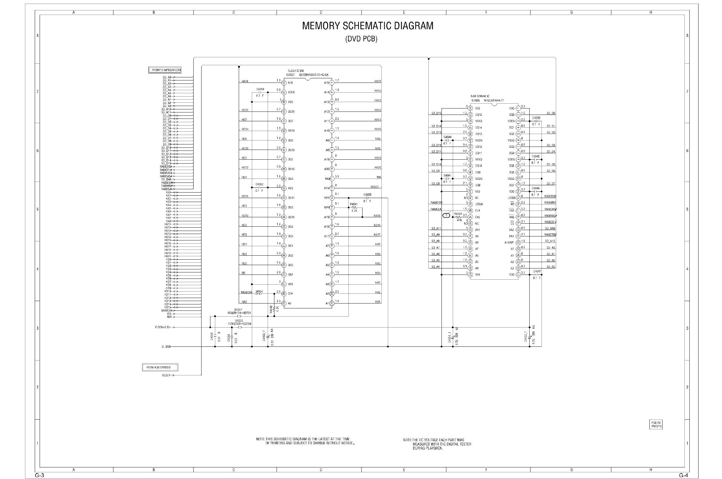
A I B I o I D I E I F I G I H
MEMORYSCHEMATICDIAGRAM
(DVD PCB)
SO A_
SO A_
SO A_
SO
SO
SO A_
SO A"
SO A_
SO A_
S{) A_
SD AI_
SD AI_
SO D_
SO DI_
SO D_
SO D_
SO D_
$9 D_ _
$9 D_ .
SO D7_
SO DS_
SD D_
SD DI_
SD DI_
SD DI _ -
SD DI_
SD DI_
SD DI_
RAMCS_
RAMCSI_
RAMRA"
RAMCA_
SD B_
RAMD_
RAMW_
RAMCL4_--
HA_
HA_
HA
HA_
HA_
HA= .
HA_ _
HA_
HA_
HA_
HAI_
HA1 : .
HAI_
HA1" _
HAI_ -
HAI_ _
HAI_
HAI_
HAI_
HA1r -
HA2_
HD_
HD_ _
HD_
HD" .
HD _
HD_ _
HD_ _
HD_
HD_
HD_
HDI_
HDI_
HDI_
HDI_
HDI_
HDlr _
M MCS4_;_
R_
W_
PCON+33V )
D GND
R£SE_
_D15
_D14
_D13
_D12
_D11
@3
HDIO
@2
HD£
@1
@8
HDO
RD
MEMCS(
HAO
B4007
FCM2012_402T04
04064
C40_2
FLAS C 8M
104007 SST39VFSOOA-70-4C-£K
A15(
VCCQ A14(
VSS A13(
A12(
A11(
AIO(
A_(
AS(
A19(
A20(
WE_
R_
VPP(
w_
A19(
A18(
A17(
AT(
A6(
AS(
A4(
VSS A3(
CE# A2(
AI(
_AI
_AI&
_A13
_AIZ
_A11
_AI_
HA9
HA8
_AI2
0_A2_
WE
RESET
C4039
01 F
01 R4041
HA18
HA17
HA7
HA6
HA5
HA4
HA3
HA2
HA1
SD D15 _2
q
SD D14 _5
SD D13 20
04040 33
Z
SD D12 01 F O4
SD Dll 0
q
SD DIO
SD D8 01 F 21
' i
RAMDQ_
RAMCL_
47K {
NC
SD A11 0
SD A9 02
SD A8 02
SD A7 _0
SD A6 _0
SD A5 _0
SD A4 09
64M SDRAM IC
104005 M12L64164A-7T
, VSS
, DO15
, VSSQ
, DO14
, DO13
, VDDQ
, DO12
, DO11
, VSSQ
, DQIO
DOg
, VDDQ
, DO8
, VSS
, NC
, UDOM
CLK
, CK£
, NC
, A11
, A9
, A8
, A7
, A6
, A5
, A4
, VSS
SD
C4050
NO[E: [HIS SCHEMA7 IC DIAGRAM IS filE LA]ES f Af THE HME
OF PRIN lING AND SUBJECT 10 CHANGEWITHOUT NOflCE. NO[E:fHE DC VOLTAGEEACH PAR[ WAS
MEASURED WIIH THE DIGllAL [ESlER
DURING PLAYBACK¸
A I B I o I D I E I _ I G I H
G-3 G-4
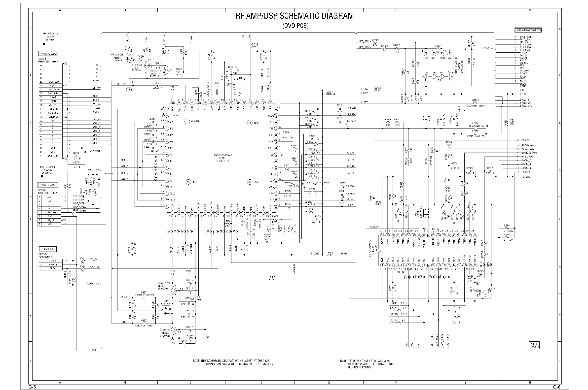
A I B I o I D I E I F I G I H
RFAMP/DSPSCHEMATICDIAGRAM
FFC(P_O5mm)
CD2601
2H001901
CP2601
IMSA.9631S.24Y901
[[C(P_I Omm)
CD2602
2H080701
CP2603
A2OOIWR2 3P
TR-
TR+
FO+
DWPD
.NC
VR DV/
DVDLD
CDLD
CDPD
OPU RF
OPU
OPU
OPU
OPU
OPU
OPU
OPU VRE_
C2648
01 F
PCON4G 3V
1(}0
1(}0
PCON+33V
D GNO
VR DVD CTL 0 R2620
02603 G
2SK3018 5
0 _n R2647G R2647
VR CD CT f_^^_
02604
2SK3018
TP8 °
OPU RF _/_3 C21613a
oool B
(DVD PCB)
==
RF GND
W8(}7 D GND
TP_5
OPU D I
OPU C I
OPU B I
OPU A !
NCO,
NCO,
C2603
II 25
(}0(}22 B
C2_(}4 II
(}0(}22 B
(}0(}22 B
(}0(}22 B
TP19
27
TP20
27
TP21
¢_ 27
TP22
27
27
27
2_
bVb LD CTL
02601
B2601
DVDLD
CDLD B2602
FCM2012H 102T04
02_(}2
2SA1036K
DVDRFN
A2
0 B2
C2
D2
C_
CN
)B
),_
_CD D
_CDC
_CD B
w d_
_1 o I
517 51 51
TP043 TP39
c_
R2_15
( ,
)
)40
(
45 2618 TP42
18
RfiAD CNANNELIC
_02601
ZR36708TQC
02 02 I (} 33 (}
260
47K
i
SDATA(
SCLK(
v33(
LCP(
LCN(
MNTR(
c_(
FE(
TE (
m(
V25(
V125(
TPH(
DFT(
I n _
IK
. 00056 B
1 2K
C2_18
C2615
IK
:_22 R2602
I zzt' C2655
(}01 B
R_ GNO
<+
_) R_A SDEr
TP_6
R_A DATI
TP_7
_ RFA SCL
TP18
AAF
AAF
AAF
AAF
+4% TP26
_) VBIASS0
TP38
VBIASS1
T_5 DEFECT
TP33
@ LINK
PCON+£V
W808 SGND
C2302 01 B
01 B
TOUTSW
0£
GND
NOTE:fills SCHEMATIC DIAGRAM IS IHE LAFESI AT IHE lIME
O_ PRINTING AND SUR_EC[ TO CHANGE WITHOUT NOTICEo NOIEHHE DC VOL[AGE EACH PAR[ WAS
MEASURED WI[H ]HE DIGITAL TES[ER
DURING PLAYRACK
A I B I o I D I E I _ I G I H
G-5 G-6
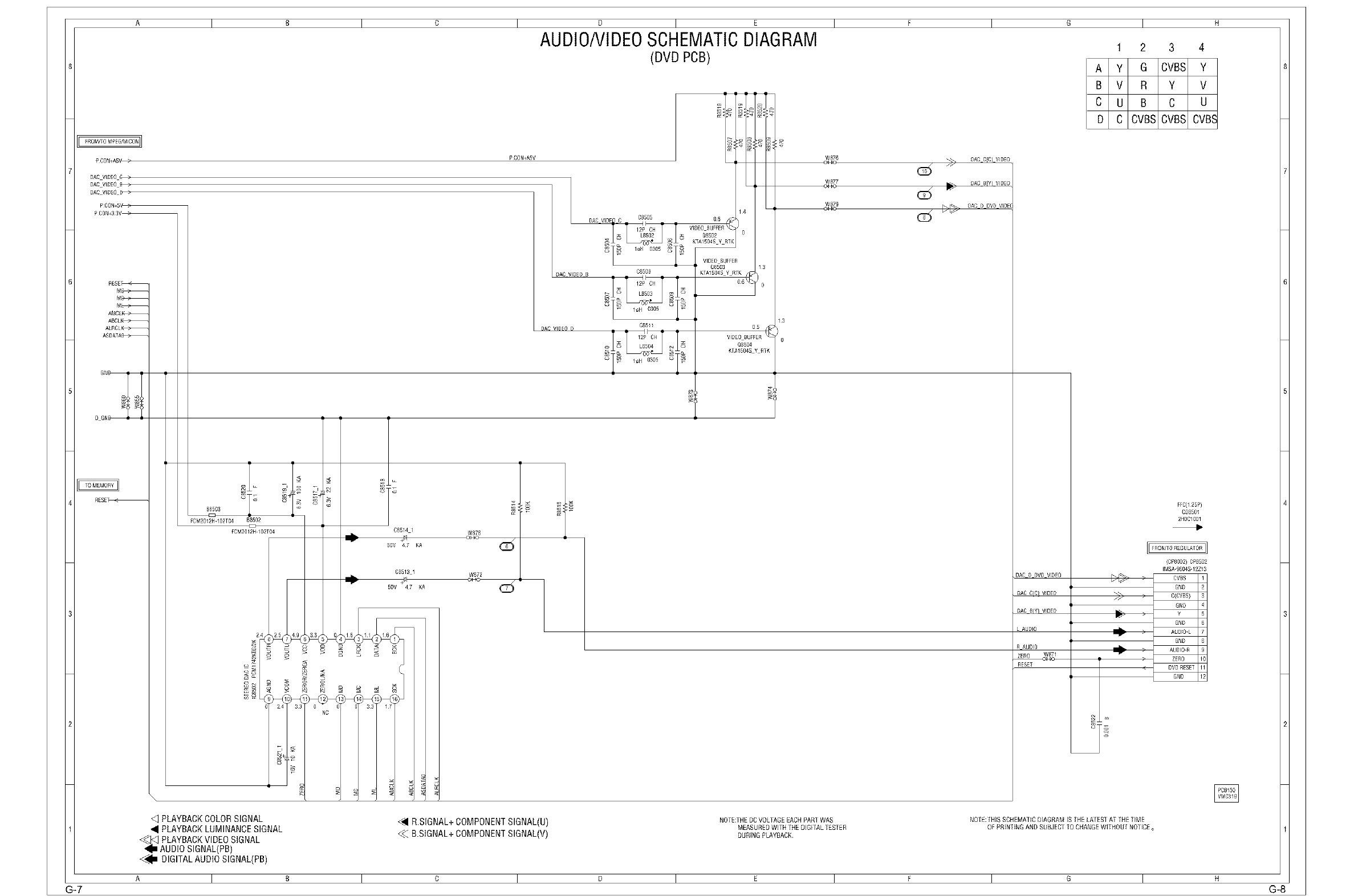
A I B I o I D I E I F I G I
AUDIONIDEOSCHEMATICDIAGRAM
(DVD PCB)
p CON+A5%r >
DAC VIDEO C
DAC VIDEO 0
DAC VIDEO D
PCON+5V
PCON+33V_
RESE_
M_
AMCLF_
ABCL_
ALRCL_
ASDATA_
RESE_
PCON+A5V
DAC VID£O D
--:-:
DAC ViD C8505 0 6 1 4
I_T 12_ 1" vlDOBUFFER
08502 0
° o _ ° KTA1504S Y
VIDEO SUFFER
Q8503
DAC VDEO B 08508 _{i _{TA1504S Y T_{ ? o
I 1211 CH = 0 6 0
C8511
_I _ I_H 0305 _I_ _'TA1504S Y R]
W876 _ DAC C[C VIDE[
W877 DAC B/Y ! VIDE[
o_o
w87_ _-_ DACDDwViDE
13
FCM2012H.1(}2T04 B8502
FCM2012H-102T04
8
C8514
50v 4 7 KA
CS513 1
50v 4 7 KA
W878
ce¢o
W872 DAC D DVD VIDEO
DAC CICI VIDEO
DAC BIY_ VIDEO
L AUDIO
R AUDIO
ZERO W871
RESET
\\
H
1 2 3 4
A Y G CVBS Y
B V R Y V
C U B C U
D C CVBS CVBS CVB8
FFC(I 25P)
CD8501
2HOC1001
(0P8002) 098502
IMSA-9604S-12Z_3
'q PLAYBACKCOLORSIGNAL
• PLAYBACKLUMINANCESIGNAL
<_'_ PLAYBACKVIDEOSIGNAL
_lI AUDIOSIGNAL(PB)
_lI DIGITALAUDIOSIGNAL(PB)
_• R.StGNAL+ COMPONENTSIGNAL(U)
C<_B.SIGNAL+ COMPONENTSIGNAL(V)
NO[E:TH_ DCVOLTAG_ EACH PARI WAS
M£ASUR_D WI[H H_ DIGllAL [_SIER
DURING PLAYBACK¸
NOIE: IHIS SCHEMA[IC DIAGRAM iS [HE LA[ESI AT IHE lIME
OE PRIN] ING AND SUSJEC[ TO CHANGE WITHOUI¸ NOTICEo
A I _ I C I D I E I _ I G I H
G-7 G-8
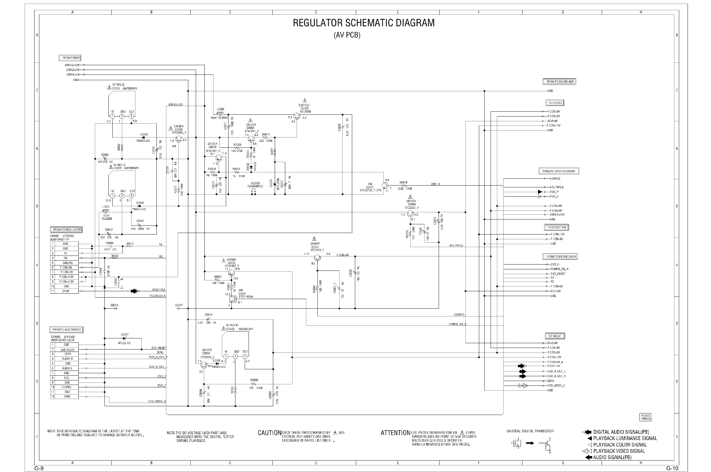
A I B I o I D I E I F I G I H
REGULATORSCHEMATICDIAGRAM
(AV PCB)
UNREG+12V )
UNR£G+SV )
UNREG+_V )
GND
0P8001 (CD8505)
A2001WV211P
GNJ
GNJ
TX z
GNJtM)
PCON+9V _(
PCON+5V
PCON+33V j
PCON+33V
CND
SPD'F
F_OM/TOAUD_ONIDEO] I
CP8002 (CP8502}
IMSA-9604S-12Z14
IN GNO OUT
8__ D3008
III
IN4005-_1C
CND
DVD RESET z
Z£RO
AUDO-R
GND
AUDO-L )
CND
YrC)
GND
CfCV_S)
CND
CV_S
C3005
16V470 YK
16V 470 YK
C3002 W819 TX
W803 RX
,,_lb._ SPDIF-13Z
PCON+5V_
SO01X
_+
D3007
MTZJ56B J
DVbRESE
Z£RO
DVD A OUT
DVD A OUT
DVD
DVD
bVb VDEO
UNREG+12V
Q3006
DRIVER
KTC3203 Y
_ 79_ 80
IOUN TSL0801
o
B
DRIWH I
Q3Olu
1181 I
R3011
IM 1/4w i
Q
33V O_T
03003
_TC4369
DRIV£R
KTA1281Y >
IK 1/4W _ _._
HS3001 _, i_f_
763WAA0157 _ _
KTA1281Y
SW
330c
DTC 14E_A
C3014
63V O0 YK 5V R£G IC
z_1C3002 KIA7_O5API
bRVER
(13009
KTC3209 y
_ _7496 b3005 81 ,_ 49
_ _ 100 1/4W
DR_V[R
03005
KTC3209 Y
119 90 p CON+gV
DVD N
DRIVER
Q3008
KTC3203 Y
AT57VREG
85VRE_
POWER ON t
[E FROM/TO SOUND AMP_
GND
) P CON+gV
) p CON+5V
) AT+56V
PCON+12V
GND
I FROM/TO VIF/SIFICNROMA 1
85VREG
( AT57VREG
_ DVD Y
_ DVD C
P CON+5V
) P CON+gV
NREG+ 2V
CND
p PCON+12V
PCON+5V
OND
< DVD H
( POWER ON H
( DVD RES[T
( RX
) TX
) PCON+5V
) AT+56V
OND
AT+56V
p P CON+OV
) P CON+5V
PCON+I2V
) PCON+5V A
_.. ) SPDI_q34
) DVD A OUT L
,,_ ) DVD A OUT R
ZERO
_ND
NOIE: fillS SCHEMAHC DIAGRAM IS INE LA[ESI A[INE lIME NOTE: f HE DO VOL rAGE EACH PAR[ WAS CAUTIONsINCE[H_SE PARIS MARKED BY Z_ ARE ATTENTION:LESPIECES REPANEES PAR UN Z_ E[ANf CAU]ION: DIGITAL f RANSISTOR _11 DiGiTAL AUDIO StGNAL(PB)
1 OE PRIN lING AND SU_JEC [ fO CHANGE WIINOUI NO[ICE. M£ASURED WI1H INE DIGIf A£ IESfER CRINCAL FOR SAFE [Y,USE ONES DANG£RENS£S AN PONf DE VUE S£CUNI[E • PLAYBACKLUMINANCESIGNAL 1
DURING PLAYBACK DESCRIbeD IN PARIS LIS[ ONLY o N:UIILISER QUE C_LLS D_CRIf ES _vv_
DANS LA NOMENCLAfURE DES PIECES_ _ <] PLAYBACKCOLORSIGNAL
q_'_q PLAYBACKVIDEOSIGNAL
AUDIO SIGNAL(PB)
A I _ I C I O I E I F I _ I H
G_9 G_IO
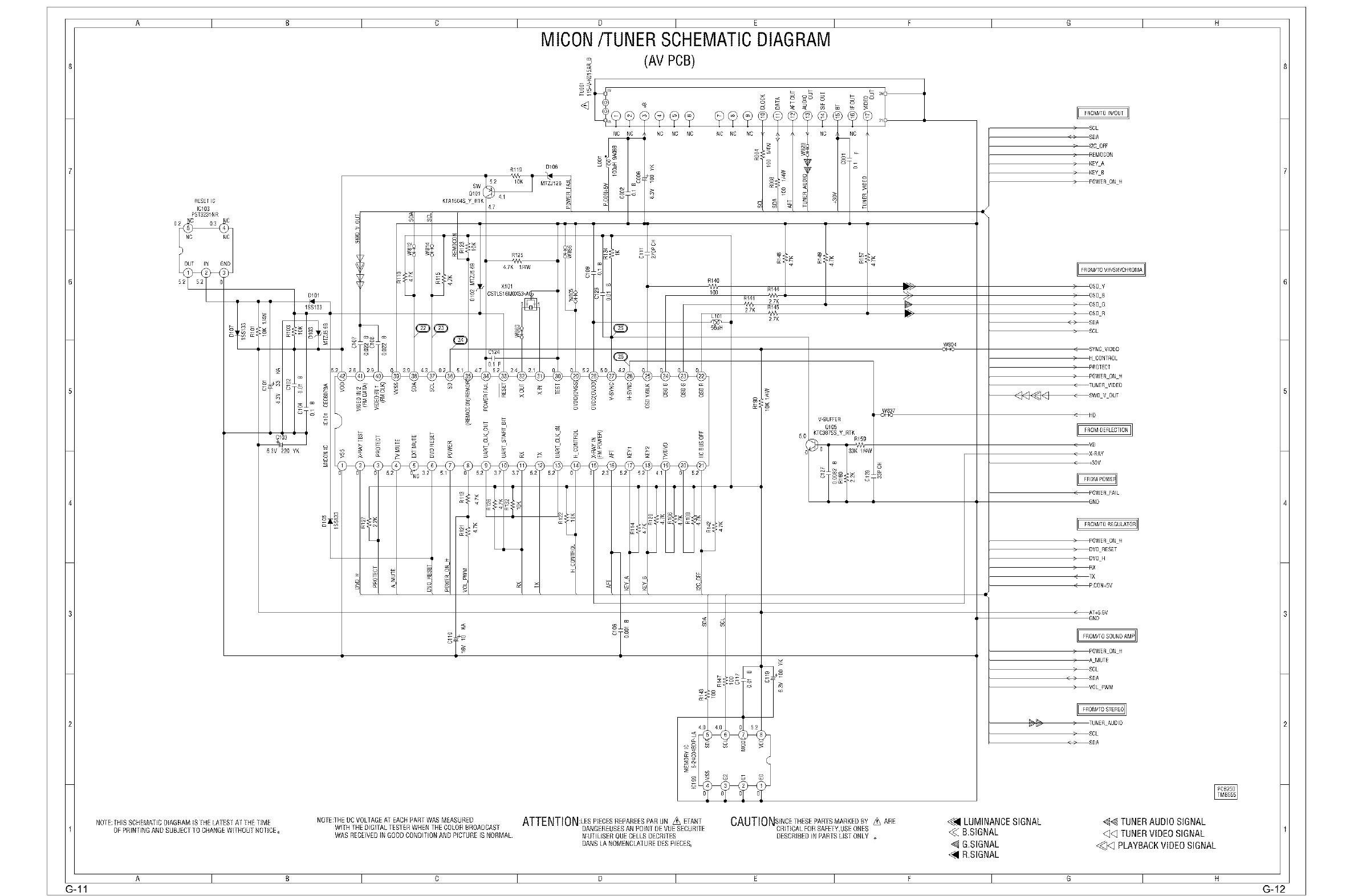
A I B 0 I F I G I a
RESET IC
IC103
PST8231NR
D101
_E 2
63V 220
D I E I
MICON/TUNERSCHEMATICDIAGRAM
(AV PCB)
R119 D106
'52 10K
O101 I
KTA1504S Y RTK
I II
_ R125 1_
X101
_ CSTLS16MOX53-A _!
_24
0IF
NO NO NO NC NO NC NC
oco 2, _o
, NC _NC ,_
_1 _ I
Y
_4
/i/i/-_/i
>
>
>
>
[E FROM/TO IN/OUT 1
SCL
SDA
2C OFF
RE_OCON
KEY A
KEY B
POWER ON H
[E
[E
W837
V-BUFFER
Q105
50 KTC3875S Y RTK
OSD Y
OSD B
OSD G
OSD R
SDA
SCL
SYNC V_DEO
I1 CONTROL
PROTECT
POWER ON H
TUNER VIDEO
SWD V OUT
ItD
FROM DEFLECTION
VD
;(-RAY
_SOV
POWER FAIL
GND
FROM/TOREGULATOR 1
POWER ON H
DVD RESET
DVD H
RX
TX
PCON+5V
AT+56V
GND
POWER 011 H
A MUTE
SCL
< ) SDA
VOL PWM
_- TUNER AUDIO
> SCL
SDA
NO[E: [HIS SCNEMAHC DIAGRAM IS IHE LAIES[ Af THE TIME
OF PN]NHNG AND SUBJECT10 CHANG£ WITHOUT NOflCE o
NO1E:fNE DC VOLTAGEA[ EACH PANEWAS M_ASURED
WITH THE DIGITAL TESTER WNEN [NE COLORDNOADCASf
WAS NEC_IWD IN GOOD CONDITION ANN PICTURE IS NORMAL¸
ATTENTION:LESPIECESNEPAN_ES PAN NN _ ELAN[
DANC_NESS_S AN POIN[ DE NUNS_CURI f E
N'UIILIS£N QU_ CELLS N£CNI[ES
DANS LA NOM_NCLA1UNE D_S PIECES. DESCRIBED IN PARES LIST ONLY o
_1 LUMINANCESIGNAL
_< B.SIGNAL
'_ G.SIGNAL
_1 R.SIGNAL
4<_ TUNERAUDIO SIGNAL
'_'_ TUNERVIDEO SIGNAL
_'_'_ PLAYBACKVIDEO SIGNAL
A I _ I o I D I E I _ I G I H
G-11 G-12
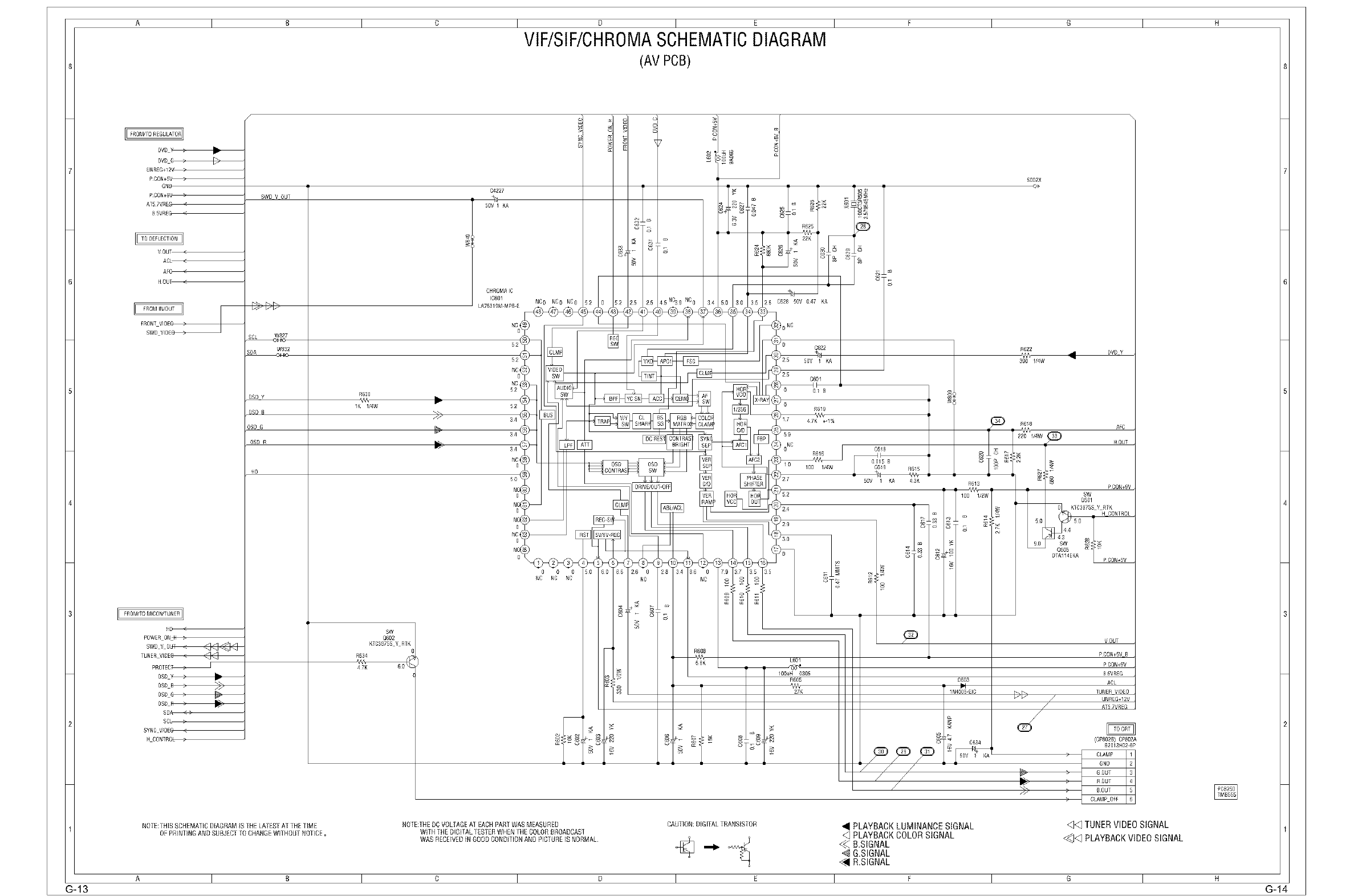
A I B I o I D I E I F I G I H
VIF/SIF/CHROMASCHEMATICDIAGRAM
(AV PCB)
DVD y)
DVD C
NREG+12V )
P CON+5V )
GN£
P CON+gV )
AT5 7VREC
8 5VREC
VOUT
ACL (
AFC
HOUT (
FRONTVIDEO
SWD VIDE_
POWER ON II
©
/i/i/_1/i
SWD V OUT < _ _
TUNERVID:O < _
PROTEC_
OSD Y ;_.-
OSD C _
SDA < )
SCL )
SYNC VIDEO
N CONTROL
SWD V OUT
0SD Y
0SD B
OSD G
OS# R
HD
R630
IK IRW
SW
Q602
KTC3875S YRTK
C4227
50V 1 KA
CROMA IC
IC601
LA7631£M-MPB-[ NCO NCO NCo
i °
o<
R6
22
SO02X
C628 50V 047
NC
C622
50V _
C601
01 B
R619
4 7K +.1%
C618
R616 II
I 0015 B100 I/4W _9 R615
_OV I _ 4 3_
• DVD Y
R618
R613
AFC
_O_T
PCON+_
SW
Q601
R605
27K
D603
DTA114E_
v OUT
PCON+5V B
PCON+gv
85VREG
ACL
TUNER VIDEO
UNREG+I2V
AT57VREG
fCPS02B) 0_802A
B2013H02 6P
NO[E: [HIS SCHEMA] IC DIAGRAM IS filE LA]ES f Af THE HME
OF PRINlING AND SUBJLCT 10 CHANGL WITHOUT NOflCE.
NOfE:[HE DC VOL[AGE AI EACH PAR[ WAS MEASURED
WITH TRL DIGITAL TLS [LR WHLN 1HE COLOR13ROADCAS[¸
WAS RLCEIVED IN GOOD CONDITION AND PIC[URL IS NORMAL¸
CAU]ION: DIGITAL TRANS[S[OR • PLAYBACKLUMINANCESIGNAL
<] PLAYBACKCOLORSIGNAL
_< &SIGNAL
G.SIGNAL
_• R.SIGNAL
4_ TUNERVIDEOSIGNAL
_<] PLAYBACKVIDEOSIGNAL
A I _ I o I D I E I _ I G I H
G_13 G_14
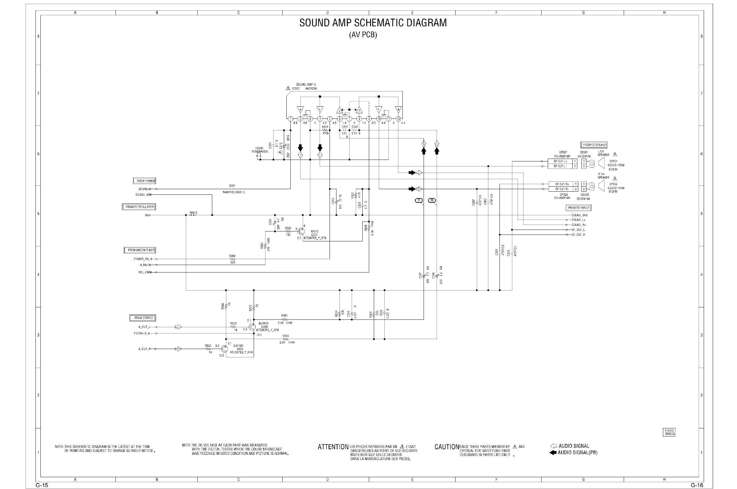
A I B I 0 I D I E I F I G I H
SOUNDAMP SCHEMATICDIAGRAM
(AV PCB)
SOUND AM9 IC
Z_ IC302 AN7522N
if
SOUND_B
SOUND CND
_FROMT[OREGULATOR_
W813
GND oe_o
FROM MICON/TUNER_
POWER ON II
A MUT£ )
VOL PWM >
A OUT L )
P CON+2 g
A OUT R _
B301
W4BRH35X6X10
R302
_,N_,
_RK
R301
R_ ) KBid_iqS y RT _ _K_/'/4W
120 R303
',M,
2 2K /4W
<*
_Z > o'
o o>
C_301
TID-X02P-M1
CD301 LCN
CU12414A SPEAKER ,_
SP351
SGO4D11BNA
8 OHM
RCH
SPEAKER _
SP352
SGO4DIISNA
8 OHM
NO[E: [NIS SCREMAI[C DIAGRAM IS filE LA]ES f AI THE lIME
OF PRIN lING AND SUBJECTIO CNANG£ WI] HOUT NOflC_.
NOlO:f HE DC VOLTAGE Af EACH PAR[ WAS M£ASURED
WITH THE DIGITAL TES]_R WREN [HE COLOR RROADCASf
WAS RECEIWD IN GOOD CONDITION AND PICfURE IS NORMAL¸ N:U [[L[SER QUE CELLS DECR[TES
DANS LA NOMENCLAIUR£ DES PI£CES_
DESCRIB£D IN PARRS LIST ONLY o
_:z AUDIOSIGNAL
_lmAUDIOSIGNAL(PB)
A I B I 0 I D I E I F I G I H
G-15 G-16
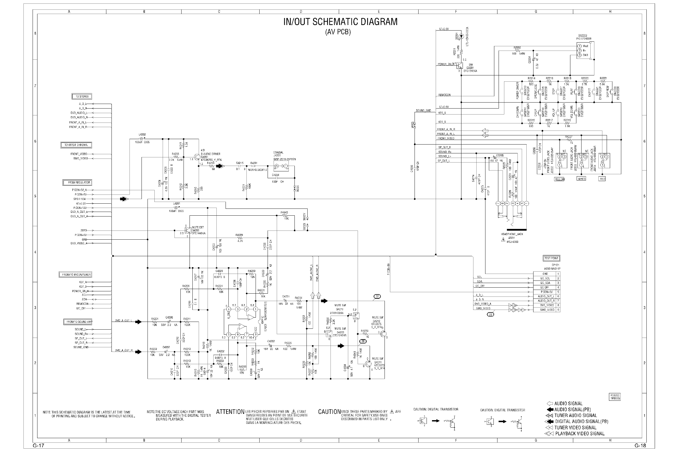
A I B I o I D I E I F I G I H
IN/OUTSCHEMATICDIAGRAM
(AV PCB)
AOL .
AO -
DVD AUDO
DVD AUDO
FRONT A N L .
FRONT A N
[E TO VIF/S FCHROMA
fRONT VDE_
SWD VDE_
FROMREGULATOR_
PCON+SVA )
P CON+5V )
SPD f. 34 ml_-
L4202
IOOUH 0305
49
R4205 D AUDIO DRIVER COAX AL
042(}1 J4201
[2K 1/4W KTC3875S Y RTK MSP 251V-OSPBSN
g R4216 C4215 B4201
SOUND GND
i
<3
AT+56V
a_
SW
02201
DTC124EKA
REMOCON
AT+56V
_EY A
_EY B
FRONT A IN R
FRONT A IN L
FRONT VIDEO
SP OUT R
SOUND R+
SOUND L+
SP OUT L
m
R2202
100 I/4W
R2214
820
0S2202
PIC-37243SR
R2216 R2218 R2220 R2221
1 5K
AT+56V_
P CON+12V
DVD A OUT
DVD A OUT
ZERO )
PCON+9_
GN_
DVD VIDEO_
KEY
KEY_
POWER ON_
SC_
SD_
REMOC
12C OFF_
I FROM/TOSOUNDAM_ DVD A OUT L
SOUND_
SOUND_
Sp OUT E_<
SP OUT_
SOUND G_
DVD A OUT R
MUTESW
Q4212
KTC3875
S Y RTKO
N
EADPHONE JACK
SWD VIDEO
CPI01
A2OO1WV2 9P
AUDIO SIGNAL
NOFE: IRIS SCR_MAHC DIAGRAM IS IH_ LA[ESI AI 1HE lIME NOIE:[H£ DC VOL[AGE EACH PAR[ WAS CAUTIONslNc£ [RES£PAR[S MARKED13Y_ARE CAU [ION: DIGI [ALI RANSIS [OR CAN l ION: D[GIIAL [RANSIS fOR _lI AUDIO SIGNAL(PB)
1 Of PRIN lING AND SURJEC[ lO CHANGE WlfNOUf NO [IC_ oMEASURED WlfN [HE DIGIfAL fESteR CRH [CAL _OR SAFE[Y,US_ ONES _ _ TUNERAUDIO SIGNAL 1
DURING PLAYBACK N:Ur[L[SER QUE CELLS DECR[I£S DESCRIBED iN PARRS LISf ONLY ._4,¢_
DANS LA NOMENCEAIUR£ DES PIECES_ _ _ _l I DIGITAL AUDIO SIGNAL(PB)
qqTUNERVIDEO SIGNAL
_] PLAYBACKVIDEO SIGNAL
A I _ I c I a I E I F I _ I H
G_17 G-18
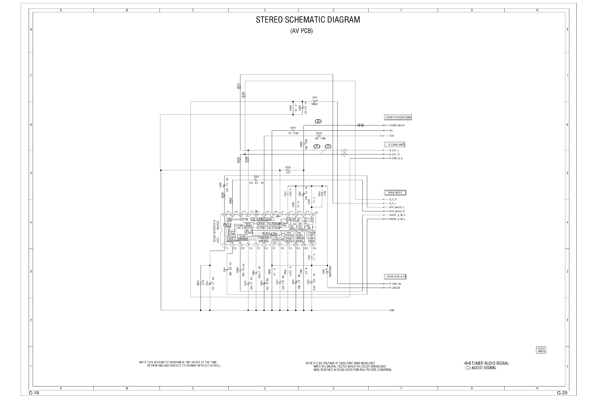
A I B I o I D I E I F I G I H
STEREOSCHEMATICDIAGRAM
(AV PCB)
L904
IO0_H
R912
10(} _/4W
/
4
_;_ ( TUNER AUDIO
( SCL
( ) SDA
_ _ AOUTL
) AOUTR
_ P CON+12 A
( A0R
A0L
_DVDAUDIOL
_DVDAUDIOR
<FRONT AIN R
_FRONT AIN L
_ P CON+12V
< P CON+5V
GND
NO[_:THIS SCH£MA] ECDEAGRAMIS fRE LATESf AI IRE IIM£
OF PR[NI¸INGAND SUBJECf [0 CHANGEW[]ROUT NO[ICE o NOfEJHE DC VOLIAGE AI EACH PAR1 WAS MEASURED
WITH ]R_ DIGITAL [ES [ER WHEN 1HE COLOR 13ROADCAS]¸
WAS R_CEIVED IN GOOD CONDITION AND PIC[UR_ IS NORMAL¸
'_< TUNER AUDIO SIGNAL
_:z AUDIO SIGNAL
A I B I 0 I D I E I F I G I H
G-19 G-20
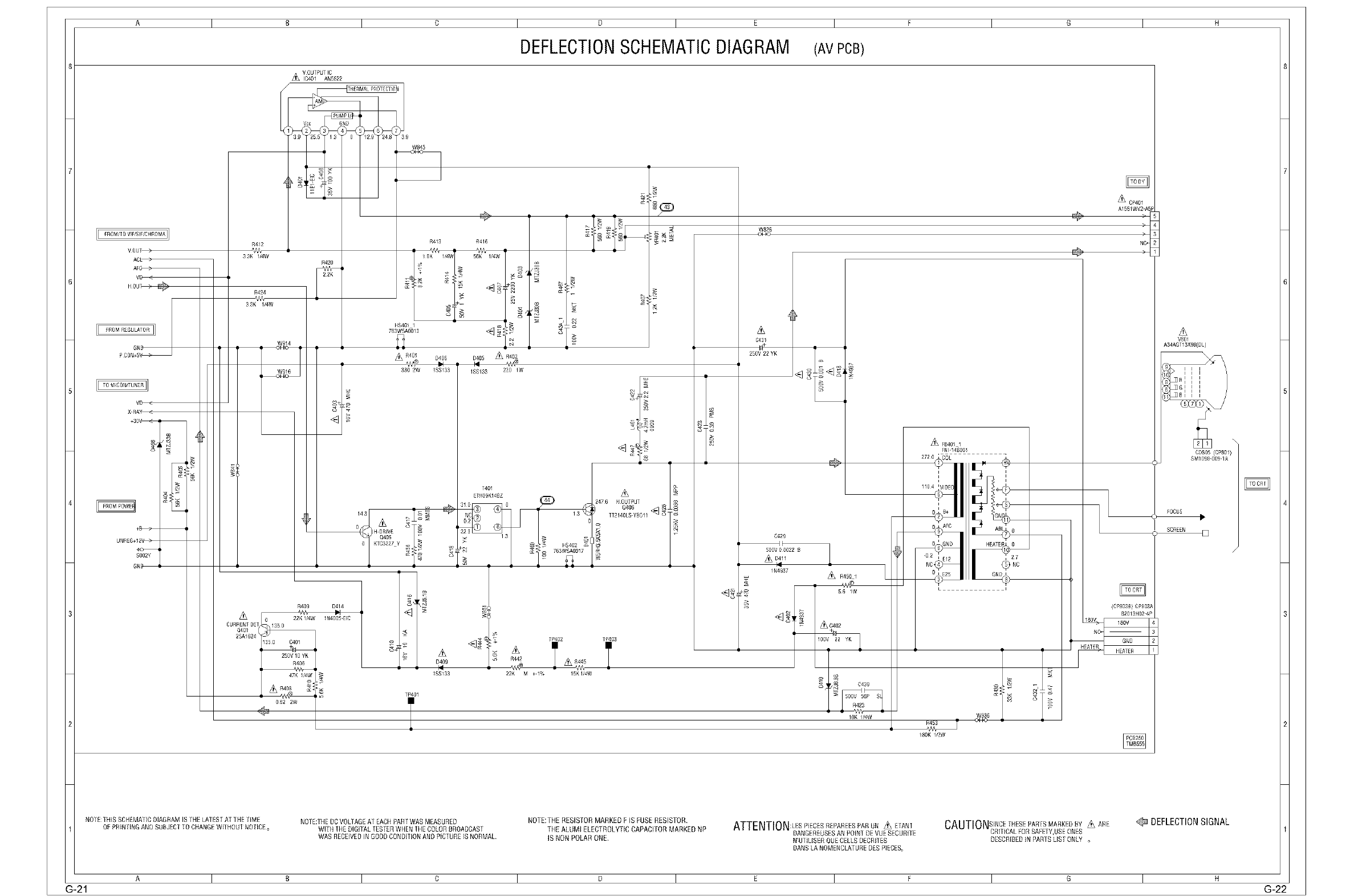
A I B I D I D I E I F I G I N
DEFLECTIONSCHEMATICDIAGRAM (AVPCB)
8 8
FROM/TO V HS F/C ROMA]]
VOUT )
ACL )
AF_
R412
33K 1/4W
R424
V_
3 3K 1/4W
W914
W916
R420
2 2K
I
R409 D414
_N4OOS-EIC
350 C401
250V10YK
R406 t
47K _/4W
082 2W
330 2W
o
D409
_SS133
TP401
_R402
9406 _f_
_SS133 ISS133 220 IW
22K M +-1%
TP402 TP403
T
15_1/4W
_:_
_- _
H OUTPUT _
TT2140LS-YSCH
_6
42
C431
_+ _
250V 22 YK _
C429
/
500V 0 0022 B |
IN4937
_ _ R450 _
>
g? _ C439
500V 56P S
R423
1OK /4W
Z_FB401 1
FM-14EO01
R453 _
_80K 1/9W
AI561WV2ASF
o
0
(C9803_}C_803
B2013HO24P
z_
V801
A34AGT13X98(_L)
SMIO98-OO9-1A
FOCUS
NOTE:fills SCHEMATIC DIAGRAM IS IHE LAFESI AT IHE [[ME
DE PRINTING AND SUR,_EC[ TO CHANGEWITHOUT NOTICE o NO] E:THE DC VOL[AGE A[ EACHPARr WAS MEASURED
WITH 1HE DIGIfAL ¸[ESTERWREN 1HE COLOR _3ROADCAS[
WAS RECEIVEDIN GOOD CDNDIliON AND PICTURE IS NORMAL¸
NOTE:THERESISTORMARKEDF IS FUSERESISTOR
THE ALUMi ELECTROLYTICCAPACIfOR MARKEDNP
IS NONPOLARONE N'U]ILISER QUE CELLS DECRUES
DANS LA NOMENCLAI URE DES PIECES_
DESCRIBED IN PAR [S MS [ ONLY o
DEFLECTIONSIGNAL
A I B I D I D I E I _ I G I N
G-21 G-22
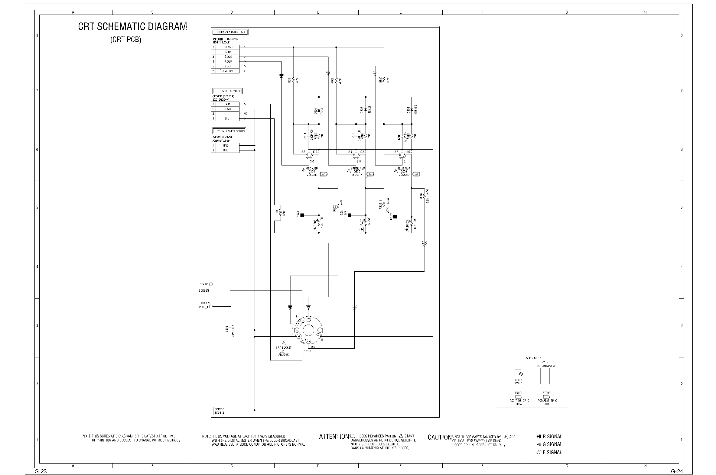
A I B I o I D I E I F I G I H
CRTSCHEMATICDIAGRAM
(CRT PCB)
FOCUS
SCREEN
SCR£EN
8P806 1
CPS02B (CPS02A)
B2013H026p
CPS03B(CPS03A)
B2013N02-4P
CPS01(CDS05}
A2361WV2-2P
_>
2SC4217 2SC4217
z_
CRTSOCKET
J801 1
ISMS01S ACC£SSORY
BL001
HpN-01
TMI01
TOT201N09160
BT001 BT002
D D
R03(AB)[2P G R03(AS}£2P G
UM4 UM4
NO[£:THIS SCHLMA] IC DIAGRAM IS file LATESf AI ]HE [IML
OF PRINTING AND SUBJECf [0 CRANGL WITHOUT NO[ICL o
NOfE:[HE DC VOL[AGE AT EACHPAR[ WAS MEASURED
WI[H 1NL DIGIIAL [LSILR WHLN IHL COLOR 8ROADCAS]
WAS RLCMVED iN GOODCONDIIION AND PIC[UR£ iS NORMAL
ATTENTIONLESPILBESRLr_ARLESPARBNz_ELAN[
DANGLREBSLS AN POINI DE VUE SLCURIIE
N:UHLISER QU£ BELLS DLCRRES
BANS LA NOMLNCLAfURE DES PIECL_
CAUT ONSINCLTHESLPARISMARNLD _Y _ ARE _'_ R.SIGNAL
CRIIICAEFORSAFLIY,USEONLS
DESCRIBEDiN PARISLID[ ONLY . _ &SIGNAL
_ B.SIGNAL
A I B I c I D I E I F I G I H
G-23 G-24
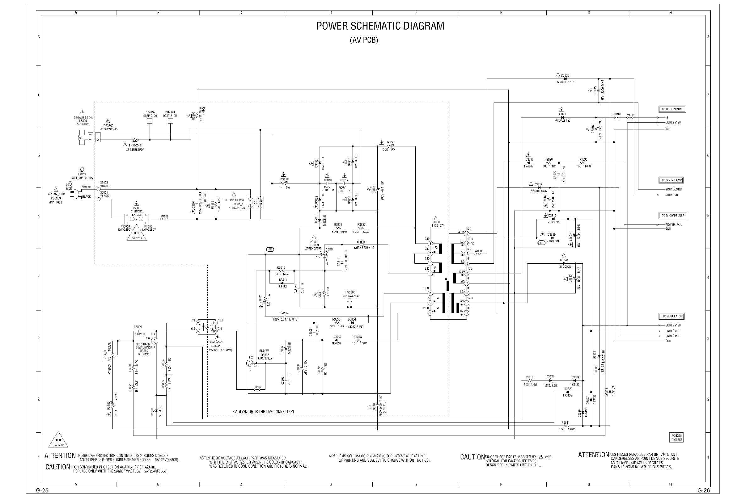
A I B I o I D I E I F I G I H
POWERSCHEMATICDIAGRAM
(AV PCB)
F
8RI40031 ,
Q I
L3803
,$3802
CP380(}
PH3800 PH3801
003P-2100 O03P 2100 _1_
!!,
_ TH3800 2
ZPB45BL3ROA
C3809
IFE[D _ACK
IC3800
PS2561LI I-VfW)
w
C3810 C3812
,, T, T
50(}V 500V
iL
3826 R3827
_W_VV _,
12M 1/4W 12M /4W
z_
POWER
Q3803
STP5NCSOFP
B3800
1_240 _ _ W5RH3 5X5X1 0
R3_16 _T_
680 _/4W '
D3811
ISS133 _ _-
'_]_ : _ 763WAA0227
C3807 ID
/ lOOV O0 7 MMTS R_
_ _ N4937 10 /2W
Q3802
63 kTC3203 Y _
m _ _ N
i ,
CAUFION: _ IS[HE LIVE CONNECflON
,_ R3828
_,NV¢
(}22 _W
o>
o
T3800
81291(}74
,_3823
SB340L'6737 _
D3821
RU2AM'£1C
D3818 R3829 R3830
_N4937 _00 1/4W _ IK 1/4W
>
,_ D3817
D382(}
R3813 D3831 b3802 _:_
00 1/4W MTZJ3 9B ISS133
b3822
1-i
ISS133
R3831
100 1/4W
_T
o _B
UNR£G+12V
GND
SOUND GND
_SOUND+B
POWER FAIL
GND
UNR£G+12V
UNR£G+RV
UNR£G+SV
-GND
1 ATTENTION :POURUN_PROFECUONCONTINUELESRISQU_SD1NCEIE
N'UflLIS_RQUEDESFUSIBLED_MEMEfYPE 5A125V(F3800)
CAUTION :mR CONRNUEDPROfECIIONAGAINSf FIREHAZARD,
R£PLAC£ONLYWI[H IHESAME[YPE_USE 5A125V{F3800)
NO[£:TRE DC VOLTAGEA] EACH PAR[ WAS M£ASUR_D
WiTH IRE DIGIfAL TESTERWHeN TH_ COLOR BROADCAST
WAS RECEIVEDIN GOODCONDITION AND PICIUR_ IS NORMAL¸
NO[E:THIS SCHEMA]IC DIAGRAM IS filE LA]_S f AI THE [IM_
OF PRINTING AND SUBJECT [0 CRANG_ WI] HOUF NOTIC_ o CAUTIONsINcE [H_SEPARISMARKEDRY_ AR_
CRIflCAL FORSAFE[Y,USEONES
DESCRI£_DIN PARIS LIS[ ONLY o N'UIIUS£RQU_CELLSDECRIIES
DANSLANOMENCLAIUR£D_SPIECES_
A I _ I o I D I E I F I G I H
G-25 G-26
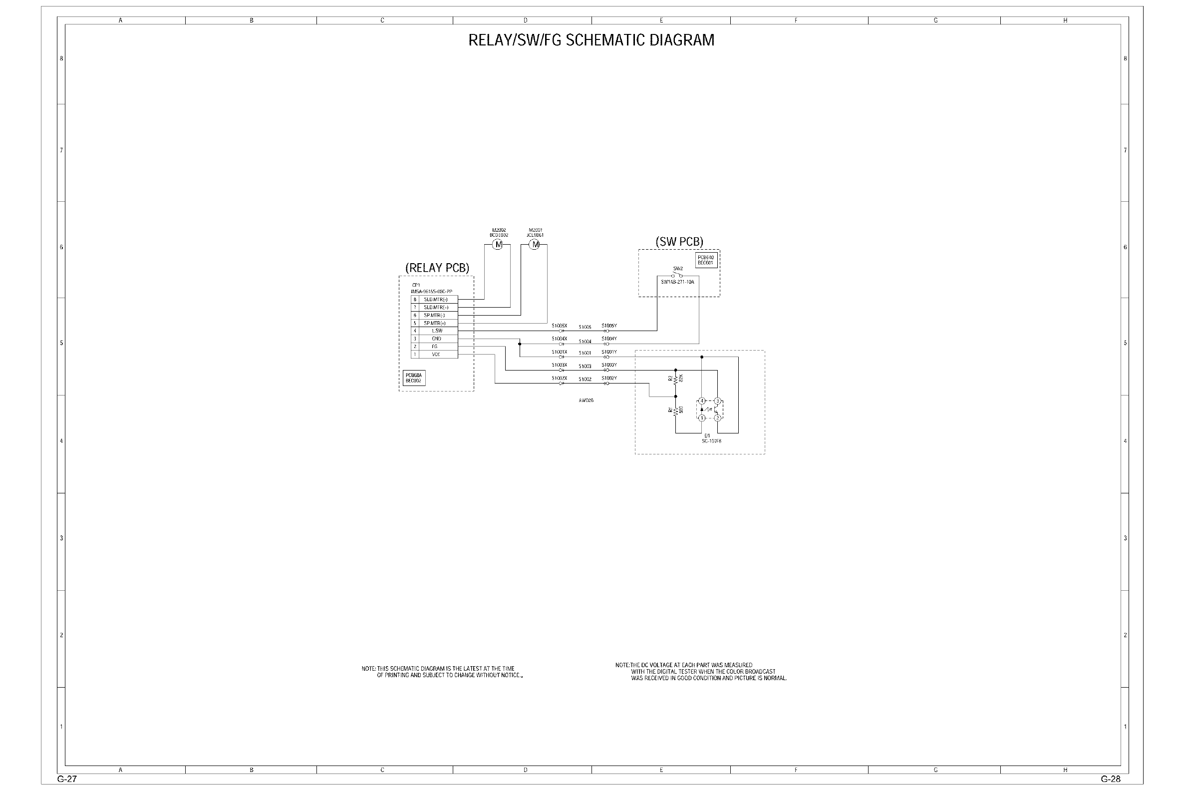
A I B I c I D I E I F I G I H
RELAY/SW/FG SCHEMATICDIAGRAM
M2002 M200T
_CD3B02 JCLgB61 (SW PCB)
SW2
$W1A_2J1 _0A
S_003X S_003 S1OO3Y
i
S_002X S_002 S1OO2Y i
AWD28
D_
SG 107£6
NOTE:THIS SCHEMAI ]C DIAGRAM IS THE LATEST AI THE T_ME
Or PRiNTiNG AND SUBJECT10 CHANGEWITHOUI¸NOTICE o
NOTE:I HE DC VOLTAGE AI EACH PART WAS MEASURED
WiTH TIIE DIGit AL TESTERWHEN TIIE COLOR BROADCAST
WAS REC_[WD IN GOODCONDITION AND PICTURE IS NORMAL¸
P I B I c I D I E I F I G I H
G-27 G-28
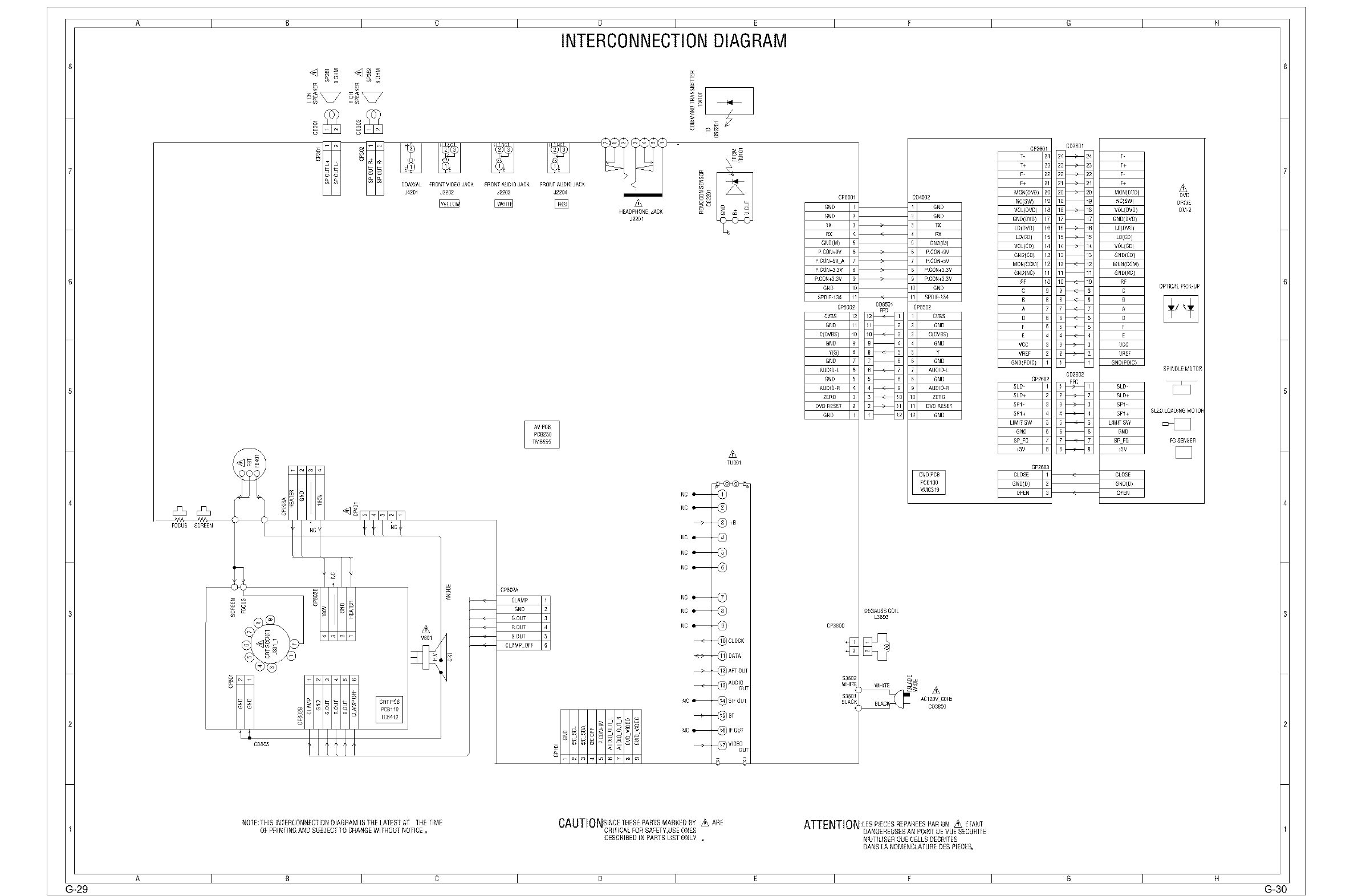
A I B I o I D I E I F I G I H
INTERCONNECTIONDIAGRAM
FOCUS SCREEN
0D805
L_ L_
COAX AL FRONTVI0£0 JACK FRONTA D 0 JACK FRONT AUDIO JACK
J4201 J2202 J22(}3 J2204
,&
HEADPHONE JACK
J2201
>S
o:
_ CP8(}01
° GND T
: GND
TX T
RX T
GND(M) 5
P OON+gV T
P OON+5V A 7
p CON+3 3V
p CON+33V 9
GND 19
SPD]Fq34 11
CP8002
CVBS 12
GND 11
C{CVBS) 19
GND 9
Y(G) T
GND
AUDIO_
GND 5
AUDIO4_
ZERO
DVD RESET
GND T
o
NO
NC
NC
NC
NC
NO o,
NC o,
NC
NC
NC
TUO01
xp
C)
Xo
x_
_) CLOCK
_DATA
_) AFT OUT
_)S FOUT
_BT
_IF OT
_ VIDEOIjT
CP3800
CD8501
FFC
D[GA SS COL
L380(}
C926(}1 24
23
22
21
]VD) 2(}
CD4(}02 ¢_) 19
_ VD} 18
i Vb ) 17
b) 16
)) 15
O) 14
_D} 13
OM) 12
JC} 11
1(}
10
CP8502 i
Cv_s
GND
c(cvss)
GND
5 _ F 2
GND
7 _u#O-L
GND _CP2602
19 zero i
11 DVI?R£SET
12 _B 4
°
AC120V 60Hz
CD3800
]D2601
MON(DVD) _
NC(SW) DRIVE
_ VOL(DVD) DM-2
GND(DVD)
_ LD(DVD)
_ LD{CD}
_ VOL{CD)
GND(CD}
MON(COM)
_ OPTICAL pIC_-Up
_ Vl;4: i
)D2602
FFC SLD-
SLD+
SPP
Sp_+ SLEDLOADINGMOTOF
LIMIT SW L_
GND
____ Sp FG FGSENSER
CLOSE
__GND{D)
NOfE: [HiS INI£RCONN£CfION DIAGRAM iS filE LATES[ A] IHE tiME
OF PRINTING AND SUSJ£C [ 10 CHANGE WI f NOU]¸NOTICE o CAUTIONSINCETNESE_'ANrS_AONEO@Y_ ARE
CNN ICAL FOR SAFE f Y,USE ONES
DESCRIBED iN PARIS LIS[ ONLY . N:UHLISEROU£CELLSD_CRI:ES
DANSLANOM_NCLAfUREDESPIECES.
A I _ I 0 I D I E I _ I G I H
G-29 G-30
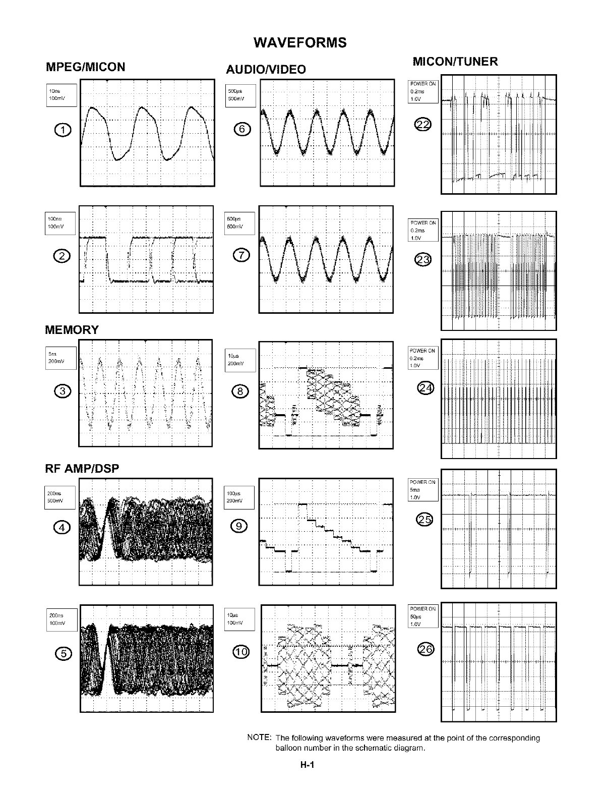
MPEG/MICON
WAVEFORMS
AUDIO/VIDEO
®
MICON/TUNER
I
®
.... iiiii
.... i i
®
T
@
MEMORY
®
RF AMP/DSP
@
®
I _ogs I
12oomv I
_ i_ _i_ i _i _i _ i-
_........._...._,._.... • •..
® _._ _.:<%__ :
u
®................. ;.i__i_.J .............. i.¸_
i
.,... _,_,....,... _ _.;....,.. _ ..,....;.__ ...,....,._; _,,_
@.. :_ .,6,_i,:.}._:;_, :.. :. _.;:_ ,._'_
-_=--_:-_:--.:_:_:[:;;----!.--_----_ _}:_i.,_.L
.., ,,_ ........ _......... ,. _ ..... ,_
:8
_.. !_!,_.%,_,.._.': ::. "4... '_:, ,.._
@
@
@
NOTE: The following waveforms were measured at the point of the corresponding
balloon number in the schematic diagram.
H-1
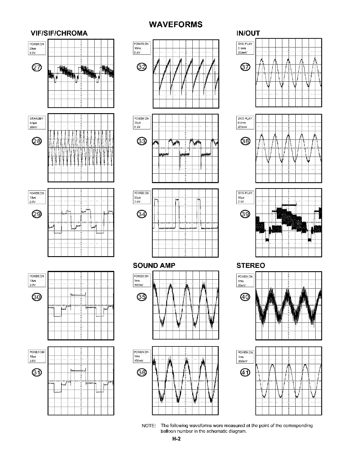
VIF/SIF/CHROMA
@
WAVEFORMS
IN/OUT
eft_,_
l
J \ \
@/Yi<
<ft
\ \
_7 L
_/::<i¸¸
\ \
@
SOUND AMP
I
i
STEREO
@@ 7i,:........._........
NOTE: The following waveforms wore m,_asurod at tha po#_t of the oorrespo[_ding
balloon numbar in the schematic diagram.
H-2
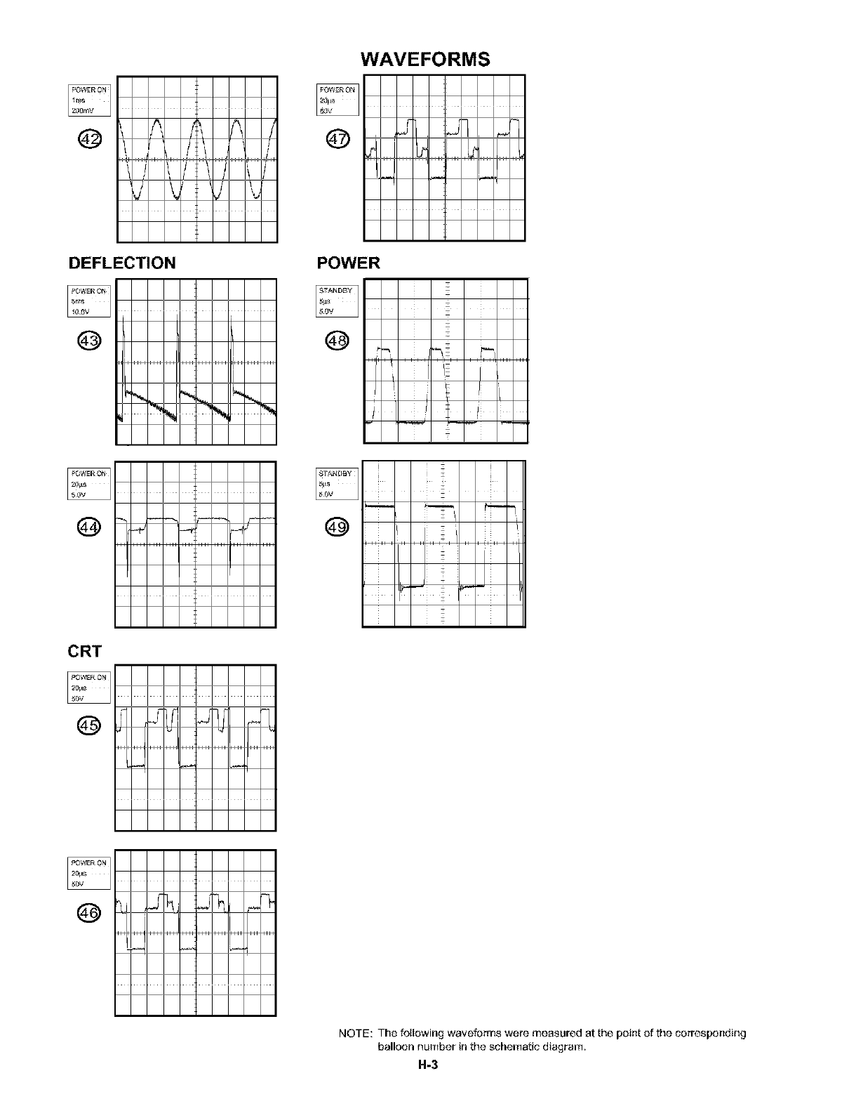
@
DEFLECTION
IlIl_
.... I_H_"HHIHHIHHHL_H
CRT
©
WAVEFORMS
i
POWER
@
i i i Z i i i
"_ _ _F '_
@ii -'_
@
H+ _
NOTE: The following waveforms were m,_asur_d at tha poi[_t of the corresponding
balloon nurt_bJr in th_ schomatio dia,qrar_.
H-3
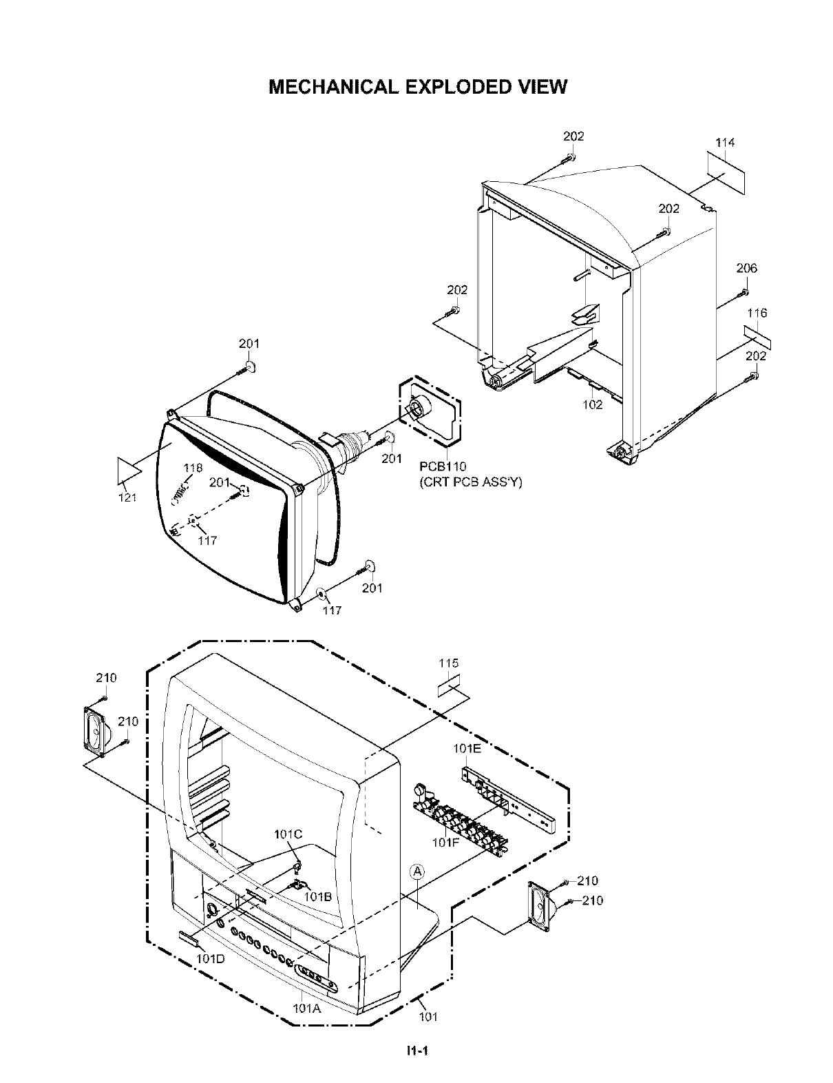
MECHANICAL EXPLODED VIEW
202 114
201
202
206
116
202
102
121
201 PCB110
(CRT PCB ASS'Y)
201
117
210
115
I
i
i
i
It-1
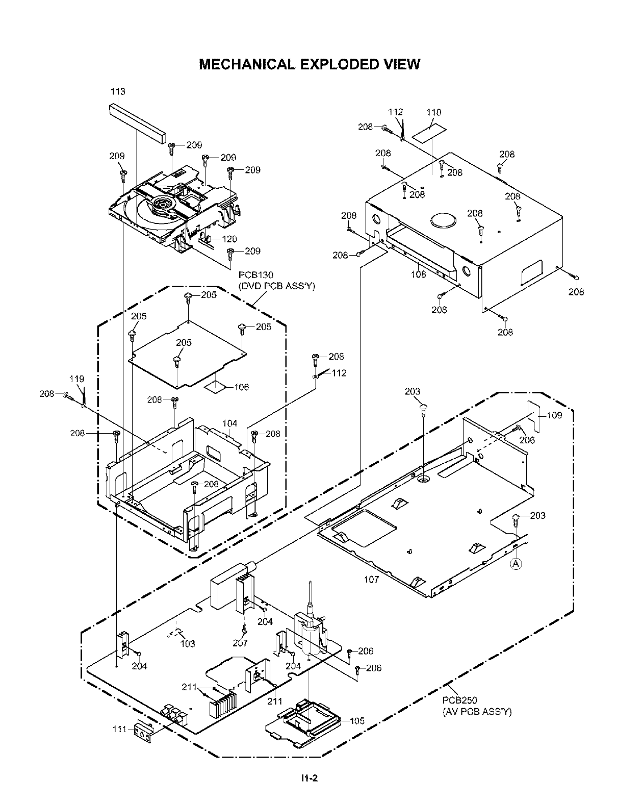
MECHANICAL EXPLODED VIEW
113
209
112
208_
208
110
2O8
i
i
i
L
103
204
211
111
20;
208 0 208
PCB130
(DVD PCB ASS'Y)
-/
203
107
108
208
208
206
204
207
211 _" PCB250
J" (AV PCB ASS'Y)
208
1t-2
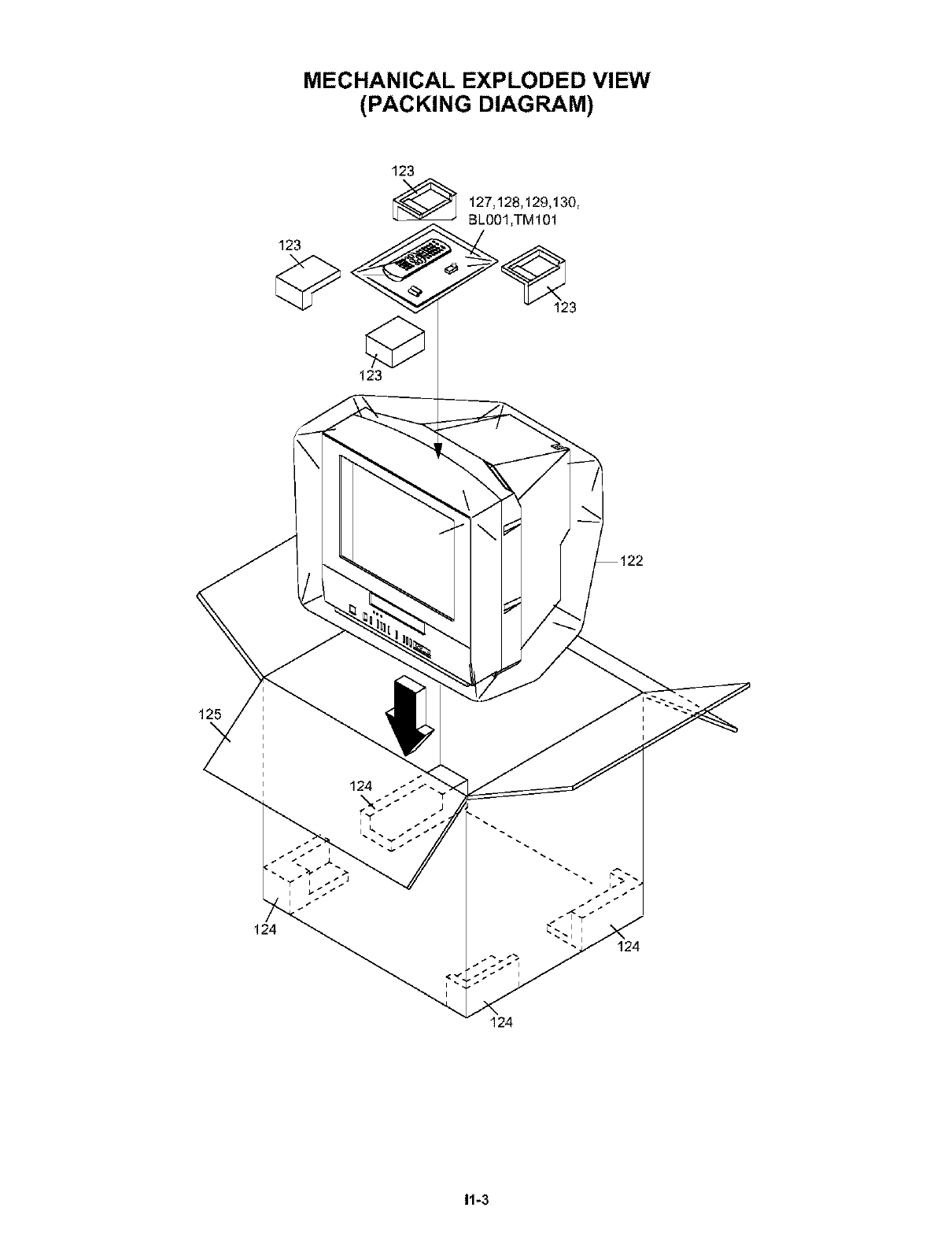
MECHANICAL EXPLODED VIEW
(PACKING DIAGRAM)
123
123
_ 127,128,129,130,
BLOO1,TMI01
123
123
125
\
124
124
124
11-3
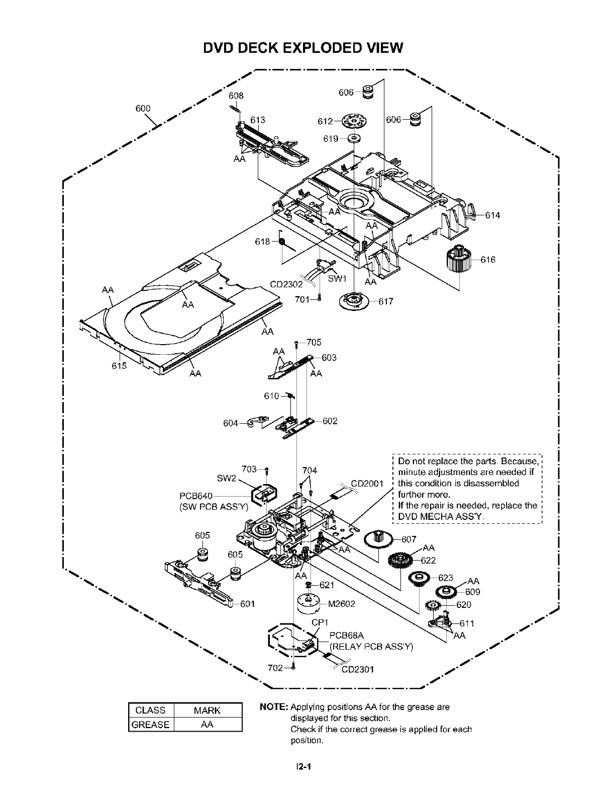
DVD DECK EXPLODED VIEW
613
AA
615
(SW
605
AA
6107
705
_603
AA
_602
704
SW2 _ CD2001
Do not replace the parts, Because, ',
i
minute adjustments are needed if ,
i
this condition is disassembled
further more. i
If the repair is needed, replace the ',
i
i
, DVD MECHAASS'Y,
• .............................
CLASS MARK
GREASE AA
NOTE: Applying positions AA for the grease are
displayed for this section.
Check if the correct grease is applied for each
position.
t2-1
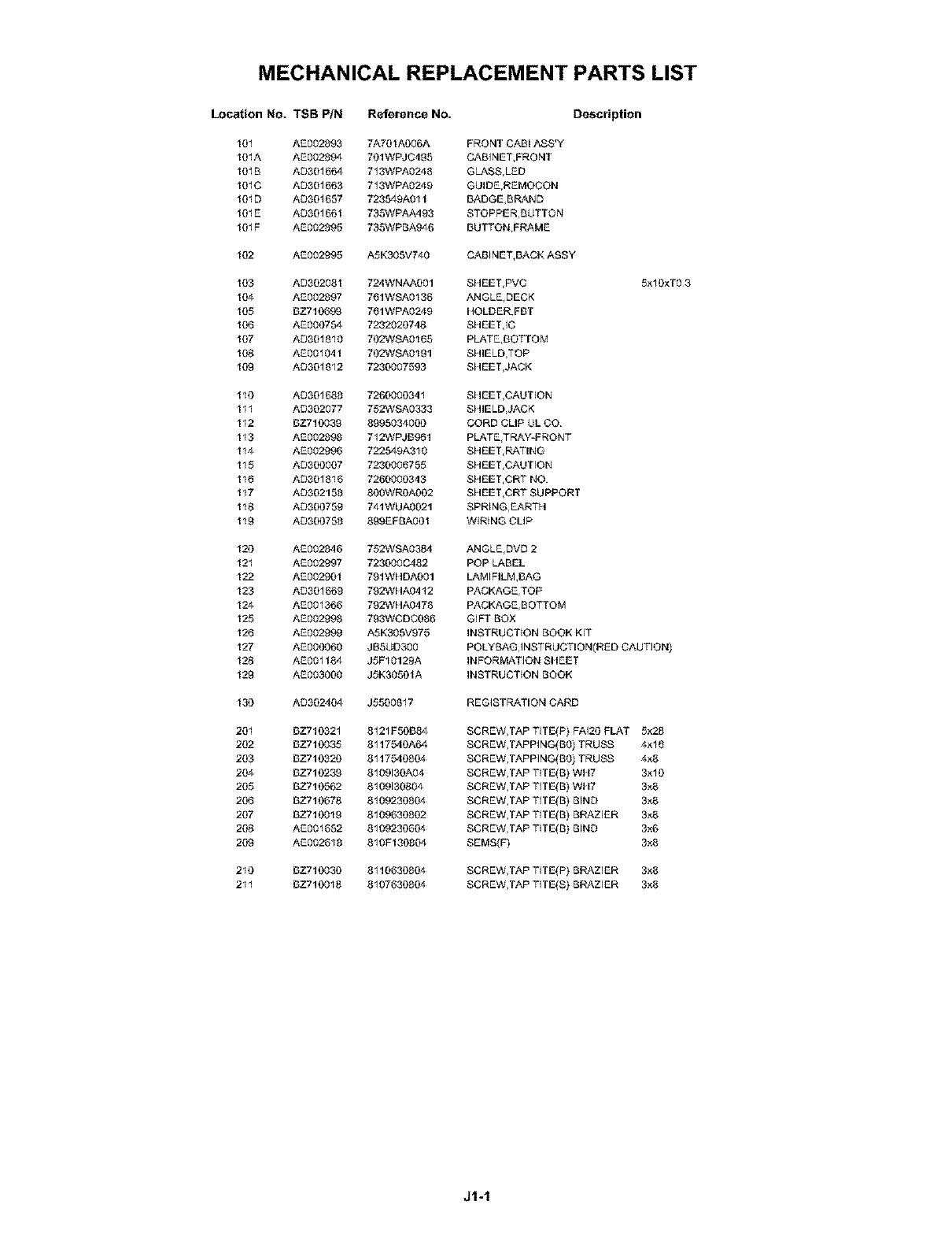
MECHANICAL REPLACEMENT PARTS LIST
Location No. TSB PIN Reference No. Description
t0t AE002893 7A70t A006A FRONT CABI ASS'Y
t0tA AE002894 701WPJC495 CABINET,FRONT
t0tB AD30t664 713WPA0248 GLASS,LED
t0tC AD30t663 713WPA0249 GUIDE,REMOCON
t0tD AD30t657 723549A01 t BADGE,BFLI:_ND
t0tE AD30t66t 738WPAA493 STOPPER,BUTTON
t0tF AE002895 738WPBA946 BUTTON,FRAME
t02 AE002995 ASK305V740 CABINET,BACK ASSY
t03 AD30208t 724WNAA001 SHEET,PVC
t04 AE002897 781WSA0136 ANGLE,DECK
105 BZ710699 781WPA0249 140LDER,FBT
t06 AE000754 7232020748 SHEETIIC
t07 AD30t810 702WSA0185 PLATE,BOTTOM
t08 AE00t04t 702WSA0191 SHIELD,TOP
t09 AD30t812 7230007593 SHEET,JACK
tll
t12
t13
t14
t15
t18
t17
t18
t19
t20
t21
t22
t23
t24
t25
t28
t27
t28
t29
t30
20t
2O2
203
204
2O5
206
2O7
200
2O9
2"_0
21t
AD301688 7280000341 SHEETICAUTION
AD302077 752WSA0333 SHIELDIJACK
BZ710039 8995034000 CORD CLIP UL CO.
AE002898 712WPJB001 PLATE,TRAY-FRONT
AE002996 722549A310 SHEET,RATING
AD300007 7230006755 SHEET,CAUTION
AD30t816 7280000343 SHEET,CRT NO.
AD302158 800WROA002 SHEET,CRT SUPPORT
AD300759 741WUA0021 SPRING,_\RTH
AD300758 899EF BA00t WIRING CLIP
AE002846 752WSA0384 ANGLEIDVD 2
AE002997 723000Ct82 POP LABEL
AE00290t 791WHDA001 L,_\MIFILM,EAG
AD30t669 792WHA0412 PACKAGE,TOP
AE00t366 792WHA0478 PACKAGE,BOTTOM
AE002998 793WCDC086 GIFT BOX
AE002999 ASK305V975 INSTRUCTION BOOK KIT
AE000060 JBSUD300 POLYBAG,INSTRUCTION(RED CAUTION)
AE00tt84 JSF10129A INFORMATION SI IEET
AE003000 JSK3000tA INSTRUCTION BOOK
AD302404 J5800817 REGISTRATION CARD
BZ71032t 8121F00B84 SCREW,TAP TITE(P) FAI20 FLAT 5x28
BZ710035 81175'|0A64 SCREW,TAPPING(B0) TRUSS 4×16
BZ710320 81175'|0804 SCREW,TAPPING(B0) TRUSS 4x8
BZ710239 8t09130A04 SCREW,TAP TITE(B) W117 3x10
BZ710562 8109130804 SCREW,TAP TITE(B} W117 3x8
BZ710678 8109230804 SCREW,TAP TITE(B} BIND 3x8
BZ710019 8109630802 SCREW,TAP TITE(B) BRAZIER 3x8
AE00t652 8109230604 SCREW,TAP TITE(B) BIND 3x6
AE002618 810Ft30804 SEMS(F} 3x8
BZ710030 8110630804 SCREW,TAP TITE(P) BRAZIER 3x8
BZ710018 8107630804 SCREW,TAP TITE(S} BRAZIER 3x8
5xlOxT03
J1-1
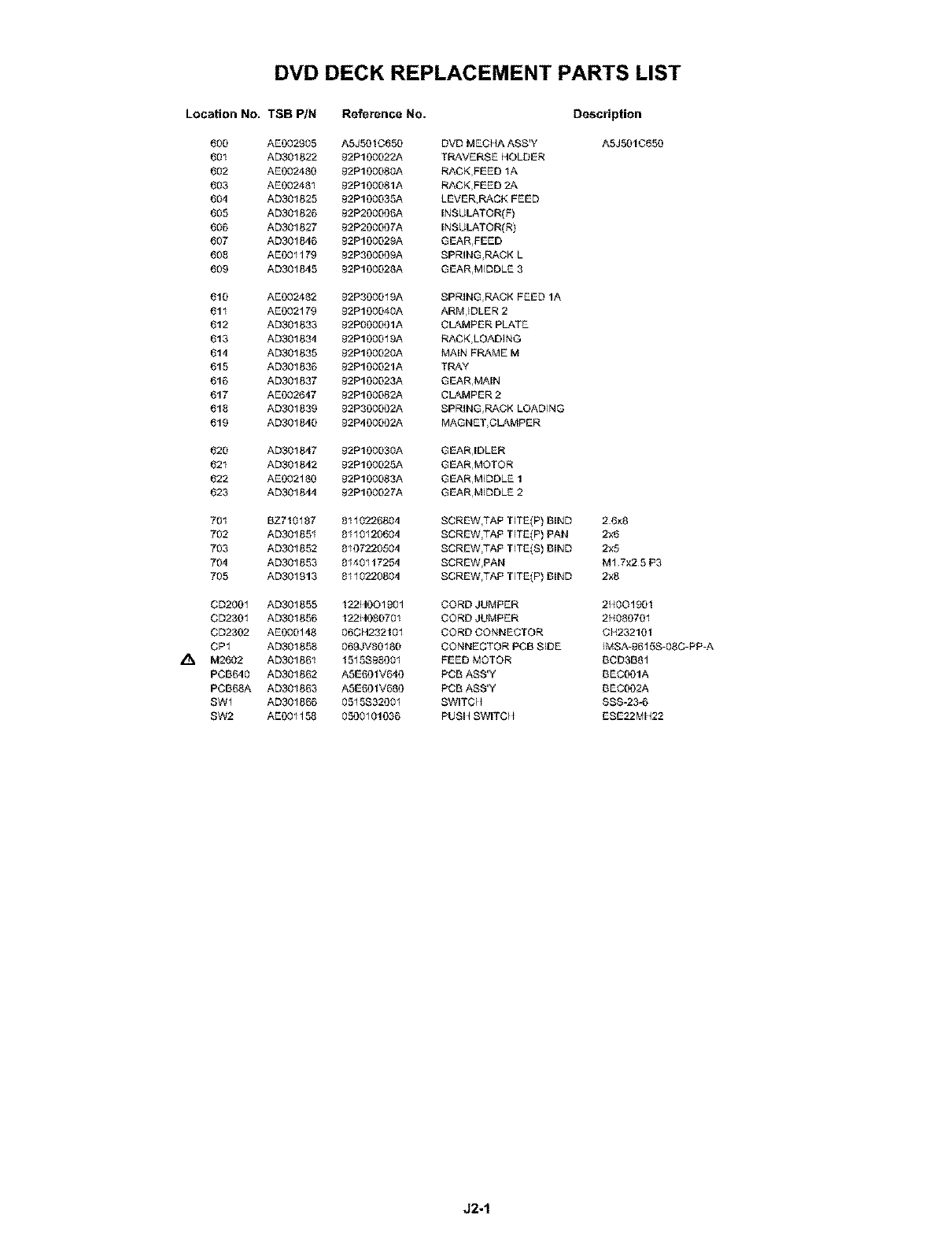
DVD DECK REPLACEMENT PARTS LIST
Location No. TSB PIN Reference No.
600 AE002905 A5JS01C650 DVD MECHA ASS'Y
601 AD301822 92P100022A TRAVERSE ItOLDER
602 AE002480 92P100080A RACKIFEED 1A
603 AE002481 92P100081A RACKIFEED 2A
604 AD301825 92P100035A LEVE R,FLI:',CKFEED
605 AD301826 92P200006A INSULATOR(F)
606 AD301827 92P200007A INSULATOR(R}
607 AD301846 92P100029A GEAR,FEED
60,5 AE001179 92P300009A SPRING,RACK L
609 AD301845 92P100028A GEARIMIDDLE 3
610 AE002482 92P300019A SPRING,RACK FEED 1A
611 AE002179 92P10004OA ARM,IDLER 2
612 AD301833 92PO00001A CLI_',MPER PLATE
613 AD301834 92P100019A RACK,LOADING
614 AD301835 92P10002OA MAIN FFLI_',MEM
615 AD301836 92P100021A TRAY
616 AD301837 92P100023A GEARIMAIN
617 AE002647 92P100082A CLI_',MPER 2
61,5 AD301839 92P300002A SPRING,RACK LOADING
619 AD301840 92P400002A MAGNETICLI_',MPER
620 AD301847 92P10003OA GEAR,IDLER
621 AD301842 92P100025A GEAR,MOTOR
622 AE002180 92P100083A GEAR,MIDDLE 1
623 AD301844 92P100027A GEARIMIDDLE 2
701 BZ7t0187 8110226804
702 AD301851 8110120604
703 AD301852 8107220504
704 AD301853 8140117254
705 AD301913 8110220804
DeecripUon
ASJ5010650
SCREW,TAP TITE(P) BIND 2 6×8
SCREW_TAP TITE(P) PAN 2×6
SCREW,TAP TITE(S) BIND 2x5
SCREW,PAN M1 7×25 P3
SCREW,TAP TITE(P) BIND 2×8
CD200t AD301855 12211001901 CORD JUMPER 2HOOt90t
0D230t AD301856 12211080701 CORD JUMPER 2H08070t
CD2302 AE000148 06CIt232t0t CORD CONNECTOR CH23210t
CPt AD301858 069JV80t80 CONNECTOR POE SIDE IMSA-9615S-08C-PP-A
,_ M2602 AD301861 1515898001 FEED MOTOR BCD3B81
PCB640 AD301862 ASE601V640 PCB ASS'Y BEC001A
PCB68A AD301883 A5E60tV680 PCB ASS*Y BEC002A
SWt AD301866 0515832001 SWITCH S88-234}
SW2 AE001 t58 0500101036 PUSH SWITCH ESE22MH22
J2-1
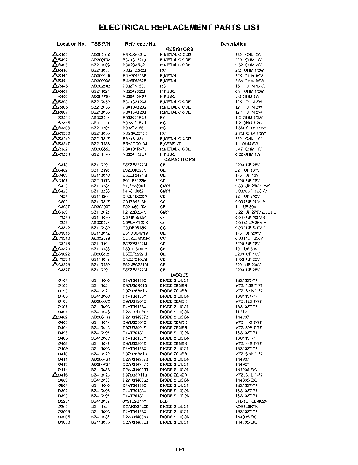
ELECTRICAL REPLACEMENT PARTS LIST
Location No.
,4_R401
_R4O2
,_,R400
,_R4t0
_R442
,_,R444
,_R445
_R447
R450
,_R803
_R805
,_,R807
R2_14
R2345
,1_,R3803
f_,R3806
_R3812
,1_,R3817
,._R3821
_R3828
C3t3
_0402
,_,0403
,_0407
C423
,_,0428
C431
C802
03007
,A0380t
03810
03811
03812
_03815
,_.03816
C3818
_03820
,1_,03822
,'_03823
_03826
C3827
D101
D102
D103
D105
D106
D107
D401
,_,D402
D403
D404
D405
D406
D408
D409
D4t0
D4tl
D4t3
D4t4
_D4t6
D603
D801
D802
D803
D220t
D260t
D3003
D3005
D3006
TSB PiN Reference No. Description
RESISTORS
AD301016 R3X28A331J R,METAL OXIDE
AD300783 R3Xt81221J R,METAL OXIDE
BZ210009 R3X28AR82J R,METAL OXIDE
BZ210053 R002T22R2J RC
AD300419 R4XST6223F R,METAL
AD300036 R4XST6562F R,METAL
AD302182 R002T4153J RC
BZ210021 R65582680J R,FUSE
AD30t76t R635815RCJ R,FUSE
BZ210050 R3XtSA123J R,METAL OXIDE
BZ210050 R3XtSA123J R,METAL OXIDE
BZ210050 R3XtSA123J R,METAL OXIDE
AE002014 R00202t R2J RC
AE002014 R00202t R2J RC
BZ210206 R002T2155J RO
BZ210080 ROG3K2275K RO
BZ210217 R3Xt81331J R,METAL OXIDE
BZ210t88 RSY2CD0t0J R,CEMENT
AD300659 R3Xt81R47J R,METAL OXIDE
BZ210t90 R63581R22J R,FUSE
CAPACITORS
BZt10t0t ES_;£F3222M CE
BZt10t95 E02LU8220M CE
BZt10016 ES_;£T2471M CE
BZ210t76 E02LF3222M CE
BZt10t36 P4J7F3394J CMPP
BZt10258 P4NSFJ862H CMPP
BZt 10204 EOELFD220M CE
BZt10247 COJBB0713K CC
AD302087 E02L05010M CE
BZt10025 P2122B224M CMP
BZt10080 COJOB0513K C0
AE000874 COPLRR7E3K CO
BZt10080 COJOB0513K CC
BZt10012 E510GO471M OE
AE002878 CD39EOMQ3M CC
BZt10t0t ES_;£F3222M CE
BZt10t88 ES011U5100M CE
AD300125 ES_F2222M CE
BZt10032 ES_;£F3102M CE
BZt10t30 E62NFC221M CE
BZt10t0t ES_;£F3222M CE
DIODES
BZ410006 DIVT001330 DIODE,SILICON
BZ410021 D97U05R61 B DIODE,ZENER
BZ410021 D97U05R61 B DIODE,ZENER
BZ410006 DIVT001330 DIODE,SILICON
AD300070 D97U01201B DIODE,ZENER
BZ410006 DIVT001330 DIODE,SILICON
BZ410043 D2WT011E10 DIODE,SILICON
AD30073t D2WXN49370 DIODE,SILICON
BZ410019 D97U03001 B DIODE,ZENER
BZ410019 D97U03001 B DIODE,ZENER
BZ410006 DIVT001330 DIODE,SILICON
BZ410006 DIVT001330 DIODE,SILICON
BZ410037 D97U03301 B DIODE,ZENER
BZ410006 DIVT001330 DIODE,SILICON
BZ410022 D97U06R81 B DIODE,ZENER
AD30073t D2WXN49370 DIODE,SILICON
AD30073t D2WXN49370 DIODE,SILICON
BZ410085 D2WXN40050 DIODE,SILICON
BZ410020 D97U05Rt tB DIODE,ZENER
BZ410085 D2WXN40050 DIODE,SILICON
BZ410006 DIVT001330 DIODE,SILICON
BZ410006 DIVT001330 DIODE,SILICON
BZ410006 DIVT001330 DIODEISILICON
BZ410087 0021E2Q140 LED
BZ410t21 DDARDS1200 DIODE,SILICON
BZ410006 DIVT001330 DIODE,SILICON
BZ410085 D2WXN40050 DIODE,SILICON
BZ410085 D2WXN40050 DIODEISILICON
330 OIIM 2W
220 OIIM lW
082 OIIM 2W
22 OItM t/2W
22K OHM t/6W
56K OI4M t/6W
15K QIIM 1i4W
68 OI4M t/2W
56 OHM lW
12K QIIM 2W
12K QIIM 2W
12K OIIM 2W
12 OHM t/2W
12 OHM 1/2W
15M OHM 1/2W
27M OHM 1/2W
330 QIIM lW
1 OHM 5W
047 OIIM lW
022 OI4M tW
2200 UF 25V
22 UF 100V
470 UF 16V
2200 UF 25V
039 UF 250V PMS
0 0086UF t25KV
22 UF 250V
000t UF 2KV B
1UF 50V
022 UF 275V ECQUL
000t UF 500V B
00015UF2KV R
000t UF 500V B
470 UF 200V
0 0047UF 250V
2200 UF 25V
10 UFSOV
2200 UF t6V
1000 UF 25V
220 UF 200V
2200 UF 25V
1SSt33T-77
MTZJS.CB T-77
MTZJS.CS T-77
1SSt33T-77
MTZJ12B T-77
1SSt33T-77
11Et-EIC
1N4937
MTZJ30B T-77
MTZJ30B T-77
1SSt33T-77
1SSt33T-77
MTZJ33B T-77
1SSt33T-77
MTZJC.SB T-77
1N4937
1N4937
1N4005-EIC
MTZJS.t B T-77
1N4005-EIO
1SSt33T-77
1SSt33T-77
tSSt33T-77
LTL-1CI IEE-002A
KDS120RTK
1SSt33T-77
1N4005-EIC
1N4005-EIC
J3-1
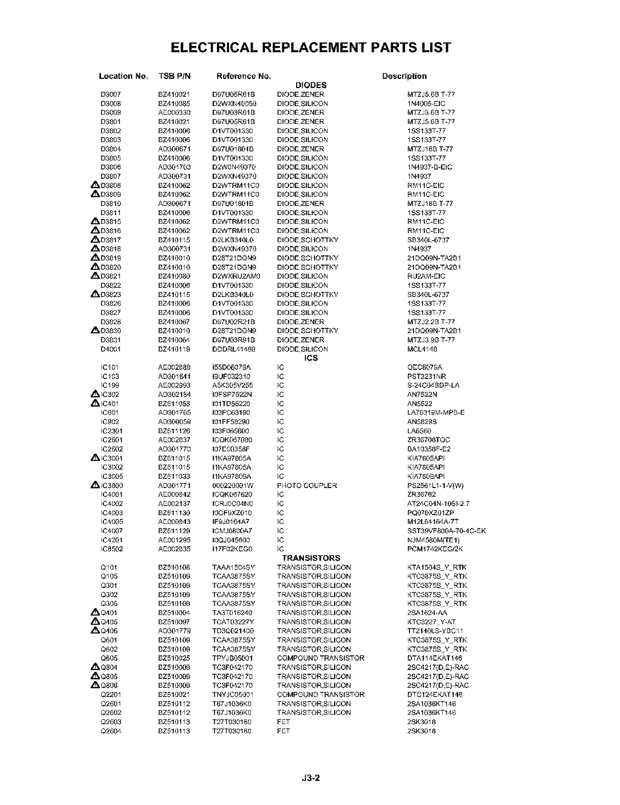
ELECTRICAL REPLACEMENT PARTS LIST
Location No.
D3007
D3008
D300g
D380t
D3802
D3803
D3804
D3805
D3806
D3807
_D3808
_,D380g
D3810
D381t
_,D3815
,'_,D3816
_D3817
_,D3818
,'_,D381g
_D3820
_,D3821
D3822
_D3823
D3826
D3827
D3828
_,D3830
D383t
D400t
10101
10103
10199
,_10302
_1C40_
10601
10902
IC230t
IC260t
IC2602
_C300t
IC3002
IC3005
_C3800
_C400t
_C4002
IC4003
_C4005
_C4007
IC420t
IC8502
Q101
Q105
Q301
Q302
Q305
,A0401
_0405
_,Q406
O601
Q602
0605
,_Q_o4
_o_o5
,_,Q806
Q220t
Q260t
Q2602
Q2603
Q2604
TSB P/N Reference No. Description
DZ410021 D97U05R61S
DZ410085 D2WXN40050
AE000330 D97U03R61B
DZ410021 D97U05R61B
DZ410006 DIVT001330
DZ410006 DIVT001330
AD30067t D97U01801B
DZ410006 DIVT001330
AD30t703 D2WON49370
AD30073t D2WXN49370
DZ410062 D2WTRM11C0
DZ410062 D2WTRM11C0
AD30067t D97U01801B
DZ410006 DIVT001330
DZ410062 D2WTRM11C0
DZ410062 D2WTRM11C0
DZ410t15 D2LKB340L0
AD30073t D2WXN49370
DZ410010 D28T21DQN9
DZ410010 D28T21DQN9
DZ410080 D2WXRU2&M0
DZ410006 DIVT001330
DZ410t15 D2LKB340L0
DZ410006 DIVT001330
DZ410006 DIVT001330
DZ410067 D97U02R21B
DZ410010 D28T21DQN9
DZ410064 D97U03RgtB
DZ410tlg DDDRL41480
AE002888 155D0607gA
AD30t64t 19UF0323t0
AE002993 ASK305V255
AD3021,54 10FSP7522N
DZ61t053 101TD55220
AD30t765 103FC631g0
AD300059 101FF582g0
DZ61tt26 103F065600
AE002837 IOQK067080
AD30t770 107E00358F
BZ61t015 IR<A97805A
BZ61t015 IR<A97805A
BZ61t033 ItKA9780gA
AD30t77t 000220001W
AE000842 ICQK067620
AE002t37 ICRJOC04N0
BZ61tt30 10GF9XZ0t0
AE000843 IFgJ0164A7
£Z61112g ICMJ0800A7
AE00t295 10QJ045800
AE002835 117F02KEG0
BZ510t08 TAAA1504SY
BZ510t09 TCAA3875SY
BZ510t09 TCAA3875SY
BZ510t09 TCAA3875SY
8Z510t09 TCAA3875SY
8Z510004 TA3T016240
8Z510097 TCAT03227Y
AD30t779 TD3Q021400
8Z510t09 TCAA3875SY
8Z510t09 TCAA3875SY
8Z510025 TPYJB05001
8Z510009 TC3F042170
8Z510009 TC3F042170
8Z510009 TC3F042170
8Z51002t TNYJC05001
8Z510t12 T67J1036K0
BZ510t12 T67J1036K0
BZ510t13 T27T030180
BZ510t13 T27T030180
DIODES
DIODE ZENER
DIODE SILICON
DIODE ZENER
DIODE ZENER
DIODE SILICON
DIODE SILICON
DIODE ZENER
DIODE SILICON
DIODE SILICON
DIODE SILICON
DIODE SILICON
DIODE SILICON
DIODE ZENER
DIODE SILICON
DIODE SILICON
DIODE SILICON
DIODE SCHOTTKY
DIODE SILICON
DIODE SCHO'TTKY
DIODE SCHO'Ti"KY
DIODE SILICON
DIODE SILICON
DIODE SCHOTTKY
DIODE SILICON
DIODE SILICON
DIODE ZENER
DIODE SCHOTTKY
DIODE ZENER
DIODE SILICON
ICS
IC
IC
IC
IC
IC
IC
IC
IC
IC
IC
IC
IC
IC
PHOTO COUPLER
IC
IC
IC
IC
IC
IC
IC
TRANSISTORS
TRANSISTOR,SILICON
TRANSISTOR,SILICON
TRANSISTOR,SILICON
TRANSISTOR,SILICON
TRANSISTOR,SILICON
TRANSISTOR,SILICON
TRANSISTOR,SILICON
TRANSISTOR,SILICON
TRANSISTOR,SILICON
TRANSISTOR,SILICON
COMPOUND TRANSISTOR
TRANSISTOR,SILICON
TRANSISTOR,SILICON
TRANSISTOR,SILICON
COMPOUND TRANSISTOR
TRANSISTOR,SILICON
TRANSISTOR,SILICON
FET
FET
MTZJS.6B T-77
1N4005-EIC
MTZJ3.6B T-77
MTZJS.6B T-77
1SSt33T-77
1SSt33T-77
MTZJ18B T-77
1SSt33T-77
1N4937-B-EIC
1N4937
RM11C-EIC
RM11C-EIC
MTZJ18B T-77
tSSt33T-77
RM11C-EIC
RM11C-EIC
SB340L-6737
1N4937
21DO09N-TE',2B1
21DQ09N-TE',2B1
RU2&M-EIC
1SSt33T-77
SB340L-6737
1SSt33T-77
1SSt33T-77
MTZJ2.2B T-77
21 DQ09N-TE',2B t
MTZJ3.gB T-77
MCL4148
OEC6079A
PST3231NR
S-24C04 BDP-LA
AN7522N
AN5522
LA76319M-MPB-E
AN5829S
LA6560
ZR36708TQC
BA10358F-E2
KIA7805API
KIA7805API
KIA7809API
PS256t LI-IW(W}
ZR36762
AT24 C04 N-10SI-2 7
PQ070XZ0tZP
M12L64164,,_,,-7T
SST39VF800A-70-4 C-EK
NJM4580M(TE1)
PCM1742KEGi2K
KTAtS04S Y RTK
KTC3875S Y RTK
KTC3875S Y RTK
KTC3875S Y RTK
KT03875S Y RTK
2SAt624-AA
KTC3227 Y-AT
TT2140LS-YBC11
KTC3875S Y RTK
KTC3875S Y RTK
DTAt 14 EKATt46
2S04217(D,E}-RAC
2SC4217(D,E}-RAC
2SC4217(D,E}-RAC
DTCt24 EKATt46
2SAt036KT146
2SAt036KT146
2SK30t8
2SK30t8
J3-2
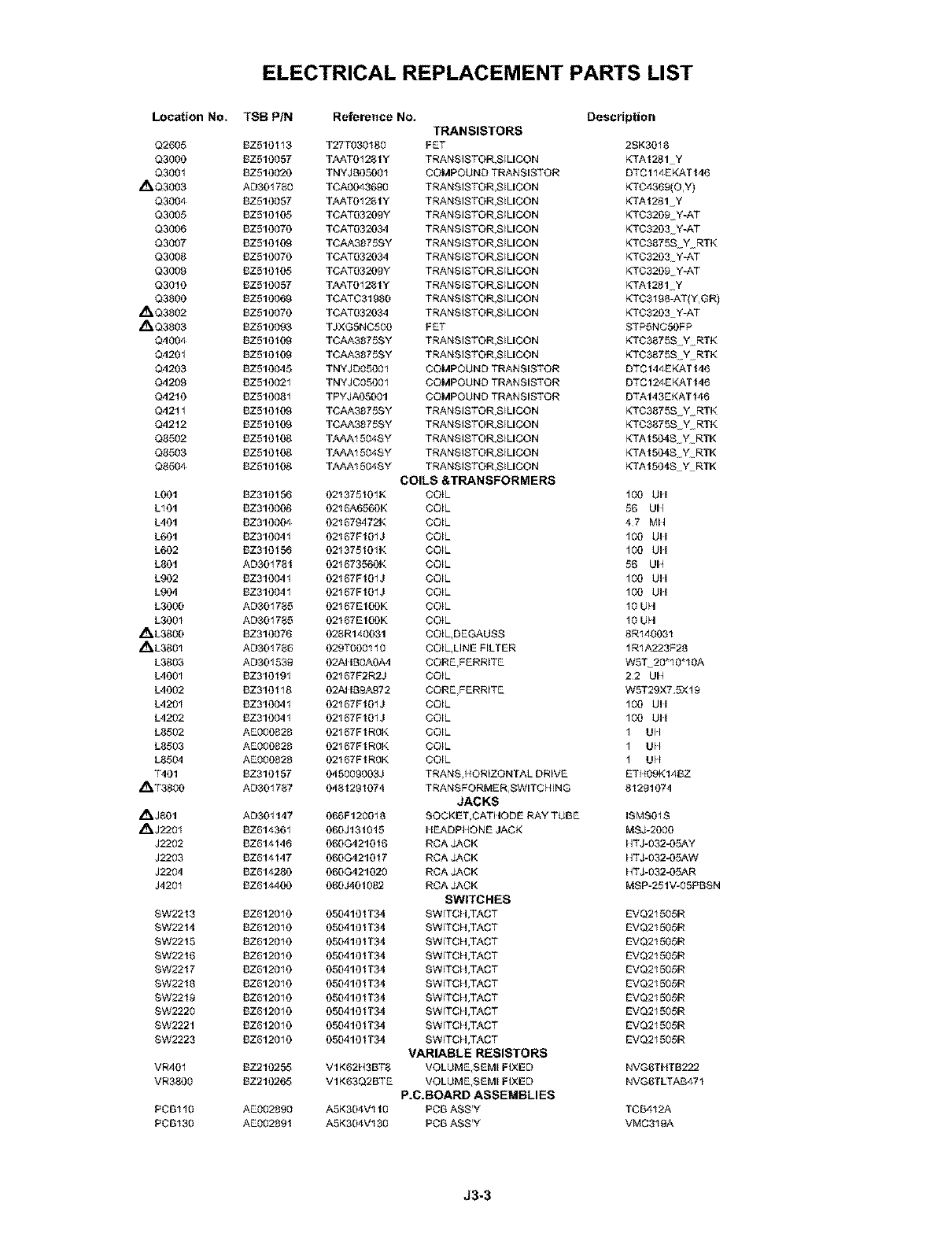
ELECTRICAL REPLACEMENT PARTS LIST
Location No.
O2605
O3000
O300t
/%,O3003
O3004
O3005
O3006
O3007
O3008
O3009
03010
03800
,/_,O3802
_O3803
O4004
O420t
O4203
O4209
O4210
O421t
O4212
O8502
O8503
O8504
L001
L101
L401
L601
L602
L801
L902
L904
L3000
L3001
,_,L3800
,/_,L3801
L3803
L4001
L4002
L4201
L4202
L8502
L8503
L8504
T401
_T38oo
,AjS01
_j220_
j2202
j2203
j2204
J4201
SW22t3
SW22t4
SW22t5
SW22t6
SW22t7
SW22t8
SW22t9
SW2220
SW2221
SW2223
VR40t
VR3800
PCB110
PCB130
TSB PIN Reference No. Description
TRANSISTORS
[3Z510t13 T27T030180 FET
BZ510057 TAAT01281Y TRANSISTOR,SILICON
BZ510020 TNYJB05001 COMPOUND TRANSISTOR
AD30t780 TCA0043690 TRANSISTOR,SILICON
BZ510057 TAAT01281Y TRANSISTOR,SILICON
BZ510t05 TCAT03209Y TRANSISTOR,SILICON
[3Z510070 TCAT032034 TRANSISTOR,SILICON
BZ510t09 TCAA3875SY TRANSISTOR,SILICON
[3Z510070 TCAT032034 TRANSISTOR,SILICON
BZ510t05 TCAT03209Y TRANSISTOR,SILICON
[3Z510057 TAAT01281Y TRANSISTOR,SILICON
[3Z510069 TCATC31980 TRANSISTOR,SILICON
[3Z510070 TCAT032034 TRANSISTOR,SILICON
8Z510093 TJXG5NCS00 FET
BZ510t09 TCAA3875SY TRANSISTOR,SILICON
[3Z510t09 TCAA3875SY TRANSISTOR,SILICON
[3Z510045 TNYJD05001 COMPOUND TRANSISTOR
[3Z510021 TNYJC05001 COMPOUND TRANSISTOR
[3Z51008t TPYJA05001 COMPOUND TRANSISTOR
BZ510t09 TCAA3875SY TRANSISTOR,SILICON
BZ510t09 TCAA3875SY TRANSISTOR,SILICON
BZ510t08 TAAA1504SY TRANSISTOR,SILICON
BZ510t08 TAAA1504SY TRANSISTOR,SILICON
BZ510t08 TAAA1504SY TRANSISTOR,SILICON
COILS &TRANSFORMERS
BZ310t56 021375t01K COIL
BZ310008 0216A6560K COIL
BZ310004 021679472K COIL
BZ31004t 02167Ft01J COIL
BZ310t56 021375t01K COIL
AD30t78t 021673560K COIL
BZ310041 02167Ft01J COIL
BZ31004t 02167Ft01J COIL
AD30t785 02167Et00K COIL
AD30t785 02167Et00K COIL
BZ310076 028R140031 COIL,DEGAUSS
AD30t786 029T0001 t0 COIL,LINE FILTER
AD30t539 02AI ISOAOA4 CORE,FERRITE
[3Z310t91 02167F2R2J COIL
BZ310t18 02AI IS9A972 CORE,FERRITE
BZ310041 02167Ft01J COIL
BZ310041 02167Ft01J COIL
AE000828 02167FtROK COIL
AE000828 02167FtROK COIL
AE000828 02167FtROK COIL
BZ310t57 045009003J TRANS,HORIZONTAL DRIVE
AD30t787 0481291074 TRANSFORMERISWITC} HNO
JACKS
AD30t147 066F1200t8 SOCKET,CATI lODE RAY TU[3E
BZ614361 060J13t0t5 I I['J\DPHONE JACK
BZ614t46 060G4210t6 RCA .JACK
BZ614t47 060G4210t7 RCA .JACK
BZ614280 060G421020 RCA .JACK
BZ614400 060J40t082 RCA .JACK
SWITCHES
[3Z612010 050410t T3'I SWITCH,TACT
BZ612010 050410t T3'I SWITCH,TACT
[3Z612010 050410t T3'I SWITCH,TACT
[3Z612010 050410t T3'I SWITCH,TACT
[3Z612010 050410t T3'I SWITCH,TACT
BZ612010 050410t T3'I SWITCH,TACT
[3Z612010 050410t T3'I SWITCH,TACT
[3Z612010 050410t T3'I SWITCH,TACT
[3Z612010 050410t T3'I SWITCH,TACT
[3Z612010 050410t T3'I SWITCI I,TACT
VARIABLE RESISTORS
[3Z210255 VIK6211313T8 VOLUME,SEMI FIXED
[3Z210265 VIK63Q213TE VOLUME,SEMI FIXED
P.C.BOARD ASSEMBLIES
AE002890 A5K304 V1t0 PC[3 ASS'V
AE00289t ASK304 V130 PC[3 ASS'Y
2SK3018
KTAt281 Y
DTCt 14EKATt46
KTC4369(O,Y}
KTAt281 Y
KTC3209 Y-AT
KTC3203 Y-AT
KTC3875S Y RTK
KTC3203 Y-AT
KTC3209 Y-AT
KTAt281 Y
KTC3198-AT(Y,GR)
KTC3203 Y-AT
STPSNCSOFP
KTC3875S Y RTK
KTC3875S Y RTK
DTCt44 EKATt46
DTCt24 EKATt46
DTAt43EKATt46
KTC3875S Y RTK
KTC3875S Y RTK
KTAtS04S Y RTK
KTAtS04S Y RTK
KTAtS04S Y RTK
t00 UII
56 UIt
47 MI4
100 Ull
t00 Ull
56 UI4
100 UII
100 UII
10 UH
10 UH
8R140031
1R1A223F28
WST 20"10"10A
22 UH
WST29X7.5X19
100 Ull
100 Ull
1 UH
1 UH
1 UH
[3TH09K1413Z
81291074
ISMS0tS
MS,J-2000
1tTJ-O32-05AY
ItT*J-032-05AW
I4T.J-032-05AR
MSP-251V-05PBSN
[3VQ21505R
[3VQ21505R
[3VQ21505R
[3VQ21505R
[3VQ21505R
[3VQ21505R
[3VQ21505R
[3VQ21505R
[3VQ21505R
[3VQ21505R
NVG6TI IT[3222
NVG6TLTAB471
TCB,112A
VMC319A
J3-3
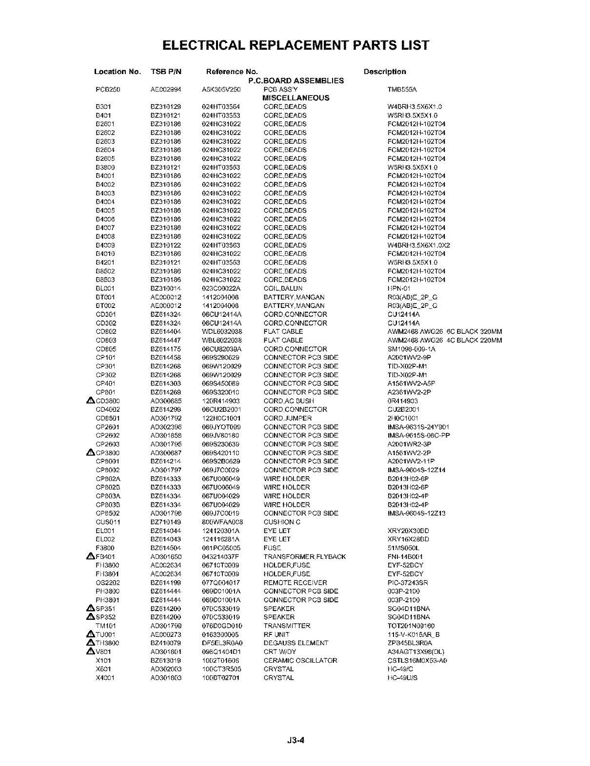
ELECTRICAL REPLACEMENT PARTS LIST
Location No.
PCE250
B301
B401
B260t
B2602
B2603
B2604
B2605
B3800
B400t
B4002
B4003
B4004
B4005
B4006
B4007
B4008
B4009
B4010
B420t
B8502
B8503
EL001
ST001
ST002
CD30t
CD302
CD802
CD803
CD805
CPt0t
0P30t
0P302
CP40t
CP80t
_OD3a00
CD4002
CD8501
CP2601
CP2602
CP2603
_CP3800
0P8001
CP8002
CPS02A
CPS02B
CPS03A
OPS03B
0P8502
OUS0t 1
EL001
EL002
F3800
_FB40t
FH3800
Fl/380t
OS2202
PH3800
Pl/3801
_SP351
_.SP352
TMt0t
_TU00t
/_,TH3800
AV801
X101
X601
X400t
TSB PIN Reference No.
P.C.BOARD ASSEMBLIES Description
AE002994 A5K305V250 PCE ASS'Y TMB555A
MISCELLANEOUS
BZ310t29 02411T0356_| CORE,BEADS W4BRIt3 5X6X1.0
BZ310t21 0241IT03553 CORE,BEADS WSRH3 5X5Xt 0
BZ310t86 02411031022 CORE,BEADS FCM2012H-102T04
BZ310t86 02411031022 CORE,BEADS FCM2012H-102T04
BZ310t86 02411031022 CORE,BEADS FCM2012H-102T04
BZ310t86 02411031022 CORE,BEADS FCM2012H-102T04
BZ310t86 02411031022 CORE,BEADS FCM2012H-102T04
BZ310t21 0241IT03553 CORE,BEADS W5RH3 5X5Xt 0
BZ310t86 02411031022 CORE,BEADS FCM2012H-102T04
BZ310t86 02411031022 CORE,BEADS FCM2012H-102T04
BZ310t86 02411031022 CORE,BEADS FCM2012H-102T04
BZ310t86 02411031022 CORE,BEADS FCM2012H-102T04
BZ310t86 02411031022 CORE,BEADS FCM2012H-102T04
BZ310t86 02411031022 CORE,BEADS FCM2012H-102T04
BZ310t86 02411031022 CORE,BEADS FCM2012H-102T04
BZ310t86 02411031022 CORE,BEADS FCM2012H-102T04
BZ310t22 0241IT03563 CORE,BEADS W4BRI43 5X6X%0X2
BZ310t86 02411031022 CORE,BEADS FCM201214-102T0.4
BZ310t21 0241IT03553 CORE,BEADS WSRH3 5X5Xt 0
BZ310t86 02411031022 CORE,BEADS FCM2012H-102T04
BZ310t86 02411031022 CORE,BEADS FCM2012H-102T04
BZ310014 023000022/-, COIL,BALUN HPN-01
AE000012 1412004008 BATTERYIMANGAN R03(AB}E 2P Q
AE000012 1412004008 BATTERY,MANGAN R03(AB}E 2P O
BZ614324 060U12414A CORD,CONNECTOR CU12414A
BZ614324 060U12414A CORD,CONNECTOR CU12414A
BZ614404 WDL6032038 FLAT CABLE AWM2468 AWQ26 60 BLACK 320MM
BZ614447 WBL6022038 FLAT CABLE AWM2468 AWQ26 40 BLACK 220MM
BZ614t75 060U82039A CORD,CONNECTOR SM1098-009_1A
BZ614458 069S290629 CONNECTOR PCS SIDE A2001WV2-P
BZ614268 069W120029 CONNECTOR PCS SIDE TID-X02P-M1
BZ614268 069W120029 CONNECTOR PCS SIDE TID-X02P-M1
BZ614303 069S450089 CONNECTOR PCS SIDE A1561WV2-ASP
BZ614269 069S3200t0 CONNECTOR PCB SIDE A2361WV2-2P
AD300885 120R414903 CORD,AC BUSI4 0R4 t4903
BZ614299 060U2B2001 CORD,CONNECTOR CU2E2001
AD30t792 12211001001 CORD,JUMPER 2H001001
AD302396 069JYOT099 CONNECTOR POS SIDE IMSA-963 tS-24Y901
AD30t 858 069JV80180 CONNECTOR POS SIDE IMSA-9615S4)80-PP
AD30t 795 069S230639 CONNECTOR PCS SIDE A2001WR,2-3P
AD300887 069S420110 CONNECTOR PCS SIDE A1561WV2-2P
BZ614214 069S2B0629 CONNECTOR PCS SIDE A2001WV2-11P
AD30t 797 069J700029 CONNECTOR PCB SIDE IMSA-9604 S-12Zt4
BZ614333 067U006049 WIRE I IOLDER B20131102-6P
BZ614333 067U006049 WIRE I IOLDER B20131402-6P
BZ614334 067U004029 WIRE I IOLDER B201314024P
BZ614334 067U004029 WIRE I IOLDER B201314024P
AD30t708 060J7000t9 CONNECTOR PCB SIDE IMSA-O604S-12Zt3
BZ710t49 800WFAA008 CUStHON C
BZ614044 124t2030tA EYE LET XRY20X30BD
BZ614043 124t16281A EYE LET XRY16X28ED
BZ614504 081 P005005 FUSE 51MS050L
AD30t650 043214037F TRANSFORMERIFLYBAOK FNI-t4B001
AE002634 067t0T0009 I IOLDER,FUSB EYF-52EOY
AE002634 067t0T0009 I IOLDER,FUSE EYF-52ECY
BZ614 t99 077Q0040t 7 REMOTE RECEIVER PIO-37243SR
BZ614444 069D01001A CONNECTOR PCS SIDE 003P-2t00
BZ614444 069D01001A CONNECTOR PCB SIDE 003P-2t00
BZ614200 07005330t9 SPEAKER SQ04Dt1BNA
BZ614200 07005330t9 SPEAKER SG04Dt1BNA
AD30t799 076DOGD0t0 TRANSMITTER TOT201N09160
AE000273 0163300005 RF UNIT 115W-K015AR B
BZ410079 DFSEL3ROA0 DEGAUSS ELEMENT ZPB45BL3ROA
AD30t80t 098Q1404D1 CRT WiDY A34AGT13XOS(DL)
BZ613019 1002T0t606 CERAMIC OSCILLATOR CSTLSt 6MOX53-A0
AD302003 100CT3RS05 CRYSTAL I1049iC
AD30t803 100ET02701 CRYSTAL 14049U/S
J3-4

RESISTOR
CAPACITORS
ELECTRICAL REPLACEMENT PARTS LIST
RC .............. CARBON RESISTOR
CC .............. CEFL_Z',MICCARAC4TOR
CE ................ ALUMI ELECTROLYTIC CAPACITOR
CP ............... POLYESTER CAPACITOR
CPP ............. POLYPROPYLENE CAPACITOR
CPL ............. PLASTIC CAPACITOR
CMP ................. METAL POLYESTER CAPACITOR
CMPL ............ METAL PLASTIC CAFACITOR
CMI=P ............ METAL POLYPROPYLENE CAPACITOR
J3-5

TOSHIBA CORPORATION
1-I, _t-II_AUIT_ I-CHO_IE, N1tl _TO-I_ U TOK'_ O 105-S001 JAPAtNI
