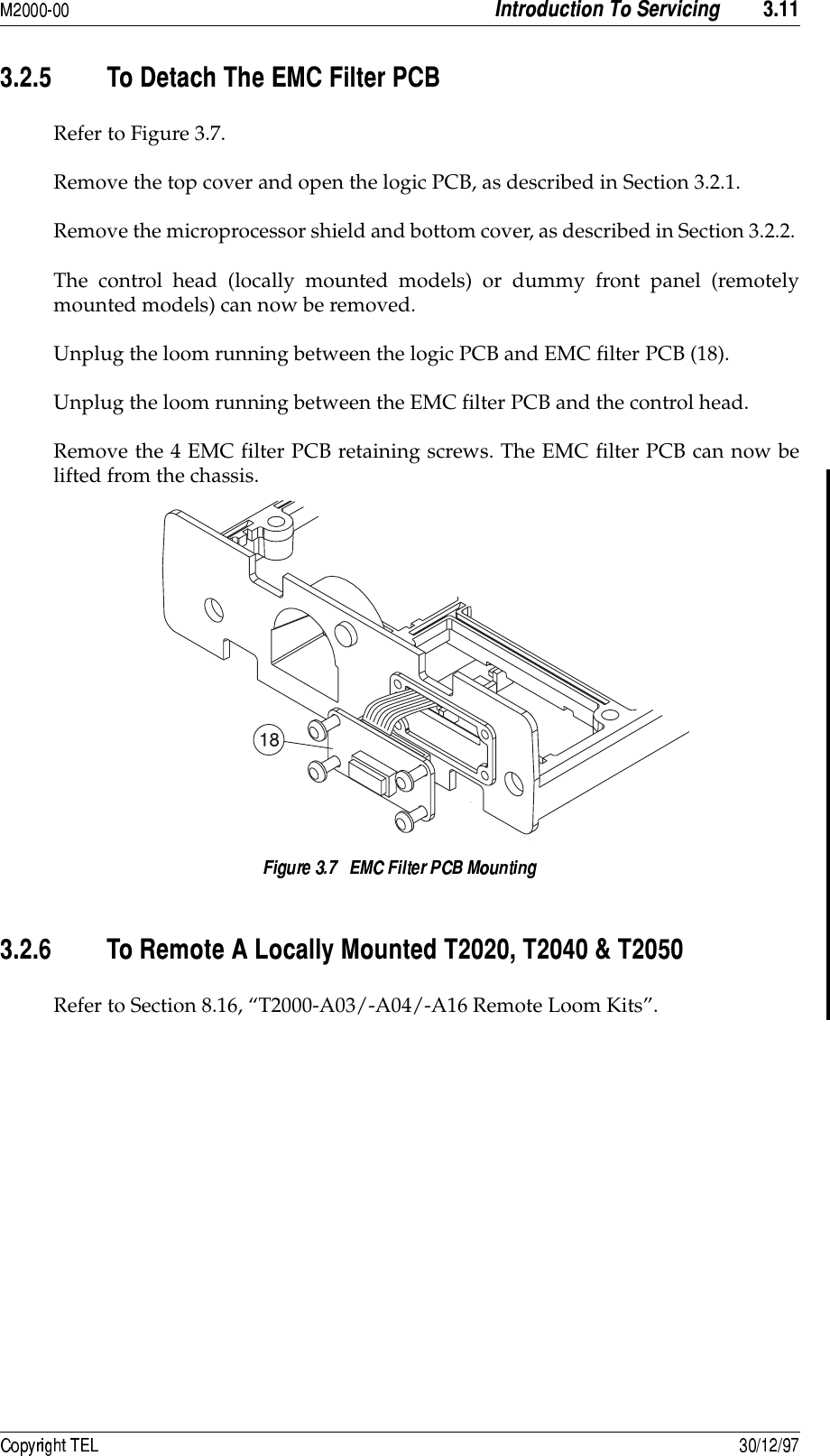
Tait 2000-6231 Mobile Transceiver User Manual 2k3 01
Tait Limited Mobile Transceiver 2k3 01
UserManual.wiki
>
Tait
>
2000-6231 User Manual
>
T2000 user manual part 1
Contents
1.
T2000 user manual part 1
2.
T2000 user manual part 2
3.
T2000 user manual part 3
4.
T2000 user manual part 4
5.
T2000 user manual part 5
6.
T2000 user manual part 6
7.
T2000 user manual part 7
8.
T2000 user manual part 8
9.
T2000 manual part 9
10.
T2000 manual part 10
T2000 user manual part 1
Navigation menu
Upload a User Manual
Namespaces
Wiki Guide
HTML
PDF
Info
Views
User Manual
Discussion / Help
Navigation

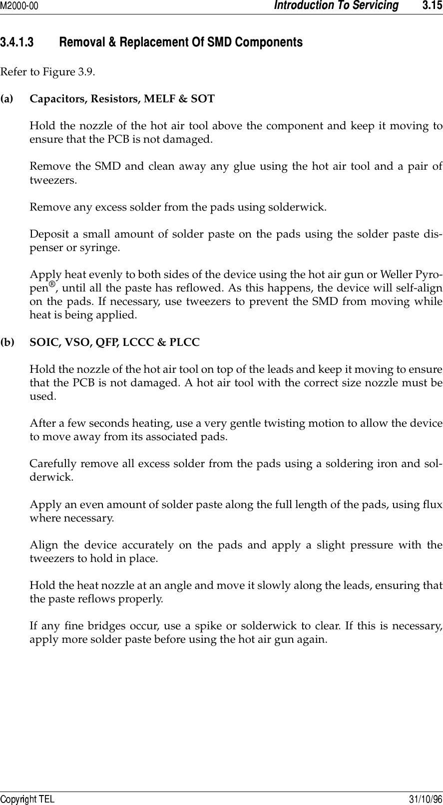
![ "8+"8" ##In this Section, deviation settings are given first for wide band, followed by settings formedium band in brackets ( ) and settings for narrow band in square brackets [ ]."8"8 )#9(#*&Connect a sinad meter across the speaker terminals.Connect an on-channel RF signal generator to the antenna input terminal.Disable any signalling control in T2010 or T2020 models by using the monitorfunction. The control head LED should now be active.Reduce the signal generator output level to -127dBm, modulated to ±3kHz(±2.4kHz) [±1.5kHz] deviation at 1kHz AF.Increase the RF output level until the squelch gate just opens.Check that the reading on the sinad meter is between 8 and 14dB.Reduce the signal generator output and check that the squelch gate closes within4dB of the original RF level."8"8 )#9(#Set the signal generator output level to -47dBm, modulated to ±5kHz (±4kHz)[±2.5kHz] deviation at 1kHz AF.Replace the sinad meter with an audio millivoltmeter across the speaker termi-nals.Adjust the volume control to the onset of clipping.Reduce the signal generator output level to -127dBm.The fall in output is the ‘squelch ratio’, and this should be at least 70dB.](https://usermanual.wiki/Tait/2000-6231.T2000-user-manual-part-1/User-Guide-352810-Page-75.png)
!["8- "8"8 )#9!*&,!Connect an audio millivoltmeter and an oscilloscope across the speaker terminals.Connect an on-channel RF signal generator to the antenna input socket, with theoutput set to -107dBm (1V) modulated to ±5kHz (±4kHz) [±2.5kHz] deviation at1kHz AF.Set the volume control to the onset of clipping.The receiver output should be 4.2Vrms across 4Ω at +13.8V supply.Check the distortion with the aid of a distortion analyser connected across thespeaker terminals.The distortion should not exceed 5%."8"8" )#9Connect a sinad meter across the speaker terminals.Connect the signal generator to the antenna input terminal.Set the signal generator accurately on the receive frequency.Set the modulation for ±3kHz (±2.4kHz) [±1.5kHz] deviation at 1kHz AF.Increase the signal generator output until a 20dB sinad is reached.Switch off the signal generator modulation.Couple a 10.7MHz reference oscillator loosely into the receiver IF stage, tune thesignal generator for a zero beat, then uncouple the reference oscillator.Set the signal generator deviation to ±3kHz (±2.4kHz) [±1.5kHz] at 1kHz AF. The modulating frequency must match the notch of the sinad meter.Set the signal generator output level to -127dBm.Disable the squelch control circuitry using the key on the T2010,T2015, T2020, T2050 or T2060, the key on the T203X, or “function21” on the T2040. The LED should then flash.Increase the signal generator output level until a sinad of 12dB is reached.The signal generator output should not be greater than -117dBm and is typically-119dBm.Fn](https://usermanual.wiki/Tait/2000-6231.T2000-user-manual-part-1/User-Guide-352810-Page-76.png)
![ "8."8"8+ )#9@AASet the signal generator output level to -107dBm modulated to ±5kHz (±4kHz)[±2.5kHz] deviation at 1kHz AF.Connect an audio millivoltmeter across the speaker terminals.Set the volume control for a reading of 0.8V (0dBm) on a convenient scale on themillivoltmeter.Switch off the signal generator modulation.Note the reading on the millivoltmeter.The fall in reading when the modulation is switched off should typically be 30dB(28dB) [25dB]."8"8- )#9%A A good quality RF signal generator with low residual FM must be used for thischeck (e.g. HP8640B or 8656).Set the signal generator to give an on-channel signal, modulated to ±5kHz(±4kHz) [±2.5kHz] with a 1kHz tone.Set the signal generator output level to -47dBm.Connect an AC millivoltmeter across the speaker terminals.Adjust the volume control for a reading of 0.8V (0dBm) on a convenient scale.Turn off the signal generator modulation.Note the reading on the millivoltmeter.The fall in reading when the modulation is switched off should be at least 50dB(48dB) [45dB]."8"8. $Set the signal generator to give an unmodulated signal at an output level of-120dBm.Increase the input level in 10dB steps over the 50dB dynamic range and monitorthe RSSI output on pin 15 of S14 (logic PCB).Ensure the output varies approximately 540mV/10dB over the dynamic range.](https://usermanual.wiki/Tait/2000-6231.T2000-user-manual-part-1/User-Guide-352810-Page-77.png)
!["8/ "8"8/ )#9*&*A69Connect an ignition noise simulator and an RF signal generator to the receiverantenna input.Set the signal generator modulation for ±3kHz (±2.4kHz) [±1.5kHz] deviation at1kHz AF.Set the signal generator output level to give a 20dB sinad.Listen to the receiver output and check the operation of the noise blanker by tem-porarily short circuiting R135 on the RF PCB to ground, thus disabling the noiseblanker.The noise blanker should give a marked reduction in noise over a wide range ofnoise input amplitudes.](https://usermanual.wiki/Tait/2000-6231.T2000-user-manual-part-1/User-Guide-352810-Page-78.png)
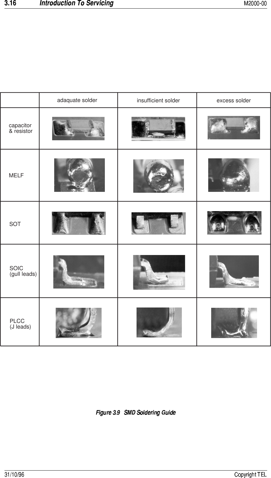
![ "80"8+ #In this Section, deviation settings are given first for wide band, followed by settings formedium band in brackets ( ) and settings for narrow band in square brackets [ ]."8+8 !#"8+88 )#9,)#*&Connect an oscilloscope to monitor the waveform at TSP901 (TCXO PCB).Plug the microphone test lead into the control head microphone input socket.Apply a 1kHz sine wave.Slowly increase the sine wave output level until the waveform begins to distort(squaring), indicating that limiting has commenced.Any further increase in sine wave output level should not increase the amplitudeof the waveform."8+88 )#9!!,)*&Connect an oscilloscope to monitor the waveform at TP606 (logic PCB).Apply a 1kHz sine wave.Connect an EVM to the junction of R667 and C639.Increase the sine wave output level to 10dB above the limiting level, as describedin Section 4.5.1.1.Note the amplitude on the oscilloscope, then increase the output level by another10dB.Check that the amplitude of the waveform does not increase or distort signifi-cantly.The EVM should show a positive DC reading.](https://usermanual.wiki/Tait/2000-6231.T2000-user-manual-part-1/User-Guide-352810-Page-79.png)
!["81 "8+88 )#92*!#Connect the T2000 antenna output via a 30dB attenuator to a modulation meter.Plug the microphone test lead into the control head microphone input socket.Apply a 1kHz sine wave and adjust the output level to give a 3kHz (2.4kHz)[1.5kHz] deviation reading on the modulation meter.Connect a millivoltmeter across the input of the microphone test box and checkfor a reading of approximately 1mVrms on the millivoltmeter. The audio processor gain must be checked at a level below that at which theaudio ALC or limiting are influencing the measurements."8+8 )##"8+88 )#9!,&Connect the T2000 antenna output via a 30dB attenuator to a modulation meter.Plug the microphone test lead into the control head microphone input socket.Apply a 1kHz sine wave and increase the output level to 20dB above the limitinglevel, as described in Section 4.5.1.1.Vary the frequency of the sine wave generator between 0.3 and 5kHz.Note the reading on the modulation meter.The deviation should not exceed ±5kHz (±4kHz) [±2.5kHz].Between 450Hz and 3kHz (3kHz) [2.55kHz] the deviation should be within 4dB ofmaximum.Above 3kHz the deviation should decrease by more than 25dB/octave."8+88 )#967,&Decrease the sine wave generator output level to 10dB below the limiting level, asdescribed in Section 4.5.1.1.Sweep the sine wave from 0.3 to 10kHz.Note the reading on the modulation meter.From 300Hz to 3kHz (3kHz) [2.55kHz] the deviation should increase at the rate of6dB/octave (+1, -3dB) relative to 1kHz.Above 3kHz the deviation should decrease by more than 25dB/octave.](https://usermanual.wiki/Tait/2000-6231.T2000-user-manual-part-1/User-Guide-352810-Page-80.png)
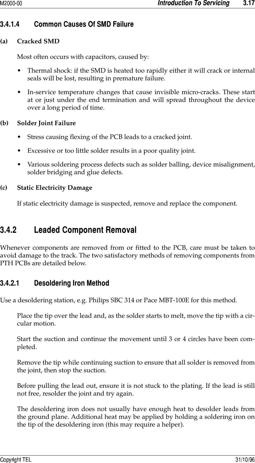
![+8- Program mode2010: all channel LEDs on2015: display shows “00”Display shows “-PROG-” Top row LEDs onTop row + C1 LEDs all on (if fitted)T2033/35: display shows “-UU”Display shows“-PROG-”Top row LEDs onCloning modeAUX LED flashing. AUX/SCAN LEDs flash if clone failed. Target radio in pro-gramming mode.Display shows “CLONING” Top row LEDs on. Tar-get radio in pro-gramming mode.Manual Test Mode(MTM)All LEDs on for a short time then indicate radio sta-tus.C1 to C4 show last channel (if fitted).T2035: display shows “- - -” brieflyDisplay shows “chan xxxx” (xxxx = last channel number). LEDs indicate radio sta-tusKey pressed at power-up(control head test)[AUX] = clone[CALL] = program Any key on the control head & any mode. All LEDs & all LCD segments are set flashing indefi-nitelyC1 key (if fitted) in MTM- a front panel key/LED test is initi-ated - all LEDs on initiallyAny key on the control head & any mode. All LEDs & all LCD segments are set flashing indefinitelyComputer Control-led Test Mode(CCTM)Front panel shows normal radio state (not a separate mode)Display shows “-AUTOTEST-” Top row LEDs onTop row + C2 LEDs (if fitted) all on.T2035: display shows "- - -" contin-uouslyDisplay shows “AUTOTEST” Top row of LEDs onCCI modeNormal display“CCI BUSY” & top row LEDs on when processing a com-mand or in ‘lockout all’ modeNormal display “CCI BUSY” & top row LEDs on when processing a com-mand or in ‘lockout all’ mode.Normal radiomodeNo special power-up sequence - nor-mal radio state immediatly dis-playedProgrammable power-up message displayed for a short time then nor-mal radio display (default mode)T2030: own number as CD on 3 rows of LEDs, then last number on C1 to C4 & DESP LEDs. Others as labelled.T2035: Own number briefly on display, then last number called.Own number dis-played for a short time after power-up then program-mable power-up message followed by normal radio displayPTT on power-up in MTM or normal modeSoftware version # indicated for a short time as “h.nn”. “h” is shown with the Busy and TX LEDs as a hex number. “n’s” are indicated by the two lower rows of LEDs (2010), or by the channel display (2015).Display shows “xxxx nn.mm” for a short time, nn = major, mm = minor version number T2030: 3 rows of LEDs display the software version # for a short time as h.nn (h is a hex number) then as per selected mode.T2035: software version numberon display.Display shows “xxxx nn.mm” for a short time, nn = major mm = minor version number, then as per selected modeMode/State T2010/T2015 T2020 T2030/T2035 T2040](https://usermanual.wiki/Tait/2000-6231.T2000-user-manual-part-1/User-Guide-352810-Page-98.png)
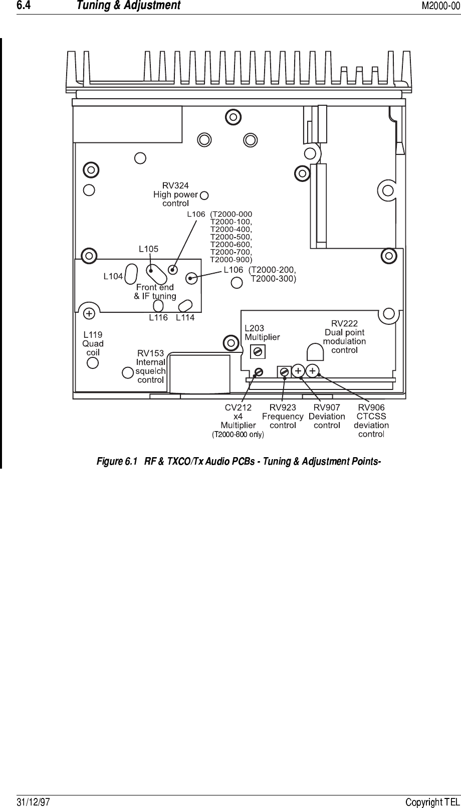
![ ! -8+-8 9The ‘test’ facility enables T2000 trunked radios to emulate a multichannel radio, usingthe frequencies reserved for trunking. For a description of how to put the radio in test mode, refer to Section 5.8 “TrunkedRadios: Test Mode”. Once the radio is in test mode, tuning and adjustment can be car-ried out as described in Section 6.4 and Section 6.5.) When in test mode, connect the antenna socket to a dummy load to pre-vent interference with trunking systems. Avoid testing on channels in uselocally.-8" !5In this Section, deviation settings are given first for wide band, followed by settings formedium band in brackets ( ) and settings for narrow band in square brackets [ ].-8"8 7*&Set up the test equipment as shown in Section 4, and close the PTT switch.Turn RV324 fully clockwise and check that the output power is greater than 30Wfor all channels.Select a channel programmed for high power and adjust RV324 for 25W.Check that the transmit current is approximately the values stated below:Select a channel programmed for low power and adjust RV507 for the requiredoutput power.Model CurrentT2000-100 6AT2000-200 6AT2000-300 6AT2000-400 6AT2000-500 6.5AT2000-600 7AT2000-700/900 6.5AT2000-800 6A](https://usermanual.wiki/Tait/2000-6231.T2000-user-manual-part-1/User-Guide-352810-Page-119.png)
![ ! -8.-8"8" ))!5The following instructions apply only to those radios with CTCSS activated andmust be carried out before any further modulation adjustment can proceed.Refer to the T2000 Programming Manual for the CTCSS channel programminginstructions. The frequency range of the CTCSS tone is 67 to 250.3Hz.Switch to any channel with CTCSS activated.Close the PTT switch.Adjust RV906, on the TCXO PCB, to set the CTCSS tone peak deviation for±660Hz ±100Hz (±530Hz ±80Hz) [±330Hz ±50Hz] on the modulation meter.-8"8+ ,)!5Close the PTT switch and set up a continuous call. This can be an LTR RepeaterTalkaround call, a Repeater Interconnect Call (RIC) or an on-channel call.Adjust RV906 on the TCXO PCB to set the LTR code deviation to ±1kHz (±900Hz)[±600Hz].A The deviation meter must have a good low frequency response to avoid incor-rect readings.-8"8- !5Complete the dual point modulation and CTCSS modulation adjustments (Sec-tion 6.4.3 and Section 6.4.4) before commencing the modulation adjustment.Apply a 3kHz sine wave at a level of -40dBm to the microphone input.Select a channel with CTCSS activated and close the PTT switch. If CTCSS is disa-bled, select any channel.Adjust RV907 for a +5kHz (+4kHz) [+2.5kHz] deviation reading on the modula-tion meter.Maintain the same sine wave output level and sweep the audio frequency from300Hz to 3.3kHz.Find the frequency of maximum ‘+’ deviation and readjust RV907 for +5kHz(+4kHz) [+2.5kHz] deviation.Reset the modulation meter to read ‘-’ deviation.Slowly sweep the audio frequency from 300Hz to 3kHz. If the ‘-’ deviation peak isfound to exceed -5kHz (-4kHz) [-2.5kHz], readjust RV907 for a peak deviation of-5kHz (-4kHz) [-2.5kHz] at that frequency.The peak deviation should not exceed ±5kHz (±4kHz) [±2.5kHz] on any channel.](https://usermanual.wiki/Tait/2000-6231.T2000-user-manual-part-1/User-Guide-352810-Page-121.png)
![-8/ !-8"8. #This is normally preset at 60% of voice deviation. If adjustment is needed, fit#RV508 (refer to Section 7 for a component description) to the logic PCB, and pro-ceed as follows.Adjust #RV508 for ±3kHz (±2.4kHz) [±1.5kHz] deviation reading on the modula-tion meter.Check to ensure that no limiting occurs in IC901.-8"8/ 33E!5>9*?-8"8/8 1 ;Enter test mode (refer to Section 5.8, “Trunked Radios: Test Mode”).Press the front panel # key .Adjust #RV599 for ±3kHz ±200Hz (±2.4kHz ±160Hz) [±1.5kHz ±100Hz] deviationreading on the modulation meter.-8"8/8 1"1Enter test mode (refer to Section 5.8, “Trunked Radios: Test Mode”).Select test function 10 using the control head.Adjust #RV599 for ±3kHz ±200Hz (±2.4kHz ±160Hz) [±1.5kHz ±100Hz] deviationreading on the modulation meter.2](https://usermanual.wiki/Tait/2000-6231.T2000-user-manual-part-1/User-Guide-352810-Page-122.png)
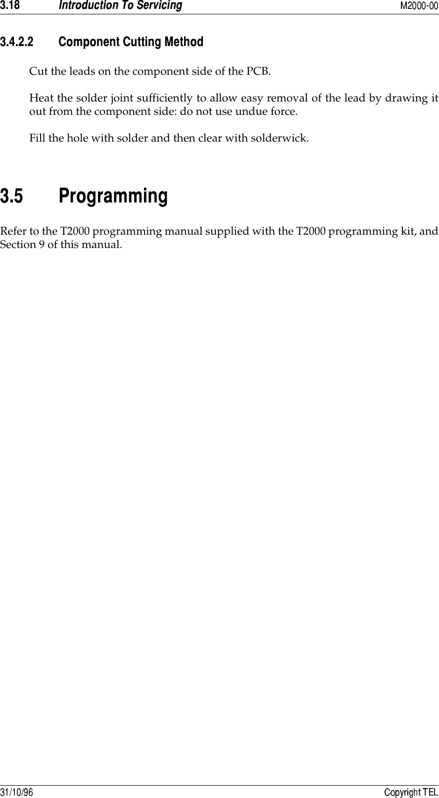
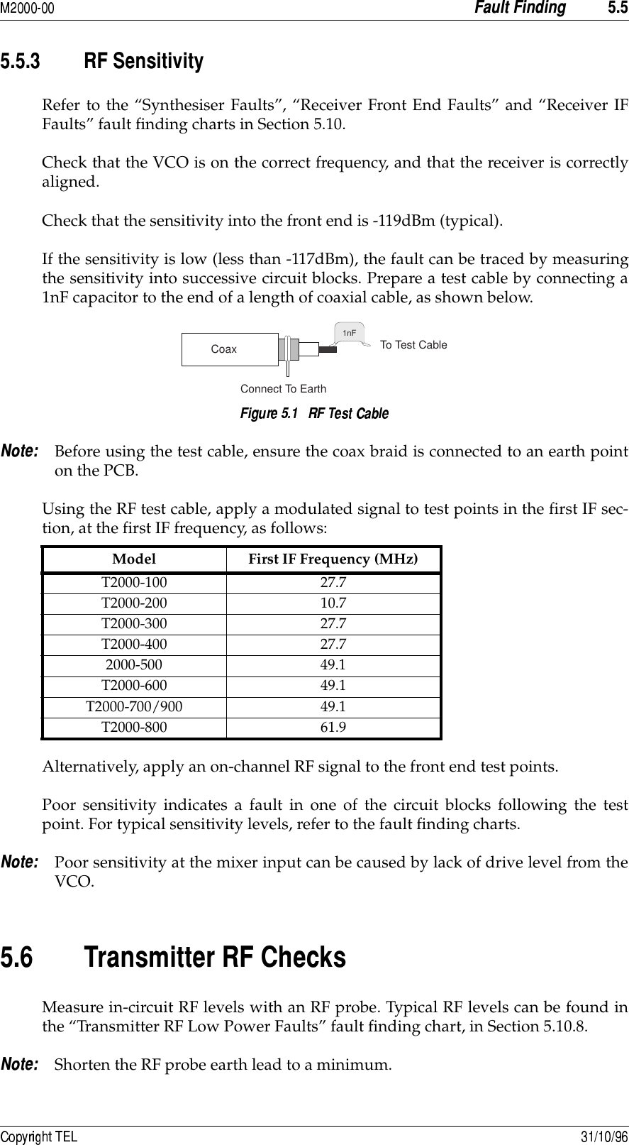
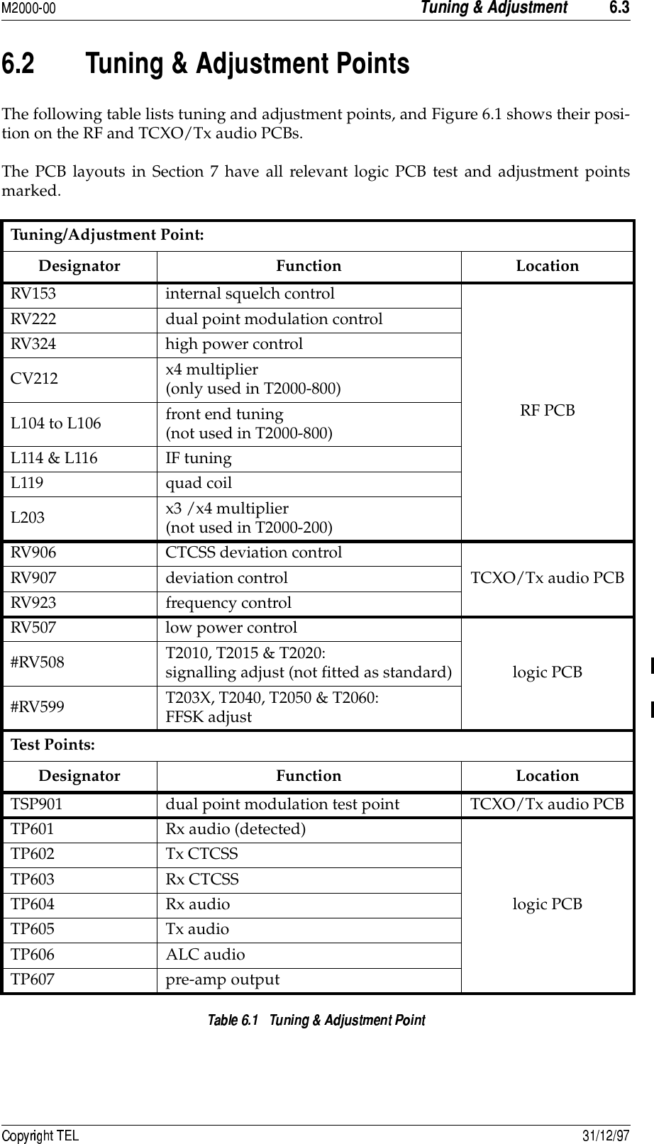
![ ! -80-8+ #!5In this Section, deviation settings are given first for wide band, followed by settings formedium band in brackets ( ) and settings for narrow band in square brackets [ ].-8+8 3!Set up the test equipment as shown in Section 4, and select the highest possiblefrequency in the operating band.Set the signal generator to the required receive frequency with modulation set for±3kHz (±2.4kHz) [±1.5kHz] deviation at 1kHz AF and an output level of-100dBm.Using the receiver tuning amplifier circuit shown in Figure 6.2, adjust RV1 untilthe voltage of point A equals 3.0V DC, measured on a 1MΩ digital multimeter.Connect the receiver tuning amplifier to the RSSI output on pin 15 of S14 (logicPCB) and monitor the output on an oscilloscope (1V/division, DC coupled).If the output on the oscilloscope is 0V DC, increase the RF input level above-100dBm until the output level just starts to rise.Adjust L104, L106, L105, L114, L116 and L203, in this order, to give maximumamplitude.A L203 is not used in the T2000-200.While tuning the coils, adjust the signal generator output so that the level on theoscilloscope does not exceed 6V DC.Monitor the audio output at the speaker terminals and adjust L119 for maximumamplitude.Set the squelch control (RV153) to minimum and connect a sinad meter across thespeaker terminals.Decrease the signal generator output until a 12dB sinad is reached.The signal generator output should not be greater than -117dBm.Switch to the lowest possible frequency in the operating band, and check that thereceiver sensitivity is better than -117dBm.C21µFR310kRV1100k(26 turn)IC1LM358123+-R112kinputfromRSSIR2390k+9V DCoutput tooscilloscope1V/div.(DC coupled)C11µF++A = 3V DC](https://usermanual.wiki/Tait/2000-6231.T2000-user-manual-part-1/User-Guide-352810-Page-123.png)
![-81 !-8+8 $)If required, the mute setting can be adjusted internally as follows.Align the receiver, as described in Section 6.5.1.Adjust RV153 fully clockwise.Set the signal generator to the required receive frequency.Set the modulation for ±3kHz (±2.4kHz) [±1.5kHz] deviation at 1kHz AF.Adjust the signal generator output for 11dB sinad.Adjust RV153 so that the radio mutes then turn RV153 until the mute gate justopens.-8+8 $The T2000 RSSI is non-adjustable and should operate over an approximate 50dBrange.Monitor the RSSI output on pin 15 of S14 on the logic PCB.Set the signal generator to the required receive frequency with modulation set for±3kHz (±2.4kHz) [±1.5kHz] deviation at 1kHz AF and an output level of -70dBm.Decrease the signal generator output in 10dB steps to -120dBm, noting the RSSIoutput at each step.The RSSI should have a typical slope of approximately 540mV/10dB, from-120dBm to -70dBm RF input.-8+8 8 F,D,%&>9*?These levels are factory set at the time of manufacture and will require reprogram-ming only if the receiver has been realigned or has had parts replaced, or if thelogic PCB has been replaced.Set the signal generator to give an unmodulated RF signal in the centre of thetrunking band.Enter test mode.A The T203X will need to use CCTM, as described in Section 5.8.3.Set the signal generator to -108dBm and program ‘L1’ (function 61), as describedin Section 5.8.5.2.Set the signal generator to -100dBm and program ‘L2’ (function 62), as describedin Section 5.8.5.2.](https://usermanual.wiki/Tait/2000-6231.T2000-user-manual-part-1/User-Guide-352810-Page-124.png)