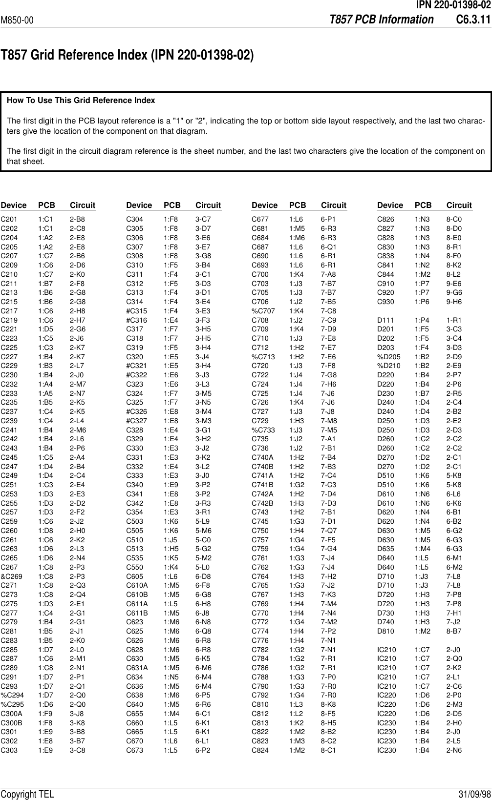
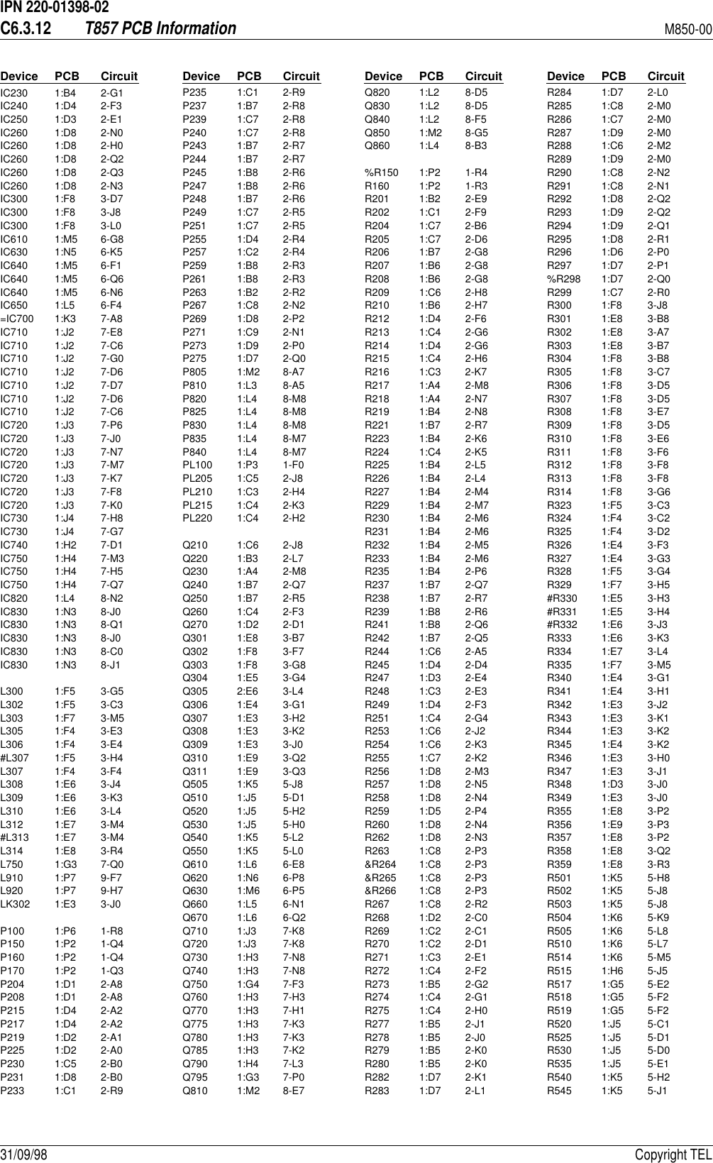
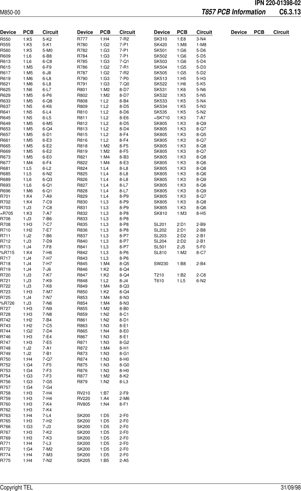
Tait TEL0020 Base Station Transmitter User Manual 8c500 a4 bk
Tait Limited Base Station Transmitter 8c500 a4 bk
UserManual.wiki
>
Tait
>
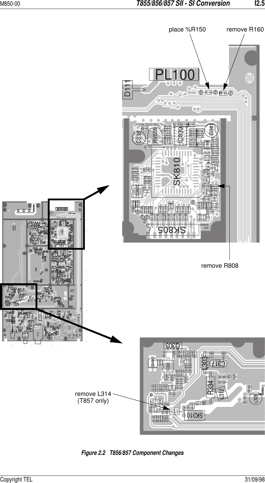
TEL0020 User Manual
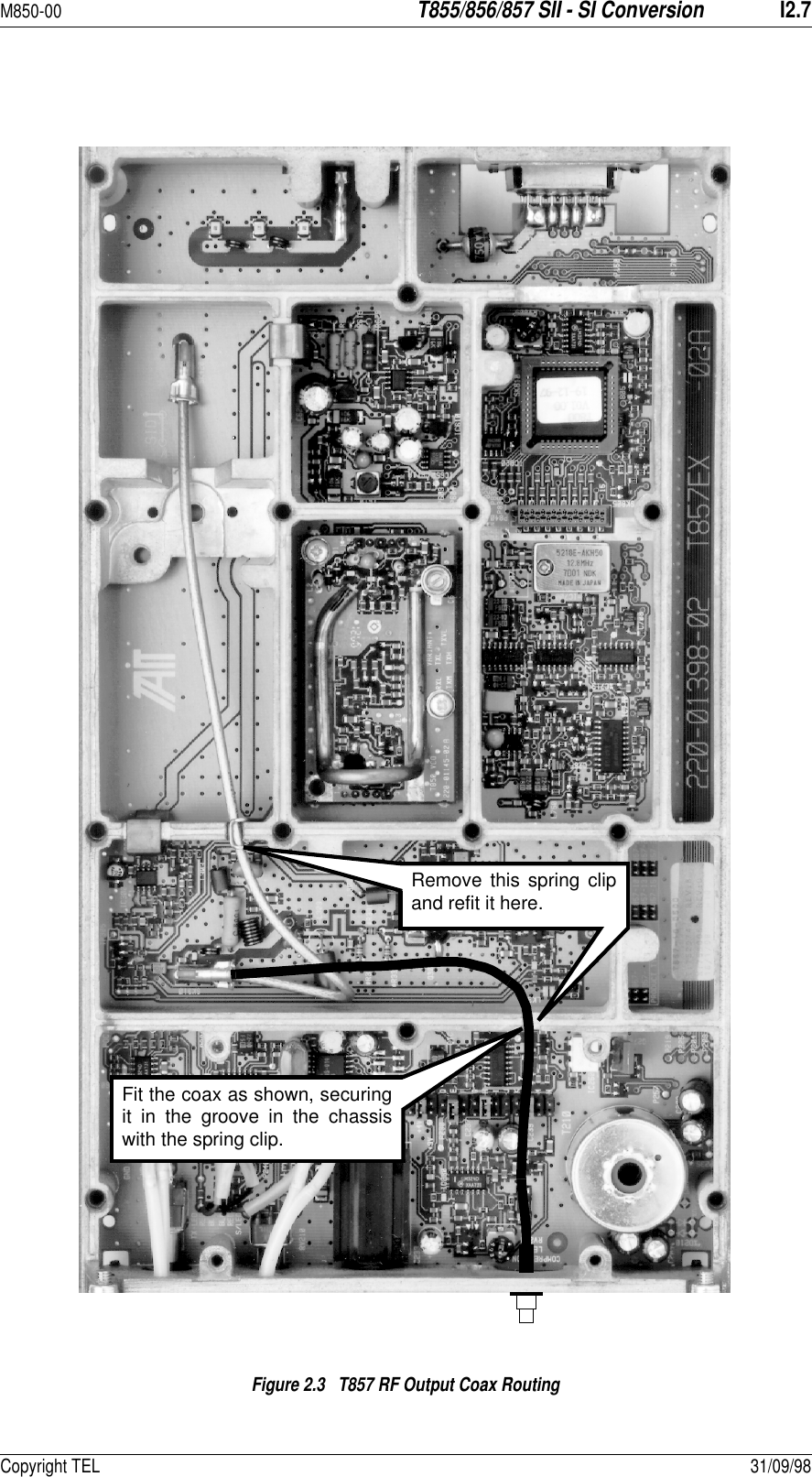
Descriptions Diagrams Info
Navigation menu
Upload a User Manual
Namespaces
Wiki Guide
HTML
PDF
Info
Views
User Manual
Discussion / Help
Navigation


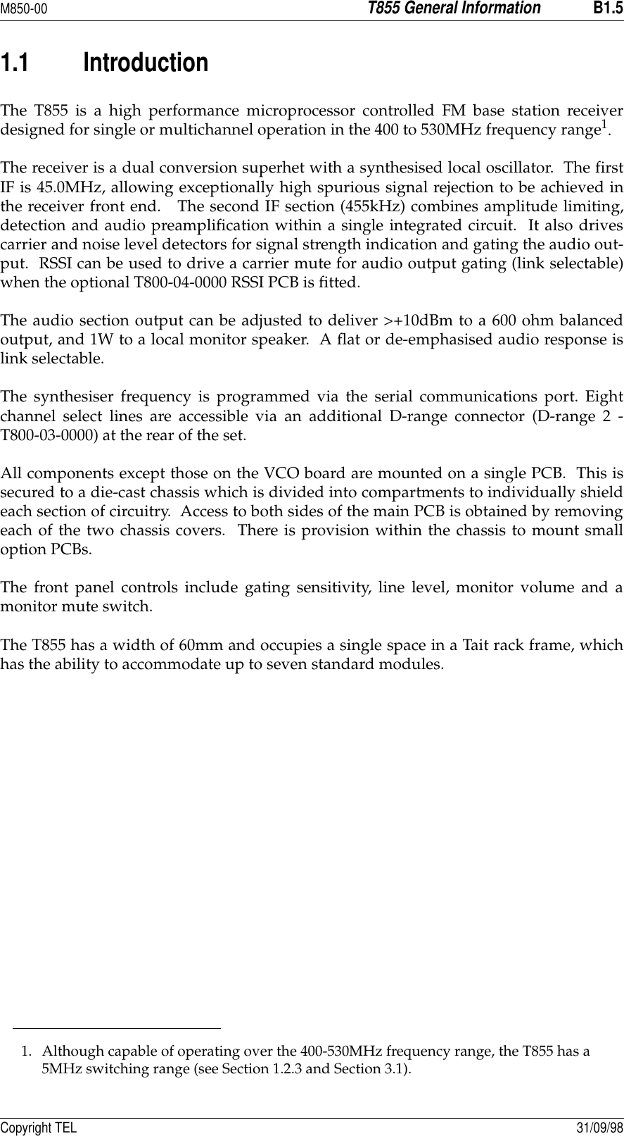

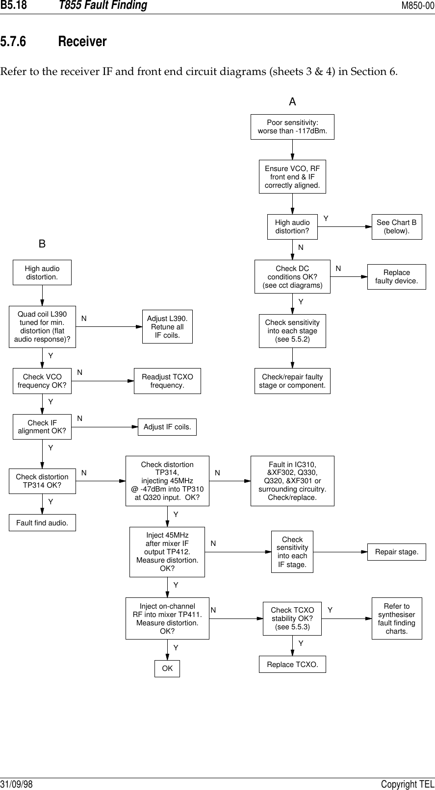
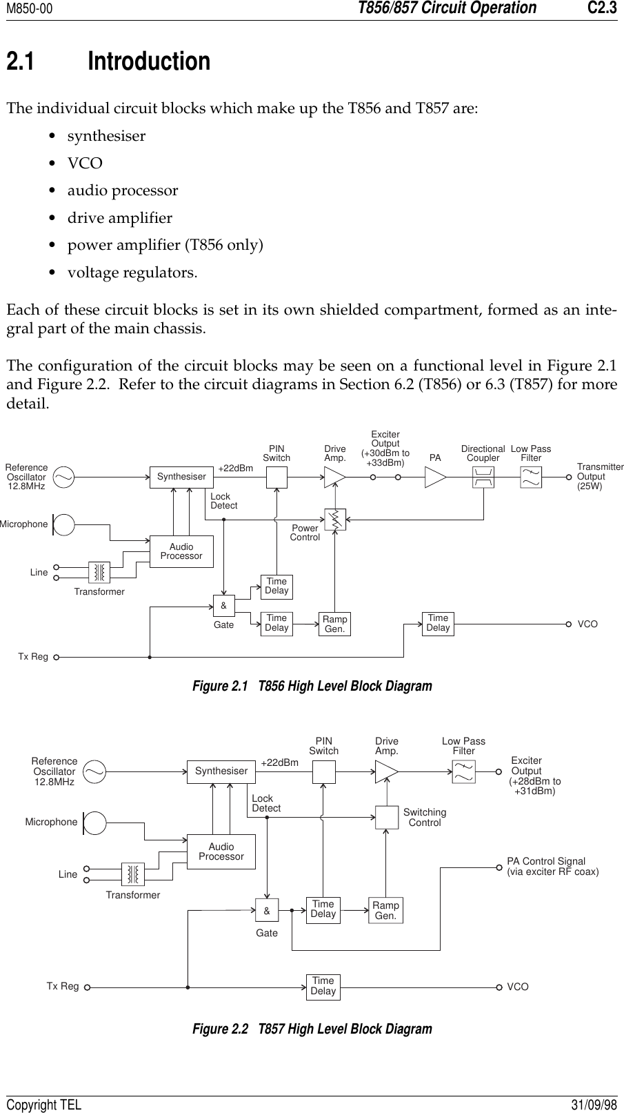
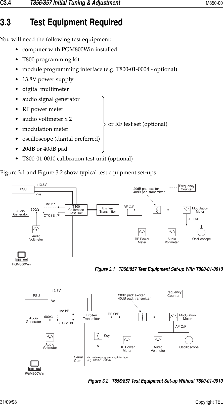
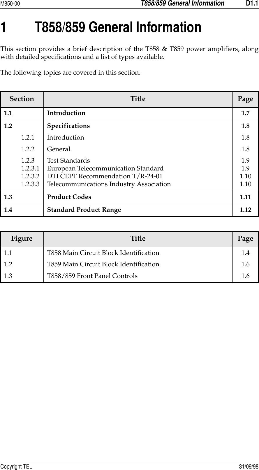
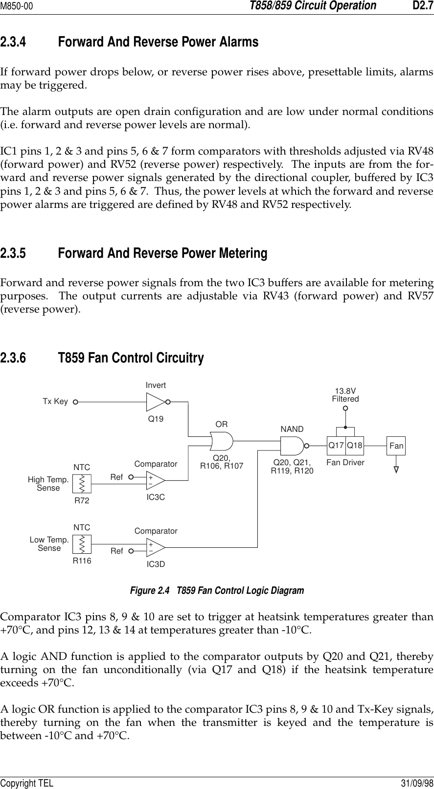
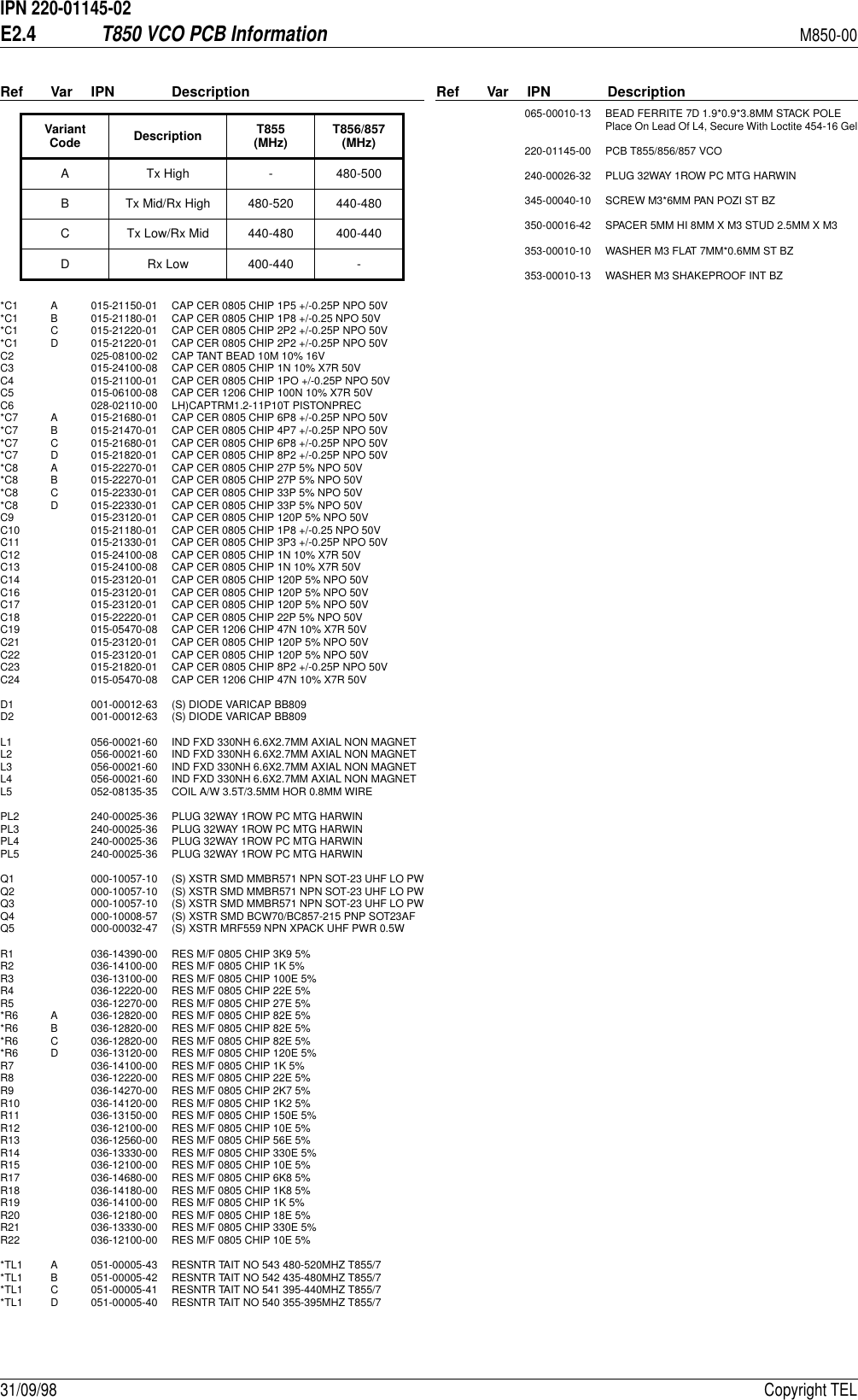
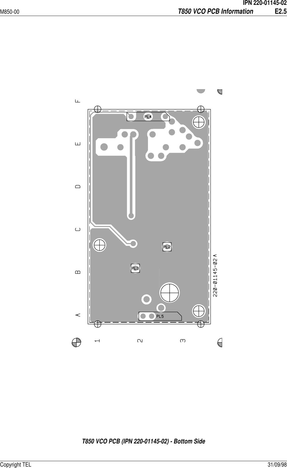
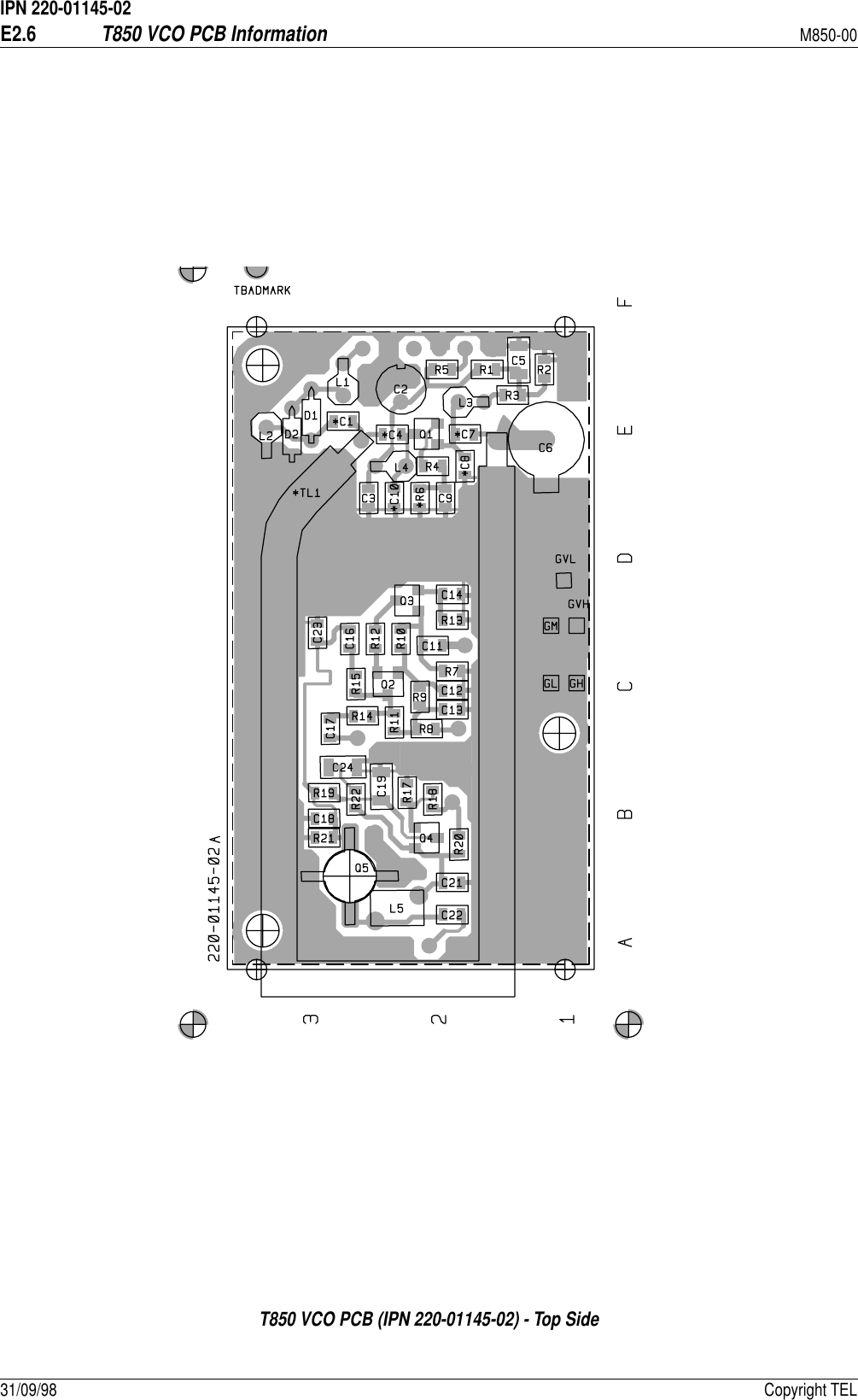
![M850-00T855 Initial Tuning & AdjustmentB3.5Copyright TEL 31/09/983.4 Short Tuning ProcedureUse this procedure only if you want to reprogram the receiver to a frequency outside the5MHz switching range and do not intend to carry out any other major adjustments orrepairs.3.4.1 IntroductionReprogram the operating frequency as described in the PGM800Win program-ming kit (refer to Section 3.2).Remove the top cover (nearest the handle).Set up the test equipment as described in Section 3.3.Set the links in the audio processor section as required (refer to Section 3.5).3.4.2 Synthesiser Alignment• Connect a high impedance voltmeter to the long lead of L1 in the VCO (this meas-ures the synthesiser loop voltage).•Single Channel Tune VCO trimmer C6 for a synthesiser loop voltage of10V.Multichannel Tune VCO trimmer C6 for a synthesiser loop voltage of10V on the middle channel.If there is no middle channel, tune C6 so that the channelsare symmetrically placed around a loop voltage of 10V.All channels should lie within the upper and lower limitsof 16V and 3V respectively.Do not attempt to program channels with a greater fre-quency separation than the specified switching range of5MHz.3.4.3 Front End AlignmentNote 1:In this and following sections deviation settings are given first for widebandwidth sets, followed by settings in brackets for mid bandwidth sets ( )and narrow bandwidth sets [ ].Note 2:For multichannel operation align the receiver on a frequency in the middleof the required band.Inject a strong on-channel RF signal with ±3kHz deviation (±2.4kHz) [±1.5kHz] at1kHz into the antenna socket and adjust the helical resonators #FL410 & #FL420 togive best sinad.](https://usermanual.wiki/Tait/TEL0020/User-Guide-10227-Page-57.png)
![B3.6T855 Initial Tuning & AdjustmentM850-0031/09/98 Copyright TELContinually decrease the RF level to maintain 12dB sinad.Readjust FL410 and FL420 to give best sinad.With PL210 and PL220 connected for de-emphasised audio response, the receiversensitivity should be better than -117dBm, assuming that the audio levels are notbeing overdriven (refer to Section 3.4.5).3.4.4 Mute Adjustment3.4.4.1 Noise MuteConnect pins 1 & 2 of PL250 to enable the noise mute.Set the RF level to -105dBm with ±3kHz deviation (±2.4kHz) [±1.5kHz] at 1kHz.Set RV230 (front panel gating sensitivity) fully anticlockwise.Adjust RV310 (noise mute gain) to close the mute (if necessary turn off the RF sig-nal and then turn it on again).Rotate RV310 anticlockwise until the mute just opens.Adjust RV230 for the required opening sinad.3.4.4.2 Carrier Level MuteConnect pins 2 & 3 of PL250 to enable the carrier mute and disable the noise mute.Apply an on-channel signal from the RF generator at the required mute openinglevel with ±3kHz deviation (±2.4kHz) [±1.5kHz] at ±1kHz.Adjust RV235 (carrier mute) to close the mute (if necessary, momentarily turn offthe RF), then slowly adjust it until the mute just opens. The mute should nowopen at this preset level.3.4.5 Line Amplifier OutputApply an on-channel signal from the RF generator at a level of -70dBm with±3kHz deviation (±2.4kHz) [±1.5kHz] at 1kHz.Adjust RV210 (front panel line level) to set the line level to the required outputlevel.](https://usermanual.wiki/Tait/TEL0020/User-Guide-10227-Page-58.png)
![M850-00T855 Initial Tuning & AdjustmentB3.7Copyright TEL 31/09/983.4.6 CTCSS3.4.6.1 Decoder OperationProgram a CTCSS tone on the set channel using PGM800Win.Set the RF signal generator output to -70dBm.Modulate the generator with:• a 1kHz tone at ±3kHz deviation (±2.4kHz) [±1.5kHz]• a CTCSS tone at the programmed frequency at ±500Hz deviation (±400Hz)[±300Hz].Check that the receiver gate opens and the front panel "Gate" LED is on.3.4.6.2 Opening SinadAdjust RV230 (front panel gating sensitivity) fully clockwise.Reduce the RF signal level to -110dBm.Observe the sinad meter and reduce the RF level until the receiver mute closes.Slowly increase the signal level until the receiver mute just opens and stays open.With PL240 pins 1 & 2 linked (G - H; high pass filter bypassed), check that thesinad is less than 6dB.Reset RV230.3.4.6.3 High Pass FilterSet the audio processor links as follows:Reset the RF signal generator output to -70dBm and note the line level (measure-ment A).Reduce the 1kHz generator to zero output and measure the line level again (meas-urement B).Check that measurement B is at least 30dB below measurement A.Plug Link FunctionPL210 1 - 2 A - B de-emphasised responsePL230 2 - 3 N - P audio from internal CTCSS speech filterPL240 4 - 5 K - L audio input via PL230 or I/O pad](https://usermanual.wiki/Tait/TEL0020/User-Guide-10227-Page-59.png)
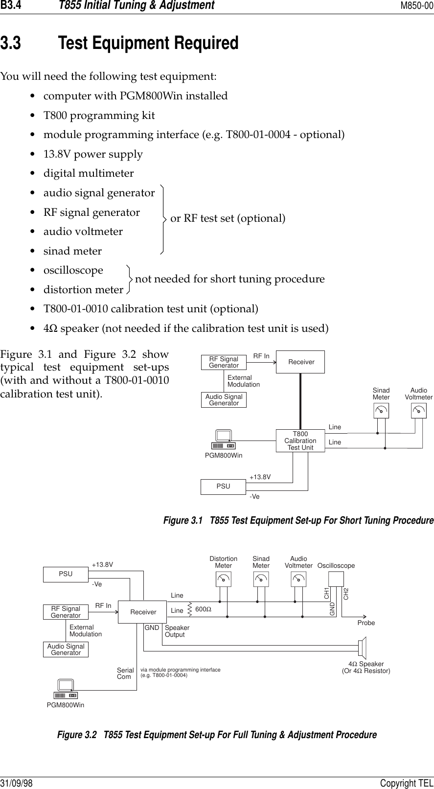
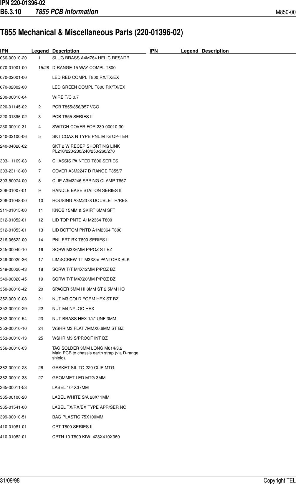
![B3.8T855 Initial Tuning & AdjustmentM850-0031/09/98 Copyright TEL3.4.7 RSSI (If Fitted)The T800-04-0000 RSSI is an optional PCB which adds signal strength monitoring andhigh level mute facilities to the basic receiver.Ensure the T800-04-0000 PCB is fitted in SK320 and SK330 in the IF compartment.Apply an on-channel signal from the RF generator at a level of -100dBm with±3kHz deviation (±2.4kHz) [±1.5kHz] at 1kHz.Adjust RV320 (RSSI level) to give 2.0V RSSI output on pin 5 of D-range 1 (PL100)when measured with a high impedance DMM.3.5 Audio Processor Links3.5.1 GeneralUse the following table to set up the audio processor to the configuration you require.You should set the audio processor links before carrying out the receiver alignment.The factory settings are shown in brackets [ ].Plug Linkaa. The letters in this column and in the table in Section 3.5.2 below refer to the identificationletters screen printed onto the PCB beside each set of pins.FunctionPL210 [1 - 2]2 - 3 [A - B]B - C de-emphasised responseflat responsePL220 1 - 2[2 - 3] D - E[E - F] flat responsede-emphasised responsePL230* 1 - 2[2 - 3]3 - 4M - N[N - P]P - Qaudio input via AUDIO-2 padaudio from internal CTCSS speech filteraudio input via I/O pad P250PL240bb. Refer to Section 3.5.2 for further details.1 - 2[2 - 3]or3 - 44 - 5G - H[H - J]orJ - KK - Lbypass high pass filter300Hz high pass filter in circuitaudio input via PL230 or I/O padPL250 [1 - 2]2 - 3 [R - S]S - T noise mutecarrier mutePL260 1 - 2[2 - 3] U - V[V - W] RX-DISABLE linknot connectedPL270 [1 - 2]2 - 3 [X - Y]Y - Z relay linknot connected](https://usermanual.wiki/Tait/TEL0020/User-Guide-10227-Page-60.png)
![B3.10T855 Initial Tuning & AdjustmentM850-0031/09/98 Copyright TEL3.6 Synthesiser Alignment• Ensure that the receiver has been programmed with the required frequenciesusing the PGM800Win software.• Connect a high impedance voltmeter to the long lead of L1 in the VCO (this meas-ures the synthesiser loop voltage).•Single Channel Tune VCO trimmer C6 for a synthesiser loop voltage of10V.Multichannel Tune VCO trimmer C6 for a synthesiser loop voltage of10V on the middle channel.If there is no middle channel, tune C6 so that the channelsare symmetrically placed around a loop voltage of 10V.All channels should lie within the upper and lower limitsof 16V and 3V respectively.Do not attempt to programme channels with a greater fre-quency separation than the specified switching range of5MHz.• The TCXO =(IC700) output frequency should be trimmed when the IF is tuned -refer to Section 3.7.3.7 Alignment Of Receiver Front End And IFNote:In this and following sections deviation settings are given first for widebandwidth sets, followed by settings in brackets for mid bandwidth sets ( )and narrow bandwidth sets [ ].Align the synthesiser as instructed in Section 3.6. For multichannel operationalign the receiver on a frequency in the middle of the required band.Inject a strong on-channel RF signal with ±3kHz deviation (±2.4kHz) [±1.5kHz] at1kHz into the antenna socket and adjust the helicals (#FL410 and #FL420) to givethe best sinad.Continually decrease the RF level to maintain 12dB sinad.Roughly tune IF coils L310, L320, L330, L340, L350, L360, L370, L380, L385 andL390 for best sinad.While maintaining a low level unmodulated RF input to the receiver, loosely cou-ple into the first IF an additional high level signal at 45MHz - you will hear a beatnote.Trim the synthesiser TCXO (=IC710) for zero beat.While maintaining the low level RF input to the receiver, loosely couple into thesecond IF an additional high level signal at 455kHz - you will hear a beat note.](https://usermanual.wiki/Tait/TEL0020/User-Guide-10227-Page-62.png)
![M850-00T855 Initial Tuning & AdjustmentB3.11Copyright TEL 31/09/98Tune L385 for zero beat.Note:If a second oscillator is not available, you can connect a frequency counter toIC710 pin 8 (i.e. after the TCXO buffer) via an oscilloscope probe to measurethe TCXO frequency directly (12.8MHz). At this point the voltage level isapproximately 4V p-p.Readjust the front end helicals (#FL410 and #FL420) to give the best sinad.Change the RF signal level to -75dBm and modulate with ±3kHz deviation(±2.4kHz) [±1.5kHz] at 1kHz.Connect an oscilloscope probe to SK320 pin 3 (RSSI 455kHz input) and connectplugs PL210 and PL220 to give a flat audio response (refer to Section 3.5).Readjust L310, L320, L330, L340, L350, L360, L370 and L380 to give a maximumamplitude response on the oscilloscope with minimal amplitude modulation. Note:If you would like a more accurate method of tuning the IF, refer to the sweeptuning method described in Section 5.5.5.Further adjust these coils, along with L390, for minimum audio distortion, ensur-ing that the 455kHz level (on the oscilloscope) does not fall significantly.Check that the distortion reading is:wide bandwidth ≤2%mid and narrow bandwidth ≤4%.If required, reconnect plugs PL210 and PL220 to give a de-emphasised audioresponse and check that the distortion reading is ≤2% (all bandwidths).Reduce the RF level until 12dB sinad is reached. The receiver sensitivity shouldbe better than -117dBm (de-emphasised) or -111dBm (flat), assuming that theaudio levels are not being overdriven (refer to Section 3.11).](https://usermanual.wiki/Tait/TEL0020/User-Guide-10227-Page-63.png)
![B3.12T855 Initial Tuning & AdjustmentM850-0031/09/98 Copyright TEL3.8 Gating DelayTwo solder links (SL210 & SL220) are provided on the bottom of the PCB to allow threegate delay time options, as shown in the table below.*Factory setting.3.9 Noise Mute AdjustmentConnect pins 1 & 2 of PL250 to enable the noise mute.Align the receiver as instructed in Section 3.6 and Section 3.7.Set the RF level to -105dBm with ±3kHz deviation (±2.4kHz) [±1.5kHz] at 1kHz.Set RV230 (front panel gating sensitivity) fully anticlockwise.Adjust RV310 (noise mute gain) to close the mute (if necessary turn off the RF sig-nal and then turn it on again).Rotate RV310 anticlockwise until the mute just opens.Once the mute has been set up as described above, adjust RV230 for the required open-ing sinad.3.10 Carrier Level MuteConnect pins 2 & 3 of PL250 to enable the carrier mute and disable the noise mute.Apply an on-channel signal from the RF generator at the required mute openinglevel with ±3kHz deviation (±2.4kHz) [±1.5kHz] at ±1kHz.Adjust RV235 (carrier mute) to close the mute (if necessary, momentarily turn offthe RF), then slowly adjust it until the mute just opens. The mute should nowopen at this preset level.SL210 SL220 Closing Delaylinked not linked <50ms*not linked linked <25msnot linked not linked <20ms](https://usermanual.wiki/Tait/TEL0020/User-Guide-10227-Page-64.png)
![M850-00T855 Initial Tuning & AdjustmentB3.13Copyright TEL 31/09/983.11 Audio Processor3.11.1 Line Amplifier OutputApply an on-channel signal from the RF generator at a level of -70dBm with±3kHz deviation (±2.4kHz) [±1.5kHz] at 1kHz.Adjust RV210 (front panel line level) to give an output of +10dBm on the 600 ohmline.Check for any clipping or distortion on the oscilloscope.Set the line level to the required output level.3.11.2 Monitor Amplifier Output (Speaker Output)Adjust RV205 (front panel monitor volume) to give an output of 2V rms into a 4ohm resistive load.Check for any clipping or distortion on the oscilloscope.Switch to a 4 ohm speaker and adjust RV205 to the required level.3.12 CTCSS3.12.1 Decoder OperationProgram a CTCSS tone on the set channel using PGM800Win.Set the RF signal generator output to -70dBm.Modulate the generator with:• a 1kHz tone at ±3kHz deviation (±2.4kHz) [±1.5kHz]• a CTCSS tone at the programmed frequency at ±500Hz deviation (±400Hz)[±300Hz].Check that the receiver gate opens and the front panel "Gate" LED is on.3.12.2 Opening SinadAdjust RV230 (front panel gating sensitivity) fully clockwise.Reduce the RF signal level to -110dBm.](https://usermanual.wiki/Tait/TEL0020/User-Guide-10227-Page-65.png)
![B3.14T855 Initial Tuning & AdjustmentM850-0031/09/98 Copyright TELObserve the sinad meter and reduce the RF level until the receiver mute closes.Slowly increase the signal level until the receiver mute just opens and stays open.With PL240 pins 1 & 2 linked (G - H; high pass filter bypassed), check that thesinad is less than 6dB.Reset RV230.3.12.3 High Pass FilterSet the audio processor links as follows:Reset the RF signal generator output to -70dBm and note the line level (measure-ment A).Reduce the 1kHz generator to zero output and measure the line level again (meas-urement B).Check that measurement B is at least 30dB below measurement A.3.13 RSSIThe T800-04-0000 RSSI is an optional PCB which adds signal strength monitoring andhigh level mute facilities to the basic receiver.Ensure the T800-04-0000 PCB is fitted in SK320 and SK330 in the IF compartment.Align the receiver as instructed in Section 3.6 and Section 3.7.Apply an on-channel signal from the RF generator at a level of -100dBm with±3kHz deviation (±2.4kHz) [±1.5kHz] at 1kHz.Adjust RV320 (RSSI level) to give 2.0V RSSI output on pin 5 of D-range 1 (PL100)when measured with a high impedance DMM.Plug Link FunctionPL210 1 - 2 A - B de-emphasised responsePL230 2 - 3 N - P audio from internal CTCSS speech filterPL240 4 - 5 K - L audio input via PL230 or I/O pad](https://usermanual.wiki/Tait/TEL0020/User-Guide-10227-Page-66.png)
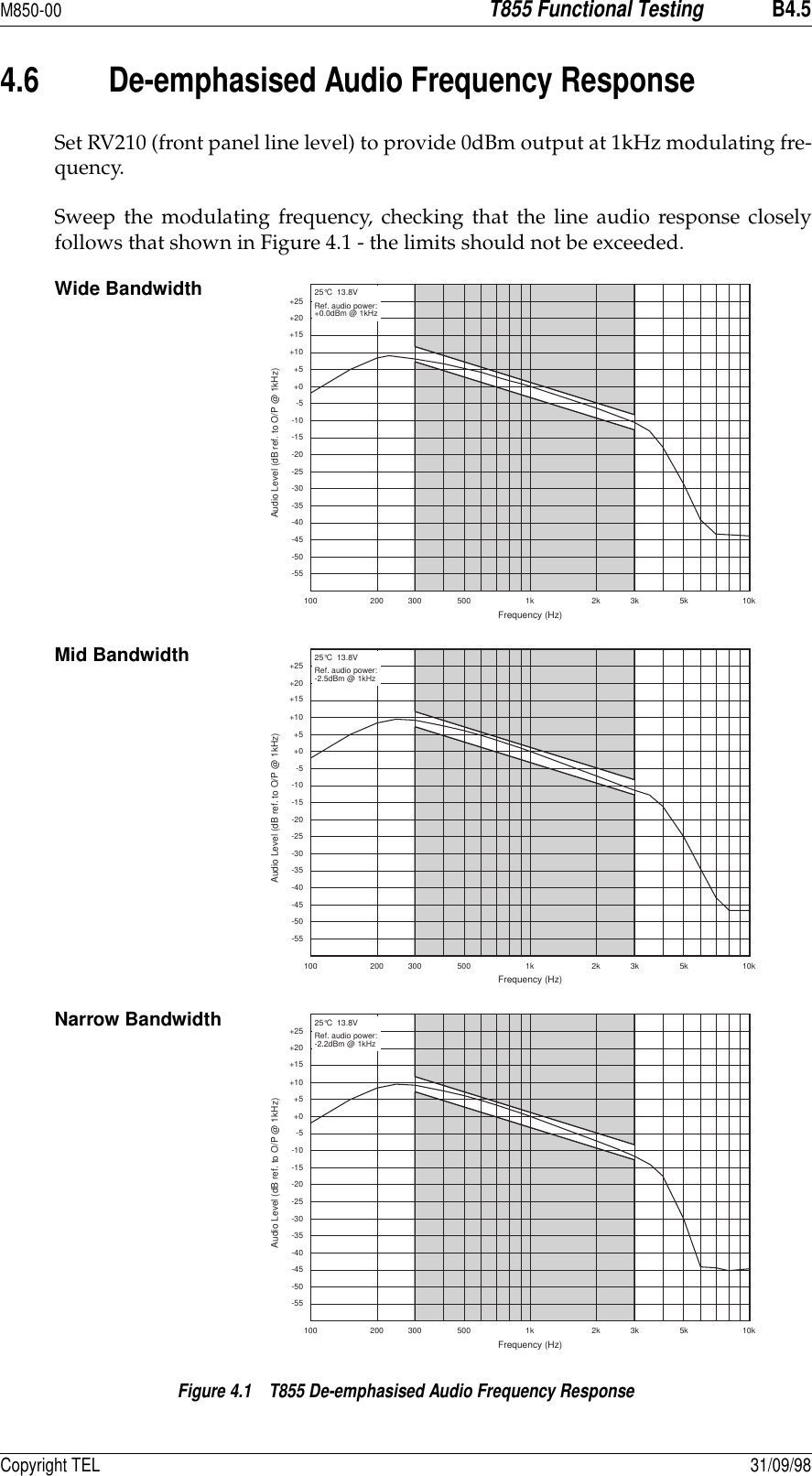
![M850-00T855 Functional TestingB4.1Copyright TEL 31/09/984 T855 Functional TestingCaution:This equipment contains CMOS devices which are susceptible to dam-age from static charges. Refer to Section 1.2 in Part A for more infor-mation on anti-static procedures when handling these devices.The following test procedures will confirm that the T855 has been tuned and adjustedcorrectly and is fully operational.Note 1:In this and following sections deviation settings are given first for widebandwidth sets, followed by settings in brackets for mid bandwidth sets ( )and narrow bandwidth sets [ ].Note 2:Unless otherwise specified, the term "PGM800Win" used in this and follow-ing sections refers to version 2.00 and later of the software.Refer to Figure 4.3 for the location of the main tuning and adjustment controls, and toSection 3.3 for the test equipment set-up. Refer also to Section 6 where the parts lists,grid reference index and diagrams will provide detailed information on identifying andlocating components and test points on the main PCB. The parts list and diagrams forthe VCO PCB are in Part E.The following topics are covered in this section.Section Title Page4.1 Current Consumption 4.34.2 Sensitivity 4.34.3 Switching Range 4.34.4 Audio Distortion 4.44.5 Ultimate Signal-To-Noise Ratio 4.44.6 De-emphasised Audio Frequency Response 4.54.7 Noise Mute (If Linked In) 4.64.8 RSSI (If Fitted) 4.64.9 Carrier Level Mute (RSSI Fitted & Carrier Mute Linked In) 4.7Figure Title Page4.14.24.3T855 De-emphasised Audio Frequency ResponseT855 RSSI Voltage vs Signal StrengthT855 Main Tuning & Adjustment Controls4.54.64.9](https://usermanual.wiki/Tait/TEL0020/User-Guide-10227-Page-67.png)

![M850-00T855 Functional TestingB4.3Copyright TEL 31/09/984.1 Current ConsumptionConnect the T855 to a 13.8V power supply.Rotate RV230 (front panel gating sensitivity) anticlockwise until the "Gate" LED isextinguished.Set switch SW201 (front panel monitor mute) to the on position.Check that the current in the 13.8V power cable is less than 350mA.Rotate the RV230 clockwise until the "Gate" LED is lit.Rotate RV210 (front panel line level) and RV205 (front panel monitor volume) togive maximum outputs.Check that the current is less than 750mA.Reset the front panel controls to the required settings.4.2 SensitivityIf CTCSS is enabled, disable the CTCSS tone by either programming the T855 for"No Tone" on the set channel, or by pulling pin 10 of D-range 2 (CTCSS ENABLE)low.Apply an on-channel signal from the RF generator with ±3kHz deviation(±2.4kHz) [±1.5kHz] at 1kHz.Adjust the RF level to give 12dB audio sinad.Check that the sensitivity is -117dBm or better.4.3 Switching Range Apply an on-channel signal from the RF generator at various frequencies withinthe 5MHz switching range (front end bandwidth), corresponding to pre-pro-grammed channels.Measure the sensitivity at each frequency as described in Section 4.2.Ensure that the sensitivity is -115dBm or better across the whole switching range.](https://usermanual.wiki/Tait/TEL0020/User-Guide-10227-Page-69.png)
![B4.4T855 Functional TestingM850-0031/09/98 Copyright TEL4.4 Audio DistortionThe level of distortion measured at the line output (refer to Figure 1.3 in Part F) gives anindication of the accuracy of the IF alignment.Apply an accurate on-channel signal from the RF generator at a level of -70dBmwith ±3kHz deviation (±2.4kHz) [±1.5kHz] at 1kHz.Adjust RV210 (front panel line level) to give +10dBm into 600 ohms.Check that the distortion is approximately 1% THD.Note:For a flat response, the distortion should always be better than 2% for widebandwidth sets or 4% for mid and narrow bandwidth sets.Adjust RV205 (front panel monitor volume) to give 2V rms into a 4 ohm resistiveload.Check that the distortion at the monitor output is better than 2% THD.Reset the controls before proceeding to the next set of tests.4.5 Ultimate Signal-To-Noise RatioApply a signal from the RF generator at a level of -57dBm with ±3kHz deviation(±2.4kHz) [±1.5kHz] at 1kHz.Select de-emphasis on the links provided in the audio processor (refer to Section3.5), and link pins 2 & 3 of PL240 to include the 300Hz filter.Adjust RV210 (front panel line level) to provide +10dBm output.Switch off the modulation, checking that the residual noise is lower than -45dBm(-43dBm) [-39dBm] at the line output (this corresponds to S/N of 55dB (53dB)[49dB] and is in accordance with EIA measurement conditions).Note:You can make the measurement without the 300Hz high pass filter, but theresult will be 10dB worse.](https://usermanual.wiki/Tait/TEL0020/User-Guide-10227-Page-70.png)
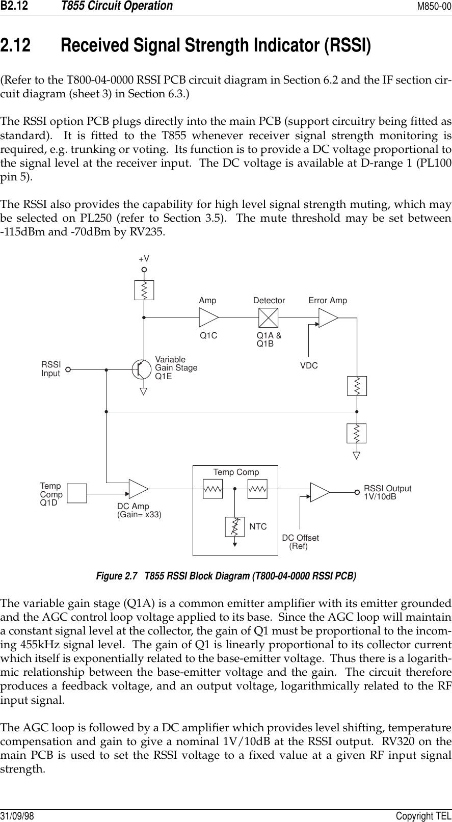
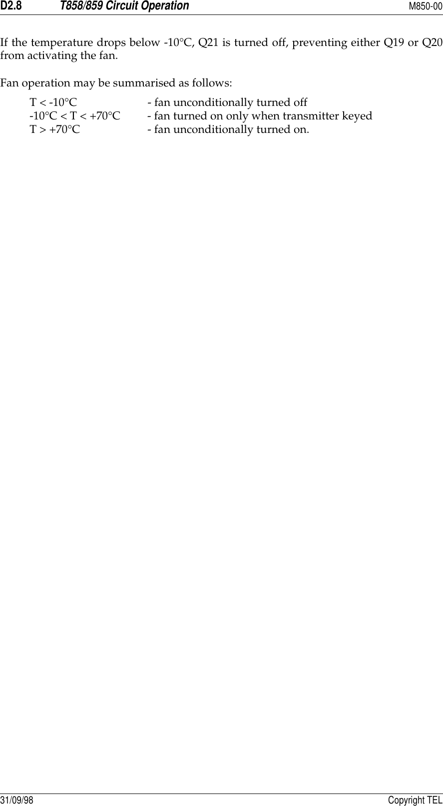
![B4.6T855 Functional TestingM850-0031/09/98 Copyright TEL4.7 Noise Mute (If Linked In)Rotate RV230 (front panel gating sensitivity) fully anticlockwise.Apply an on-channel signal from the RF generator at a level of -110dBm with±3kHz deviation (±2.4kHz) [±1.5kHz] at 1kHz.Increase the RF level in 1dB steps, checking that the mute opens for an RF inputlevel of approximately -105dBm.Turn the RF off and check that the mute closes.Rotate RV230 clockwise and check that the mute opens.Reset RV230 to give the required opening sinad.Caution:Some RF generators can cause a false opening of the mute because thegenerator produces a burst of noise when the attenuation rangechanges. To correct the problem you will have to change generators. 4.8 RSSI (If Fitted)Apply an on-channel signal from the RF generator at a level of -110dBm with±3kHz deviation (±2.4kHz) [±1.5kHz] at 1kHz.Using a high impedance DMM, check that the RSSI output voltage on pin 5 ofD-range 1 (PL100) is 2V (nominal).Vary the RF level in 5dB steps and check that the RSSI output voltage changes at arate of approximately 10dB/V over the range of -115dBm to -70dBm (refer to Fig-ure 4.2 for RSSI voltage vs signal strength).Figure 4.2 T855 RSSI Voltage vs Signal StrengthRF Level (dBm)-130 -120 -110 -100 -90 -80 -70 -6012345678RSSI Voltage](https://usermanual.wiki/Tait/TEL0020/User-Guide-10227-Page-72.png)
![M850-00T855 Functional TestingB4.7Copyright TEL 31/09/984.9 Carrier Level Mute (RSSI Fitted & Carrier Mute Linked In)Apply an on-channel signal from the RF generator at a level of -120dBm with±3kHz deviation (±2.4kHz) [±1.5kHz] at 1kHz.Increase the RF level in 2dB steps and check that the mute opens at an RF levelwhich corresponds with the preset level on RV235 (carrier mute), i.e. between-115dBm and -70dBm.](https://usermanual.wiki/Tait/TEL0020/User-Guide-10227-Page-73.png)
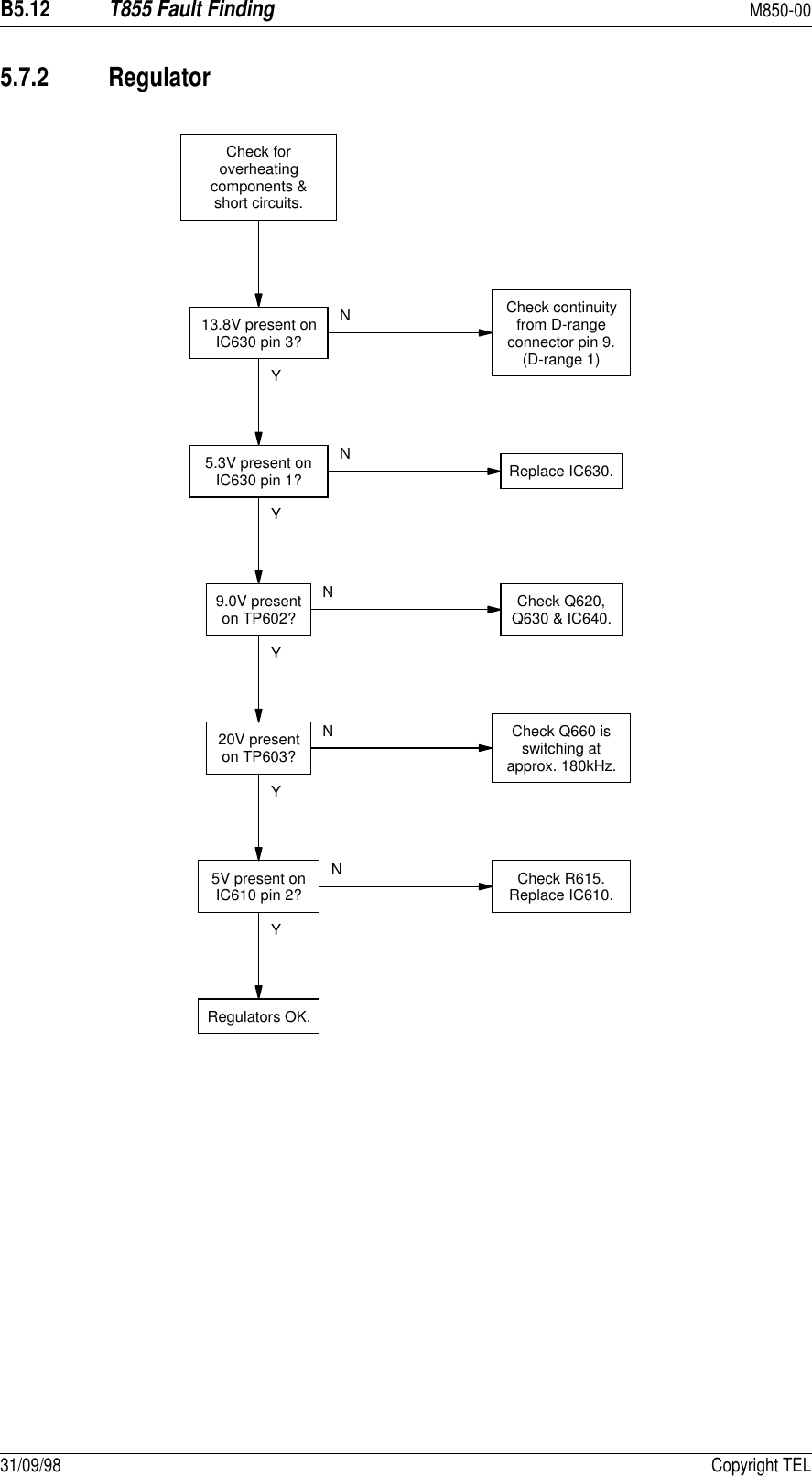
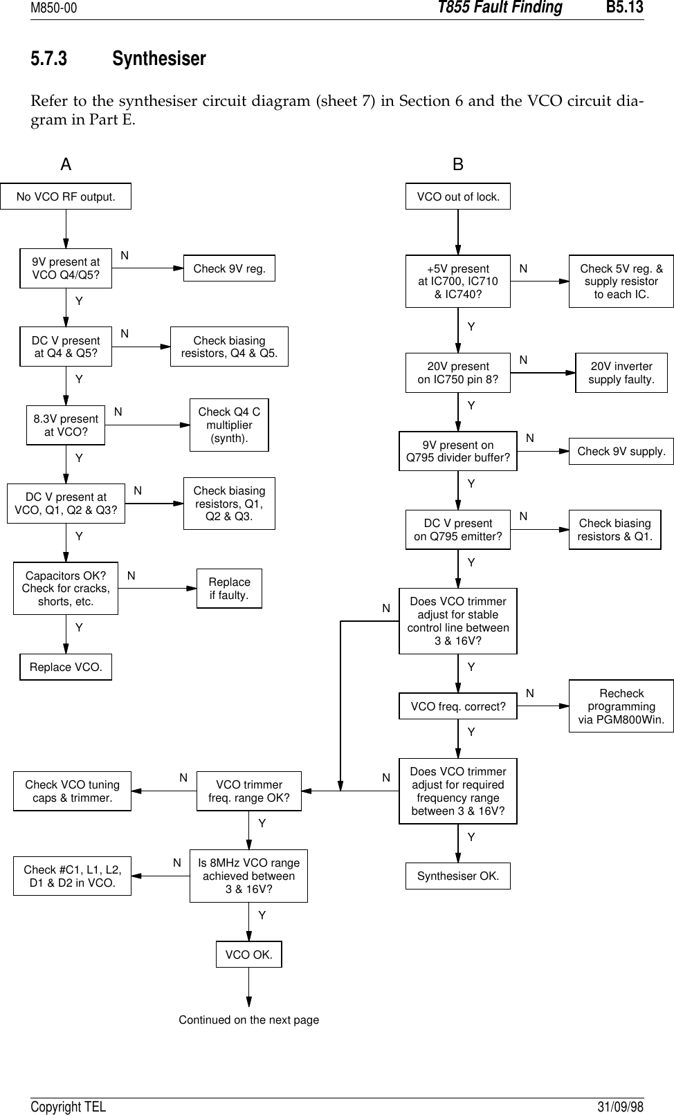
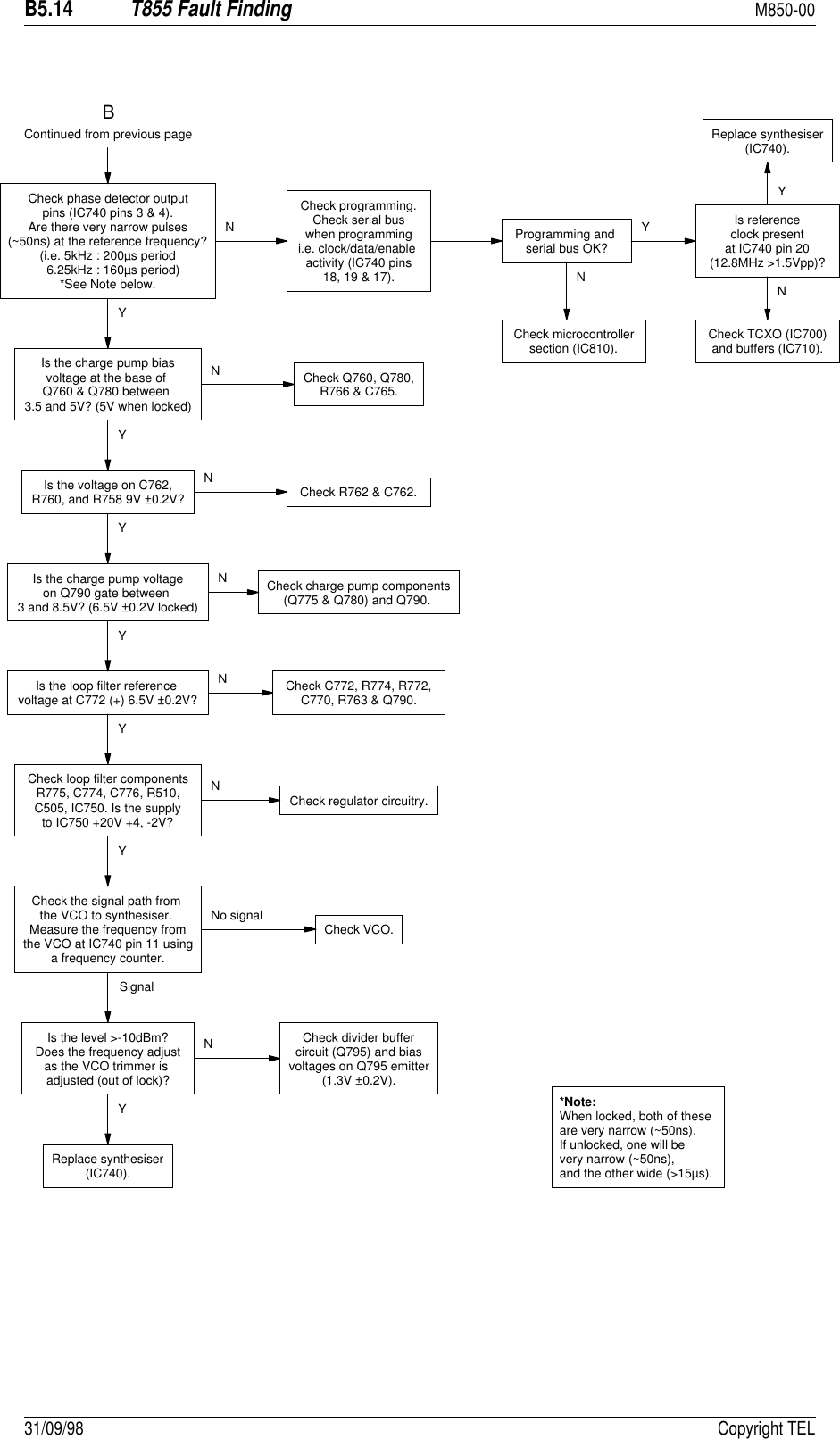
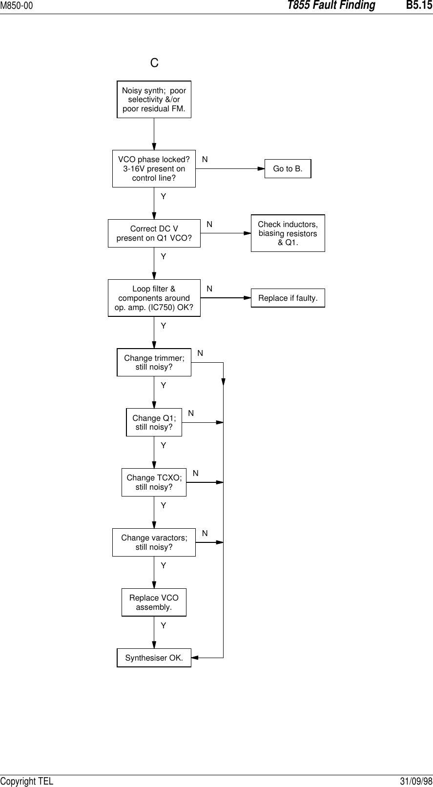
![M850-00T855 Fault FindingB5.1Copyright TEL 31/09/985 T855 Fault FindingCaution:This equipment contains CMOS devices which are susceptible to dam-age from static charges. Refer to Section 1.2 in Part A for more infor-mation on anti-static procedures when handling these devices.The following test procedures and fault finding flow charts may be used to help locate ahardware problem, however they are by no means a complete fault finding procedure.If you still cannot trace the fault after progressing through them in a logical manner,contact your nearest Tait Dealer or Customer Service Organisation. If necessary, you canget additional technical help from Customer Support, Radio Systems Division, Tait Elec-tronics Ltd, Christchurch, New Zealand (full contact details are on page 2).Note 1:In this and following sections deviation settings are given first for widebandwidth sets, followed by settings in brackets for mid bandwidth sets ( )and narrow bandwidth sets [ ].Note 2:Unless otherwise specified, the term "PGM800Win" used in this and follow-ing sections refers to version 2.00 and later of the software.Refer to Section 6 where the parts lists, grid reference index and diagrams will providedetailed information on identifying and locating components and test points on themain PCB. The parts list and diagrams for the VCO PCB are in Part E.The following topics are covered in this section.Section Title Page5.1 Visual Checks 5.35.2 Component Checks 5.35.3 Front Panel LED Indicator 5.35.45.4.15.4.25.4.3DC ChecksPower RailsVCO LockingMute Operation5.45.45.45.45.55.5.15.5.25.5.35.5.3.15.5.3.25.5.45.5.5RF ChecksVCO FrequencyRF SensitivityOscillator StabilityTCXOSecond IFDemodulator OutputIF Distortion5.55.55.55.65.65.65.65.6](https://usermanual.wiki/Tait/TEL0020/User-Guide-10227-Page-75.png)
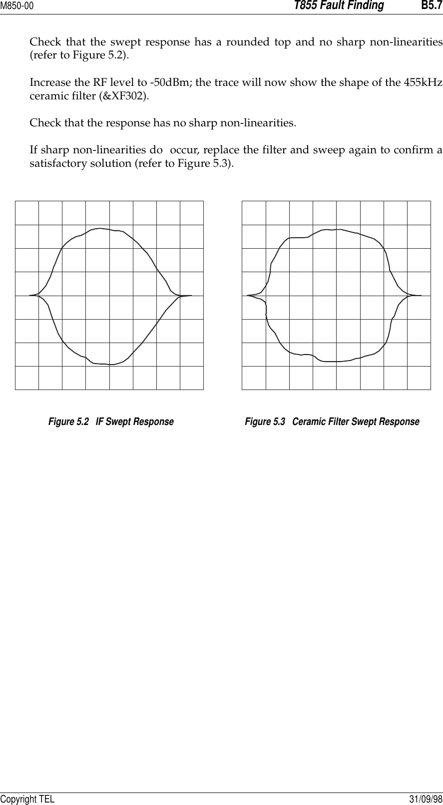
![B5.6T855 Fault FindingM850-0031/09/98 Copyright TEL5.5.3 Oscillator Stability5.5.3.1 TCXOWhile maintaining a low level unmodulated RF input to the receiver, loosely cou-ple into the first IF an additional high level signal at 45MHz - you should nowhear a constant low frequency beat note.Tap the TCXO with a finger and replace it if the beat note permanently changes.5.5.3.2 Second IFWhile maintaining a low level unmodulated RF input to the receiver, loosely cou-ple into the second IF an additional high level signal at 455kHz - you should nowhear a constant low frequency beat note.Adjust L385 for "zero beat".5.5.4 Demodulator OutputApply an on-channel RF signal modulated by 1kHz with ±3kHz (±2.4kHz)[±1.5kHz] deviation at an amplitude of -65dBm.Connect an oscilloscope probe (DC coupled) to TP314 (audio output).Check that an audio signal of approximately 800mV peak to peak is present.Optimum tuning of the quad coil (L390) for minimum audio distortion (with a "flat"audio response) should coincide with maximum audio amplitude and a DC level ofapproximately 1.7V.5.5.5 IF DistortionIf the audio distortion is still high after careful IF alignment (Section 3.7), sweep the IF toinvestigate the bandpass response.Apply an on-channel RF signal modulated at 10Hz with ±12kHz (±9kHz) [±6kHz]deviation at an amplitude of -80dBm.Connect the modulating 10Hz audio signal to the "X" input of an oscilloscope andobserve the 455kHz IF input to SK320 pin 3 via a suitable RF probe on the "Y"input. Alternatively, if you have an RSSI PCB fitted, use an oscilloscope probe forthe "Y" input to monitor the RSSI output voltage at pad P238 (RSSI test point) orpin 5 of D-range 1 (PL100). This will give a demodulated log response and onlythe top half of the wave forms shown in Figure 5.2 and Figure 5.3 will be dis-played on the oscilloscope screen.Note:The "X" input should be DC coupled.](https://usermanual.wiki/Tait/TEL0020/User-Guide-10227-Page-80.png)
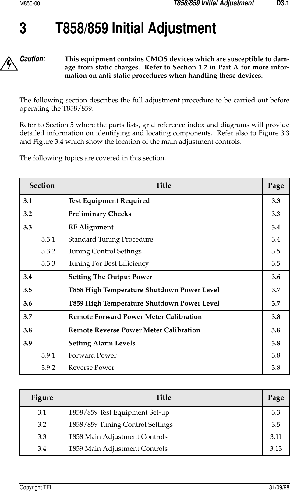
![B5.16T855 Fault FindingM850-0031/09/98 Copyright TEL5.7.4 Noise MuteRefer to audiofault finding chart.Ensure PL250 is setfor noise mute operation.Check Q340& Q350.Check D310 isrectifying noise.Vary RF level &observe voltageon pad 236.Pad 236 voltagevaries 0-1.8V?Check 9V rail &resistors R264,R265 & R284.Replace IC270.Check/replaceIC270 & D240.Replace Q250.NYNYNYYNYYYYNRefer toreceiver faultfinding chart.Check componentsaround active filter.Mutable audioon outputs?YVoltage varies0-2.5V?NOKDoes "Gate" LEDtoggle on/off?NCheck Q230, Q245 &Q290 for operation.YAdjust RV230(gating sensitivity)& observe voltageon IC270 pin 3.Set RF signal level to-117dBm. RotateRV230 c/w & cc/w.Monitor voltage onIC270 pin 1. Switching0-8V as RV230 rotated?Monitor voltage onIC270 pin 7. Switching0-8V as RV230 rotated?Monitor voltage onpad 234. Switching0-8V as RV230 rotated?NNNDoes "Gate"LED toggle? Check/replaceQ255 & D250.YYNCheck RV330adjustment(noise mute gain).Approx. 0.6V DC rect-ified noise on pad 236?NSwitch SW201 (monitormute) to ensuremute is enabled.Rotate RV230(gating sensitivity)c/w & cc/w & view"Gate" LED.Note:c/w = clockwisecc/w = counterclockwise or anticlockwiseAudio onTP314?Noise onIC310 pin 11?Amplified noiseon C380?Apply on channel signal@ -117dBm* to receiver. *Modulated by 1kHz signal with ±3kHz (±2.4kHz) [±1.5kHz] deviation](https://usermanual.wiki/Tait/TEL0020/User-Guide-10227-Page-90.png)
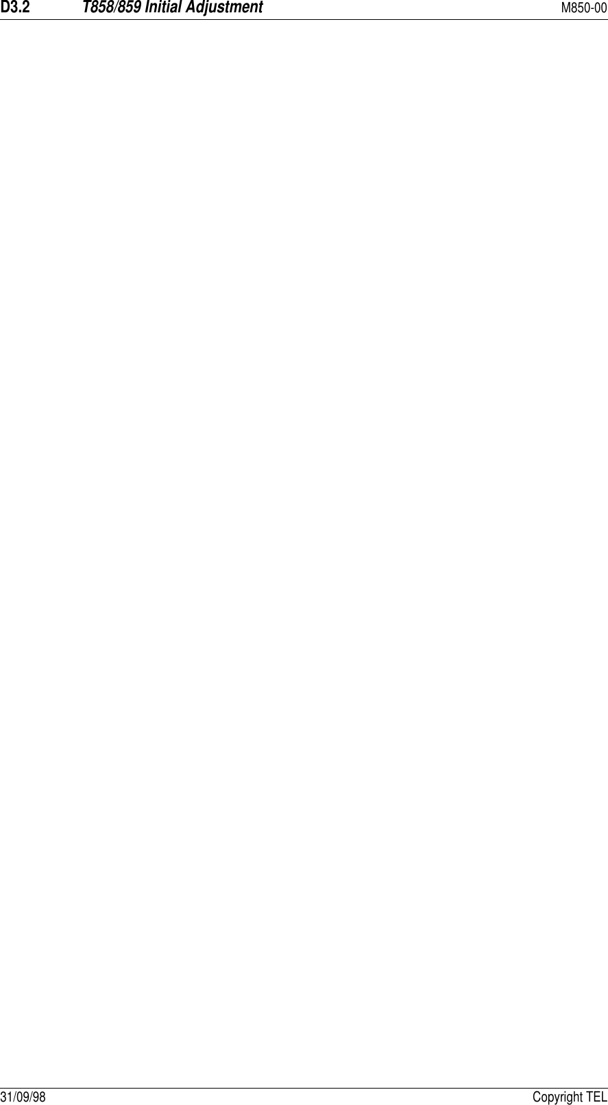
![M850-00T855 Fault FindingB5.17Copyright TEL 31/09/985.7.5 Carrier Mute Approx. 5V onRSSI pad 238?Approx. 5V onIC280 pin 1? Check/replace IC280& adjoining components.Check Q230, Q245 &Q290 for operation. Adjust RV235 &observe voltageon IC280 pin 6.Switch SW201(monitor mute) to ensuremute is enabled.YNNNYYDoes "Gate" LEDtoggle on/off?Refer to receiver faultfinding chart.NYYVoltage varies0-6V?Check 9V rail &resistors R275,R277 & RV235.YNSet RF signal levelto -95dBm. RotateRV235 c/w & cc/w.Monitor voltage onIC280 pin 7. Switching0-8V as RV235 rotated? Replace IC280.NYMonitor voltage onIC270 pin 7. Switching0-8V as RV235 rotated?Check/replaceIC270 & D240.NYMonitor voltage onpad 234. Switching0-8V as RV235 rotated? Replace Q250.NYDoes "Gate"LED toggle? Check/replaceQ255 & D250.YNMutable audioon outputs?OKNYRefer to audiofault finding chart.Note:c/w = clockwisecc/w = counterclockwise or anticlockwiseRotate RV235(carrier mute) c/w & cc/w& view "Gate" LED.Apply on channel signal@ -110dBm* to receiver.Audio onTP314?*Modulated by 1kHz signal with ±3kHz (±2.4kHz) [±1.5kHz] deviation.Approx. 2V atD-Range 1 pin 5?NEnsure PL250 is setfor carrier mute operation,and the RSSI PCB is fitted.Check for short circuitsand/or replace IC310.Check Q340 andadjoining components.](https://usermanual.wiki/Tait/TEL0020/User-Guide-10227-Page-91.png)
![M850-00T855 Fault FindingB5.19Copyright TEL 31/09/985.7.7 Audio Audio onIC210 pin 1? Check componentsaround IC210.Apply on channel signal@ -117dBm* to receiver.Refer toreceiver faultfinding chart.Ensure RV230(gating sensitivity)fully clockwise."Gate" LED on? Refer to mutefault finding charts.YNNYNYNYAudio onspeaker?Audio onC238/C259?Audio onIC240 pin 2 &IC260 pin 2?Replace C249 &check continuity.Audio on linemonitor (pad 284)& line output?Refer to mutefault finding charts.OKCheck/replaceoutput components.NYNYNYNYAudio onTP314?Audio attop of RV205& RV210?Check C233.Check link PL240.Replacefaulty IC.*Modulated by 1kHz signal with ±3kHz (±2.4kHz) [±1.5kHz] deviation.](https://usermanual.wiki/Tait/TEL0020/User-Guide-10227-Page-93.png)


![M850-00T856/857 General InformationC1.11Copyright TEL 31/09/981.2.4.2 Modulation CharacteristicsFrequency Response .. flat or pre-emphasised (optional) (below limiting)Line And Microphone Inputs: Pre-emphasised Response- Bandwidth .. 300Hz to 3kHz (WB & MB).. 300Hz to 2.55kHz (NB)Below Limiting .. within +1, -3dB of a 6dB/octavepre-emphasis characteristic Flat Response .. within +1, -2dB of output at 1kHzAbove Limiting Response .. within +1, -2dB of a flat response(ref. 1kHz)Distortion .. 2%Hum And Noise: Wide Bandwidth .. -55dB (300Hz to 3kHz [EIA]) typical Mid Bandwidth .. -55dB (CEPT)Narrow Bandwidth .. -50dB (CEPT) Compressor (optional): Attack Time .. 10ms Decay Time .. 800ms Range .. 50dB1.2.4.3 CTCSSStandard Tones .. all 37 EIA group A, B and C tonesplus 13 commonly used tonesFrequency Error .. 0.08% max.(from EIA tones)Generated Tone Distortion .. 1.2% max.Generated Tone Flatness .. flat across 67 to 250.3Hz to within 1dBModulation Level .. adjustableModulated Distortion .. <5%1.2.5 MicrocontrollerAuxiliary Ports:Open Drain Type .. capable of sinking 2.25mA via 2k2ΩVds max. .. 5V](https://usermanual.wiki/Tait/TEL0020/User-Guide-10227-Page-135.png)


![M850-00T856/857 Circuit OperationC2.9Copyright TEL 31/09/982.5.3 Keying InputsThere are four ways to key the exciter: • pulling the Tx-Key line low (pin 13 on D-range 1 [PL100]) at the rear of the set);• pushing the "Carrier" button on the front panel - this will inhibit all audio;• using the PTT button on the local microphone, disabling audio from the line;• via the opto-key inputs (pins 11 and 12 on D-range 1 [PL100]) when electricalisolation is required. This features a constant current sink (Q270) to ensure reli-able activation of the opto-coupler (IC250) at low keying voltages.2.5.4 Compressor (Automatic Level Control (ALC))The input signal is fed via a current controlled attenuator (Q230, Q220) to a high gainstage (IC230) from which the output signal is taken. This signal is passed to a compara-tor (IC230) which toggles whenever the audio signal exceeds a DC threshold deter-mined by RV220. Thus, the comparator produces a square wave whose mark-spaceratio is determined by the amplitude of the audio signal. This square wave pumps upthe reservoir capacitor (C233) which controls the attenuator (Q230, Q220), thus complet-ing the feedback loop.The compression level is set by adjustment of the comparator threshold (RV220).Note:Although the high dynamic range of the compressor allows the use of verylow audio signal levels, such conditions will be accompanied by a degrada-tion of the signal-to-noise ratio. Very low audio input levels should there-fore be avoided where possible.2.5.5 Outputs To ModulatorsThe output signal from the limiter (IC210, IC230) is summed with a CTCSS tone at asumming amplifier (IC260). The signal is then low pass filtered (IC260) and split to sup-ply the two modulators.Since the VCO modulator is a true frequency modulator, its audio is simply buffered(IC260). The reference modulator, however, is a phase modulator and its audio mustfirst be integrated (IC210).It is vital that the audio levels to the modulators are accurately set, relative to eachother. Hence the inclusion of level adjustment in the reference modulator path. Onceset, adjustments to absolute deviation may be made only via the deviation digital pot.(IC220 - adjustable via PGM800Win).](https://usermanual.wiki/Tait/TEL0020/User-Guide-10227-Page-149.png)

![C3.6T856/857 Initial Tuning & AdjustmentM850-0031/09/98 Copyright TEL3.4.4 Two Point Modulation AdjustmentNote 1:In this and following sections deviation settings are given first for widebandwidth sets, followed by settings in brackets for mid bandwidth sets ( )and narrow bandwidth sets [ ].Note 2:Reference modulation and limiter adjustment are controlled byPGM800Win. Electronic potentiometers (256 step) are used to allow chan-nel-by-channel adjustment of deviation and two point modulation.Note 3:To optimise the modulation response across the switching range, repeatsteps 1-4 below for each channel that will be used (usually needed only fordata applications). In applications where the modulation response is lesscritical (e.g. voice use only), carry out steps 1-4 below on the middle channeland cut and paste the value to all other channels.1. Inject an audio signal of 300Hz 1.5V rms (+5dBm) into the CTCSS input (D-range1 (PL100) pin 8). Key the transmitter by earthing the Tx-Key line.2. Adjust the output from the audio generator to obtain ±3kHz (±2.4kHz) [±1.5kHz]deviation at 300Hz.3. Change the input frequency to 100Hz and adjust IC220 via PGM800Win “refer-ence modulation” to obtain ±3kHz (±2.4kHz) [±1.5kHz] deviation (you can useeither the mouse or up and down arrow keys).4. Change the input frequency back to 300Hz.Repeat steps 2 and 3 above until the deviations achieved at the two input frequen-cies are within 0.2dB of each other. You will need to do this at least four times.5. Sweep the audio between 50 and 300Hz for peaks.Note:A peak between 50 and 300Hz will indicate a fault condition, i.e:- incorrect set-up or - modulation circuitry fault. The specification window is ±1dB relative to 150Hz from 67 to 260Hz.3.4.5 FM Deviation (Limiter) AdjustmentNote:If the T856/857 will be used over the whole 8MHz switching range, youmust set the deviation for each channel. However, if the module will beused on frequencies that cover only a 1MHz (or less) switching range, youcan set the deviation on the middle channel and use this value for all otherchannels with the “fill” option in PGM800Win.Inject 1kHz at -10dBm into the line input (D-range 1 (PL100) pins 1 & 4; pins 2 & 3shorted; refer to Section 2.2 of Part F).](https://usermanual.wiki/Tait/TEL0020/User-Guide-10227-Page-160.png)
![M850-00T856/857 Initial Tuning & AdjustmentC3.7Copyright TEL 31/09/98Adjust RV210 (line sensitivity) fully clockwise and key the transmitter by earthingthe Tx-Key line. Adjust IC220 via PGM800Win “deviation” to set the peak devia-tion to ±4.7kHz (±3.8kHz) [±2.3kHz] (you can use either the mouse or up anddown arrow keys).Sweep the audio frequency from 100Hz to 4kHz and ensure that the maximumdeviation does not exceed ±4.7kHz (±3.8kHz) [±2.3kHz]. Readjust IC220 if neces-sary via PGM800Win “deviation”.3.4.6 Line-in Level AdjustmentSet the injected signal at the line input to the required line level (typically -10 to-20dBm).Adjust RV210 (line sensitivity) to provide ±3kHz (±2.4kHz) [±1.5kHz] deviation.3.4.7 CTCSS EncoderProgram a CTCSS tone on the set channel using PGM800Win.Key the T856/857 with the front panel "Carrier" switch.Adjust RV805 (CTCSS level adjust) to give 10% system deviation.Reset the maximum deviation as per Section 3.4.5.](https://usermanual.wiki/Tait/TEL0020/User-Guide-10227-Page-161.png)
![C3.8T856/857 Initial Tuning & AdjustmentM850-0031/09/98 Copyright TEL3.5 Audio Processor Links3.5.1 Link DetailsUse the following table to set up the audio processor to the configuration you require.You should set the audio processor links before carrying out any of the tuning andadjustment procedures. The factory settings are shown in brackets [ ].3.5.2 Typical OptionsPlug Linkaa. The letters in this column and in the table in Section 3.5.2 below refer to the identificationletters screen printed onto the PCB beside each pair of pins.FunctionPL2051-2[3-4]5-6ABCnot connectedmicrophone pre-amp. output to compressor inputmicrophone pre-amp. output to multiplexer inputPL210[1-2]3-45-6LMNmultiplexer output to pre-emphasis inputmultiplexer output to limiter inputmultiplexer output to compressor inputPL2151-2[3-4]5-67-89-10GHIJKnot connectedcompressor output to multiplexer inputcompressor output to limiter inputcompressor output to pre-emphasis inputnot connectedPL2201-2[3-4]5-6DEFpre-emphasis output to multiplexer inputpre-emphasis output to limiter inputnot connectedPL205 PL210 PL215 PL220microphone pre-amp. compressedand pre-emphasised;line input pre-emphasised(standard set-up)[3-4]B[1-2]L[3-4]H[3-4]Emicrophone pre-amp. compressedand pre-emphasised;line input unprocessed3-4B3-4M7-8J1-2Dline and microphone compressedand pre-emphasised5-6C5-6N7-8J3-4Emicrophone pre-amp. compressed;line and microphone flat response3-4B3-4M3-4H5-6F](https://usermanual.wiki/Tait/TEL0020/User-Guide-10227-Page-162.png)
![M850-00T856/857 Initial Tuning & AdjustmentC3.11Copyright TEL 31/09/983.9 Audio Processor3.9.1 Two Point ModulationThe T856 and T857 utilise two point modulation to obtain a wide audio bandwidthindependent of the synthesiser loop filter response. This is achieved by simultaneouslyfrequency modulating the VCO and phase modulating the synthesiser reference fre-quency. The relative signal levels fed to the two modulators are quite critical and causeinteraction when setting up.Both modulating signals require readjustment when the exciter is shifted in frequencygreater than the switching range (i.e. ∆F>±4MHz).Note 1:In this and following sections deviation settings are given first for widebandwidth sets, followed by settings in brackets for mid bandwidth sets ( )and narrow bandwidth sets [ ].Note 2:Reference modulation and limiter adjustment are controlled byPGM800Win. Electronic potentiometers (256 step) are used to allow chan-nel-by-channel adjustment of deviation and two point modulation.Note 3:To optimise the modulation response across the switching range, repeatsteps 1-4 below for each channel that will be used (usually needed only fordata applications). In applications where the modulation response is lesscritical (e.g. voice use only), carry out steps 1-4 below on the middle channeland cut and paste the value to all other channels.3.9.2 Modulator Adjustment1. Inject an audio signal of 300Hz 1.5V rms (+5dBm) into the CTCSS input (D-range1 (PL100) pin 8). Key the transmitter by earthing the Tx-Key line.2. Adjust the output from the audio generator to obtain ±3kHz (±2.4kHz) [±1.5kHz]deviation at 300Hz.3. Change the input frequency to 100Hz and adjust IC220 via PGM800Win “refer-ence modulation” to obtain ±3kHz (±2.4kHz) [±1.5kHz] deviation.4. Change the input frequency back to 300Hz.Repeat steps 2 and 3 above until the deviations achieved at the two input frequen-cies are within 0.2dB of each other. You will need to do this at least four times.5. Sweep the audio between 50 and 300Hz for peaks.Note:A peak between 50 and 300Hz will indicate a fault condition, i.e:- incorrect set-up or - modulation circuitry fault. The specification window is ±1dB relative to 150Hz from 67 to 260Hz.](https://usermanual.wiki/Tait/TEL0020/User-Guide-10227-Page-165.png)
![C3.12T856/857 Initial Tuning & AdjustmentM850-0031/09/98 Copyright TEL3.9.3 Limiter AdjustmentNote:If the T856/857 will be used over the whole 8MHz switching range, youmust set the deviation for each channel. However, if the module will beused on frequencies that cover only a 1MHz (or less) switching range, youcan set the deviation on the middle channel and use this value for all otherchannels with the “fill” option in PGM800Win.Set the links in the audio processor section as required (refer to Section 3.5).Inject 1kHz at -10dBm into the line input (D-range 1 (PL100) pins 1 & 4; and pins 2& 3 shorted; refer to Section 2.2 of Part F).Adjust RV210 (line sensitivity) fully clockwise and key the transmitter by earthingthe Tx-Key line. Adjust IC220 via PGM800Win “deviation” to set the peak devia-tion to ±4.7kHz (±3.8kHz) [±2.3kHz] (you can use either the mouse or up anddown arrow keys).Sweep the audio frequency from 100Hz to 4kHz and ensure that the maximumdeviation does not exceed ±4.7kHz (±3.8kHz) [±2.3kHz]. Readjust IC220 if neces-sary via PGM800Win “deviation”.3.9.4 Line Level Without CompressorThis section assumes that the compressor is not used. If the compressor is required,refer to Section 3.9.5.Adjust the line sensitivity as follows: • set the injected signal at the line input to the required line level (typically -10 to-20dBm);• adjust RV210 (line sensitivity) to provide ±3kHz (±2.4kHz) [±1.5kHz] devia-tion.3.9.5 CompressorThe compressor may be used on the line input only, the microphone input only, or onboth the line and microphone inputs. If the compressor is used, refer to one of the fol-lowing sections as appropriate.3.9.5.1 Compressor On Line Input OnlySet RV210 (line sensitivity) fully clockwise and key the transmitter by earthing theTx-Key line.Reduce the line level to -50dBm at 1kHz and set RV220 (compression level) fullyclockwise.](https://usermanual.wiki/Tait/TEL0020/User-Guide-10227-Page-166.png)
![M850-00T856/857 Initial Tuning & AdjustmentC3.13Copyright TEL 31/09/98Check that ±3kHz deviation (±2.4kHz) [±1.5kHz] is still available.Slowly increase the audio input level until the demodulated waveform shows sig-nificant signs of clipping (approximately ±4.5kHz (±3.6kHz) [±2.3kHz] deviation).Adjust RV220 anticlockwise until the demodulated waveform is just clipping(approximately ±4kHz (±3.2kHz) [±2kHz] deviation).Increase the input level to -10dBm and check that the test tone is still held just intoclipping. The input line level should be typically -10 to -20dBm.3.9.5.2 Compressor On Microphone Input OnlyKey the transmitter by earthing the Tx-Key line and plug a microphone jack intothe front panel socket.Adjust RV220 (compression level) fully clockwise.Acoustically couple the microphone to a tone box (1kHz) and close the PTTswitch.Increase the audio level until the demodulated waveform shows significant signsof clipping (approximately ±4.5kHz (±3.6kHz) [±2.3kHz] deviation).Adjust RV220 anticlockwise until the demodulated waveform is just clipping(approximately ±4kHz (±3.2khz) [±2kHz] deviation).Increase the audio level by 10dB and verify that the test tone is held just into clip-ping.Whistle steadily into the microphone, checking that approximately ±4kHz(±3.2khz) [±2kHz] deviation is produced. The modulated waveform should bebasically sinusoidal.Speak into the microphone, checking that the modulation peaks reach about±5kHz (±4kHz) [±2.5kHz] deviation.As the line is to be used without compression, set RV210 (line sensitivity) asdescribed in Section 3.9.4.3.9.5.3 Compressor On Both Line & Microphone InputsSet up as described in Section 3.9.5.1.](https://usermanual.wiki/Tait/TEL0020/User-Guide-10227-Page-167.png)
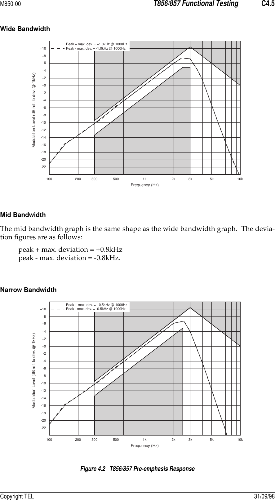
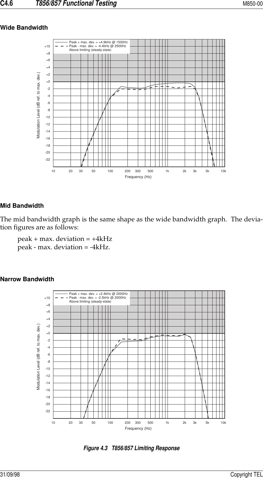
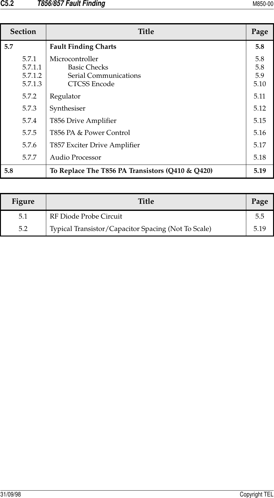
![M850-00T856/857 Functional TestingC4.1Copyright TEL 31/09/984 T856/857 Functional TestingCaution:This equipment contains CMOS devices which are susceptible to dam-age from static charges. Refer to Section 1.2 in Part A for more infor-mation on anti-static procedures when handling these devices.The following test procedures will confirm that the T856/857 has been tuned andadjusted correctly and is fully operational.Note 1:In this and following sections deviation settings are given first for widebandwidth sets, followed by settings in brackets for mid bandwidth sets ( )and narrow bandwidth sets [ ].Note 2:Unless otherwise specified, the term "PGM800Win" used in this and follow-ing sections refers to version 2.00 and later of the software.Refer to Figure 4.4 and Figure 4.5 for the location of the main tuning and adjustmentcontrols, and to Section 3.3 for the test equipment set-up. Refer also to Section 6 wherethe parts lists, grid reference index and diagrams will provide detailed information onidentifying and locating components and test points on the main PCB. The parts listand diagrams for the VCO PCB are in Part E.The following topics are covered in this section.Section Title Page4.1 Current Consumption 4.34.2 Output Power 4.34.3 Output Frequency 4.34.4 Timers 4.34.5 Frequency Response 4.44.6 Audio Level Input Sensitivity 4.7Figure Title Page4.14.24.34.44.5T856/857 Transmit TimersT856/857 Pre-emphasis ResponseT856/857 Limiting ResponseT856 Main Tuning & Adjustment ControlsT857 Main Tuning & Adjustment Controls4.44.54.64.94.11](https://usermanual.wiki/Tait/TEL0020/User-Guide-10227-Page-169.png)

![C4.4T856/857 Functional TestingM850-0031/09/98 Copyright TELFigure 4.1 T856/857 Transmit Timers4.5 Frequency ResponseIf the T856/857 has been correctly adjusted, the pre-emphasis and limiting responsesshould closely match those shown in Figure 4.2 and Figure 4.3 respectively. Note:The limits shown on these graphs should not be exceeded. • Measure the pre-emphasis response as follows: Reduce the line level to give ±1kHz (±0.8kHz) [±0.5kHz] deviation at 1kHz. Sweep the modulation frequency. The response should closely match that shown in Figure 4.2.• Measure the limiting response as follows: Set the line level to give ±3kHz (±2.4kHz) [±1.5kHz] deviation at 1kHz. Increase the line level 20dB and sweep the modulation frequency. The response should closely match that shown in Figure 4.3.Timer Function AdjustmentTransmit Tail Sets the tail time during which the transmitter stays keyed after the exter-nal key source has been removed.0-5 seconds in 100ms stepsTransmit Timeout Sets the maximum continuous trans-mission time. Once the timer has timed out, the transmitter must be keyed again, unless prevented by the transmit lockout timer.0-300 seconds in 10 second stepsTransmit Lockout Sets the period of time that must elapse after a timeout before the trans-mitter can re-transmit. Once the timer has timed out, the transmitter can be keyed again.0-60 seconds in 10 second stepsOnLockout TimeTimeoutTimeOnTail TimeTx-EnableTx-Reg.Tx-EnableTx-Reg.](https://usermanual.wiki/Tait/TEL0020/User-Guide-10227-Page-172.png)
![M850-00T856/857 Functional TestingC4.7Copyright TEL 31/09/984.6 Audio Level Input Sensitivity• Adjust RV210 (line sensitivity) fully clockwise.• Check that the input sensitivities are better than those specified below:Note:A degraded signal to noise ratio can be expected with the compressorselected. The extent of the degradation is dependent on the audio inputlevel.Line Input 600 ohms, ±3kHz (±2.4kHz) [±1.5kHz] deviation at 1kHz: with compressor -50dBm without compressor -30dBmMicrophone Input 600 ohms, ±3kHz (±2.4kHz) [±1.5kHz] deviation at 1kHz: with compressor -75dBm without compressor -55dBmCTCSS Input 1kHz deviation at 150Hz 500mV rms](https://usermanual.wiki/Tait/TEL0020/User-Guide-10227-Page-175.png)

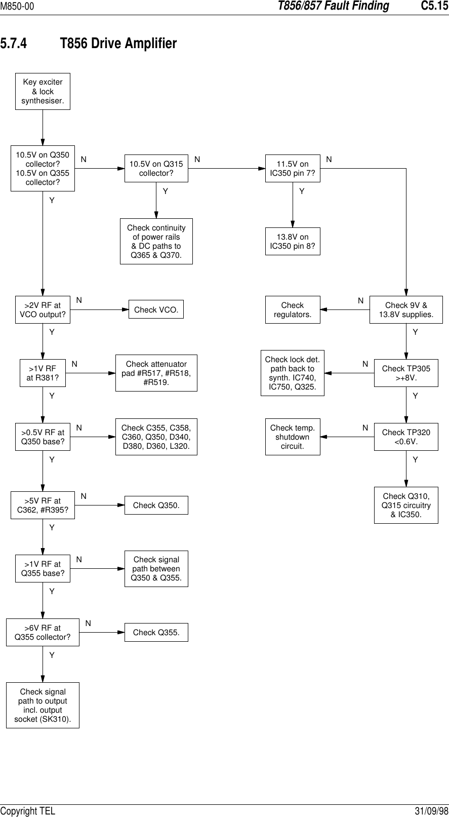
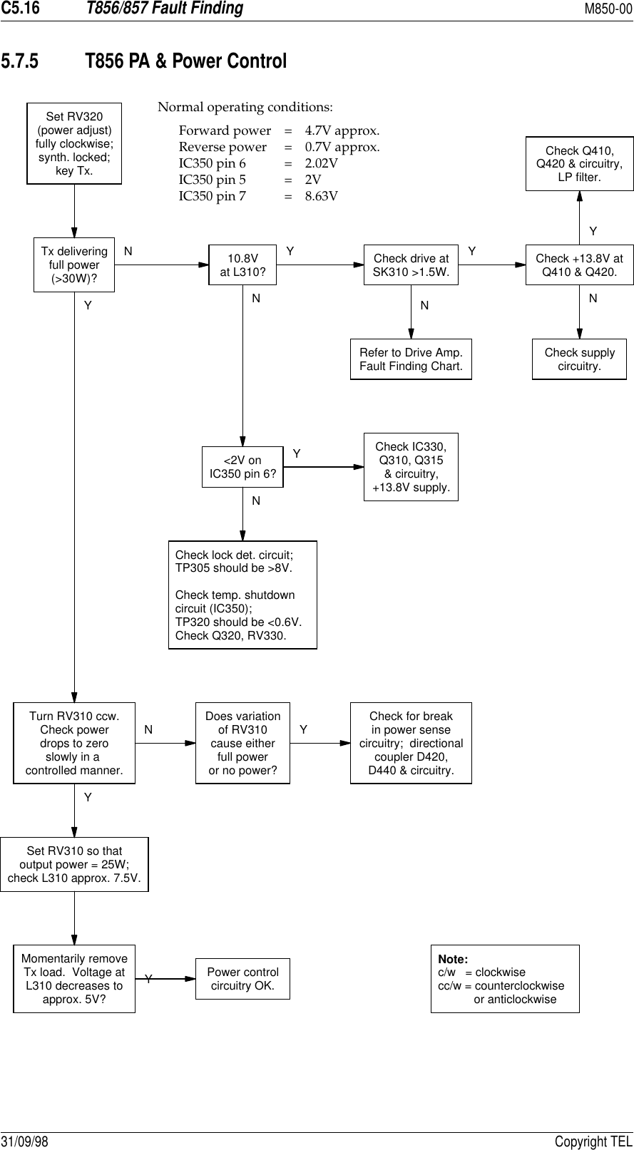
![M850-00T856/857 Fault FindingC5.1Copyright TEL 31/09/985 T856/857 Fault FindingCaution:This equipment contains CMOS devices which are susceptible to dam-age from static charges. Refer to Section 1.2 in Part A for more infor-mation on anti-static procedures when handling these devices.The following test procedures and fault finding flow charts may be used to help locate ahardware problem, however they are by no means a complete fault finding procedure.If you still cannot trace the fault after progressing through them in a logical manner,contact your nearest Tait Dealer or Customer Service Organisation. If necessary, you canget additional technical help from Customer Support, Radio Systems Division, Tait Elec-tronics Ltd, Christchurch, New Zealand (full contact details are on page 2).Note 1:In this and following sections deviation settings are given first for widebandwidth sets, followed by settings in brackets for mid bandwidth sets ( )and narrow bandwidth sets [ ].Note 2:Unless otherwise specified, the term "PGM800Win" used in this and follow-ing sections refers to version 2.00 and later of the software.Refer to Section 6 where the parts lists, grid reference index and diagrams will providedetailed information on identifying and locating components and test points on themain PCB. The parts list and diagrams for the VCO PCB are in Part E.The following topics are covered in this sectionSection Title Page5.1 Visual Checks 5.35.2 Component Checks 5.35.3 Front Panel LED Indicator 5.35.45.4.15.4.2DC ChecksPower RailsVCO Locking5.45.45.45.55.5.15.5.25.5.35.5.4RF ChecksT856 Drive PowerT856 PA Output PowerT857 Output PowerAudio And Modulation5.55.55.55.55.65.6 PGM800Win Generated Errors 5.7](https://usermanual.wiki/Tait/TEL0020/User-Guide-10227-Page-177.png)
![C5.6T856/857 Fault FindingM850-0031/09/98 Copyright TELConnect the exciter output to a power meter and key the exciter.Check that the output power is 1W ±300mW.Note:If the synthesiser is out of lock, the lock detector (synthesiser IC740 andcomparator IC750) will prevent the RF signal from reaching the PA byswitching the supply to the exciter amplifier (Q301, IC300, Q302, Q303).5.5.4 Audio And ModulationRefer to the audio processor fault finding chart (Section 5.7.7).Set up the audio processor as described in Section 3.9.Check that the demodulated RF output has the frequency response referred to inSection 4.5 with at least ±5kHz (±4kHz) [±2.5kHz] deviation available at 1kHzmodulating frequency.If the above result is not achieved, either the two modulators are incorrectly adjusted ora fault condition exists.](https://usermanual.wiki/Tait/TEL0020/User-Guide-10227-Page-182.png)


![G1.2T855 Link Selectable FeaturesM850-0031/09/98 Copyright TEL1.6 300Hz High Pass FilterLink PL240 also allows the insertion of this filter to improve hum and noise perform-ance.1.7 Audio Processor LinksThe tables in this section are the same as those in Section 3.5 in Part B. They have beenrepeated here for ease of reference.1.7.1 GeneralUse the following table to set up the audio processor to the configuration you require.You should set the audio processor links before carrying out the receiver alignment.The factory settings are shown in brackets [ ].Plug Linkaa. The letters in this column and in the table in Section 1.7.2 below refer to the identificationletters screen printed onto the PCB beside each set of pins.FunctionPL210 [1 - 2]2 - 3 [A - B]B - C de-emphasised responseflat responsePL220 1 - 2[2 - 3] D - E[E - F] flat responsede-emphasised responsePL230* 1 - 2[2 - 3]3 - 4M - N[N - P]P - Qaudio input via AUDIO-2 padaudio from internal CTCSS speech filteraudio input via I/O pad P250PL240bb. Refer to Section 1.7.2 for further details.1 - 2[2 - 3]or3 - 44 - 5G - H[H - J]orJ - KK - Lbypass high pass filter300Hz high pass filter in circuitaudio input via PL230 or I/O padPL250 [1 - 2]2 - 3 [R - S]S - T noise mutecarrier mutePL260 1 - 2[2 - 3] U - V[V - W] RX-DISABLE linknot connectedPL270 [1 - 2]2 - 3 [X - Y]Y - Z relay linknot connected](https://usermanual.wiki/Tait/TEL0020/User-Guide-10227-Page-326.png)
![M850-00T856/857 Optional FeaturesG2.1Copyright TEL 31/09/982 T856/857 Optional Features2.1 Audio ProcessorThe T856 and T857 come with a number of link selectable features which give addedsystem flexibility. Note:The tables in this section are the same as those in Section 3.5 in Part C. Theyhave been repeated here for ease of reference.2.1.1 Link DetailsUse the following table to set up the audio processor to the configuration you require.You should set the audio processor links before carrying out any of the tuning andadjustment procedures. The factory settings are shown in brackets [ ].Plug Linkaa. The letters in this column and in the table in Section 2.1.2 below refer to the identificationletters screen printed onto the PCB beside each pair of pins.FunctionPL2051-2[3-4]5-6ABCnot connectedmicrophone pre-amp. output to compressor inputmicrophone pre-amp. output to multiplexer inputPL210[1-2]3-45-6LMNmultiplexer output to pre-emphasis inputmultiplexer output to limiter inputmultiplexer output to compressor inputPL2151-2[3-4]5-67-89-10GHIJKnot connectedcompressor output to multiplexer inputcompressor output to limiter inputcompressor output to pre-emphasis inputnot connectedPL2201-2[3-4]5-6DEFpre-emphasis output to multiplexer inputpre-emphasis output to limiter inputnot connected](https://usermanual.wiki/Tait/TEL0020/User-Guide-10227-Page-329.png)
![G2.2T856/857 Optional FeaturesM850-0031/09/98 Copyright TEL2.1.2 Typical Options2.2 Line Transformer Inputs And OutputsThe line transformer (T210) is designed to provide a balanced interface to 600 ohm lines.For normal operation the two centre connections (LINE I/P 2, LINE I/P 3) are shortedtogether, and the 600 ohm line is connected between LINE I/P 1 and LINE I/P 4.The secondary winding of the transformer is connected via 1k and 10Ω (R160) resistorsto pin 6 (AUDIO-2) of D-range 1 and may be used to monitor audio on the line. Pin 7 ofD-range 1 can be reconfigured as AUDIO-1 by removing R808 and R160, and placing%R150 (refer to Section 2 in Part I for more details).2.3 Opto KeyThe keying circuitry may be completely isolated from the rest of the system by means ofthe optocoupler (IC250) connected between pins 11 and 12 of the D-range connector. Aconstant current source (Q270) allows keying voltages between 6 and 50V.2.4 Relay DriverA dedicated transistor (Q250) is provided for the purpose of switching an external (e.g.coaxial) relay. The output is open collector and is activated by the Tx-Reg rail. This out-put is available on pin 9 of the T800-03-0000 auxiliary D-range connector (D-range 2).PL205 PL210 PL215 PL220microphone pre-amp. compressedand pre-emphasised;line input pre-emphasised(standard set-up)[3-4]B[1-2]L[3-4]H[3-4]Emicrophone pre-amp. compressedand pre-emphasised;line input unprocessed3-4B3-4M7-8J1-2Dline and microphone compressedand pre-emphasised5-6C5-6N7-8J3-4Emicrophone pre-amp. compressed;line and microphone flat response3-4B3-4M3-4H5-6F](https://usermanual.wiki/Tait/TEL0020/User-Guide-10227-Page-330.png)