Tait TEL0038 Base Station Transmitter User Manual Cct Description Parts List Manual
Tait Limited Base Station Transmitter Cct Description Parts List Manual
UserManual.wiki
>
Tait
>
TEL0038 User Manual
>
Cct Description Parts List / Manual
Contents
1.
Cct Description Parts List / Manual
2.
Manual
Cct Description Parts List / Manual
Navigation menu
Upload a User Manual
Namespaces
Wiki Guide
HTML
PDF
Info
Views
User Manual
Discussion / Help
Navigation


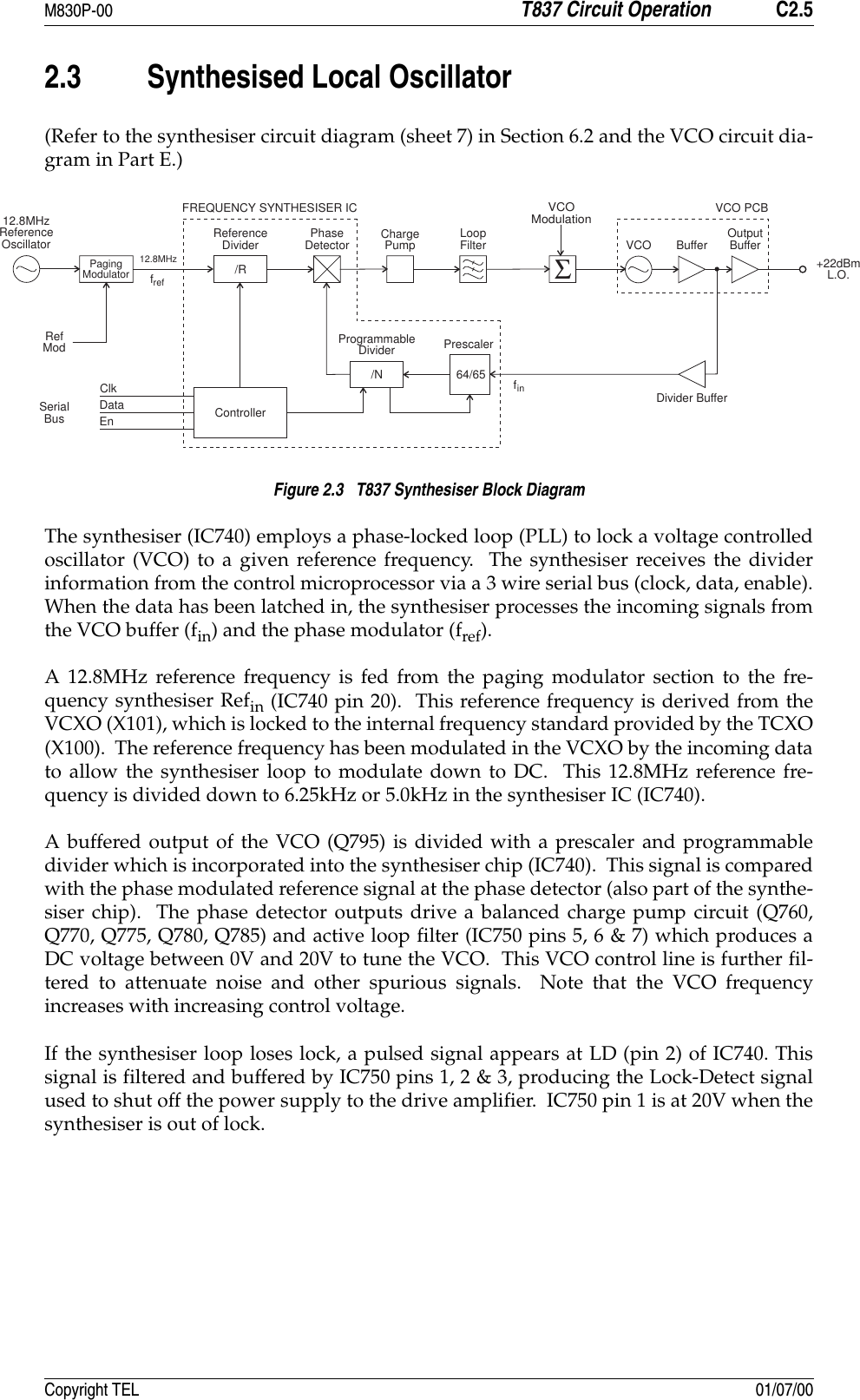
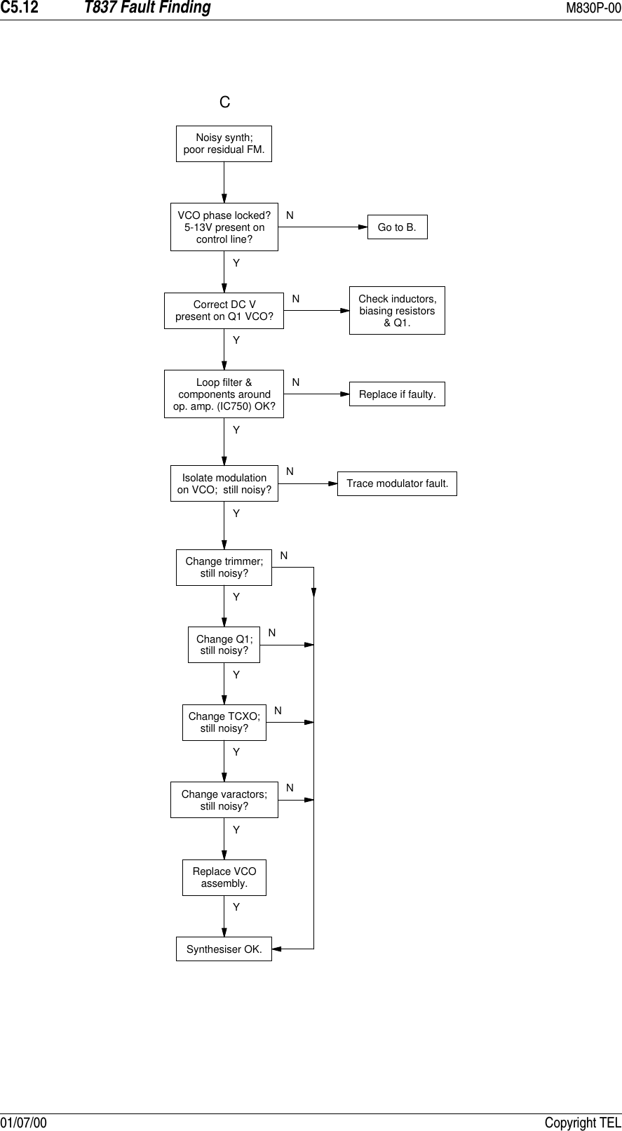
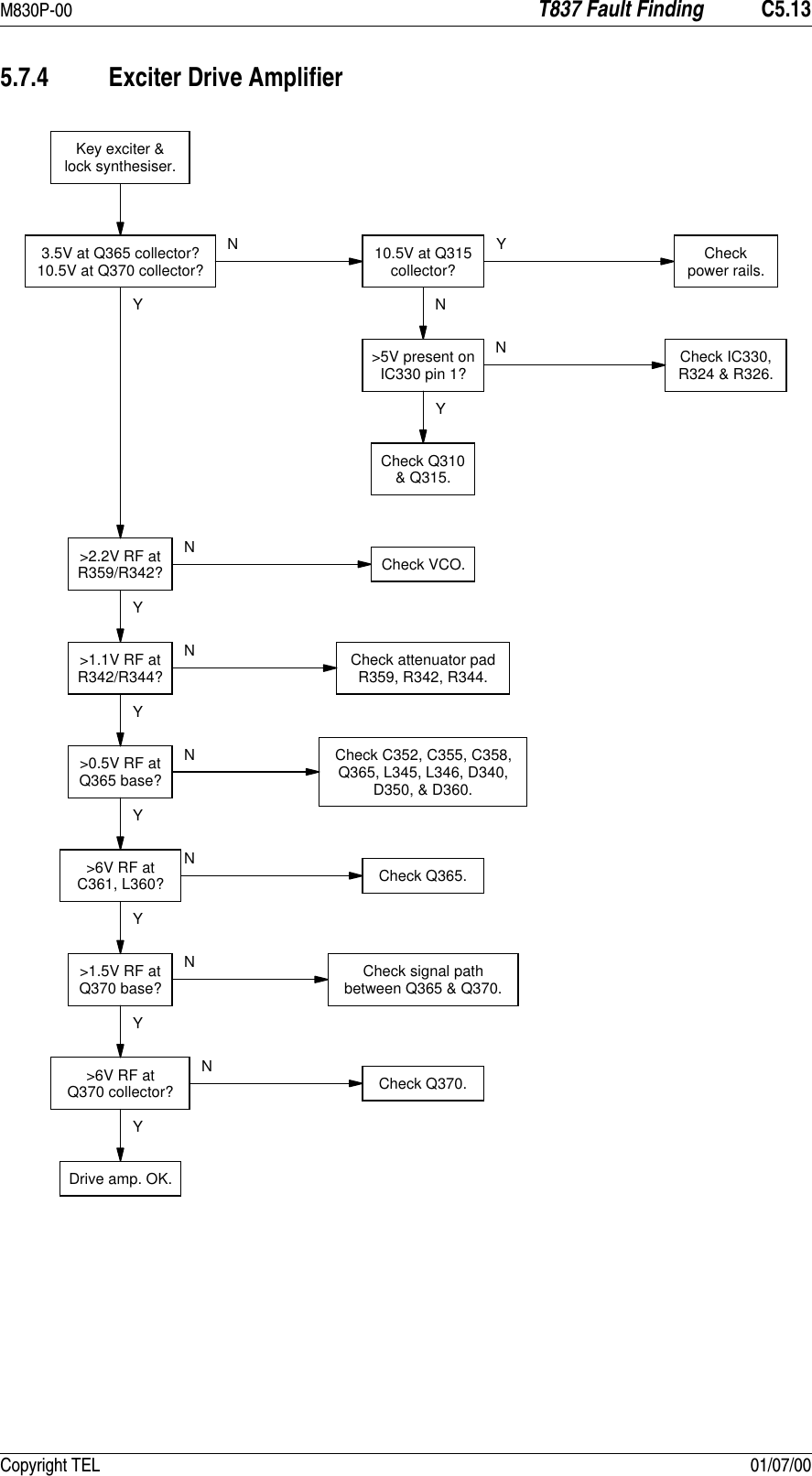
![C2.10 T837 Circuit Operation M830P-0001/07/00 Copyright TELWhen there is no external reference frequency present, *Q104 is turned off and *IC160switches 2.5V DC to the AFC input of the internal TCXO. The reference frequency canbe adjusted by the trimmer on the TCXO itself.When an external reference frequency is present, *Q104 switches on and *IC160 switchesthe synthesiser phase detector output voltage to the AFC input of the internal TCXO. Abuffered 12.8MHz output of the internal TCXO is fed back to the synthesiser oscillatorinput and compared with the external reference frequency, thus ensuring that the inter-nal TCXO is phase-locked to the external reference frequency.The synthesiser Lock-Detect signal drives an LED *D116 on the main PCB which is litwhen the synthesiser is locked to the external reference frequency. The Lock-Detect sig-nal is also fed to pin 8 of D-range 1 (PL100) for external monitoring purposes. The out-put is low when the synthesiser is locked.2.5.5 Keying InputsThere are two ways to key the exciter: • pulling the Tx-Key line low (pin 13 on D-range 1 [PL100]) at the rear of the set);• via the modem carrier detect line when the optional modem PCB is fitted.Note: Link S100 must be connected when using the Tx-Key line input.2.5.6 Paging Modulator LinksThree solder links are provided in the paging modulator circuit. Their functions aredescribed in the following table:Link FunctionStandardSetting DescriptionS100 Tx-Key linked ties the Tx-Key line to +5V for earthed Tx-Key line operationS101 invert data not linked inverts the incoming dataS102 invert key not linked inverts the key line (connected when using modem carrier detect)](https://usermanual.wiki/Tait/TEL0038.Cct-Description-Parts-List-Manual/User-Guide-117101-Page-42.png)


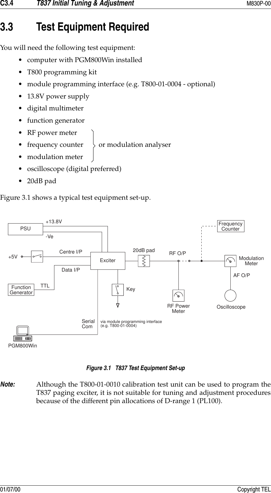


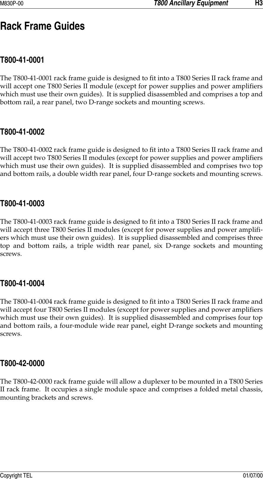
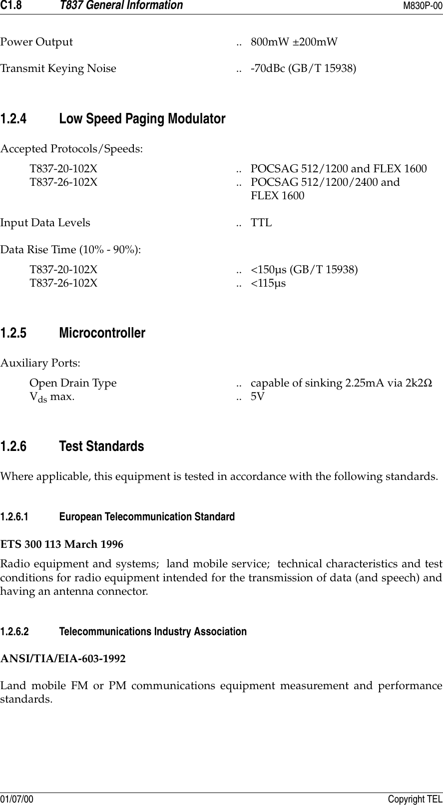
![M830P-00 T838/839 Initial Adjustment D3.3Copyright TEL 01/07/003.1 Test Equipment Required• DC power supply capable of delivering 30A at 13.8V.• Multimeter or DMM (e.g. Fluke 77).• RF power meter (e.g. HP 435 series or Bird Wattmeter). • 150W 30dB attenuator. • 150W 3dB 50 ohm pad. • 'BNC' to 'N' type adaptors (e.g. Amphenol, Greenpar). • Appropriate trimming tools. Figure 3.1 T838/839 Test Equipment Set-upCaution: Do not connect attenuators or DC blocks between the T837 and T838/839 or the cyclic keying circuitry will not function correctly.3.2 Preliminary ChecksCheck for short circuits between the positive rail and earth.Set up the test equipment as in Figure 3.1.Connect the T838/839 to a 13.8V DC supply.Check that the quiescent current is <50mA.To key the transmitter, earth the key line (D-range 1 [PL100] pin 13) on the exciter.Check that the power supply is still at 13.8V under load.Check that the regulated power control supply is approximately 7V.Note: The output power and alarm levels should be set with the side cover on. Ifthe cover is removed for other adjustment procedures, make a final check ofthe output power and alarm levels with the side cover on.Exciter PATx KeyRF PowerMeterTx Enable30dbAttenuator(HP 435)](https://usermanual.wiki/Tait/TEL0038.Cct-Description-Parts-List-Manual/User-Guide-117101-Page-113.png)