Tait TEL0040 Base Station Transmitter User Manual Cct Description Part List
Tait Limited Base Station Transmitter Cct Description Part List
Tait >
Cct Description Part List

M830P-00 1
Copyright TEL 01/07/00
T830 Series II Paging
Base Station Equipment
148-174MHz
Initial Adjustment Manual
July 2000
M830P-00-1A0

2M830P-00
01/07/00 Copyright TEL
Head Office
New Zealand
Tait Electronics Ltd
558 Wairakei Road
P.O. Box 1645
Christchurch
New Zealand
Phone: 64 3 358-3399
Fax: 64 3 358-3636
Radio Systems Division
535 Wairakei Road
P.O. Box 1645
Christchurch
New Zealand
Phone: 64 3 358-3399
Fax: 64 3 358-2825
Australia
Tait Electronics (Aust) Pty Ltd
186 Granite Street
Geebung
Queensland 4034
P. O . B o x 6 7 9
Virginia
Queensland 4014
Australia
Phone: 61 7 3865-7799
Toll Free: 1800 077-112
Fax: 61 7 3865-7990
Beijing
Tait Mobile Radio (HK) Ltd
Beijing Representative Office
Room 812, Tower A
Beijing Bright China
Chang An Building
No. 7 Jianguomennei Dai Jei
Dongcheng District
Beijing
China 100005
Canada
Tait Mobile Radio Inc.
Unit 5, 158 Anderson Avenue
Markham
Ontario L6E1A9
Canada
Phone: 1 905 472-1100
Toll Free: 1 800 890-8248
Fax: 1 905 472-5300
France
Tait France Sarl
2 Avenue de la Cristallerie
92 316 Sèvres, Cedex
France
Phone: 33 1 41 14-05-50
Fax: 33 1 41 14-05-55
Germany
Tait Mobilfunk GmbH
Willstätterstraße 50
D-90449 Nürnberg 60
Germany
Phone: 49 911 96 746-0
Fax: 49 911 96 746-79
Hong Kong
Tait Mobile Radio (HK) Ltd
Unit 2216, North Tower
Concordia Plaza
1, Science Museum Road
Tsim Sha Tsui East
Kowloon
Phone: 852 2369-3040
Fax: 852 2369-3009
New Zealand
Tait Communications Ltd
Unit 4, 75 Blenheim Road
P. O . B o x 11 8 5
Christchurch
Phone: 64 3 348-3301
Fax: 64 3 343-0558
Singapore
Tait Electronics (Far East) Pte
Ltd
4 Leng Kee Road
SIS Building #05-11A
Singapore 159088
Phone: 65 471-2688
Fax: 65 479-7778
Ta i w a n
Tait Mobile (Taiwan) Ltd
1104, No. 142 Chung Hsiao E. Rd
Sec. 4
Taipei
Taiwan
Phone: 886 2 2731-1290
Fax: 886 2 2711-6351
Thailand
Tait Mobile Radio Ltd
14/1 Suwan Tower
Third Floor
Soi Saladaeng 1
North Sathorn Road
Bangrak
Bangkok 10500
Thailand
Phone: 662 267-6290
Fax: 662 267-6293
United Kingdom
Tait Europe Ltd
Ermine Business Park
Ermine Road
Huntingdon
Cambridgeshire PE18 6YA
United Kingdom
Phone: 44 1480-52255
Fax: 44 1480-411996
USA
Tait Electronics (USA) Inc.
9434 Old Katy Road
Suite 110
Houston
Texas 77055
USA
Phone: 1 713 984-8684
Toll Free: 1 800 222-1255
Fax: 1 713 468-6944
Internet
http://www.taitworld.com
T800
T800

M830P-00 3
Copyright TEL 01/07/00
About This Manual
Scope This manual contains general, technical, tuning and adjustment
information on T830 Series II 50W and 100W paging base sta-
tions which comprise the following equipment:
PCB Information PCB information is provided for all current issue PCBs, as well
as all previous issue PCBs manufactured in production quanti-
ties, and is grouped according to PCB. Thus, you will find the
parts list, grid reference index (if necessary), PCB layouts and
circuit diagram(s) for each individual PCB grouped together.
Errors If you find an error in this manual, or have a suggestion on how
it might be improved, please do not hesitate to contact Customer
Support, Tait Electronics Ltd, Christchurch, New Zealand (full
contact details are on page 2).
Updating Equipment And Manuals
In the interests of improving performance, reliability or servicing, Tait Electronics Ltd
reserve the right to update their equipment and/or manuals without prior notice.
Copyright
All information contained in this manual is the property of Tait Electronics Ltd. All
rights are reserved. This manual may not, in whole or part, be copied, photocopied,
reproduced, translated stored or reduced to any electronic medium or machine readable
form without prior written permission from Tait Electronics Ltd.
Ordering Tait Service Manuals
You can order additional copies of this manual from your nearest Tait Dealer or Cus-
tomer Service Organisation. When ordering, make sure you quote the correct Tait prod-
uct code ("M" number). Note that only the latest issue of the manual will be available
for order.
50W base station T837 paging exciter
T838 50W power amplifier
100W base station T837 paging exciter
T839 100W power amplifier

4M830P-00
01/07/00 Copyright TEL
Table Of Contents
This manual is divided into eight parts as listed below, with each part being further sub-
divided into sections. There is a detailed table of contents at the start of each part and/
or section.
1
Part Title
A Introduction To Servicing
B T835 Receiver - not used in this manual
C T837 Paging Exciter
D T838 & T839 Power Amplifiers
E T830 VCO PCB Information
F Installation
G T800-28-0X00 Paging Rack Frame
H T800 Ancillary Equipment

M830P-00 AI
Copyright TEL 01/07/00
Part A Introduction To Servicing
This part of the manual is divided into the sections listed below. These sections provide
some general and advisory information on servicing procedures, and a brief history of
PGM800Win programming software.
Section Title Page
1
1.1
1.2
1.3
1.4
General
Additional Technical Information
Caution: CMOS Devices
Caution: Aerial Load
Caution: Beryllium Oxide & Power Transistors
1.1
1.1
1.1
1.2
1.2
2
2.1
2.2
2.3
2.3.1
2.3.2
2.4
2.5
Mechanical
Torx Recess Head Screws
Pozidriv & Philips Recess Head Screws
Disassembly/Reassembly
Exciters
Power Amplifiers
Cover Screw Torques
Chassis & Cover Compatibility
2.1
2.1
2.2
2.3
2.3
2.3
2.3
2.4
3
3.1
3.1.1
3.1.2
3.2
3.3
Component Replacement
Leaded Components
Desoldering Iron Method
Component Cutting Method
Surface Mount Devices
Cased Mica Capacitors
3.1
3.1
3.1
3.1
3.2
3.2
4
4.1
4.2
Software History
PGM800Win V1.0
PGM800Win V2.00
4.1
4.1
4.1
Figure Title Page
1.1
1.2
2.1
2.2
2.3
Typical Product Code & Serial Number Labels
Typical Anti-static Bench Set-up
Torx Screw Identification
Pozidriv & Philips Screw & Screwdriver Identification
Identification Of New-Design Chassis & Covers
1.1
1.2
2.1
2.2
2.4

AII M830P-00
01/07/00 Copyright TEL
M830P-00 General A1.1
Copyright TEL 01/07/00
1 General
1.1 Additional Technical Information
If you have any questions about this manual or the equipment it describes, please con-
tact your nearest Tait Dealer or Customer Service Organisation. If necessary, you can get
additional technical help from Customer Support, Tait Electronics Ltd, Christchurch,
New Zealand (full contact details are on page 2).
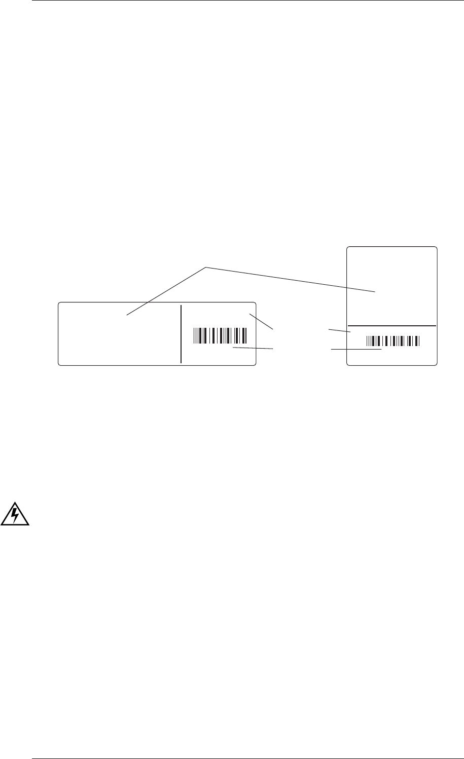
When requesting information, please quote either the manual product code (e.g.
M830P-00-1TA), or the equipment product code and serial number which are printed on
a label on the back of the product (as shown in Figure 1.1).
Figure 1.1 Typical Product Code & Serial Number Labels
If you require information about a particular PCB, please quote the full PCB internal
part number (IPN) which is screen printed onto the top side of the board (refer to the
appropriate PCB Information section in this manual for more details).
1.2 Caution: CMOS Devices
This equipment contains CMOS Devices which are susceptible to damage from static
charges. Care when handling these devices is essential. For correct handling proce-
dures refer to the manufacturers' data books, e.g. Philips data books covering CMOS
devices, or Motorola CMOS data books, Section 5 'Handling', etc.
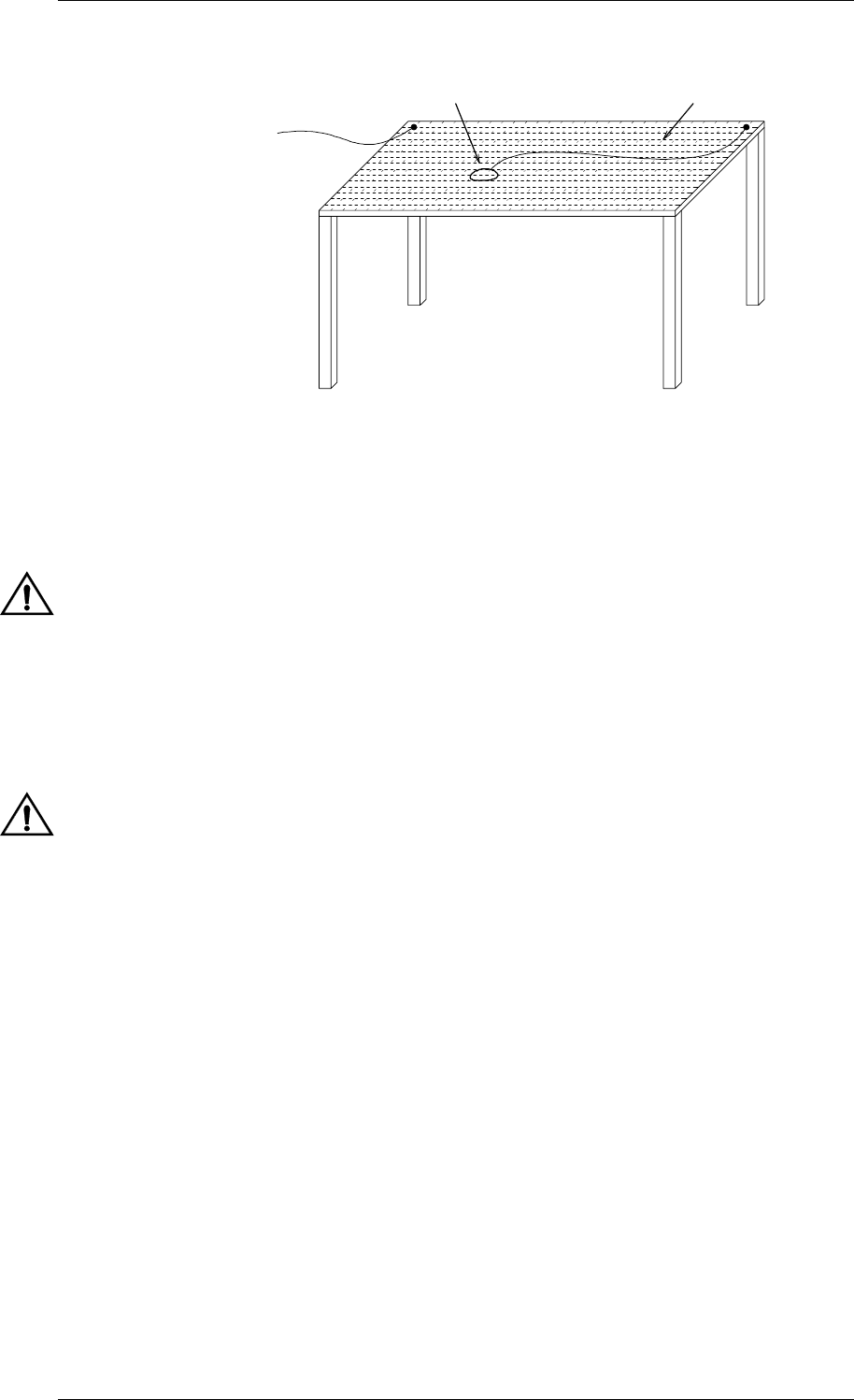
An anti-static bench kit (refer to Figure 1.2) is available from Tait Electronics Ltd under
the following product codes:
• KS0001 - 1 conductive rubber bench mat
- 1 earth lead to connect the mat to ground
• KS0004 - 1 wrist strap.
this area used for regional
Type Approval information
product code
serial number
T835-10-0000 Rev 1
900000
Tait Electronics Limited
Made in New Zealand
T838-10-0000
Rev 1
900000
Tait Electronics Limited
Made in New Zealand
A1.2 General M830P-00
01/07/00 Copyright TEL
Figure 1.2 Typical Anti-static Bench Set-up
1.3 Caution: Aerial Load
The equipment has been designed to operate safely under a wide range of aerial loading
conditions. However, we strongly recommend that the transmitter should always be
operated with a suitable load to prevent damage to the transmitter output power stage.
1.4 Caution: Beryllium Oxide & Power Transistors
The RF power transistors in current use all contain some beryllium oxide. This sub-
stance, while perfectly harmless in its normal solid form, can become a severe health
hazard when it has been reduced to dust. For this reason the RF power transistors
should not be broken open, mutilated, filed, machined, or physically damaged in any
way that can produce dust particles.
to building earth
(not mains earth)
conductive
wrist strap conductive rubber
bench mat

M830P-00 Mechanical A2.1
Copyright TEL 01/07/00
2 Mechanical
2.1 Torx Recess Head Screws
Torx recess head screws are becoming the standard screw head type in all T800 Series II
equipment, with Pozidriv and Philips recess head screws being used in fewer applica-
tions.
The Torx recess head has the advantage of improved screwdriver tip location, reducing
the chances of screw head damage caused by the driver tip rotating within the recess. In
addition, using a ball-tip Torx screwdriver allows you to drive a Torx head screw with
the driver on a slight angle, which can be useful in situations where access is restricted.
It is important that you use the correct Torx screwdriver tip:
M3 screws - T10
M4 screws - T20.
Figure 2.1 below shows a typical Torx recess head screw (actual hardware may differ
slightly from this illustration due to variations in manufacturing techniques).
Figure 2.1 Torx Screw Identification
"star" shaped recess with
six internal notches
A2.2 Mechanical M830P-00
01/07/00 Copyright TEL
2.2 Pozidriv & Philips Recess Head Screws
Pozidriv and Philips recess head screws will continue to be used in T800 Series II equip-
ment in a few special applications. It is important that you use the correct type and size
screwdriver for each screw type to avoid damaging the screw head.
It is particularly important that you do not use Philips screwdrivers on Pozidriv screw
heads as the tapered driving flutes of the Philips screwdriver do not engage correctly
with the parallel-sided slots in the Pozidriv screw head. This can result in considerable
damage to the screw head if the screwdriver tip turns inside the recess.
Note: If you find you need excessive downwards pressure to keep the screwdriver
tip in the Pozidriv screw head, you are probably using the wrong type and/
or size screwdriver.
Figure 2.2 below shows the main differences between typical Pozidriv and Philips screw
heads and screwdriver tips (actual hardware may differ slightly from these illustrations
due to variations in manufacturing techniques).
Figure 2.2 Pozidriv & Philips Screw & Screwdriver Identification
driving flutes with
parallel sides
driving flutes with
tapered sides
Pozidriv Philips
internal notches
"star" markings
between slots
no special markings
slots with parallel sides
slots with tapered sides
ridges between
driving flutes

M830P-00 Mechanical A2.3
Copyright TEL 01/07/00
2.3 Disassembly/Reassembly
2.3.1 Exciters
To carry out alignment or change option links, you need to remove only the top cover,
i.e. the one adjacent to the front panel handle and on the opposite side to the main
D-range connector (D-range 1/PL100).
You need to remove the bottom cover to access:
•Q370
• solder link SL501 (fast key option).
2.3.2 Power Amplifiers
You should carry out the tuning and power output level setting procedures with the
cover on.
2.4 Cover Screw Torques
Exciters .. 1.36Nm/12in.lbf.
Power Amplifiers .. 0.9Nm/in.lbf.
A2.4 Mechanical M830P-00
01/07/00 Copyright TEL
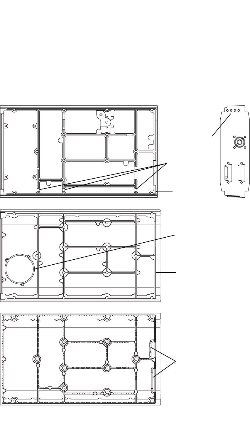
2.5 Chassis & Cover Compatibility
The chassis and covers used in T800 Series II modules incorporate a number of design
changes to improve Electro-Magnetic Compatibility (EMC) performance. It is impor-
tant that only the new-design covers are fitted to the new chassis to ensure correct
mechanical fit and continued compliance with appropriate EMC Type Approval regula-
tions.
Figure 2.3 below shows some of the main features which can be used to identify the
new-design chassis and covers.
Figure 2.3 Identification Of New-Design Chassis & Covers
Top Cover
Bottom Cover
Chassis
4 holes in
rear panel
loom channel in
top of walls
groove in top
of rear wall
ridge on top
of rear wall
provision for mounting speaker
(future development)
additional walls
←To p V iew Rear View→

M830P-00 Component Replacement A3.1
Copyright TEL 01/07/00
3 Component Replacement
3.1 Leaded Components
Whenever you are doing any work on the PCB that involves removing or fitting compo-
nents, you must take care not to damage the copper tracks. The two satisfactory meth-
ods of removing components from plated-through hole (PTH) PCBs are detailed below.
Note: The first method requires the use of a desoldering station, e.g. Philips SBC
314 or Pace MBT-100E.
3.1.1 Desoldering Iron Method
Place the tip over the lead and, as the solder starts to melt, move the tip in a circu-
lar motion.
Start the suction and continue the movement until 3 or 4 circles have been com-
pleted.
Remove the tip while continuing suction to ensure that all solder is removed from
the joint, then stop the suction.
Before pulling the lead out, ensure it is not stuck to the plating.
If the lead is still not free, resolder the joint and try again.
Note: The desoldering iron does not usually have enough heat to desolder leads
from the ground plane. Additional heat may be applied by holding a sol-
dering iron on the tip of the desoldering iron (this may require some addi-
tional help).
3.1.2 Component Cutting Method
Cut the leads on the component side of the PCB.
Heat the solder joint sufficiently to allow easy removal of the lead by drawing it
out from the component side: do not use undue force.
Fill the hole with solder and then clear with solderwick.

A3.2 Component Replacement M830P-00
01/07/00 Copyright TEL
3.2 Surface Mount Devices
Caution: Surface mount devices (SMDs) require special storage, handling,
removal and replacement techniques. This equipment should be serv-
iced only by an approved Tait Dealer or Customer Service Organisa-
tion equipped with the necessary facilities. Repairs attempted with
incorrect equipment or by untrained personnel may result in perma-
nent damage. If in doubt, contact your nearest Tait Dealer or Customer
Service Organisation.
3.3 Cased Mica Capacitors
Cased mica capacitors can be removed by heating the top with a heavy-duty soldering
iron and gently lifting the capacitor off the PCB with a solder-resistant spike or equiva-
lent.

M830P-00 Software History A4.1
Copyright TEL 01/07/00
4 Software History
28/06/96 PGM800Win Version 1.0
18/08/97 PGM800Win Version 2.00
4.1 PGM800Win V1.0
PGM800Win V1.0 is different in concept from DOS versions of PGM800 in that it is Win-
dows1 based. It also includes many new and improved features over DOS versions of
PGM800.
The major changes are outlined below:
• The Windows environment makes data entry and editing significantly easier.
• PGM800Win includes several new radio models which are not programmable
with DOS versions of PGM800.
• Out of range frequencies will result in warning messages and will not be accepted
for entry into the standard library module. User defined modules can be created,
however, allowing variation from the standard library module.
• Channel numbers default to 0-127 to match the EPROM memory locations. How-
ever, the user can change this setting so that the channel numbers run from 1-128
to suit his/her particular needs.
Note: The data files produced by BASEPROG V1.0 and all DOS versions of
PGM800 are still compatible with PGM800Win V1.0.
4.2 PGM800Win V2.00
PGM800Win V2.00 is an upgraded and expanded version of PGM800Win V1.0. It has
been developed specifically for T800 Series II base stations, but retains the ability to pro-
gram Series I equipment.
The major changes are outlined below:
• PGM800Win V2.0 will program T800 Series II base station modules via serial com-
munications.
• Deviation and reference modulation settings are written automatically to the
radio.
1. Windows is a registered trademark of the Microsoft Corporation.

A4.2 Software History M830P-00
01/07/00 Copyright TEL
• Extra information that is not stored in the radio (but which is still relevant to the
radio) can be saved to a file on disk (e.g. note field, auxiliary pin names, etc.).
Note: The data files produced by BASEPROG V1.0, all DOS versions of PGM800,
and PGM800Win V1.0 are still compatible with PGM800Win V2.00.

M830P-00 BI
Copyright TEL 01/07/00
Part B T835 Receiver
The T835 receiver is not covered in this manual. Refer to M830-00-201 (or later issue) for
servicing information on the T835.

BII M830P-00
01/07/00 Copyright TEL

M830P-00 CI
Copyright TEL 01/07/00
Part C T837 Paging Exciter
This part of the manual is divided into six sections, as listed below. There is a detailed
table of contents at the start of each section.
Section Title
1 General Information
2 Circuit Operation
3 Initial Tuning & Adjustment
4 Functional Testing
5 Fault Finding
6 PCB Information

CII M830P-00
01/07/00 Copyright TEL

M830P-00 T837 General Information C1.1
Copyright TEL 01/07/00
1 T837 General Information
This section provides a brief description of the T837 paging exciter, along with detailed
specifications and a list of types available.
The following topics are covered in this section.
Section Title Page
1.1 Introduction 1.5
1.2
1.2.1
1.2.2
1.2.3
1.2.4
1.2.5
1.2.6
1.2.6.1
1.2.6.2
1.2.6.3
Specifications
Introduction
General
RF Section
Low Speed Paging Modulator
Microcontroller
Test Sta nda rd s
European Telecommunication Standard
Telecommunications Industry Association
Chinese Radio Regulatory Commission
1.6
1.6
1.6
1.7
1.8
1.8
1.8
1.8
1.8
1.9
1.3 Product Codes 1.10
1.5 T837 Paging Product Range 1.11
Figure Title Page
1.1 T837 Main Circuit Block Identification 1.4
1.2 T837 Front Panel Controls 1.4

C1.2 T837 General Information M830P-00
01/07/00 Copyright TEL

M830P-00 T837 General Information C1.3
Copyright TEL 01/07/00
replace A4 pages C1.3/C1.4 with A3 pages C1.3/C1.4

C1.4 T837 General Information M830P-00
01/07/00 Copyright TEL
replace A4 pages C1.3/C1.4 with A3 pages C1.3/C1.4

M830P-00 T837 General Information C1.5
Copyright TEL 01/07/00
1.1 Introduction
The T837 is a synthesised, microprocessor controlled, DFSK low speed paging exciter
designed for single or multichannel1 operation in the 148 to 174MHz frequency range2.
With a standard power output of only 800mW, the exciter is designed for use with the
T839 100W power amplifier. The RF section of the exciter comprises a frequency syn-
thesiser which provides 170mW of frequency modulated RF drive to a two stage, wide
band output amplifier. The synthesiser frequency is programmed via the serial commu-
nications port.
The low speed paging modulator section provides DFSK modulation. It incorporates a
TCXO frequency reference and uses two point modulation to achieve modulation of
data rates from 2400bps down to DC.
All components except those of the VCO are mounted on a single PCB. This is secured
to a die-cast chassis which is divided into compartments to individually shield each sec-
tion of circuitry. Access to both sides of the main circuit board is obtained by removing
each of the chassis lids. There is provision within the chassis to mount small option
PCBs.
The front panel has two indicator LEDs to show when the transmit carrier is on (red)
and when the DC supply is connected (green). The T837 is 60mm wide and occupies a
single space in a Tait rack frame, which has the ability to accommodate up to seven
standard modules.
1. Although you can program the microcontroller with up to 128 channels, you must
carry out the modulation adjustment procedure if you change frequency (see Section
3.5).
2. Although capable of operating over the 148-174MHz frequency range, the T837 has an
8MHz VCO switching range (see Section 1.2.3 and Section 3.1).

C1.6 T837 General Information M830P-00
01/07/00 Copyright TEL
1.2 Specifications
1.2.1 Introduction
The performance figures given are minimum figures, unless otherwise indicated, for
equipment tuned with the maximum switching range and operating at standard room
temperature (+22°C to +28°C) and standard test voltage (13.8V DC).
Where applicable, the test methods used to obtain the following performance figures are
those described in the EIA and ETS specifications. However, there are several parame-
ters for which performance according to the Chinese specification GB/T 15938 is given.
Refer to Section 1.2.6 for details of test standards.
Details of test methods and the conditions which apply for Type Approval testing in all
countries can be obtained from Tait Electronics Ltd.
1.2.2 General
Number Of Channels .. 128 (standard)1
Supply Voltage:
Operating Voltage .. 10.8 to 16V DC
Standard Test Voltage .. 13.8V DC
Polarity .. negative earth only
Polarity Protection .. crowbar diode
Line Keying Supply (if required) .. -50V DC
Supply Current:
Tran sm it .. <650 mA
Standby - T837-2X-1020 .. <150mA
- T837-2X-1021 .. <200mA
Operating Temperature Range .. -30°C to +60°C
Dimensions:
Height .. 183mm
Width .. 60mm
Length .. 320mm
Weight .. 2.1kg
Time-Out Timer (optional) .. 0 to 5 minutes2 adjustable in 10 sec-
ond steps
1. Additional channels may be factory programmed. Contact your nearest Tait Dealer or
Customer Service Organisation.
2. Adjustable from 0 to 10 minutes in PGM800Win version 2.12 and later.

M830P-00 T837 General Information C1.7
Copyright TEL 01/07/00
Tail Timer .. 0 to 5 seconds adjustable in 100ms1
steps
Tran sm it Ke y Time:
T837-20-102X .. <100ms
T837-26-102X .. <30ms
Transmit Lockout Timer .. 0 to 1 minute adjustable in 10 second
steps
1.2.3 RF Section
Frequency Range .. 148-174MHz
Modulation Type .. DFSK
Frequency Increment:
T837-20-102X .. 5 or 6.25kHz
T837-26-102X .. 2.5 or 3.125kHz
VCO Switching Range .. 8MHz
Load Impedance .. 50 ohms
Frequency Stability:
T837-2X-1020 .. ±1.0ppm, -20°C to +70°C
±2.0ppm, -30°C to +70°C
T837-2X-1021 .. ±1.5ppm, -30°C to +70°C
External Reference Frequency .. 100kHz to 25.6MHz in 100kHz steps
(T837-2X-1021)
External Reference Amplitude .. 0 to +10dBm into 50Ω
Adjacent Channel Power .. -75dBc (ETS)
(4.5kHz deviation) -70dBc (GB/T 15938)
Transmitter Side Band Noise:
(no modulation, 15kHz bandwidth)
At ±25kHz .. -95dBc
At ±1MHz .. -105dBc
Radiated Spurious Emissions:
Transmit .. -36dBm to 1GHz
-30dBm to 4GHz
Standby .. -57dBm to 1GHz
-47dBm to 4GHz
1. Adjustable in 20ms steps in PGM800Win version 2.12 and later.

C1.8 T837 General Information M830P-00
01/07/00 Copyright TEL
Power Output .. 800mW ±200mW
Transmit Keying Noise .. -70dBc (GB/T 15938)
1.2.4 Low Speed Paging Modulator
Accepted Protocols/Speeds:
T837-20-102X .. POCSAG 512/1200 and FLEX 1600
T837-26-102X .. POCSAG 512/1200/2400 and
FLEX 1600
Input Data Levels .. TTL
Data Rise Time (10% - 90%):
T837-20-102X .. <150µs (GB/T 15938)
T837-26-102X .. <115µs
1.2.5 Microcontroller
Auxiliary Ports:
Open Drain Type .. capable of sinking 2.25mA via 2k2Ω
Vds max. .. 5V
1.2.6 Test Standards
Where applicable, this equipment is tested in accordance with the following standards.
1.2.6.1 European Telecommunication Standard
ETS 300 113 March 1996
Radio equipment and systems; land mobile service; technical characteristics and test
conditions for radio equipment intended for the transmission of data (and speech) and
having an antenna connector.
1.2.6.2 Telecommunications Industry Association
ANSI/TIA/EIA-603-1992
Land mobile FM or PM communications equipment measurement and performance
standards.

M830P-00 T837 General Information C1.9
Copyright TEL 01/07/00
1.2.6.3 Chinese Radio Regulatory Commission
GB/T 15938 - 1995
General specification for equipment of radio paging systems.

C1.10 T837 General Information M830P-00
01/07/00 Copyright TEL
1.3 Product Codes
The three groups of digits in the T830 Series II product code provide information about
the model, type and options fitted, according to the conventions described below.
The following explanation of T830 Series II product codes is not intended to suggest that
any combination of features is necessarily available in any one product. Consult your
nearest Tait Dealer or Customer Service Organisation for more information regarding
the availability of specific models, types and options.
Model
The Model group indicates the basic function of the product, as follows:
T83X-XX-XXXX T837 exciter
T838 50W power amplifier
T839 100W power amplifier
Type
The Type group uses two digits to indicate the basic RF configuration of the product.
The first digit in the Type group designates the frequency range:
T83X-XX-XXXX ’2’ for 148-174MHz
The second digit in the Type group indicates the channel spacing:
T83X-XX-XXXX ’0’ for wide bandwidth (25kHz) - standard
’6’ for wide bandwidth (25kHz) - USA
Options
T83X-XX-XXXX The Options group uses four digits and/or letters to indicate
any options that may be fitted to the product. This includes
standard options and special options for specific customers.
’0000’ indicates a standard Tait product with no options fitted.
The large number of options precludes listing them here.

M830P-00 T837 General Information C1.11
Copyright TEL 01/07/00
1.4 T837 Paging Product Range
The following table lists the range of T837 paging product types available at the time
this manual was published. Consult your nearest Tait Dealer or Customer Service
Organisation for more information.
You can identify the exciter type by checking the product code printed on a label on the
rear of the chassis (Figure 1.1 in Part A shows typical labels). You can further verify the
exciter type by checking the placement of an SMD resistor in the table that is screen
printed onto the PCB (refer to Section 6.1 for more details).
Frequency Range (MHz) 148-174
Deviation (kHz) 5
Baud Rate (bps) 1200 1200 2400 2400
Frequency Increments (kHz) 5/6.25 5/6.25 2.5/3.125 2.5/3.125
TCXO
±1.0ppm -20°C to +70°C
±2.0ppm -30°C to +70°C ••
±1.5ppm -20°C to +70°C ••
Exciter Type: T837- 20-1020 20-1021 26-1020 26-1021

C1.12 T837 General Information M830P-00
01/07/00 Copyright TEL

M830P-00 T837 Circuit Operation C2.1
Copyright TEL 01/07/00
2 T837 Circuit Operation
This section provides a basic description of the circuit operation of the T837 paging
exciter.
Note: Unless otherwise specified, the term "PGM800Win" used in this and follow-
ing sections refers to version 2.00 and later of the software.
Refer to Section 6 where the parts lists, grid reference index and diagrams will provide
detailed information on identifying and locating components and test points on the
main PCB. The parts list and diagrams for the VCO PCB are in Part E.
The following topics are covered in this section.
Section Title Page
2.1 Introduction 2.3
2.2 Microcontroller 2.4
2.3
2.3.1
Synthesised Local Oscillator
Two Point Modulation
2.5
2.6
2.4
2.4.1
VCO
VCO Supply
2.7
2.7
2.5
2.5.1
2.5.2
2.5.3
2.5.4
2.5.5
2.5.6
Low Speed Paging Modulator
General
AFC/PLL Operation
Data Path
External Reference Frequency (T837-2X-1021 Only)
Keying Inputs
Paging Modulator Links
2.8
2.8
2.8
2.9
2.9
2.10
2.10
2.6 Power Supply & Regulator Circuits 2.11
2.7 Transmit Timers 2.12
2.8 Exciter Drive Amplifier 2.13

C2.2 T837 Circuit Operation M830P-00
01/07/00 Copyright TEL
Figure Title Page
2.1
2.2
2.3
2.4
2.5
2.6
T837 High Level Block Diagram
T837 Microcontroller Block Diagram
T837 Synthesiser Block Diagram
T837 AFC Block Diagram
T837 Power Supply & Regulators Block Diagram
T837 Transmit Timers
2.3
2.4
2.5
2.8
2.11
2.12
M830P-00 T837 Circuit Operation C2.3
Copyright TEL 01/07/00
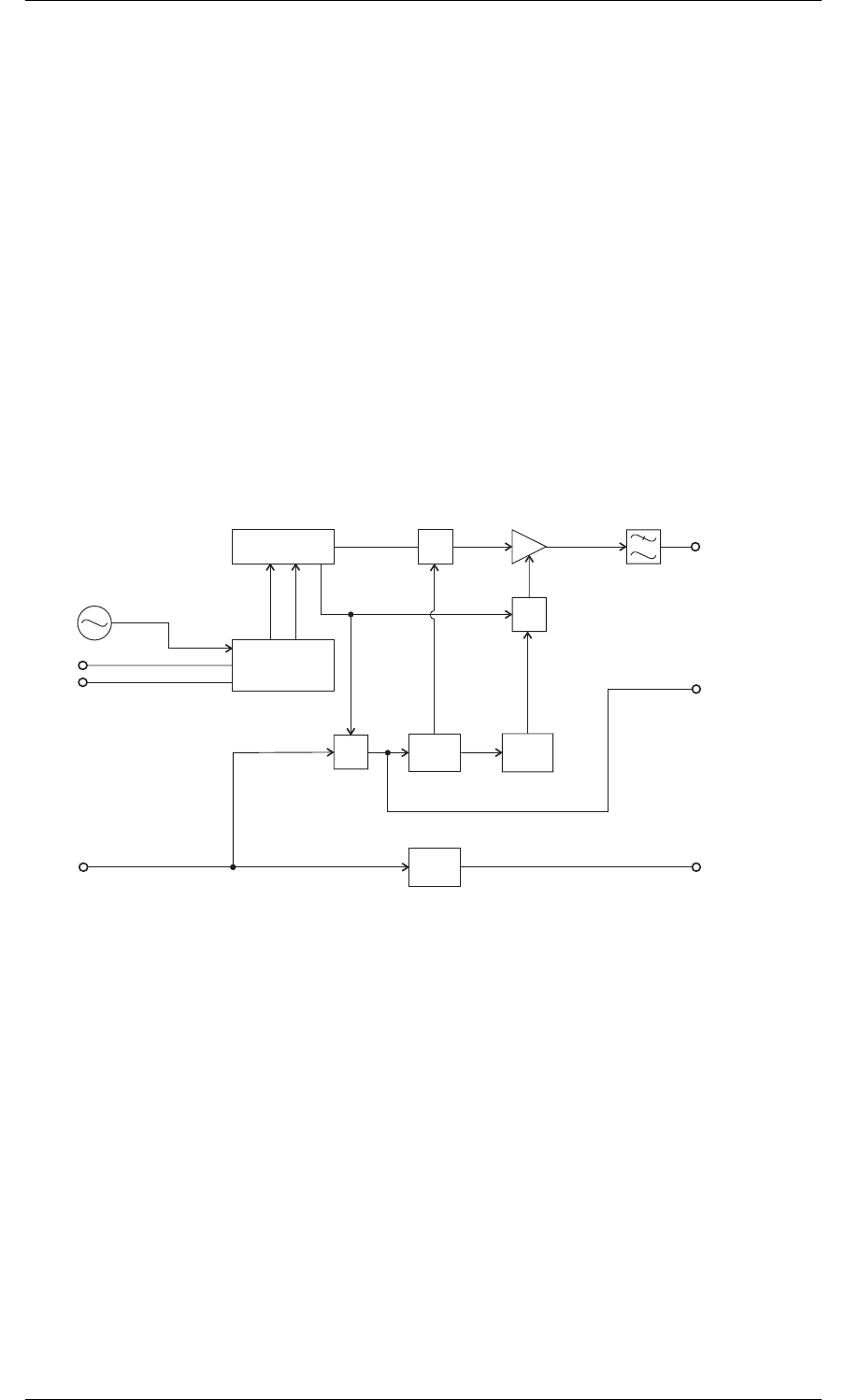
2.1 Introduction
The individual circuit blocks which make up the T837 are:
• synthesiser
•VCO
•paging modulator
•drive amplifier
• voltage regulators.
Each of these circuit blocks is set in its own shielded compartment, formed as an inte-
gral part of the main chassis.
The configuration of the circuit blocks may be seen on a functional level in Figure 2.1.
Refer to the circuit diagrams in Section 6.2 for more detail.
Figure 2.1 T837 High Level Block Diagram
Paging
Modulator
Synthesiser +22dBm
Reference
Oscillator
12.8MHz
Data
Lock
Detect
PIN
Switch
Switching
Control
Drive
Amp.
Gate
Exciter
Output
(800mW)
&Ramp
Gen.
Tx Reg VCO
Time
Delay
Time
Delay
Low Pass
Filter
PA Control Signal
(via exciter RF coax)

C2.4 T837 Circuit Operation M830P-00
01/07/00 Copyright TEL
2.2 Microcontroller
(Refer to the microcontroller circuit diagram (sheet 8) in Section 6.2.)
Figure 2.2 T837 Microcontroller Block Diagram
Overall system control of the T837 is accomplished by the use of a member of the 80C51
family of microcontrollers (IC810). It runs from internal ROM and RAM, thus leaving
all four ports free for input/output functions.
Non-volatile data storage is achieved by serial communication with a 16kBit EEPROM
(IC820). This serial bus is also used by the microcontroller to program the synthesiser
(IC740).
The main tasks of the microcontroller are as follows:
• program the synthesiser;
• interface with the PGM800Win programming software at 9600 baud via the
serial communication lines on D-range 1 (PL100);
• coordinate and implement timing control of the exciter;
• control the front panel "Supply" LED (refer to Section 5.3).
5V Reset
5V Digital
Regulator Watchdog
Reset
Channel
Select
Port
Auxiliary
Output
Port
Microcontroller
12.8MHz
Clock
Microcontroller Cavity
External
Serial
Port
EEPROM Synthesiser
Converter
M830P-00 T837 Circuit Operation C2.5
Copyright TEL 01/07/00
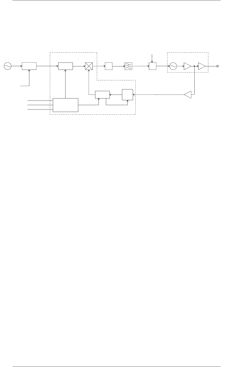
2.3 Synthesised Local Oscillator
(Refer to the synthesiser circuit diagram (sheet 7) in Section 6.2 and the VCO circuit dia-
gram in Part E.)
Figure 2.3 T837 Synthesiser Block Diagram
The synthesiser (IC740) employs a phase-locked loop (PLL) to lock a voltage controlled
oscillator (VCO) to a given reference frequency. The synthesiser receives the divider
information from the control microprocessor via a 3 wire serial bus (clock, data, enable).
When the data has been latched in, the synthesiser processes the incoming signals from
the VCO buffer (fin) and the phase modulator (fref).
A 12.8MHz reference frequency is fed from the paging modulator section to the fre-
quency synthesiser Refin (IC740 pin 20). This reference frequency is derived from the
VCXO (X101), which is locked to the internal frequency standard provided by the TCXO
(X100). The reference frequency has been modulated in the VCXO by the incoming data
to allow the synthesiser loop to modulate down to DC. This 12.8MHz reference fre-
quency is divided down to 6.25kHz or 5.0kHz in the synthesiser IC (IC740).
A buffered output of the VCO (Q795) is divided with a prescaler and programmable
divider which is incorporated into the synthesiser chip (IC740). This signal is compared
with the phase modulated reference signal at the phase detector (also part of the synthe-
siser chip). The phase detector outputs drive a balanced charge pump circuit (Q760,
Q770, Q775, Q780, Q785) and active loop filter (IC750 pins 5, 6 & 7) which produces a
DC voltage between 0V and 20V to tune the VCO. This VCO control line is further fil-
tered to attenuate noise and other spurious signals. Note that the VCO frequency
increases with increasing control voltage.
If the synthesiser loop loses lock, a pulsed signal appears at LD (pin 2) of IC740. This
signal is filtered and buffered by IC750 pins 1, 2 & 3, producing the Lock-Detect signal
used to shut off the power supply to the drive amplifier. IC750 pin 1 is at 20V when the
synthesiser is out of lock.
/R
Reference
Divider
12.8MHz
Reference
Oscillator
Ref
Mod
Paging
Modulator
Phase
Detector Charge
Pump Loop
Filter
FREQUENCY SYNTHESISER IC
Serial
Bus
Clk
Data
En Controller
/N
Programmable
Divider
64/65
Prescaler
VCO PCB
VCO
Modulation
VCO Buffer Output
Buffer
+22dB
m
L.O.
Divider Buffer
f
ref
f
in
Σ
12.8MHz

C2.6 T837 Circuit Operation M830P-00
01/07/00 Copyright TEL
2.3.1 Two Point Modulation
Frequency modulation occurs by modulating both the VCO input and the synthesiser
reference input. This process is called two point modulation and ensures a flat modula-
tion response from 0 to 2400bps.
The PLL has a fast response time, allowing a Tx key-up time of <30ms. Because of this
fast response time the PLL sees lower modulation frequencies superimposed on the
VCO as an error and corrects for it, resulting in no modulation on the carrier. At modu-
lation frequencies greater than 300Hz the loop cannot correct fast enough and modula-
tion is seen on the carrier.
To achieve low frequency modulation, the reference oscillator is also modulated so that
the phase detector of IC740 detects no frequency error under modulation. Thus, the
synthesiser loop will not attempt to correct for modulation and the data frequency
response of the transmitter remains unaffected.

M830P-00 T837 Circuit Operation C2.7
Copyright TEL 01/07/00
2.4 VCO
(Refer to the VCO circuit diagram in Part E.)
The VCO transistor (Q1) operates in a common source configuration, with an LC tank
circuit coupled between its gate and drain to provide the feedback necessary for oscilla-
tion. The VCO control voltage from the loop filter (IC750 pin 7) is applied to the vari-
caps (D1-D4) to facilitate tuning within an 8MHz band of frequencies. A trimcap (CV1)
is used for coarse tuning of the VCO. The output from the oscillator circuit drives a cas-
code amplifier stage (Q2, Q3) which supplies +10dBm (typically) to a further stage of
amplification, Q5. This is the final amplifier on the VCO PCB, and delivers +22dBm
(typically) to the exciter drive amplifier.
A low level "sniff" is taken from the output of Q3 and used to drive the divider buffer
(Q795) for the synthesiser (IC740).
The VCO operates at the actual output frequency of the exciter, i.e. there are no multi-
plier stages. The VCO is modulated by superimposing the data signal onto the control
voltage and by frequency modulating the reference signal.
2.4.1 VCO Supply
The VCO is supplied from two switched +9V supplies under the control of the Tx-Reg.
supply.
The VCO (Q1) and buffer amplifier (Q2 & Q3) are supplied from one +9V switched sup-
ply by Q540 via the capacitor multiplier (Q550, C550).
The output amplifier is supplied from the other +9V supply by Q520, Q530, and Q510.
A delay circuit holds the VCO on for a short time after the Tx-Reg. supply has been
switched off. This is to allow the RF power circuits (both exciter and PA) to ramp down
in the correct manner before the VCO is switched off.
C2.8 T837 Circuit Operation M830P-00
01/07/00 Copyright TEL
2.5 Low Speed Paging Modulator
(Refer to the low speed paging modulator circuit diagram (sheet 2) in Section 6.2.)
2.5.1 General
The T837-2X-102X is a dedicated paging exciter. The low speed paging modulator sec-
tion of the exciter accepts TTL data at the D-range input and modulates the synthesiser
using a two point modulation method that provides modulation of data input frequen-
cies of 2400bps down to DC (all 1’s or all 0’s).
The paging modulator section incorporates a TCXO frequency reference and a modulat-
able VCXO which is locked to the reference frequency from the TCXO.
The paging modulator also has provision for fitting an optional FFSK modem PCB.
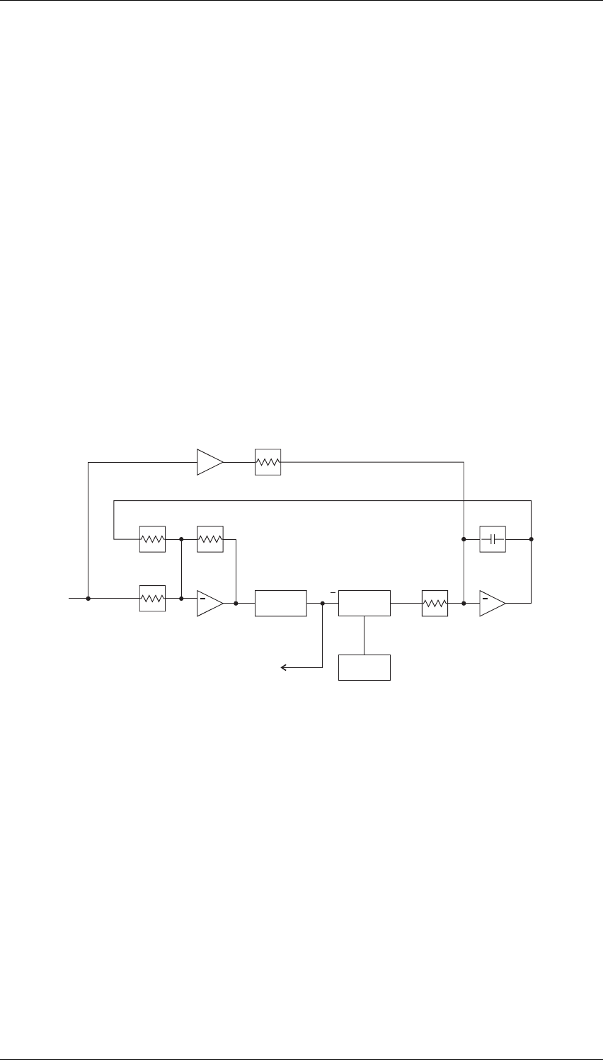
2.5.2 AFC/PLL Operation
Figure 2.4 T837 AFC Block Diagram
The TCXO is the default frequency standard. In PLL mode, the slave 12.8MHz VCXO is
phase locked to the TCXO. Both the TCXO and the VCXO outputs are clipped in IC100
and IC102 and then frequency divided by 4 in the twisted ring counters, IC105 (TCXO)
and IC110 (VCXO). The slave VCXO is also fed to the synthesiser reference input.
Each twisted ring counter provides four divide-by-four outputs, the Q and not Q having
the relative phases 0°, 90°, 180° and 270°. These two signals are combined in the two
XOR gate phase discriminators in IC115 to provide two beat frequencies that are in
phase quadrature. Both these outputs are filtered to pass the low frequency beat signal,
which is a 5Vpp triangle wave.
The output from pin 8 of IC115 is then differentiated to provide a further 90° phase
shifted square wave output on pin 14 of IC120. The amplitude of the output is propor-
tional to the frequency difference between the TXCO and the VCXO. The square wave
is then rectified by gating the signal with an inverted version of itself through a CMOS
VCXO AFC
12.8MHz
TCXO
Modulated
Reference
+
-1
Summing
Amp.
Loop Filter
Data Line

M830P-00 T837 Circuit Operation C2.9
Copyright TEL 01/07/00
switch. The switch is controlled by a square wave derived from the triangle wave on
pin 7 of IC120. This square wave will either be in-phase or inverted with respect to the
output on pin 14 of IC120, depending on whether the VCXO frequency is higher or
lower than the TCXO frequency.
The output from the CMOS switch (pin 14 of IC150) is a direct voltage which has ampli-
tude and sense that is relative to the beat frequency. This signal is used as the control
voltage for the VCXO. The rectified signal is then summed with an inverted version of
the data, which cancels the effect of the data on the loop filter but still allows the VCXO
to follow the TCXO frequency. Although the VCXO and TCXO are not on the same fre-
quency when data is being applied, the VCXO frequency will not drift with respect to
the TCXO.
2.5.3 Data Path
The input data enters the radio via pin 12 of D-range 1 (PL100). The data is fed into the
paging modulator at I/O pad P101, which is buffered by Q100, and then through an
XOR gate (IC115 pins 2 & 3) which gives the option of inverting the data.
IC140 pins 5 & 6 translate the level of the signal to 9Vpp, and then the data passes
through an attenuator and data filter. The data path is switched at the output of the fil-
ter by IC150 pins 1, 2 & 15, which allows the data to be removed from the AFC loop for
testing purposes.
From the switch the data travels three paths:
• The first path is via RV100 to the LOOP-MOD output to modulate the VCO.
• The second path is through RV101 to the summing amp. This data modulates
the control line of the VCXO, which produces the modulated reference.
• The third data path, which originates at the switch, is the feedforward data
path. The data is inverted, attenuated by RV102 and then summed with the
output of the AFC. The effect of this data path is to stop the loop filter from
correcting the VCXO frequency deviation caused by the data on the data line.
2.5.4 External Reference Frequency (T837-2X-1021 Only)
The paging modulator section of the T837-2X-1021 exciter incorporates an additional
synthesiser (*IC200) which can be configured to provide a 12.8MHz reference frequency
from an external frequency standard. This external frequency can be from 100kHz up to
25.6MHz in 100kHz steps.
When using an external reference, you must set the onboard synthesiser’s reference fre-
quency according to the frequency of the external reference. This is achieved by placing
resistors *%R240 - *%R247 in a pattern corresponding to a binary number which repre-
sents the reference divider ratio (see Section 3.6).
The internal TCXO (%X100) is used as the standard reference frequency, but is phase-
locked to the external frequency when this is applied.

C2.10 T837 Circuit Operation M830P-00
01/07/00 Copyright TEL
When there is no external reference frequency present, *Q104 is turned off and *IC160
switches 2.5V DC to the AFC input of the internal TCXO. The reference frequency can
be adjusted by the trimmer on the TCXO itself.
When an external reference frequency is present, *Q104 switches on and *IC160 switches
the synthesiser phase detector output voltage to the AFC input of the internal TCXO. A
buffered 12.8MHz output of the internal TCXO is fed back to the synthesiser oscillator
input and compared with the external reference frequency, thus ensuring that the inter-
nal TCXO is phase-locked to the external reference frequency.
The synthesiser Lock-Detect signal drives an LED *D116 on the main PCB which is lit
when the synthesiser is locked to the external reference frequency. The Lock-Detect sig-
nal is also fed to pin 8 of D-range 1 (PL100) for external monitoring purposes. The out-
put is low when the synthesiser is locked.
2.5.5 Keying Inputs
There are two ways to key the exciter:
• pulling the Tx-Key line low (pin 13 on D-range 1 [PL100]) at the rear of the set);
• via the modem carrier detect line when the optional modem PCB is fitted.
Note: Link S100 must be connected when using the Tx-Key line input.
2.5.6 Paging Modulator Links
Three solder links are provided in the paging modulator circuit. Their functions are
described in the following table:
Link Function
Standard
Setting Description
S100 Tx-Key linked ties the Tx-Key line to +5V for earthed Tx-Key
line operation
S101 invert data not linked inverts the incoming data
S102 invert key not linked inverts the key line (connected when using
modem carrier detect)
M830P-00 T837 Circuit Operation C2.11
Copyright TEL 01/07/00
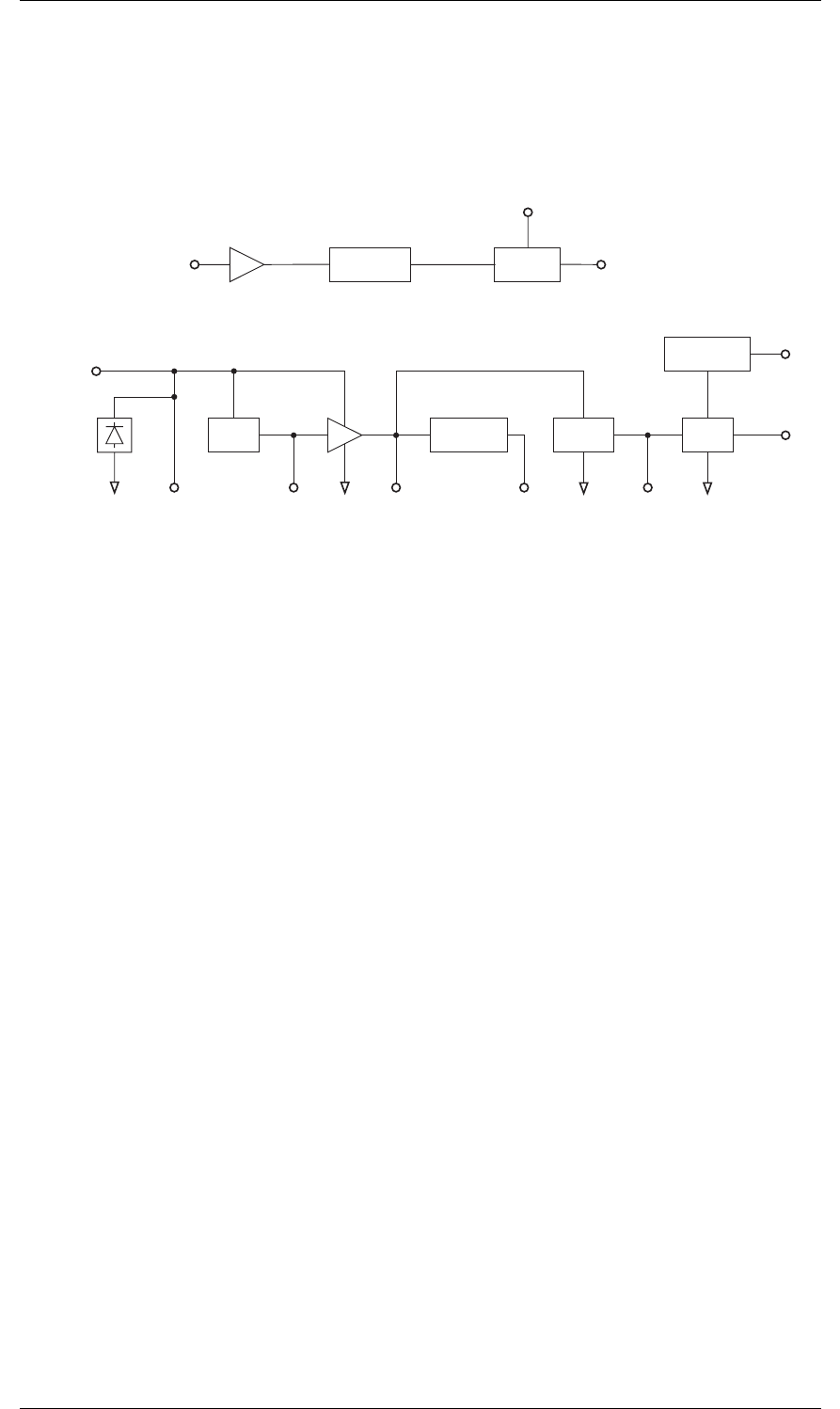
2.6 Power Supply & Regulator Circuits
(Refer to the regulators circuit diagram (sheet 6) in Section 6.2.)
Figure 2.5 T837 Power Supply & Regulators Block Diagram
The T837 is designed to operate from a 10.8-16V DC supply (13.8V nominal). A 5.3V
regulator (IC630) runs directly from the 13.8V rail, driving much of the synthesiser cir-
cuitry. It is also used as the reference for a DC amplifier (IC640, Q630, Q620) which pro-
vides a medium current capability 9V supply.
A switching power supply (Q660, Q670) runs from the 9V supply and provides a low
current capability +20V supply. This is used to drive the synthesiser loop filter (IC750),
giving a VCO control voltage range of up to 20V, and the Lock-Detect amplifiers.
Ultimate control of the transmitter is via the Tx-Reg. supply, switched from 9V by Q610.
This is enabled via the Tx-Enable signal from the modulator, and microprocessor.
A crowbar diode is fitted for protection against connection to a power supply of incor-
rect polarity. It also provides transient overvoltage protection.
Note: A fuse must be fitted in the power supply line for the diode to provide effec-
tive protection.
Crowbar
Diode LVI
5V
Reg
DC
Amp Switching
PS 5V Dig
Reg
Power
Switch
13.8V
Nom. 5V 5V Dig9V 20V
13.8V Nom.
From Rear
D-Range
Tx Enable
Buffer
Tx Reg.
+9V
µP
Watchdog
Timer
Micro-
controller
µP
Reset
C2.12 T837 Circuit Operation M830P-00
01/07/00 Copyright TEL
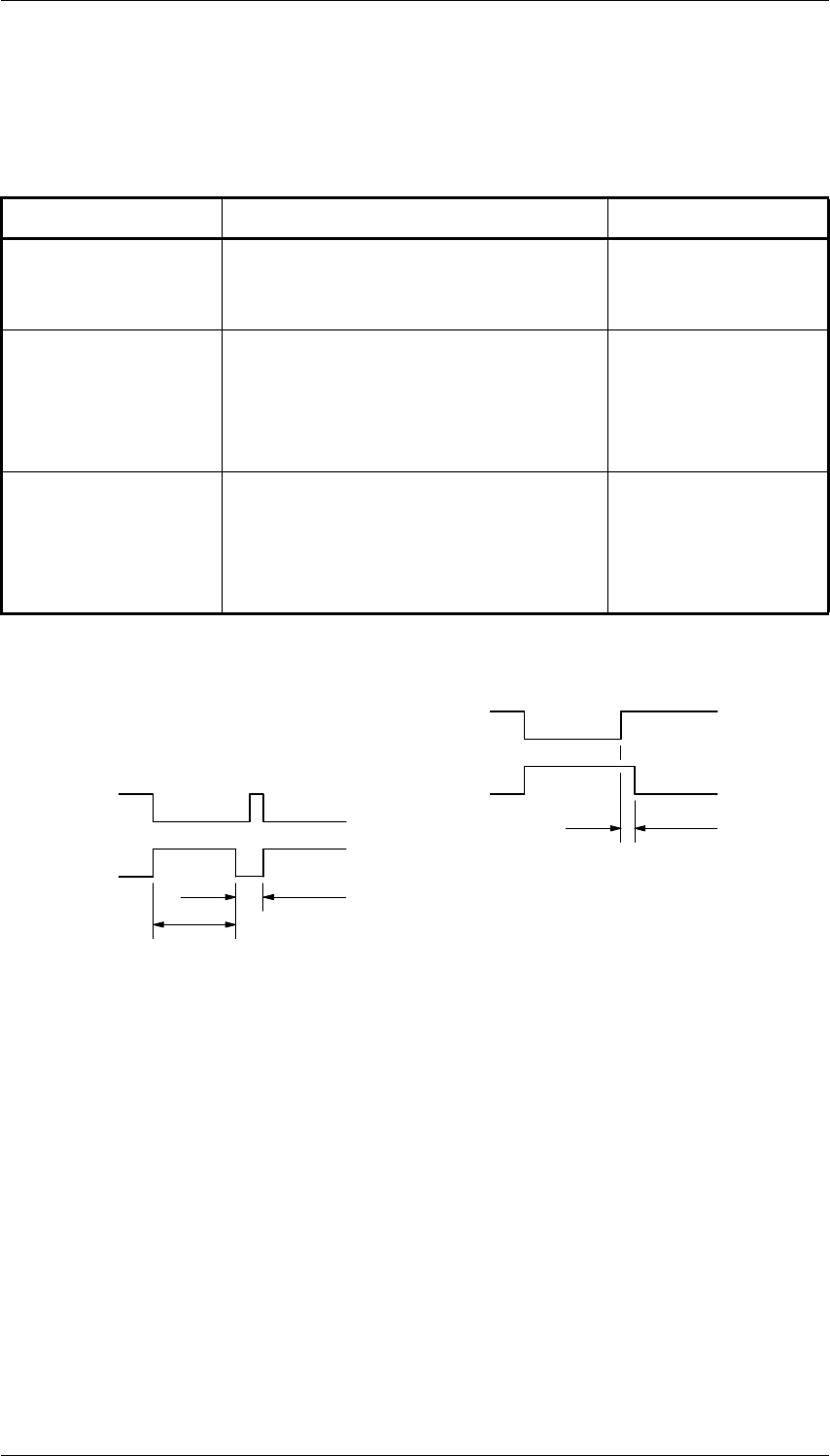
2.7 Transmit Timers
The transmit tail timer, transmit timeout timer and transmit lockout timer can all be set
from PGM800Win. The fields for setting these are found on the system information
page. These three timers operate as follows (refer also to Figure 2.6):
Figure 2.6 T837 Transmit Timers
Timer Function Adjustment
Transmit Tail Sets the tail time during which the
transmitter stays keyed after the exter-
nal key source has been removed.
0-5 seconds in 100ms
stepsa
a. Adjustable in 20ms steps in PGM800Win version 2.12 and later.
Transmit Timeout Sets the maximum continuous trans-
mission time. Once the timer has
timed out, the transmitter must be
keyed again, unless prevented by the
transmit lockout timer.
0-300 secondsb in 10
second steps
b. Adjustable from 0 to 600 seconds in PGM800Win version 2.12 and later.
Transmit Lockout Sets the period of time that must
elapse after a timeout before the trans-
mitter can re-transmit. Once the timer
has timed out, the transmitter can be
keyed again.
0-60 seconds in 10
second steps
On
Lockout Time
Timeout
Time
On
Tail Time
Tx-Enable
Tx-Reg.
Tx-Enable
Tx-Reg.

M830P-00 T837 Circuit Operation C2.13
Copyright TEL 01/07/00
2.8 Exciter Drive Amplifier
(Refer to Figure 2.1 and the exciter circuit diagram (sheet 3) in Section 6.2.)
A two-stage, wide band amplifier (Q365, Q370) provides an output level of approxi-
mately 800mW (+29dBm) for an input of 170mW (+22dBm) from the VCO. IC330 pins
5, 6 & 7, Q310, and Q315 provide a 10.5V regulated supply for the exciter.
To reduce the spurious output level when the synthesiser is out-of-lock, the Tx-Reg. and
Lock-Detect signals are gated to inhibit the exciter control circuit and to switch off the
RF signal at the input to the drive amplifier. This is achieved by a PIN switch attenuator
(D340, D350, D360).
Cyclic keying control is provided by additional circuitry consisting of several time
delay, ramp and gate stages:
• Q305, IC330 pins 5, 6 & 7 power ramping
• Q340, Q345 Tx-Reg. and Lock-Detect gate
• Q320, Q325, Q330, Q335 delay and PIN switch drive.
This is to allow the RF power circuits (both exciter and PA) to ramp up and down in a
controlled manner so that minimal adjacent channel interference is generated during
the transition.
R359, R342 and R344 form a 6dB attenuator to provide good VCO/drive amplifier isola-
tion.
The output attenuator (R360, R362, R364, R366) assists in reducing exciter/PA interac-
tion while also ensuring a good match for Q370.
Note: The exciter provides a DC control signal to the PA via the RF coax. This is
injected via L390.

C2.14 T837 Circuit Operation M830P-00
01/07/00 Copyright TEL

M830P-00 T837 Initial Tuning & Adjustment C3.1
Copyright TEL 01/07/00
3 T837 Initial Tuning & Adjustment
Caution: This equipment contains CMOS devices which are susceptible to dam-
age from static charges. Refer to Section 1.2 in Part A for more infor-
mation on anti-static procedures when handling these devices.
The following section describes the full tuning and adjustment procedure and provides
information on:
• channel programming
• synthesiser alignment
• modulator adjustment
• external reference frequency configuration (T837-2X-1021 only).
Note: Unless otherwise specified, the term "PGM800Win" used in this and follow-
ing sections refers to version 2.00 and later of the software.
Refer to Section 6 where the parts lists, grid reference index and diagrams will provide
detailed information on identifying and locating components and test points on the
main PCB. The parts list and diagrams for the VCO PCB are in Part E.
Section Title Page
3.1 Introduction 3.3
3.2 Channel Programming 3.3
3.3 Test Equipment Required 3.4
3.4 Synthesiser Alignment 3.5
3.5 Modulator Adjustment 3.6
3.6 External Reference Frequency Configuration
(T837-2X-1021 Only)
3.7
Figure Title Page
3.1
3.2
T837 Test Equipment Set-up
T837 100Hz VCO Control Line Wave Form
3.4
3.6

C3.2 T837 Initial Tuning & Adjustment M830P-00
01/07/00 Copyright TEL

M830P-00 T837 Initial Tuning & Adjustment C3.3
Copyright TEL 01/07/00
3.1 Introduction
When you receive your T837 exciter it will be run up and working on a particular fre-
quency (the "default channel")1. If you want to switch to a frequency that is within the
8MHz VCO switching range (i.e. ±4MHz from the factory programmed frequency), you
will need to:
• reprogram the exciter with the PGM800Win software (refer to the PGM800Win
programming kit and Section 3.2 below);
• carry out the modulator adjustment procedure described in Section 3.5.
However, if you want to switch to a frequency outside the 8MHz VCO switching range,
you will have to:
• reprogram the exciter with the PGM800Win software;
• carry out the synthesiser alignment procedure described in Section 3.4;
• carry out the modulator adjustment procedure described in Section 3.5.
3.2 Channel Programming
You can program up to 128 channel frequencies into the exciter’s EEPROM memory
(IC820) by using the PGM800Win software package and an IBM PC. You can also use
PGM800Win to select the exciter’s current operating frequency (or "default channel").
If the exciter is installed in a rack frame, you can program it via the programming port
in the speaker panel. However, you can also program the exciter before it is installed in
a rack frame as follows:
• by using a T800-01-0010 calibration test unit;
•via D-range 1.
If you do not use the T800-01-0010, you will have to connect the PC to the exciter via a
module programming interface (such as the T800-01-0004).
For a full description of the channel programming procedure, refer to the PGM800Win
programming software user’s manual.
1. Use the "Read Module" function in PGM800Win to find out what the default channel is.
C3.4 T837 Initial Tuning & Adjustment M830P-00
01/07/00 Copyright TEL
3.3 Test Equipment Required
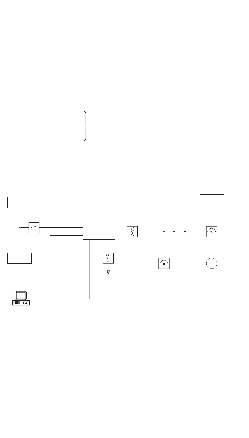
You will need the following test equipment:
• computer with PGM800Win installed
• T800 programming kit
• module programming interface (e.g. T800-01-0004 - optional)
• 13.8V power supply
• digital multimeter
• function generator
•RF power meter
•frequency counter
•modulation meter
• oscilloscope (digital preferred)
• 20dB pad
Figure 3.1 shows a typical test equipment set-up.
Figure 3.1 T837 Test Equipment Set-up
Note: Although the T800-01-0010 calibration test unit can be used to program the
T837 paging exciter, it is not suitable for tuning and adjustment procedures
because of the different pin allocations of D-range 1 (PL100).
or modulation analyser
P
G
M
800
Win
Serial
Com
PSU
+13.8V
-Ve
Frequency
Counter
RF Power
Meter Oscilloscope
AF O/P
Modulation
Meter
20dB pad
Function
Generator
Centre I/P
Data I/P
TTL Key
RF O/P
Exciter
via module programming interface
(e.g. T800-01-0004)
+5V

M830P-00 T837 Initial Tuning & Adjustment C3.5
Copyright TEL 01/07/00
3.4 Synthesiser Alignment
Ensure that the T837 has been programmed with the required frequencies using
PGM800Win software.
Select a channel using PGM800Win.
Connect a high impedance voltmeter to PL4-1 or the junction of L1 and R1 in the
VCO (this measures the synthesiser loop voltage).
Key the transmitter by earthing the Tx-Key line.
Tune VCO trimmer CV1 for a synthesiser loop voltage of 9V.
Check that the exciter output power is 800mW ±200mW (measured at the rear
panel N-type connector).
If required, measure and adjust the exciter output frequency as follows:
• apply +5V DC to pin 11 of D-range 1 (PL100) - this changes the mode of
operation to PLL so that the carrier frequency can be observed - and meas-
ure the output frequency at the rear panel N-type connector;
• adjust the trimmer on the TCXO (%X100) if required;
• remove the +5V DC from pin 11.
Caution: This trimmer is susceptible to physical damage. Do not exert a down-
ward force of more than 500g (1lb) when adjusting.

C3.6 T837 Initial Tuning & Adjustment M830P-00
01/07/00 Copyright TEL
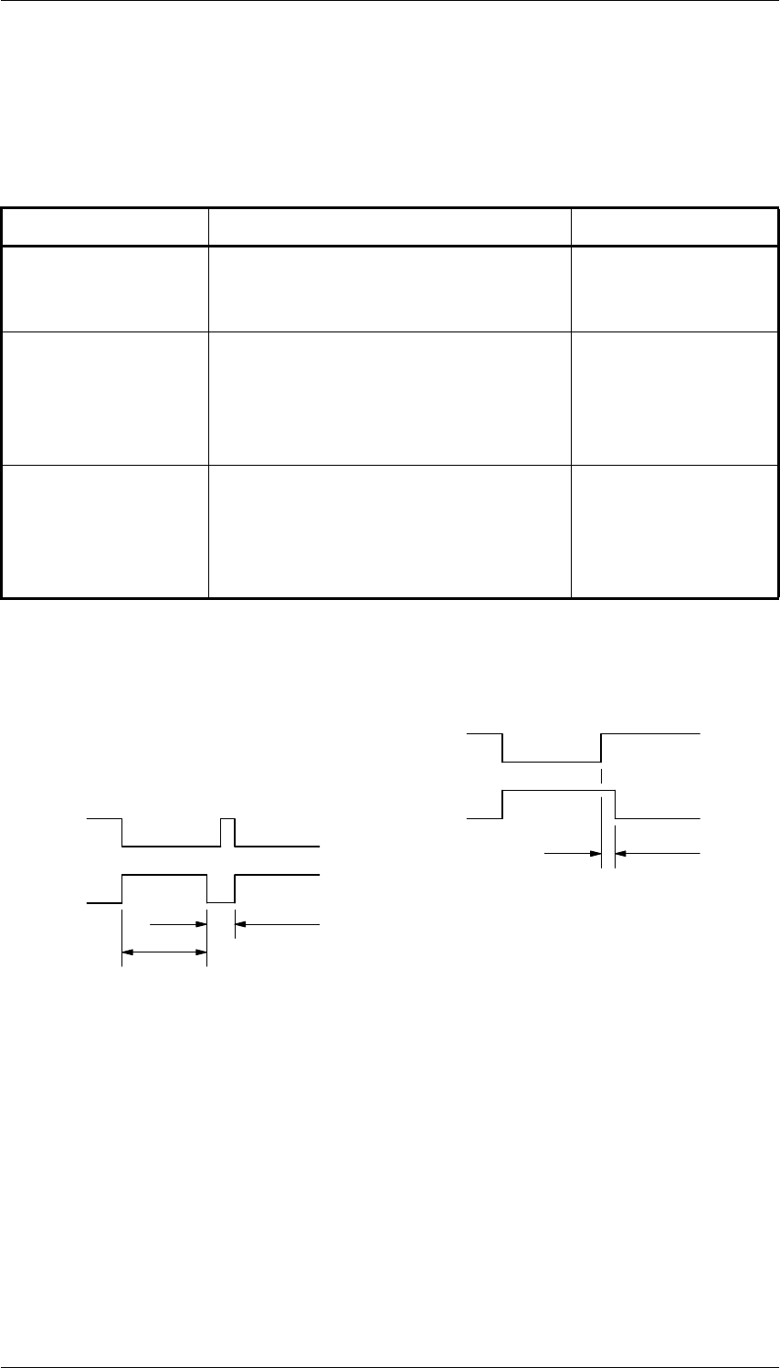
3.5 Modulator Adjustment
Apply +5V DC to pin 12 (DATA input) of D-range 1.
Monitor the exciter output frequency and adjust RV102 (DC frequency offset) to
give an output frequency of Fcarrier + 4.5kHz.
Remove the +5V DC from pin 12 and apply a 100Hz 5Vp-p square wave to pin 12.
Monitor the signal at TP100 with an AC coupled oscilloscope set to 50mV/div.
and adjust RV101 (reference modulation) until the triangle wave amplitude is
minimised.
Change the frequency of the square wave to 600Hz.
Monitor the frequency deviation on the exciter output with a modulation meter
and adjust RV100 (VCO modulation) to obtain ±4.5kHz deviation.
Monitor the VCO control line at PL4-1 or the junction of L1 and R1 in the VCO
using an AC coupled oscilloscope set to at least 20mV/div.
Change the frequency of the square wave back to 100Hz and check that the control
line still has a good trapezoidal wave form with flat top and bottom.
Note 1: You may have to readjust RV101 & RV100 alternately to achieve a square
wave on the VCO control line at both 600Hz and 100Hz with a deviation of
±4.5kHz. Figure 3.2 shows a typical 100Hz VCO control line wave form
with RV101 and RV100 set correctly.
Figure 3.2 T837 100Hz VCO Control Line Wave Form
Note 2: If the lower cut off frequency of an AC coupled oscilloscope is too high,
excessive distortion may be introduced which will result in ‘sag’ on the
square wave displayed. Determine if this is a problem by directly monitor-
ing the original square wave source and observe any sag. If there is sag,
switch the oscilloscope to DC and use a 10µF capacitor in series with the
oscilloscope probe (observing the correct polarity) to directly monitor the
VCO control line. Note that the trace settling time will be approximately
one minute.

M830P-00 T837 Initial Tuning & Adjustment C3.7
Copyright TEL 01/07/00
3.6 External Reference Frequency Configuration
(T837-2X-1021 Only)
When using an external reference frequency, you must set the onboard synthesiser’s ref-
erence frequency according to the frequency of the external reference. This is achieved
by placing resistors *%R240 - *%R247 in a pattern corresponding to a binary number
which represents the reference divider ratio.
If you are using a 10MHz external reference frequency, you need only carry out steps 4
and 5 in this section. You do not need to carry out steps 1, 2 and 3 because the T837 has
already been configured at the factory for a 10MHz external reference.
However, if you are using an external reference frequency other than 10MHz, you must
configure the internal synthesiser as described in steps 1, 2 and 3 before proceeding to
steps 4 and 5.
1. Divide the external oscillator frequency by 100kHz.
2. Convert the result to binary. You can use the following table to do this: select the
binary values in row three which add up to the result obtained in step 1, then
place a “1” in these positions and a “0” in the others.
3. Where there is a “0” in the binary number, place a zero ohm resistor in the corre-
sponding component location shown in the table. Where there is a “1”, leave an
open link.
Example: The following example shows the resistor pattern for a 10MHz external ref-
erence frequency is calculated.
10MHz
100kHz =100
100 = 64 + 32 + 4
therefore place resistors *%R240, *%R243, *%R244, *%R246
and *%R247 and leave all other links open
MSB LSB
N7 N6 N5 N4 N3 N2 N1 N0
12810 6410 3210 1610 810 410 210 110
*%R240 *%R241 *%R242 *%R243 *%R244 *%R245 *%R246 *%R247
MSB LSB
N7 N6 N5 N4 N3 N2 N1 N0
12810 6410 3210 1610 810 410 210 110
0 1 100100
*%R240 *%R241 *%R242 *%R243 *%R244 *%R245 *%R246 *%R247

C3.8 T837 Initial Tuning & Adjustment M830P-00
01/07/00 Copyright TEL
4. Connect the external reference frequency at a level of 0dBm to +10dBm/50Ω into
the external reference input and check that green LED *D116 lights.
5. Measure the TCXO (%X100) AFC voltage at %IC160 pin 4 with a high impedance
voltmeter and adjust the TXCO trimmer (if necessary) to obtain 2.5V DC ±0.2V.
M830P-00 T837 Functional Testing C4.1
Copyright TEL 01/07/00
4 T837 Functional Testing
Caution: This equipment contains CMOS devices which are susceptible to dam-
age from static charges. Refer to Section 1.2 in Part A for more infor-
mation on anti-static procedures when handling these devices.
The following test procedures will confirm that the T837 has been tuned and adjusted
correctly and is fully operational.
Note: Unless otherwise specified, the term "PGM800Win" used in this and follow-
ing sections refers to version 2.00 and later of the software.
Refer to Figure 4.2 for the location of the main tuning and adjustment controls, and to
Section 3.3 for the test equipment set-up. Refer also to Section 6 where the parts lists,
grid reference index and diagrams will provide detailed information on identifying and
locating components and test points on the main PCB. The parts list and diagrams for
the VCO PCB are in Part E.
The following topics are covered in this section.
Section Title Page
4.1 Current Consumption 4.3
4.2 Output Power 4.3
4.3 Output Frequency 4.3
4.4 External Reference Frequency (T837-2X-1021 Only) 4.3
4.5 Timers 4.4
Figure Title Page
4.1
4.2
T837 Transmit Timers
T837 Main Tuning & Adjustment Controls
4.4
4.5

C4.2 T837 Functional Testing M830P-00
01/07/00 Copyright TEL

M830P-00 T837 Functional Testing C4.3
Copyright TEL 01/07/00
4.1 Current Consumption
Connect the T837 to a 13.8V power supply.
Connect an RF power meter to the T837 output socket.
Check that the current in the 13.8V power cable is less than:
T837-2X-1020 - 150mA
T837-2X-1021 - 200mA.
Key the T837 by earthing the Tx-Key line (the carrier "On" LED should light).
Check that the current is less than 650mA.
4.2 Output Power
Connect an RF power meter to the T837 output socket.
Key the T837 by earthing the Tx-Key line.
Check that the output power is 800mW ±200mW.
4.3 Output Frequency
Connect the T837 output to a frequency counter via a 20dB attenuator pad.
Apply +5V DC to pin 11 of D-range 1 (PL100) - this changes the mode of operation
to PLL so that the carrier frequency can be observed - and measure the output fre-
quency.
Adjust the TCXO (X100) (if required) to trim to the nominal frequency (±100Hz).
4.4 External Reference Frequency (T837-2X-1021 Only)
Connect the external reference frequency at a level of 0dBm to +10dBm/50Ω into
the external reference input and check that green LED *D116 lights.
Note: Ensure that the onboard synthesiser’s reference frequency has been set
according to the frequency of the external reference (see Section 3.6).
Check the Lock-Detect signal level on pin 8 of D-range 1 (PL100) is as follows:
external reference frequency applied - 0V (approx.)
no external reference frequency applied - 4.5V (approx.).
C4.4 T837 Functional Testing M830P-00
01/07/00 Copyright TEL
4.5 Timers
The transmit tail timer, transmit timeout timer and transmit lockout timer can all be set
from PGM800Win. The fields for setting these are found on the system information
page. These three timers operate as follows (refer also to Figure 4.1):
Figure 4.1 T837 Transmit Timers
Timer Function Adjustment
Transmit Tail Sets the tail time during which the
transmitter stays keyed after the exter-
nal key source has been removed.
0-5 seconds in 100ms
stepsa
a. Adjustable in 20ms steps in PGM800Win version 2.12 and later.
Transmit Timeout Sets the maximum continuous trans-
mission time. Once the timer has
timed out, the transmitter must be
keyed again, unless prevented by the
transmit lockout timer.
0-300 secondsb in 10
second steps
b. Adjustable from 0 to 600 seconds in PGM800Win version 2.12 and later.
Transmit Lockout Sets the period of time that must
elapse after a timeout before the trans-
mitter can re-transmit. Once the timer
has timed out, the transmitter can be
keyed again.
0-60 seconds in 10
second steps
On
Lockout Time
Timeout
Time
On
Tail Time
Tx-Enable
Tx-Reg.
Tx-Enable
Tx-Reg.

M830P-00 T837 Fault Finding C5.1
Copyright TEL 01/07/00
5 T837 Fault Finding
Caution: This equipment contains CMOS devices which are susceptible to dam-
age from static charges. Refer to Section 1.2 in Part A for more infor-
mation on anti-static procedures when handling these devices.
The following test procedures and fault finding flow charts may be used to help locate a
hardware problem, however they are by no means a complete fault finding procedure.
If you still cannot trace the fault after progressing through them in a logical manner,
contact your nearest Tait Dealer or Customer Service Organisation. If necessary, you
can get additional technical help from Customer Support, Radio Systems Division, Tait
Electronics Ltd, Christchurch, New Zealand (full contact details are on page 2).
Note: Unless otherwise specified, the term "PGM800Win" used in this and follow-
ing sections refers to version 2.00 and later of the software.
Refer to Section 6 where the parts lists, grid reference index and diagrams will provide
detailed information on identifying and locating components and test points on the
main PCB. The parts list and diagrams for the VCO PCB are in Part E.
The following topics are covered in this section:
Section Title Page
5.1 Visual Checks 5.3
5.2 Component Checks 5.3
5.3 Front Panel LED Indicator 5.3
5.4
5.4.1
5.4.2
DC Checks
Power Rails
VCO Locking
5.4
5.4
5.4
5.5
5.5.1
RF Checks
Output Power
5.5
5.5
5.6 PGM800Win Generated Errors 5.6
5.7
5.7.1
5.7.1.1
5.7.1.2
5.7.2
5.7.3
5.7.4
Fault Finding Charts
Microcontroller
Basic Checks
Serial Communications
Regulator
Synthesiser
Exciter Drive Amplifier
5.7
5.7
5.7
5.8
5.9
5.10
5.13

C5.2 T837 Fault Finding M830P-00
01/07/00 Copyright TEL
Figure Title Page
5.1 RF Diode Probe Circuit 5.5

M830P-00 T837 Fault Finding C5.3
Copyright TEL 01/07/00
5.1 Visual Checks
Remove the covers from the T837 and inspect the PCB for damaged or broken compo-
nents, paying particular attention to the surface mounted devices (SMD's).
Check for defective solder joints. If repair or replacement is considered necessary, refer
to Section 3 of Part A.
5.2 Component Checks
If you suspect a transistor is faulty, you can assess its performance by measuring the for-
ward and reverse resistance of the junctions. Unless the device is completely desol-
dered, first make sure that the transistor is not shunted by some circuit resistance. Use a
good quality EVM (e.g. Fluke 75) for taking the measurements (or a 20k ohm/V or bet-
ter multimeter, using only the medium or low resistance ranges).
The collector current drawn by multi-junction transistors is a further guide to their per-
formance.
If an IC is suspect, the most reliable check is to measure the DC operating voltages. Due
to the catastrophic nature of most IC failures, the pin voltages will usually be markedly
different from the recommended values in the presence of a fault. The recommended
values can be obtained from either the circuit diagram or the component data catalogue.
5.3 Front Panel LED Indicator
The green "Supply" LED on the T837 front panel will flash according to the conditions
described in the following table:
Where two or more conditions occur at the same time, the precedence is in the order
shown above (i.e. T837 linked has the highest priority, followed by internal error).
Flash Rate Condition
fast (D sec. on/D sec. off
approx.) T837 is linked with PGM800Win
unequal (D sec. on/1 sec. off
approx.)
microcontroller has detected an
internal communications error -
refer to Section 5.7.1

C5.4 T837 Fault Finding M830P-00
01/07/00 Copyright TEL
5.4 DC Checks
5.4.1 Power Rails
Refer to the top side PCB layout diagram in Section 6 or Figure 4.2 for test point loca-
tions, and to the regulator fault finding chart (Section 5.7.2) for fault diagnosis.
Check the 13.8V (TP601) and 9V (TP602) supplies at their test points in the regula-
tor compartment with a DMM.
Check the 5V (TP604) and 20V (TP603) rails at their respective test points in the
regulator compartment.
Check that Tx-Reg. (TP310 in the paging modulator compartment) comes up to
8.8V when the exciter is keyed.
Check the +5V digital regulator output (TP607 in the regulator compartment).
Check for short circuits.
5.4.2 VCO Locking
Key the exciter.
Using a DMM, monitor the VCO control voltage at PL4-1 or the junction of L1 and
R1 on the VCO PCB.
If the synthesiser is locked and the VCO aligned, the voltage at this point should
be between 5 and 13V.
If the VCO is not locked, refer to the synthesiser fault finding chart (Section 5.7.3).
M830P-00 T837 Fault Finding C5.5
Copyright TEL 01/07/00
5.5 RF Checks
In-circuit RF levels may be measured with an RF probe on which the earth lead has been
shortened to a minimum (i.e. 13mm). Refer to the circuit diagrams for typical levels.
Figure 5.1 shows a suitable RF probe circuit.
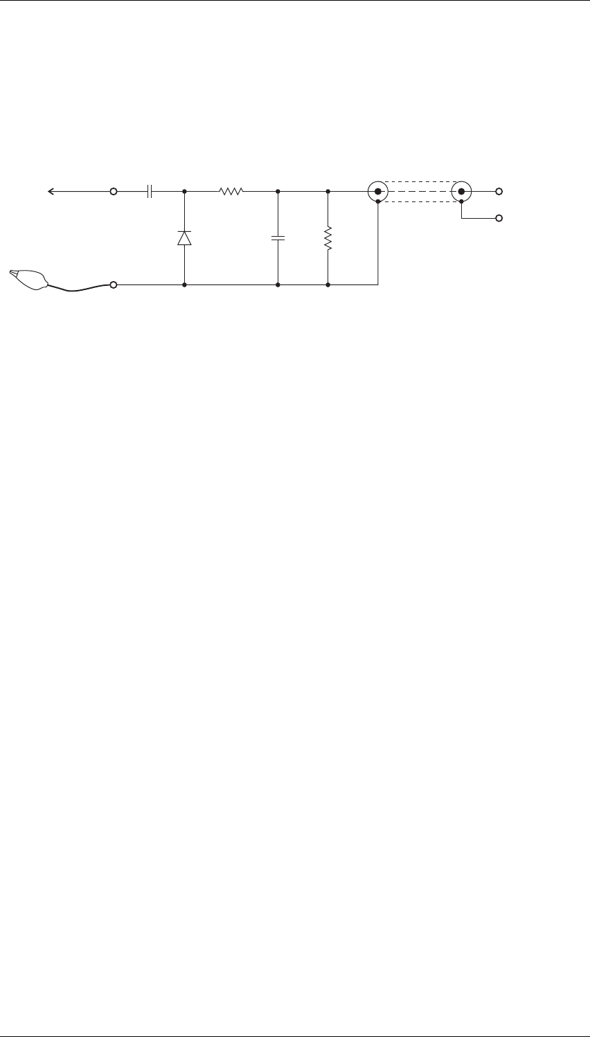
Figure 5.1 RF Diode Probe Circuit
5.5.1 Output Power
Refer to the exciter drive amplifier fault finding chart (Section 5.7.4).
Ensure that the VCO locks (refer to Section 5.4.2).
Connect the exciter output to a power meter and key the exciter.
Check that the output power is between 600 and 1000mW.
Note: If the synthesiser is out of lock, the lock detector (synthesiser IC740 and
comparator IC750) will prevent the RF signal from reaching the PA by
switching the supply to the exciter amplifier (Q340, Q345).
100k
10k
1n
1n
1N6263
Coax
Probe
Earthing Clip
DC to DVM or
Oscilloscope
This unit is not suitable for use on high power RF circuits.

C5.6 T837 Fault Finding M830P-00
01/07/00 Copyright TEL
5.6 PGM800Win Generated Errors
The following errors are those most likely to occur using PGM800Win. Refer to the
PGM800Win software user’s manual for a complete list of error messages.
Channel Switch Set
The programmed default channel change was not accepted by the base station because a
channel is selected externally. Try turning the external channel switch off to change the
default channel in PGM800Win.
Synth Out Of Lock
The synthesiser received incorrect data, or the data was corrupted. Enter a frequency
within the VCO switching range, or tune the VCO.
Internal Error
Data could not be read from the base station due to an internal error. Check for shorts
or open circuits on the SDA, SCK, SYNTH and EPOT lines. The SDA, SCK and SYNTH
are normally high.
Write/Read To An Unlinked Module
The link to the module does not exist. Undefined error.
M830P-00 T837 Fault Finding C5.7
Copyright TEL 01/07/00
5.7 Fault Finding Charts
Note: The standard test point designations used in this section are as follows:
TP601 13.8V
TP602 9V
TP603 20V
TP604 5V
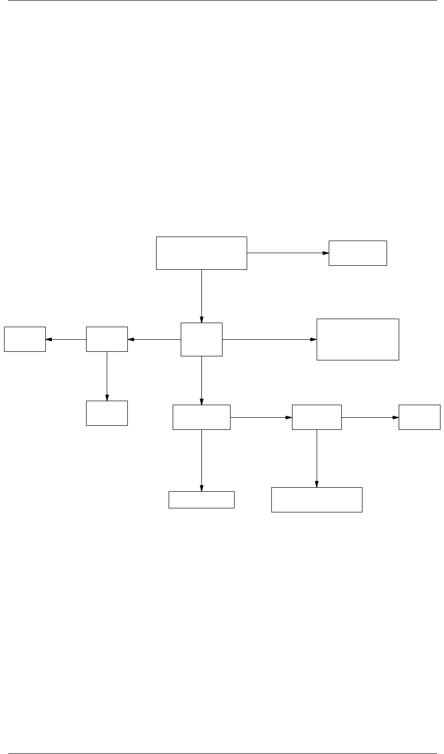
5.7.1 Microcontroller (IC810)
5.7.1.1 Basic Checks
Pulsing Check state
of pin 35.
Y
Is pin 30
pulsing?
High or open circuit
Y
Static high/low
Check state of
pins 36 to 43.
Low/floating
High
Is the 12.8MHz clock
present on IC810 pin 21
(microcontroller)?
N
Replace
IC810.
Check IC740
(synthesiser).
*digital storage oscilloscope
Replace IC810.
Check the
state of
pin 10.
N Pulsing
Low
Replace
IC810.
Use a DSO* to check
operation of IC650
(i.e. active high
pulse at power up).
Replace
IC650.
Correct the fault causing
pin 35 to be low/floating.
C5.8 T837 Fault Finding M830P-00
01/07/00 Copyright TEL
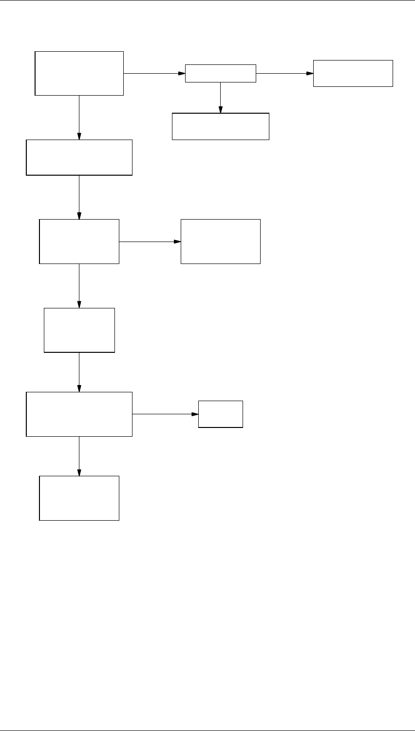
5.7.1.2 Serial Communication
Check pin state.
Y
Low/floating
N
Noise
on pin
Disconnect the
programming lead.
Is IC810 pin 11 high?
(microcontroller)
Y*digital storage
oscilloscope
Use PGM800Win
to send a POLL
command to the
radio.
Check the transistor
interface circuitry
and/or replace the
programming lead.
Check the SERIAL-COM
and AUDIO-1/2 links.
Replace
IC810.
Check the transistor
interface circuitry
and/or replace the
programming lead.
Check the transistor
interface circuitry.
Check IC810 pin 13
with a DSO. Is there
a response from IC810 after
a poll command is sent?
N
Y
Connect the programming
lead and use PGM800Win
to read the rack/radio.
Check I/O pad P810
with a DSO*.
Does it swing from
0 to 5V?
N
M830P-00 T837 Fault Finding C5.9
Copyright TEL 01/07/00
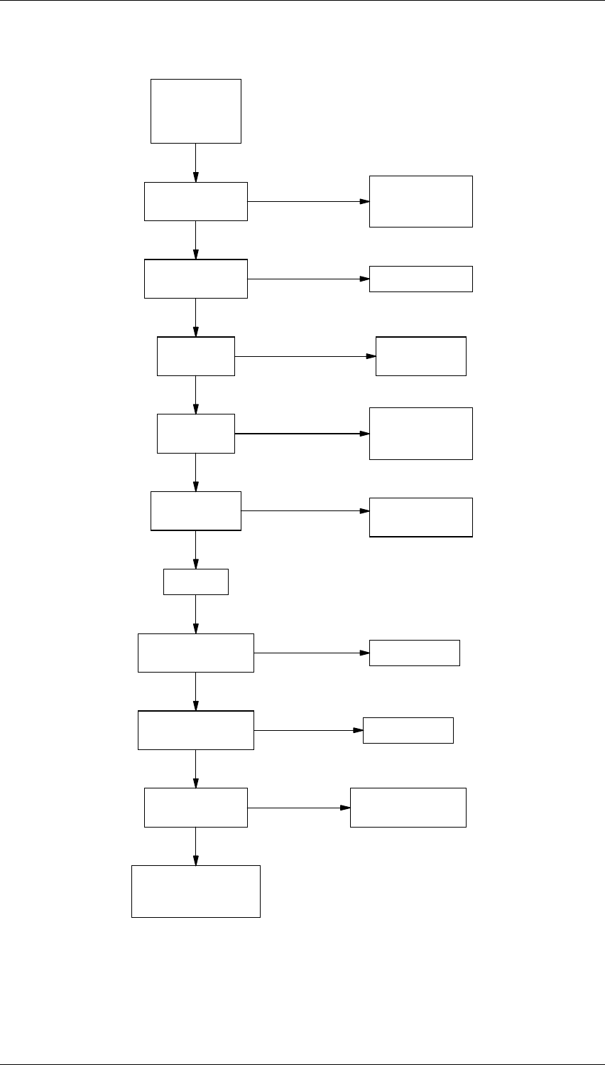
5.7.2 Regulator
N
Y
Check for
overheating
components &
short circuits.
N
Y
Check Q630,
Q620 & IC640.
N
Y
9.0V present
on TP602?
Check Q660 is
switching at
approx. 150kHz.
N
Y
20V present
on TP603?
Check R615.
Replace IC610.
N
Y
+5V present on
IC610 pin 2?
Key Tx.
YRegulators OK.
N
8.8V present
on Tx reg. TP305?
Replace Q610.
Y
N
0V present
on Q860 collector?
Check Q860 and
associated circuitry.
Y
0.6V present on
Q860 base?
N
Regulators OK.
Check microcontroller
section.
Check continuity
from pin 9 of
D-range 1.
13.8V present on
IC630 pin 3?
5.3V present on
IC630 pin 1? Replace IC630.
C5.10 T837 Fault Finding M830P-00
01/07/00 Copyright TEL
5.7.3 Synthesiser
Refer to the synthesiser circuit diagram (sheet 7) in Section 6 and the VCO circuit dia-
gram in Part E.
N
A B
Check biasing
resistors, Q4 & Q5.
N
Y
N
8.3V present
at VCO?
DC V present
at Q4 & Q5?
9V present at
VCO Q4/Q5?
No VCO RF output.
Y
DC V present at
VCO, Q1, Q2 & Q3?
Check biasing
resistors, Q1,
Q2 & Q3.
Y
N
Capacitors OK?
Check for cracks,
shorts, etc.
N
Y
Replace VCO.
Replace
if faulty.
Y
N
N
N
Y
Y
DC V present
on Q795 emitter?
Check 9V supply.
9V present on
Q795 divider buffer?
20V inverter
supply faulty.
20V present
on IC750 pin 8?
Check 5V reg. &
supply resistor
to each IC.
VCO out of lock.
Y
Y
Y
Continued on the next page
Y
Does VCO trimmer
adjust for stable
control line
between 5 & 13V?
VCO freq. correct?
Does VCO trimmer
adjust for required
frequency range
between 5 & 13V?
Synthesiser OK.
VCO trimmer
freq. range OK?
Check VCO tuning
caps & trimmer.
Is 8MHz VCO range
achieved between
5 & 13V?
VCO OK.
N
N
NN
N
Y
Y
Recheck
programming
via PGM800Win.
Check Q5 C
multiplier
(synth).
Check biasing
resistors & Q795.
Check #C5, #C3, #C4,
CV1 & D1-D4 in VCO.
Check Tx reg.,
Q610 & 9V reg. +5V present at
IC710 & IC740?
N
Y
M830P-00 T837 Fault Finding C5.11
Copyright TEL 01/07/00
Programming and
serial bus OK?
Check programming.
Check serial bus
when programming
i.e. clock/data/enable
activity (IC740 pins
18, 19 & 17). N
Check loop filter components
R775, C774, C776, R510,
C505, IC750. Is the supply
to IC750 +20V +4, -2V?
Check regulator circuitry.
Check C772, R774, R772,
C770, R763 & Q790.
Check Q760, Q780,
R766 & C765.
Check charge pump components
(Q775 & Q780) and Q790.
Check R762 & C762.
Check the signal path from
the VCO to synthesiser.
Measure the frequency from
the VCO at IC740 pin 11 using
a frequency counter.
Is the level >-10dBm?
Does the frequency adjust
as the VCO trimmer is
adjusted (out of lock)?
Check VCO.
Y
Y
Y
Signal
Y
Y
Y
No signal
Replace synthesiser
(IC740).
Y
N Y
Y
N
N
N
N
Check phase detector output
pins (IC740 pins 3 & 4).
Are there very narrow pulses
(~50ns) at the reference frequency?
(i.e. 5kHz : 200µs period
6.25kHz : 160µs period)
*See Note below.
Is the charge pump bias
voltage at the base of
Q760 & Q780 between
3.5 and 5V? (5V when locked)
N
Is the voltage on C762,
R760, and R758 9V ±0.2V?
Is the loop filter reference
voltage at C772 (+) 6.5V ±0.2V?
N
Check divider buffer
circuit (Q795) and bias
voltages on Q795 emitter
(1.3V ±0.2V).
*Note:
When locked, both of these
are very narrow (~50ns).
If unlocked, one will be
very narrow (~50ns),
and the other wide (>15µs).
Replace synthesiser
(IC740).
Continued from previous page
B
Is the charge pump voltage
on Q790 gate between
3 and 8.5V? (6.5V ±0.2V locked)
Check microcontroller
section (IC810).
N
N
Y
Is reference
clock present
at IC740 pin 20
(12.8MHz >4.5Vpp)?
Is reference
clock present
at IC710 pins 5 & 13
(12.8MHz >4.5Vpp)?
Y
Is reference
clock present
at IC102 pin 6
in modulator section
(12.8MHz >4.0Vpp)?
N
Check VCXO (X101)
and buffers (IC102).
Check IC710, R710,
C712, C713, C733.
Check line from
modulator section to
synthesiser section.
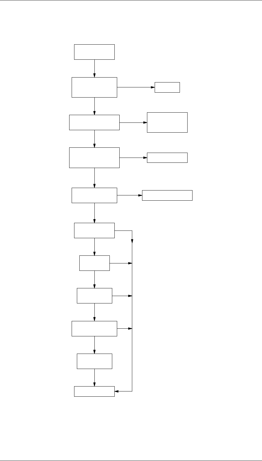
C5.12 T837 Fault Finding M830P-00
01/07/00 Copyright TEL
Y
N
Y
Y
VCO phase locked?
5-13V present on
control line?
Correct DC V
present on Q1 VCO?
N
Check inductors,
biasing resistors
& Q1.
Replace if faulty.
Go to B.
Loop filter &
components around
op. amp. (IC750) OK?
N
Noisy synth;
poor residual FM.
C
Y
Y
N
Y
Y
Y
Change trimmer;
still noisy?
Change Q1;
still noisy?
Change TCXO;
still noisy?
Change varactors;
still noisy?
Replace VCO
assembly.
Synthesiser OK.
N
N
N
N
Isolate modulation
on VCO; still noisy?
Y
Trace modulator fault.

M830P-00 T837 Fault Finding C5.13
Copyright TEL 01/07/00
5.7.4 Exciter Drive Amplifier
10.5V at Q315
collector?
Check IC330,
R324 & R326.
Check Q310
& Q315.
>0.5V RF at
Q365 base?
>1.5V RF at
Q370 base?
Check Q365.
Check signal path
between Q365 & Q370.
Check Q370.
3.5V at Q365 collector?
10.5V at Q370 collector? Check
power rails.
>5V present on
IC330 pin 1?
Key exciter &
lock synthesiser.
Check VCO.
>6V RF at
Q370 collector?
Drive amp. OK.
NY
YN
N
Y
N
Y
N
Y
N
Y
N
Y
N
Y
N
Y
>2.2V RF at
R359/R342?
>1.1V RF at
R342/R344? Check attenuator pad
R359, R342, R344.
Check C352, C355, C358,
Q365, L345, L346, D340,
D350, & D360.
>6V RF at
C361, L360?

C5.14 T837 Fault Finding M830P-00
01/07/00 Copyright TEL
M830P-00 T837 PCB Information C6.1.1
Copyright TEL 01/07/00
6 T837 PCB Information
Caution: This equipment contains CMOS devices which are susceptible to damage from
static charges. Refer to Section 1.2 in Part A for more information on anti-static
procedures when handling these devices.
This section provides the following information on the T837 paging exciter:
•parts lists
• grid reference index
•PCB layouts
• circuit diagrams.
Section Title IPN Page
6.1 Introduction 6.1.3
6.2 T837 Paging Exciter PCB 220-01585-01 6.2.1

C6.1.2 T837 PCB Information M830P-00
01/07/00 Copyright TEL
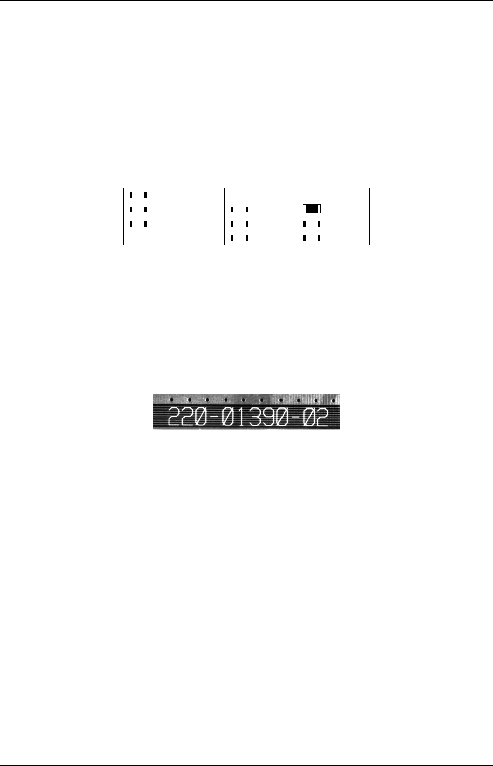
M830P-00 T837 PCB Information C6.1.3
Copyright TEL 01/07/00
6.1 Introduction
Product Type Identification
You can identify the exciter type by checking the product code printed on a label on the rear of the
chassis (product codes are explained in Section 1.3 in this Part of the manual, and Figure 1.1 in Part
A shows typical labels). You can further verify the product type by checking the placement of an
SMD resistor in the table that is screen printed onto the top side of the PCB, similar to the example
drawn below. In this example, the resistor indicates that the product was built as a T837-20-XXXX.
Note: The only function of this resistor is to indicate the product type. It has no effect on the
circuitry or operation of the exciter.
PCB Identification
All PCBs are identified by a unique 10 digit “internal part number” (IPN), e.g. 220-12345-00, which
is screen printed onto the PCB (usually on the top side), as shown in the example below:
The last 2 digits of this number define the issue status, which starts at 00 and increments through 01,
02, 03, etc. as the PCB is updated. Some issue PCBs never reach full production status and are there-
fore not included in this manual. A letter following the 10 digit IPN has no relevance in identifying
the PCB for service purposes.
Note: It is important that you identify which issue PCB you are working on so that you can
refer to the appropriate set of PCB information.
837- PRODUCT TYPE
837- 837-10 837-20
837- 837-13 837-23
PRODUCT TYPE 837-15 837-25

C6.1.4 T837 PCB Information M830P-00
01/07/00 Copyright TEL
Parts Lists
The 10 digit numbers (000-00000-00) in this Parts List are “internal part numbers” (IPNs). We can
process your spare parts orders more efficiently and accurately if you quote the IPN and provide a
brief description of the part.
The components listed in this parts list are divided into two main types: those with a circuit refer-
ence (e.g. C2, D1, R121, etc.) and those without (miscellaneous and mechanical).
Those with a circuit reference are grouped in alphabetical order and then in numerical order within
each group. Each component entry comprises three or four columns, as shown below:
The mechanical and miscellaneous section lists the variant and common parts in IPN order.
Parts List Amendments
At the front of the parts list is the Parts List Amendments box (an example of which is shown
below). This box contains a list of component changes which took place after the parts list and dia-
grams in this section were compiled. These changes (e.g. value changes, added/deleted compo-
nents, etc.) are listed by circuit reference in alphanumeric order and supersede the information
given in the parts list or diagrams. Components without circuit references are listed in IPN order.
The number in brackets at the end of each entry refers to the Tait internal Change Order document.
circuit reference -
lists components
in alphanumeric
order
variant column -
indicates that this is
a variant component
which is fitted only to
the product type listed
Internal Part Number -
order the component
b
y
this number
description -
gives a brief description
of the component
Parts List Amendments
R306 Changed from 180Ωto 560Ω(036-13560-00) to increase sensitivity (71003).
circuit reference
or IPN description
of change
IPN of new
component Change Order
number

M830P-00 T837 PCB Information C6.1.5
Copyright TEL 01/07/00
Variant Components
A variant component is one that has the same circuit reference but different value or specification in
different product types. Where two products share the same PCB, the term “variant” is also used to
describe components unplaced in one product. Variant components have a character prefix, such as
“&”, “=” or “#”, before the circuit reference (e.g. &R100).
The table below explains the variant prefixes used in T800 Series II products:
Grid Reference Index
This section contains a component grid reference index to help you find components and labelled
pads on the PCB layouts and circuit diagrams. This index lists the components and pads in alpha-
numeric order, along with the appropriate alphanumeric grid references, as shown below:
If the variant prefix is. . . the component will. . .
& change according to channel spacing
= change according to frequency stability
# change according to frequency range
% change or be placed/unplaced for special applications
*be unplaced in one product
(where two products share the same PCB)
circuit diagram
reference
PCB layout
reference
components listed
in alphanumeric order
layer number -
1 = top side layer
2 = bottom side layer
component location
on the layer
sheet number
component location
on the sheet

C6.1.6 T837 PCB Information M830P-00
01/07/00 Copyright TEL
Using CAD Circuit Diagrams
Reading a CAD circuit diagram is similar to reading a road map, in that both have an alphanumeric
border. The circuit diagrams in this manual use letters to represent the horizontal axis, and num-
bers for the vertical axis. These circuit diagram “grid references” are useful in following a circuit
that is spread over two or more sheets.
When a line representing part of the circuitry is discontinued, a reference will be given at the end of
the line to indicate where the rest of the circuitry is located, as shown below. The first digit refers to
the sheet number and the last two characters refer to the location on that sheet of the continuation of
the circuit (e.g. 1R3).
C301
4N7
R303
12
D
S
G
L310
33U
IF-SIG
4R4
C369
100P
C371
10U
R339
100K
%R338
100
DISCRIMINATOR
1R3
2R9
2R9
8A2
t
hese grid references
s
how where the circuit
is continued

M830P-00 T837 PCB Information C6.2.1
Copyright TEL 01/07/00
6.2 T837 Paging Exciter PCB
This section contains the following information.
IPN Section Page
220-011585-01 Parts List
Mechanical & Miscellaneous Parts
Grid Reference Index
PCB Layout - Top Side
PCB Layout - Bottom Side
Exciter Overview Diagram
Low Speed Paging Modulator Circuit Diagram
Exciter Circuit Diagram
VCO Section Circuit Diagram
Regulators Circuit Diagram
Synthesiser Circuit Diagram
Microcontroller Circuit Diagram
Harmonic Filter Circuit Diagram
6.2.5
6.2.9
6.2.10
6.2.13
6.2.14
6.2.15
6.2.16
6.2.17
6.2.19
6.2.20
6.2.21
6.2.22
6.2.23

C6.2.2 T837 PCB Information M830P-00
01/07/00 Copyright TEL

IPN 220-01585-01
M830P-00 T837 PCB Information C6.2.3
Copyright TEL 01/07/00
T837 Parts List (IPN 220-01585-01)
How To Use This Parts List
The components listed in this parts list are divided into two main types: those with a circuit reference (e.g. C2, D1, R121, etc.) and
those without (miscellaneous and mechanical).
Those with a circuit reference are grouped in alphabetical order and then in numerical order within each group. Each component
entry comprises three or four columns: the circuit reference, variant (if applicable), IPN and description. A number in the variant col-
umn indicates that this is a variant component which is fitted only to the product type listed. Static sensitive devices are indicated by
an (S) at the start of the description column.
The miscellaneous and mechanical section lists the variant and common parts in IPN order. Where possible, a number in the legend
column indicates their position in the mechanical assembly drawing.
The Parts List Amendments box below lists component changes that took place after the parts list and diagrams in this section were
compiled. These changes (e.g. value changes, added/deleted components, etc.) are listed by circuit reference in alphanumeric order
and supersede the information given in the parts list or diagrams. Components without circuit references are listed in IPN order.
Parts List Amendments
There were no amendments to the parts list at the time of publication.

IPN 220-01585-01
C6.2.4 T837 PCB Information M830P-00
01/07/00 Copyright TEL
Parts List Amendments - Continued
This page is provided for entering future amendments to the parts list.

IPN 220-01585-01
M830P-00 T837 PCB Information C6.2.5
Copyright TEL 01/07/00
Ref Var IPN Description Ref Var IPN Description
C100 014-08100-00 CAP TANT CHIP 10M 16VW +-20%
C101 014-08100-00 CAP TANT CHIP 10M 16VW +-20%
C102 015-24100-08 CAP CER 0805 1N 10% X7R 50V
C103 015-24100-08 CAP CER 0805 1N 10% X7R 50V
C104 015-24100-08 CAP CER 0805 1N 10% X7R 50V
C105 015-24100-08 CAP CER 0805 1N 10% X7R 50V
C106 015-24100-08 CAP CER 0805 1N 10% X7R 50V
*C107 20-1021 015-25470-08 CAP CER 0805 47N 10% X7R 50V
*C107 26-1021 015-25470-08 CAP CER 0805 47N 10% X7R 50V
C108 015-21820-02 CAP 0805 8P2 0.1 NPO 50V
C109 015-22470-01 CAP CER 0805 47P 5% NPO 50V
*C110 20-1021 015-25100-08 CAP CER 0805 10N 10% X7R 50V
*C110 26-1021 015-25100-08 CAP CER 0805 10N 10% X7R 50V
*C111 20-1021 015-24100-08 CAP CER 0805 1N 10% X7R 50V
*C111 26-1021 015-24100-08 CAP CER 0805 1N 10% X7R 50V
C112 015-24100-08 CAP CER 0805 1N 10% X7R 50V
%C113 20-1020 015-25100-08 CAP CER 0805 10N 10% X7R 50V
%C113 20-1021 015-25100-08 CAP CER 0805 10N 10% X7R 50V
%C113 26-1020 015-24680-08 CAP CER 0805 6N8 10% X7R 50V
%C113 26-1021 015-24680-08 CAP CER 0805 6N8 10% X7R 50V
C115 015-21820-02 CAP 0805 8P2 0.1 NPO 50V
*C122 20-1021 015-25100-08 CAP CER 0805 10N 10% X7R 50V
*C122 26-1021 015-25100-08 CAP CER 0805 10N 10% X7R 50V
C123 015-24100-08 CAP CER 0805 1N 10% X7R 50V
*C124 20-1021 015-24100-08 CAP CER 0805 1N 10% X7R 50V
*C124 26-1021 015-24100-08 CAP CER 0805 1N 10% X7R 50V
%C125 20-1020 015-24220-08 CAP CER 0805 2N2 10% X7R 50V
%C125 20-1021 015-24220-08 CAP CER 0805 2N2 10% X7R 50V
*C126 20-1021 015-24100-08 CAP CER 0805 1N 10% X7R 50V
*C126 26-1021 015-24100-08 CAP CER 0805 1N 10% X7R 50V
*C127 20-1021 015-25100-08 CAP CER 0805 10N 10% X7R 50V
*C127 26-1021 015-25100-08 CAP CER 0805 10N 10% X7R 50V
%C128 20-1020 015-24100-08 CAP CER 0805 1N 10% X7R 50V
%C128 20-1021 015-24100-08 CAP CER 0805 1N 10% X7R 50V
%C128 26-1020 015-24100-08 CAP CER 0805 1N 10% X7R 50V
%C128 26-1021 015-24100-08 CAP CER 0805 1N 10% X7R 50V
%C129 20-1020 015-25220-08 CAP CER 0805 22N 10% X7R 50V
%C129 20-1021 015-25220-08 CAP CER 0805 22N 10% X7R 50V
%C129 26-1020 015-24220-08 CAP CER 0805 2N2 10% X7R 50V
%C129 26-1021 015-24220-08 CAP CER 0805 2N2 10% X7R 50V
*C130 20-1021 014-08100-00 CAP TANT CHIP 10M 16VW +-20%
*C130 26-1021 014-08100-00 CAP TANT CHIP 10M 16VW +-20%
*C131 20-1021 015-25100-08 CAP CER 0805 10N 10% X7R 50V
*C131 26-1021 015-25100-08 CAP CER 0805 10N 10% X7R 50V
*C132 20-1021 014-07470-01 CAP 4U7 ’B’CASE 25V +-10% 267
*C132 26-1021 014-07470-01 CAP 4U7 ’B’CASE 25V +-10% 267
*C133 20-1021 015-24470-08 CAP CER 0805 4N7 10% X7R 50V
*C133 26-1021 015-24470-08 CAP CER 0805 4N7 10% X7R 50V
*C134 20-1021 013-06100-10 CAP SMD PPS 100N 100V 10%
*C134 26-1021 013-06100-10 CAP SMD PPS 100N 100V 10%
*C135 20-1021 015-24470-08 CAP CER 0805 4N7 10% X7R 50V
*C135 26-1021 015-24470-08 CAP CER 0805 4N7 10% X7R 50V
*%C136 20-1021 015-24100-08 CAP CER 0805 1N 10% X7R 50V
*%C136 26-1020 015-24100-08 CAP CER 0805 1N 10% X7R 50V
*%C136 26-1021 015-24100-08 CAP CER 0805 1N 10% X7R 50V
%C137 20-1020 036-10000-00 RES M/F 0805 ZERO OHM
%C137 20-1021 015-24680-08 CAP CER 0805 6N8 10% X7R 50V
%C137 26-1020 015-24680-08 CAP CER 0805 6N8 10% X7R 50V
%C137 26-1021 015-24680-08 CAP CER 0805 6N8 10% X7R 50V
C138 015-24330-08 CAP CER 0805 3N3 10% X7R 50V
C139 015-24330-08 CAP CER 0805 3N3 10% X7R 50V
*C140 20-1021 015-25100-08 CAP CER 0805 10N 10% X7R 50V
*C140 26-1021 015-25100-08 CAP CER 0805 10N 10% X7R 50V
C141 015-24220-08 CAP CER 0805 2N2 10% X7R 50V
C142 015-24220-08 CAP CER 0805 2N2 10% X7R 50V
*C143 20-1021 015-25100-08 CAP CER 0805 10N 10% X7R 50V
*C143 26-1021 015-25100-08 CAP CER 0805 10N 10% X7R 50V
C144 015-23100-01 CAP CER 0805 100P 5% NPO 50V
*C145 20-1021 014-07470-01 CAP 4U7 ’B’CASE 25V +-10% 267
*C145 26-1021 014-07470-01 CAP 4U7 ’B’CASE 25V +-10% 267
*C146 20-1021 014-08100-00 CAP TANT CHIP 10M 16VW +-20%
*C146 26-1021 014-08100-00 CAP TANT CHIP 10M 16VW +-20%
*C147 20-1021 015-06100-08 CAP CER 1206 100N 10% X7R 50V
*C147 26-1021 015-06100-08 CAP CER 1206 100N 10% X7R 50V
C148 014-08100-00 CAP TANT CHIP 10M 16VW +-20%
C149 015-25100-08 CAP CER 0805 10N 10% X7R 50V
C150 014-08100-00 CAP TANT CHIP 10M 16VW +-20%
C151 015-25100-08 CAP CER 0805 10N 10% X7R 50V
C152 013-06470-00 CAP SMD POLYESTER 470N 63V 10%
C153 013-06470-00 CAP SMD POLYESTER 470N 63V 10%
C154 015-25100-08 CAP CER 0805 10N 10% X7R 50V
C155 015-06100-08 CAP CER 1206 100N 10% X7R 50V
C156 015-25100-08 CAP CER 0805 10N 10% X7R 50V
*C157 20-1021 015-25100-08 CAP CER 0805 10N 10% X7R 50V
*C157 26-1021 015-25100-08 CAP CER 0805 10N 10% X7R 50V
C158 015-25100-08 CAP CER 0805 10N 10% X7R 50V
C159 014-08100-00 CAP TANT CHIP 10M 16VW +-20%
C160 015-25100-08 CAP CER 0805 10N 10% X7R 50V
C161 014-08100-00 CAP TANT CHIP 10M 16VW +-20%
C162 015-25100-08 CAP CER 0805 10N 10% X7R 50V
C163 015-23100-01 CAP CER 0805 100P 5% NPO 50V
C164 014-08100-00 CAP TANT CHIP 10M 16VW +-20%
*C165 20-1021 015-25100-08 CAP CER 0805 10N 10% X7R 50V
*C165 26-1021 015-25100-08 CAP CER 0805 10N 10% X7R 50V
C166 015-25100-08 CAP CER 0805 10N 10% X7R 50V
C167 014-08100-00 CAP TANT CHIP 10M 16VW +-20%
C168 014-08100-00 CAP TANT CHIP 10M 16VW +-20%
*C169 20-1021 014-08100-00 CAP TANT CHIP 10M 16VW +-20%
*C169 26-1021 014-08100-00 CAP TANT CHIP 10M 16VW +-20%
C170 014-08100-00 CAP TANT CHIP 10M 16VW +-20%
*C171 20-1021 014-08100-00 CAP TANT CHIP 10M 16VW +-20%
*C171 26-1020 014-08100-00 CAP TANT CHIP 10M 16VW +-20%
*C171 26-1021 014-08100-00 CAP TANT CHIP 10M 16VW +-20%
C172 015-06100-08 CAP CER 1206 100N 10% X7R 50V
*C173 20-1021 015-06100-08 CAP CER 1206 100N 10% X7R 50V
*C173 26-1020 015-06100-08 CAP CER 1206 100N 10% X7R 50V
*C173 26-1021 015-06100-08 CAP CER 1206 100N 10% X7R 50V
C301 015-24470-08 CAP CER 0805 4N7 10% X7R 50V
C304 015-24100-08 CAP CER 0805 1N 10% X7R 50V
C307 015-25100-08 CAP CER 0805 10N 10% X7R 50V
C309 015-23680-08 CAP CER 0805 680P 10% X7R 50V
C310 015-24100-08 CAP CER 0805 1N 10% X7R 50V
C313 015-24100-08 CAP CER 0805 1N 10% X7R 50V
C317 015-23100-01 CAP CER 0805 100P 5% NPO 50V
C318 015-23100-01 CAP CER 0805 100P 5% NPO 50V
C319 015-24100-08 CAP CER 0805 1N 10% X7R 50V
C325 015-24100-08 CAP CER 0805 1N 10% X7R 50V
C328 015-25470-08 CAP CER 0805 47N 10% X7R 50V
C330A 015-25100-08 CAP CER 0805 10N 10% X7R 50V
C330B 014-08100-03 CAP TANT SMD 10U 35V 20%
C331 015-24100-08 CAP CER 0805 1N 10% X7R 50V
C334 014-07470-04 CAP TANT SMD 4U7 50V 20%
C337 015-24100-08 CAP CER 0805 1N 10% X7R 50V
C340 015-24100-08 CAP CER 0805 1N 10% X7R 50V
C343 015-24100-08 CAP CER 0805 1N 10% X7R 50V
C346 015-24100-08 CAP CER 0805 1N 10% X7R 50V
C349 015-23150-01 CAP CER 0805 150P 5% NPO 50V
C352 015-24100-08 CAP CER 0805 1N 10% X7R 50V
C355 015-22330-01 CAP CER 0805 33P 5% NPO 50V
C358 015-22820-01 CAP CER 0805 82P 5% NPO 50V
C361 015-24100-08 CAP CER 0805 1N 10% X7R 50V
C376 015-04100-04 CAP CER 1206 1N 10% X7R 50V
C379 015-04100-04 CAP CER 1206 1N 10% X7R 50V
C382 015-24100-08 CAP CER 0805 1N 10% X7R 50V
C383 015-24100-08 CAP CER 0805 1N 10% X7R 50V
C384 015-22470-01 CAP CER 0805 47P 5% NPO 50V
C385 015-24100-08 CAP CER 0805 1N 10% X7R 50V
C388 015-24100-08 CAP CER 0805 1N 10% X7R 50V
C390 015-25100-08 CAP CER 0805 10N 10% X7R 50V
C391 015-21820-02 CAP 0805 8P2 0.1 NPO 50V
C392 015-25220-08 CAP CER 0805 22N 10% X7R 50V
C393 015-06100-08 CAP CER 1206 100N 10% X7R 50V
C394 015-24100-08 CAP CER 0805 1N 10% X7R 50V
C395 015-24100-08 CAP CER 0805 1N 10% X7R 50V
C397 015-24100-08 CAP CER 0805 1N 10% X7R 50V
C398 015-24100-08 CAP CER 0805 1N 10% X7R 50V
C503 015-24470-08 CAP CER 0805 4N7 10% X7R 50V
C505 015-06100-08 CAP CER 1206 100N 10% X7R 50V
C510 015-25220-08 CAP CER 0805 22N 10% X7R 50V
C513 015-25100-08 CAP CER 0805 10N 10% X7R 50V
C535 015-06100-08 CAP CER 1206 100N 10% X7R 50V
C550 014-08220-01 CAP TANT 22UF 10V 276MSER
C605 015-23120-01 CAP CER 0805 120P 5% NPO 50V
C610A 015-25100-08 CAP CER 0805 10N 10% X7R 50V
C610B 014-09100-00 CAP TANT SMD 100U 16V 20%
C611A 014-09100-00 CAP TANT SMD 100U 16V 20%
C611B 015-25100-08 CAP CER 0805 10N 10% X7R 50V
C623 015-23120-01 CAP CER 0805 120P 5% NPO 50V
C625 020-09470-07 CAP ELEC RADL 470M 16V 20% 3.5
C626 015-24470-08 CAP CER 0805 4N7 10% X7R 50V
C628 015-24100-08 CAP CER 0805 1N 10% X7R 50V
C630 015-06100-08 CAP CER 1206 100N 10% X7R 50V
C631 015-06100-08 CAP CER 1206 100N 10% X7R 50V
C634 014-08100-00 CAP TANT CHIP 10M 16VW +-20%
C636 015-06100-08 CAP CER 1206 100N 10% X7R 50V
C638 015-23120-01 CAP CER 0805 120P 5% NPO 50V
C640 015-24100-08 CAP CER 0805 1N 10% X7R 50V
C660 015-06100-08 CAP CER 1206 100N 10% X7R 50V
C665 014-08100-03 CAP TANT SMD 10U 35V 20%
C670 014-07330-10 CAP TANT SMD 3U3 35V 10%
Note: The T837-2X-1020 and T837-2X-1021 share the same
basic design and are built on the same PCB. However,
there are a number of special variant components in
these products.
The “*” variant prefix is used to indicate those compo-
nents which are placed only in the T837-2X-1021.
The “%” prefix indicates components which are placed
in all product types, but may have different values in
each product type.
The “*%” prefixes indicate components which are
optional in the T837-2X-1021 only, and not placed at all
in the T837-2X-1020.

IPN 220-01585-01
C6.2.6 T837 PCB Information M830P-00
01/07/00 Copyright TEL
Ref Var IPN Description Ref Var IPN Description
C673 015-24470-08 CAP CER 0805 4N7 10% X7R 50V
C677 014-07100-02 CAP TANT CHIP 1U0 3.2X1.6M 16V
C681 015-06100-08 CAP CER 1206 100N 10% X7R 50V
C684 014-08100-00 CAP TANT CHIP 10M 16VW +-20%
C687 015-23120-01 CAP CER 0805 120P 5% NPO 50V
C690 015-06100-08 CAP CER 1206 100N 10% X7R 50V
C693 014-08100-00 CAP TANT CHIP 10M 16VW +-20%
C706 015-22470-01 CAP CER 0805 47P 5% NPO 50V
C708 014-07470-01 CAP 4U7 ’B’CASE 25V +-10% 267
C709 015-06100-08 CAP CER 1206 100N 10% X7R 50V
C710 015-25100-08 CAP CER 0805 10N 10% X7R 50V
C712 015-22470-01 CAP CER 0805 47P 5% NPO 50V
C713 015-25100-08 CAP CER 0805 10N 10% X7R 50V
C714 014-07470-01 CAP 4U7 ’B’CASE 25V +-10% 267
C733 015-21470-01 CAP CER 0805 4P7+-0.25 NPO 50V
C735 015-22470-01 CAP CER 0805 47P 5% NPO 50V
C736 015-22470-01 CAP CER 0805 47P 5% NPO 50V
C740A 015-24100-08 CAP CER 0805 1N 10% X7R 50V
C740B 015-25100-08 CAP CER 0805 10N 10% X7R 50V
C741A 014-07470-01 CAP 4U7 ’B’CASE 25V +-10% 267
C741B 015-25100-08 CAP CER 0805 10N 10% X7R 50V
C742A 015-06100-08 CAP CER 1206 100N 10% X7R 50V
C742B 015-25100-08 CAP CER 0805 10N 10% X7R 50V
C743 015-22470-01 CAP CER 0805 47P 5% NPO 50V
C745 015-24100-08 CAP CER 0805 1N 10% X7R 50V
C750 014-08100-03 CAP TANT SMD 10U 35V 20%
C757 015-06100-08 CAP CER 1206 100N 10% X7R 50V
C759 015-06100-08 CAP CER 1206 100N 10% X7R 50V
C761 015-25100-08 CAP CER 0805 10N 10% X7R 50V
C762 014-08220-01 CAP TANT 22UF 10V 276MSER
C764 015-25100-08 CAP CER 0805 10N 10% X7R 50V
C765 014-07470-01 CAP 4U7 ’B’CASE 25V +-10% 267
C767 015-24100-08 CAP CER 0805 1N 10% X7R 50V
C769 015-24100-08 CAP CER 0805 1N 10% X7R 50V
C770 014-08220-01 CAP TANT 22UF 10V 276MSER
C772 014-08220-01 CAP TANT 22UF 10V 276MSER
C774 013-06330-11 CAP SMD PPS 330N 63V 5%
C776 015-25150-08 CAP CER 0805 15N 10% X7R 50V
C782 015-24100-08 CAP CER 0805 1N 10% X7R 50V
C784 015-24100-08 CAP CER 0805 1N 10% X7R 50V
C786 015-06100-08 CAP CER 1206 100N 10% X7R 50V
C788 015-24100-08 CAP CER 0805 1N 10% X7R 50V
C790 015-24100-08 CAP CER 0805 1N 10% X7R 50V
C792 015-24100-08 CAP CER 0805 1N 10% X7R 50V
C810 015-25470-08 CAP CER 0805 47N 10% X7R 50V
C812 015-23100-01 CAP CER 0805 100P 5% NPO 50V
C813 015-24100-08 CAP CER 0805 1N 10% X7R 50V
C910 015-02120-06 CAP CER 1210 12P NPO500VGRM42
C920 015-02270-06 CAP CER 1210 27P NPO 500V
C930 015-02120-06 CAP CER 1210 12P NPO500VGRM42
%D1 20-1020 001-10015-50 DIODE SMD ZENER 1.5SMC22AT3
%D1 20-1021 001-10015-50 DIODE SMD ZENER 1.5SMC22AT3
%D1 26-1020 001-10015-50 DIODE SMD ZENER 1.5SMC22AT3
%D1 26-1021 001-10015-50 DIODE SMD ZENER 1.5SMC22AT3
*D100 20-1021 001-10000-70 S) DIODE SMD BAV70 D-SW SOT23
*D100 26-1021 001-10000-70 S) DIODE SMD BAV70 D-SW SOT23
D105 001-10000-70 S) DIODE SMD BAV70 D-SW SOT23
*D116 20-1021 008-10067-03 S) LED SMD GRN LGT670-HK
*D116 26-1021 008-10067-03 S) LED SMD GRN LGT670-HK
D119 008-00014-80 S)LED 3MM GREEN WITH WIRE
D120 001-10000-70 S) DIODE SMD BAV70 D-SW SOT23
D125 008-00014-79 S)LED 3MM RED WITH WIRE
D130 001-10000-70 S) DIODE SMD BAV70 D-SW SOT23
D135 001-10000-70 S) DIODE SMD BAV70 D-SW SOT23
D140 001-10000-70 S) DIODE SMD BAV70 D-SW SOT23
D160 001-10000-70 S) DIODE SMD BAV70 D-SW SOT23
*D200 20-1021 001-10000-70 S) DIODE SMD BAV70 D-SW SOT23
*D200 26-1021 001-10000-70 S) DIODE SMD BAV70 D-SW SOT23
*D220 20-1021 001-10000-99 S) DIODE SMD BAV99 D-SW SOT23
*D220 26-1021 001-10000-99 S) DIODE SMD BAV99 D-SW SOT23
D340 001-10000-18 S) DIODE SMD BAT18 S-SW SOT23
D350 001-10000-18 S) DIODE SMD BAT18 S-SW SOT23
D360 001-10000-18 S) DIODE SMD BAT18 S-SW SOT23
D370 001-10010-40 DIODE SMD ZENER 33V BZG03-C33
D610 001-10000-99 S) DIODE SMD BAV99 D-SW SOT23
D640 001-10000-70 S) DIODE SMD BAV70 D-SW SOT23
D645 001-10010-40 DIODE SMD ZENER 33V BZG03-C33
D730 001-10165-00 DIODE BAT165 SCHOTTKY SOD-323
D740 001-10165-00 DIODE BAT165 SCHOTTKY SOD-323
IC100 002-74910-04 S) IC SMD 74HCU04 6X INV
IC102 002-74910-04 S) IC SMD 74HCU04 6X INV
IC105 002-74901-09 S) IC SMD 74HC109 DUAL JK F/F
IC110 002-74901-09 S) IC SMD 74HC109 DUAL JK F/F
IC115 002-74900-86 S) IC SMD 74HC86 EX OR SO14
IC120 002-10006-60 S) IC SMD LMC660CM O-AMP 4X
IC125 002-10006-60 S) IC SMD LMC660CM O-AMP 4X
IC140 002-10041-04 S) IC SMD 4104 4X VOLT SHIFTER
IC150 002-10040-53 S)IC 4053B SMD BREAK B4 MAKE
*IC160 20-1021 002-10040-53 S)IC 4053B SMD BREAK B4 MAKE
*IC160 26-1021 002-10040-53 S)IC 4053B SMD BREAK B4 MAKE
*IC200 20-1021 002-14515-00 LIM)IC MC145151DW2 SYNTH P-IP
*IC200 26-1021 002-14515-00 LIM)IC MC145151DW2 SYNTH P-IP
*IC210 20-1021 002-10006-62 S)IC SMD LMC662CM 2X O-AMP
*IC210 26-1021 002-10006-62 S)IC SMD LMC662CM 2X O-AMP
*IC220 20-1021 002-74910-04 S) IC SMD 74HCU04 6X INV
*IC220 26-1021 002-74910-04 S) IC SMD 74HCU04 6X INV
*IC230 20-1021 002-10006-62 S)IC SMD LMC662CM 2X O-AMP
*IC230 26-1020 002-10006-62 S)IC SMD LMC662CM 2X O-AMP
*IC230 26-1021 002-10006-62 S)IC SMD LMC662CM 2X O-AMP
IC240 002-10006-60 S) IC SMD LMC660CM O-AMP 4X
IC250 002-10078-00 S)IC SMD MC78M05CDT 5V REG0.5A
IC330 002-10003-58 S) IC SMD LM358 DUAL O-AMP
IC610 002-10078-05 S) IC SMD 78L05 5V REG
IC630 002-10003-17 (S) IC LM317L REG S0-8 100MA
IC640 002-10003-58 S) IC SMD LM358 DUAL O-AMP
IC650 002-10012-32 SMD DS1232LPS-2 LP RESET&W-DOG
IC710 002-74900-04 S) IC SMD 74HC04D 6X INV BUFFD
IC740 002-14519-10 S) IC MC145191F SMD SYNTH
IC750 002-10330-78 S) IC MC33078D 2X AMP LO NOISE
IC810 002-08951-20 S) IC AT89C51 PLCC44 MIC 12MHZ
IC820 002-12416-00 S)IC SMD AT24C16N-10SC EEPROM
L335 056-10330-02 IND SMD 330NH SIMID02
L340 056-10330-02 IND SMD 330NH SIMID02
L345 052-08135-25 COIL A/W 2.5T/3.5MM HOR 0.8MM
L346 052-08125-15 COIL A/W 1.5T/2.5MM HOR 0.8MM
L355 056-14150-02 IND SMD 1.5UH SIMID02
L360 052-08135-35 COIL A/W 3.5T/3.5MM HOR 0.8MM
L365 052-08140-15 COIL A/W 1.5T/4.0MM HOR 0.8MM
L370 065-10009-20 BEAD FER SMD BDS 3/3/8.9-4S2
L375 065-10004-20 BEAD FE SMD CBD 4.6/3/3-4S2
L380 056-14150-02 IND SMD 1.5UH SIMID02
L385 052-08145-35 COIL A/W 3.5/4.5MM HOR 0.8MM
L390 056-10330-02 IND SMD 330NH SIMID02
L750 056-10068-02 IND SMD 68NH SIMID02
L910 052-08145-35 COIL A/W 3.5/4.5MM HOR 0.8MM
L920 052-08145-35 COIL A/W 3.5/4.5MM HOR 0.8MM
PL1 070-01001-00 D-RANGE 15 WAY COMPL T800
Q100 000-10008-47 S) XSTR SMD BCW72 NPN
Q101 000-10008-47 S) XSTR SMD BCW72 NPN
Q102 000-10008-47 S) XSTR SMD BCW72 NPN
Q103 000-10008-47 S) XSTR SMD BCW72 NPN
*Q104 20-1021 000-10008-47 S) XSTR SMD BCW72 NPN
*Q104 26-1021 000-10008-47 S) XSTR SMD BCW72 NPN
Q105 000-10008-47 S) XSTR SMD BCW72 NPN
Q305 000-10008-47 S) XSTR SMD BCW72 NPN
Q310 000-10008-47 S) XSTR SMD BCW72 NPN
Q315 000-00033-12 XSTR BD242 TO-220 PNP ISOLTD
Q320 000-10008-07 S) XSTR SMD BC807 PNP SOT23 AF
Q325 000-10008-07 S) XSTR SMD BC807 PNP SOT23 AF
Q330 000-10008-57 S) XSTR SMD BCW70 PNP SOT23 SS
Q335 000-10008-07 S) XSTR SMD BC807 PNP SOT23 AF
Q340 000-10008-47 S) XSTR SMD BCW72 NPN
Q345 000-10008-47 S) XSTR SMD BCW72 NPN
Q365 000-10038-66 S) XSTR SMD MRF3866 SO8
Q370 000-00022-30 S) XSTR 2N4427 NPN T039 VHF DR
Q510 000-10008-07 S) XSTR SMD BC807 PNP SOT23 AF
Q520 000-10008-07 S) XSTR SMD BC807 PNP SOT23 AF
Q530 000-10008-07 S) XSTR SMD BC807 PNP SOT23 AF
Q540 000-10008-07 S) XSTR SMD BC807 PNP SOT23 AF
Q550 000-10008-17 S) XSTR SMD BC817-25 NPN SOT23
Q610 000-10008-07 S) XSTR SMD BC807 PNP SOT23 AF
Q620 000-00033-12 XSTR BD242 TO-220 PNP ISOLTD
Q630 000-10003-00 S) XSTR BSR30 PNP AF SOT-89
Q660 000-10008-17 S) XSTR SMD BC817-25 NPN SOT23
Q670 000-10008-57 S) XSTR SMD BCW70 PNP SOT23 SS
Q750 000-10008-07 S) XSTR SMD BC807 PNP SOT23 AF
Q760 000-10008-47 S) XSTR SMD BCW72 NPN
Q770 000-10008-57 S) XSTR SMD BCW70 PNP SOT23 SS
Q775 000-10008-57 S) XSTR SMD BCW70 PNP SOT23 SS
Q780 000-10008-47 S) XSTR SMD BCW72 NPN
Q785 000-10008-57 S) XSTR SMD BCW70 PNP SOT23 SS
Q790 000-10003-12 S) XSTR SMD BFR31 N JFET SOT23
Q795 000-10057-10 S) XSTR SMD BR571 NPN SOT23
Q820 000-10008-17 S) XSTR SMD BC817-25 NPN SOT23
Q830 000-10008-57 S) XSTR SMD BCW70 PNP SOT23 SS
Q840 000-10008-57 S) XSTR SMD BCW70 PNP SOT23 SS
Q850 000-10008-47 S) XSTR SMD BCW72 NPN
Q860 000-10008-47 S) XSTR SMD BCW72 NPN
R100 036-14220-00 RES M/F 0805 2K2 5%
R101 036-12220-00 RES M/F 0805 22E 5%
R102 036-12220-00 RES M/F 0805 22E 5%
R103 036-14470-10 RES M/F 0805 4K7 1%
R104 036-14470-10 RES M/F 0805 4K7 1%
R105 036-14470-10 RES M/F 0805 4K7 1%
R106 036-14470-10 RES M/F 0805 4K7 1%
R107 036-14470-10 RES M/F 0805 4K7 1%
R108 036-14470-10 RES M/F 0805 4K7 1%
R109 036-15150-00 RES M/F 0805 15K 5%
R110 036-15100-10 RES M/F 0805 10K 1%
R111 036-15100-10 RES M/F 0805 10K 1%
R112 036-15100-10 RES M/F 0805 10K 1%
R113 036-15100-10 RES M/F 0805 10K 1%
R114 036-15470-10 RES M/F 0805 47K 1%
R115 036-15150-00 RES M/F 0805 15K 5%
R116 036-13100-10 RES M/F 0805 100E 1%
R117 036-13470-00 RES M/F 0805 470E 5%
R118 036-15470-10 RES M/F 0805 47K 1%
R119 036-15100-10 RES M/F 0805 10K 1%
R120 036-13470-00 RES M/F 0805 470E 5%
R122 036-15100-10 RES M/F 0805 10K 1%

IPN 220-01585-01
M830P-00 T837 PCB Information C6.2.7
Copyright TEL 01/07/00
Ref Var IPN Description Ref Var IPN Description
R123 036-13470-00 RES M/F 0805 470E 5%
*R124 20-1021 036-12560-00 RES M/F 0805 56E 5%
*R124 26-1021 036-12560-00 RES M/F 0805 56E 5%
*R125 20-1021 036-14100-10 RES M/F 0805 1K 1%
*R125 26-1021 036-14100-10 RES M/F 0805 1K 1%
R126 036-14560-00 RES M/F 0805 5K6 5%
R127 036-14100-10 RES M/F 0805 1K 1%
*R128 20-1021 036-14220-00 RES M/F 0805 2K2 5%
*R128 26-1021 036-14220-00 RES M/F 0805 2K2 5%
R129 036-13560-10 RES M/F 0805 560E 1%
R130 036-15100-10 RES M/F 0805 10K 1%
R131 036-16470-00 RES M/F 0805 470K 5%
R132 036-15100-10 RES M/F 0805 10K 1%
*R133 20-1021 036-12220-00 RES M/F 0805 22E 5%
*R133 26-1021 036-12220-00 RES M/F 0805 22E 5%
%R134 20-1020 036-15220-00 RES M/F 0805 22K 5%
%R134 20-1021 036-15220-00 RES M/F 0805 22K 5%
%R134 26-1020 036-15120-00 RES M/F 0805 12K 5%
%R134 26-1021 036-15120-00 RES M/F 0805 12K 5%
*R135 20-1021 036-14100-10 RES M/F 0805 1K 1%
*R135 26-1021 036-14100-10 RES M/F 0805 1K 1%
R136 036-12100-10 RES M/F 0805 10E 1%
%R137 20-1020 036-14150-10 RES M/F 0805 1K5 1%
%R137 20-1021 036-14150-10 RES M/F 0805 1K5 1%
%R137 26-1020 036-13820-00 RES M/F 0805 820E 5%
%R137 26-1021 036-13820-00 RES M/F 0805 820E 5%
%R138 20-1020 036-15220-00 RES M/F 0805 22K 5%
%R138 20-1021 036-15220-00 RES M/F 0805 22K 5%
%R138 26-1020 036-15120-00 RES M/F 0805 12K 5%
%R138 26-1021 036-15120-00 RES M/F 0805 12K 5%
%R139 20-1020 036-15220-00 RES M/F 0805 22K 5%
%R139 20-1021 036-15220-00 RES M/F 0805 22K 5%
%R139 26-1020 036-10000-00 RES M/F 0805 ZERO OHM
%R139 26-1021 036-10000-00 RES M/F 0805 ZERO OHM
%R140 20-1020 036-14120-00 RES M/F 0805 1K2 5%
%R140 20-1021 036-14120-00 RES M/F 0805 1K2 5%
%R140 26-1020 036-15390-10 RES M/F 0805 39K 1%
%R140 26-1021 036-15390-10 RES M/F 0805 39K 1%
*R141 20-1021 036-17100-10 RES M/F 0805 1M 1%
*R141 26-1021 036-17100-10 RES M/F 0805 1M 1%
*R142 20-1021 036-16100-10 RES M/F 0805 100K 1%
*R142 26-1021 036-16100-10 RES M/F 0805 100K 1%
*R143 20-1021 036-15220-00 RES M/F 0805 22K 5%
*R143 26-1021 036-15220-00 RES M/F 0805 22K 5%
*R144 20-1021 036-14100-10 RES M/F 0805 1K 1%
*R144 26-1021 036-14100-10 RES M/F 0805 1K 1%
*R145 20-1021 036-14470-10 RES M/F 0805 4K7 1%
*R145 26-1021 036-14470-10 RES M/F 0805 4K7 1%
*R146 20-1021 036-15470-10 RES M/F 0805 47K 1%
*R146 26-1021 036-15470-10 RES M/F 0805 47K 1%
*R147 20-1021 036-16100-10 RES M/F 0805 100K 1%
*R147 26-1021 036-16100-10 RES M/F 0805 100K 1%
%R148 20-1020 036-13560-10 RES M/F 0805 560E 1%
%R148 20-1021 036-13560-10 RES M/F 0805 560E 1%
%R148 26-1020 036-14270-10 RES M/F 0805 2K7 1%
%R148 26-1021 036-14270-10 RES M/F 0805 2K7 1%
R149 036-16100-10 RES M/F 0805 100K 1%
*%R150 20-1021 036-10000-00 RES M/F 0805 ZERO OHM
%R150 26-1020 036-15220-00 RES M/F 0805 22K 5%
*%R150 26-1021 036-15220-00 RES M/F 0805 22K 5%
*R151 20-1021 036-16560-00 RES M/F 0805 560K 5%
*R151 26-1021 036-16560-00 RES M/F 0805 560K 5%
*R152 20-1021 036-16100-10 RES M/F 0805 100K 1%
*R152 26-1021 036-16100-10 RES M/F 0805 100K 1%
R153 036-10000-00 RES M/F 0805 ZERO OHM
*R154 20-1021 036-14220-00 RES M/F 0805 2K2 5%
*R154 26-1021 036-14220-00 RES M/F 0805 2K2 5%
R155 036-14270-10 RES M/F 0805 2K7 1%
R156 036-14220-00 RES M/F 0805 2K2 5%
*R158 20-1021 036-15100-10 RES M/F 0805 10K 1%
*R158 26-1021 036-15100-10 RES M/F 0805 10K 1%
*R159 20-1021 036-15220-00 RES M/F 0805 22K 5%
*R159 26-1021 036-15220-00 RES M/F 0805 22K 5%
*R160 20-1021 036-14270-10 RES M/F 0805 2K7 1%
*R160 26-1021 036-14270-10 RES M/F 0805 2K7 1%
*R161 20-1021 036-15100-10 RES M/F 0805 10K 1%
*R161 26-1021 036-15100-10 RES M/F 0805 10K 1%
R162 036-15100-10 RES M/F 0805 10K 1%
R163 036-14100-10 RES M/F 0805 1K 1%
R164 036-14100-10 RES M/F 0805 1K 1%
R165 036-15120-00 RES M/F 0805 12K 5%
*R166 20-1021 036-16100-10 RES M/F 0805 100K 1%
*R166 26-1021 036-16100-10 RES M/F 0805 100K 1%
*R167 20-1021 036-16100-10 RES M/F 0805 100K 1%
*R167 26-1021 036-16100-10 RES M/F 0805 100K 1%
R168 036-15180-10 RES M/F 0805 18K 1%
R169 036-15180-10 RES M/F 0805 18K 1%
R170 036-10000-00 RES M/F 0805 ZERO OHM
R171 036-10000-00 RES M/F 0805 ZERO OHM
R172 036-15330-10 RES M/F 0805 33K 1%
*R174 20-1021 036-16100-10 RES M/F 0805 100K 1%
*R174 26-1021 036-16100-10 RES M/F 0805 100K 1%
*R175 20-1021 036-16100-10 RES M/F 0805 100K 1%
*R175 26-1021 036-16100-10 RES M/F 0805 100K 1%
R176 036-15390-10 RES M/F 0805 39K 1%
R177 036-15100-10 RES M/F 0805 10K 1%
R178 036-16330-00 RES M/F 0805 330K 5%
*R179 20-1021 036-12220-00 RES M/F 0805 22E 5%
*R179 26-1021 036-12220-00 RES M/F 0805 22E 5%
R180 036-15100-10 RES M/F 0805 10K 1%
R181 036-15100-10 RES M/F 0805 10K 1%
R182 036-15100-10 RES M/F 0805 10K 1%
R183 036-14270-10 RES M/F 0805 2K7 1%
R184 036-14470-10 RES M/F 0805 4K7 1%
R185 036-15470-10 RES M/F 0805 47K 1%
R186 036-13100-10 RES M/F 0805 100E 1%
R187 036-15390-10 RES M/F 0805 39K 1%
R188 036-13100-10 RES M/F 0805 100E 1%
*R189 20-1021 036-12220-00 RES M/F 0805 22E 5%
*R189 26-1021 036-12220-00 RES M/F 0805 22E 5%
R190 036-17100-10 RES M/F 0805 1M 1%
R191 036-14470-10 RES M/F 0805 4K7 1%
R192 036-13100-10 RES M/F 0805 100E 1%
R193 036-12220-00 RES M/F 0805 22E 5%
R194 036-14270-10 RES M/F 0805 2K7 1%
R195 036-12220-00 RES M/F 0805 22E 5%
R196 036-17100-10 RES M/F 0805 1M 1%
R197 036-12220-00 RES M/F 0805 22E 5%
R198 036-12220-00 RES M/F 0805 22E 5%
R199 036-17100-10 RES M/F 0805 1M 1%
R200 036-17100-10 RES M/F 0805 1M 1%
R201 036-15390-10 RES M/F 0805 39K 1%
R202 036-12220-00 RES M/F 0805 22E 5%
R203 036-16820-10 RES M/F 0805 820K 1%
R204 036-12220-00 RES M/F 0805 22E 5%
R205 036-15820-00 RES M/F 0805 82K 5%
R206 036-15220-00 RES M/F 0805 22K 5%
R207 036-15330-10 RES M/F 0805 33K 1%
*R208 20-1021 036-12220-00 RES M/F 0805 22E 5%
*R208 26-1021 036-12220-00 RES M/F 0805 22E 5%
R209 036-12220-00 RES M/F 0805 22E 5%
R210 036-15390-10 RES M/F 0805 39K 1%
R211 036-14680-10 RES M/F 0805 6K8 1%
R212 036-12220-00 RES M/F 0805 22E 5%
R213 036-15390-10 RES M/F 0805 39K 1%
R214 036-12220-00 RES M/F 0805 22E 5%
R215 036-15100-10 RES M/F 0805 10K 1%
R216 036-15470-10 RES M/F 0805 47K 1%
R217 036-12220-00 RES M/F 0805 22E 5%
*R218 20-1021 036-12220-00 RES M/F 0805 22E 5%
*R218 26-1021 036-12220-00 RES M/F 0805 22E 5%
R219 036-14180-00 RES M/F 0805 1K8 5%
R220 036-15470-10 RES M/F 0805 47K 1%
R221 036-14180-00 RES M/F 0805 1K8 5%
R222 036-12100-10 RES M/F 0805 10E 1%
R223 036-12220-00 RES M/F 0805 22E 5%
*R224 20-1021 036-12220-00 RES M/F 0805 22E 5%
*R224 26-1020 036-12220-00 RES M/F 0805 22E 5%
*R224 26-1021 036-12220-00 RES M/F 0805 22E 5%
R225 036-15470-10 RES M/F 0805 47K 1%
R226 036-15470-10 RES M/F 0805 47K 1%
*%R240 20-1021 036-10000-00 RES M/F 0805 ZERO OHM
*%R240 26-1021 036-10000-00 RES M/F 0805 ZERO OHM
*%R243 20-1021 036-10000-00 RES M/F 0805 ZERO OHM
*%R243 26-1021 036-10000-00 RES M/F 0805 ZERO OHM
*%R244 20-1021 036-10000-00 RES M/F 0805 ZERO OHM
*%R244 26-1021 036-10000-00 RES M/F 0805 ZERO OHM
*%R246 20-1021 036-10000-00 RES M/F 0805 ZERO OHM
*%R246 26-1021 036-10000-00 RES M/F 0805 ZERO OHM
*%R247 20-1021 036-10000-00 RES M/F 0805 ZERO OHM
*%R247 26-1021 036-10000-00 RES M/F 0805 ZERO OHM
R302 036-15220-00 RES M/F 0805 22K 5%
R304 036-14270-10 RES M/F 0805 2K7 1%
R306 036-15100-10 RES M/F 0805 10K 1%
R308 036-16100-10 RES M/F 0805 100K 1%
R310 036-15220-00 RES M/F 0805 22K 5%
R312 036-14150-10 RES M/F 0805 1K5 1%
R314 036-13100-10 RES M/F 0805 100E 1%
R316 036-15100-10 RES M/F 0805 10K 1%
R318 036-14220-00 RES M/F 0805 2K2 5%
R320 036-14100-10 RES M/F 0805 1K 1%
R322 036-12220-00 RES M/F 0805 22E 5%
R324 036-13470-00 RES M/F 0805 470E 5%
R326 036-13470-00 RES M/F 0805 470E 5%
R328 036-13470-00 RES M/F 0805 470E 5%
R330 036-12220-00 RES M/F 0805 22E 5%
R332 036-15470-10 RES M/F 0805 47K 1%
R334 036-15100-10 RES M/F 0805 10K 1%
R336 036-14100-10 RES M/F 0805 1K 1%
R340 036-16100-10 RES M/F 0805 100K 1%
R342 036-12390-00 RES M/F 0805 39E 5%
R344 036-13150-10 RES M/F 0805 150E 1%
R345 036-12220-00 RES M/F 0805 22E 5%
R346 036-14150-10 RES M/F 0805 1K5 1%
R348 036-12470-00 RES M/F 0805 47E 5%
R350 036-13560-10 RES M/F 0805 560E 1%
R352 036-13330-00 RES M/F 0805 330E 5%
R354 036-14100-10 RES M/F 0805 1K 1%
R358 036-12470-00 RES M/F 0805 47E 5%
R359 036-13150-10 RES M/F 0805 150E 1%
R360 036-12120-00 RES M/F 0805 12E 5%
R362 036-11470-00 RES M/F 0805 4E7 10%
R364 036-14150-10 RES M/F 0805 1K5 1%
R366 036-14150-10 RES M/F 0805 1K5 1%
R368 036-14150-10 RES M/F 0805 1K5 1%
R372 036-14150-10 RES M/F 0805 1K5 1%

IPN 220-01585-01
C6.2.8 T837 PCB Information M830P-00
01/07/00 Copyright TEL
Ref Var IPN Description Ref Var IPN Description
R375 036-11330-00 RES M/F 0805 3E3 5%
R377 036-14100-10 RES M/F 0805 1K 1%
R378 036-14100-10 RES M/F 0805 1K 1%
R379 036-14120-00 RES M/F 0805 1K2 5%
R380 036-13180-00 RES M/F 0805 180E 5%
R381 036-13180-00 RES M/F 0805 180E 5%
R382 036-15470-10 RES M/F 0805 47K 1%
R384 036-15150-00 RES M/F 0805 15K 5%
R385 036-16120-10 RES M/F 0805 120K 1%
R386 036-14100-10 RES M/F 0805 1K 1%
R387 036-14180-00 RES M/F 0805 1K8 5%
R388 036-15150-00 RES M/F 0805 15K 5%
R389 036-14180-00 RES M/F 0805 1K8 5%
R390 036-15150-00 RES M/F 0805 15K 5%
R391 036-14180-00 RES M/F 0805 1K8 5%
R394 036-14470-10 RES M/F 0805 4K7 1%
R396 036-14100-10 RES M/F 0805 1K 1%
R502 036-13330-00 RES M/F 0805 330E 5%
R505 036-15150-00 RES M/F 0805 15K 5%
R510 036-13680-00 RES M/F 0805 680E 5%
R515 036-12560-00 RES M/F 0805 56E 5%
R520 036-16120-10 RES M/F 0805 120K 1%
R525 036-15470-10 RES M/F 0805 47K 1%
R530 036-15220-00 RES M/F 0805 22K 5%
R535 036-15100-10 RES M/F 0805 10K 1%
R540 036-14220-00 RES M/F 0805 2K2 5%
R545 036-14470-10 RES M/F 0805 4K7 1%
%R550 20-1020 036-14470-10 RES M/F 0805 4K7 1%
%R550 20-1021 036-14470-10 RES M/F 0805 4K7 1%
%R550 26-1020 036-14470-10 RES M/F 0805 4K7 1%
%R550 26-1021 036-14470-10 RES M/F 0805 4K7 1%
R555 036-14470-10 RES M/F 0805 4K7 1%
R560 036-14120-00 RES M/F 0805 1K2 5%
R609 036-14100-10 RES M/F 0805 1K 1%
R613 036-13560-10 RES M/F 0805 560E 1%
R615 036-13100-10 RES M/F 0805 100E 1%
R617 036-10000-00 RES M/F 0805 ZERO OHM
R619 036-01100-10 RES 1 OHM 1 WATT 2512 CHIP
R621 036-01100-10 RES 1 OHM 1 WATT 2512 CHIP
R625 036-14100-10 RES M/F 0805 1K 1%
R629 036-03270-10 RES 270 OHM 1 WATT 2512 CHIP
R633 036-14680-10 RES M/F 0805 6K8 1%
R637 036-12220-00 RES M/F 0805 22E 5%
R638 036-12220-00 RES M/F 0805 22E 5%
R640 036-12100-10 RES M/F 0805 10E 1%
R641 036-14150-10 RES M/F 0805 1K5 1%
R645 036-13470-00 RES M/F 0805 470E 5%
R649 036-14470-10 RES M/F 0805 4K7 1%
R653 036-15100-10 RES M/F 0805 10K 1%
R655 036-10000-00 RES M/F 0805 ZERO OHM
R656 036-10000-00 RES M/F 0805 ZERO OHM
R681 036-13100-10 RES M/F 0805 100E 1%
R685 036-15150-00 RES M/F 0805 15K 5%
R689 036-12100-10 RES M/F 0805 10E 1%
R693 036-16100-10 RES M/F 0805 100K 1%
R696 036-15560-10 RES MF 0805 56K 1%
R709 036-12100-10 RES M/F 0805 10E 1%
R710 036-13100-10 RES M/F 0805 100E 1%
R711 036-13100-10 RES M/F 0805 100E 1%
R734 036-13470-00 RES M/F 0805 470E 5%
R735 036-13470-00 RES M/F 0805 470E 5%
R736 036-13470-00 RES M/F 0805 470E 5%
R742 036-13150-10 RES M/F 0805 150E 1%
R743 036-13150-10 RES M/F 0805 150E 1%
R744 036-12220-00 RES M/F 0805 22E 5%
R746 036-12220-00 RES M/F 0805 22E 5%
R747 036-12220-00 RES M/F 0805 22E 5%
R748 036-15470-10 RES M/F 0805 47K 1%
R749 036-15470-10 RES M/F 0805 47K 1%
R750 036-12220-00 RES M/F 0805 22E 5%
R752 036-12680-00 RES M/F 0805 68E 5%
R753 036-17220-00 RES M/F 0805 2M2 5%
R754 036-14100-10 RES M/F 0805 1K 1%
R756 036-15120-00 RES M/F 0805 12K 5%
R757 036-15120-00 RES M/F 0805 12K 5%
R758 036-14120-00 RES M/F 0805 1K2 5%
R759 036-13330-00 RES M/F 0805 330E 5%
R760 036-13180-00 RES M/F 0805 180E 5%
R762 036-13100-10 RES M/F 0805 100E 1%
R763 036-13100-10 RES M/F 0805 100E 1%
R765 036-13680-00 RES M/F 0805 680E 5%
R766 036-14100-10 RES M/F 0805 1K 1%
R767 036-13680-00 RES M/F 0805 680E 5%
R769 036-13180-00 RES M/F 0805 180E 5%
R771 036-14820-10 RES M/F 0805 8K2 1%
R772 036-15220-00 RES M/F 0805 22K 5%
R774 036-14820-10 RES M/F 0805 8K2 1%
R775 036-14680-10 RES M/F 0805 6K8 1%
R784 036-12680-00 RES M/F 0805 68E 5%
R785 036-14330-10 RES M/F 0805 3K3 1%
R786 036-12100-10 RES M/F 0805 10E 1%
R787 036-12100-10 RES M/F 0805 10E 1%
R790 036-13220-10 RES 0805 220E 1%
R791 036-13100-10 RES M/F 0805 100E 1%
R792 036-14100-10 RES M/F 0805 1K 1%
R808 036-12100-10 RES M/F 0805 10E 1%
R809 036-14470-10 RES M/F 0805 4K7 1%
R810 036-14470-10 RES M/F 0805 4K7 1%
R811 036-14470-10 RES M/F 0805 4K7 1%
R812 036-14470-10 RES M/F 0805 4K7 1%
R813 036-14470-10 RES M/F 0805 4K7 1%
R815 036-15470-10 RES M/F 0805 47K 1%
R816 036-16150-00 RES M/F 0805 150K 5%
R818 036-14470-10 RES M/F 0805 4K7 1%
R819 036-14470-10 RES M/F 0805 4K7 1%
R821 036-15470-10 RES M/F 0805 47K 1%
R822 036-15470-10 RES M/F 0805 47K 1%
*R824 20-1021 036-14220-00 RES M/F 0805 2K2 5%
*R824 26-1021 036-14220-00 RES M/F 0805 2K2 5%
*R825 20-1021 036-14220-00 RES M/F 0805 2K2 5%
*R825 26-1021 036-14220-00 RES M/F 0805 2K2 5%
*R826 20-1021 036-14220-00 RES M/F 0805 2K2 5%
*R826 26-1021 036-14220-00 RES M/F 0805 2K2 5%
*R827 20-1021 036-14220-00 RES M/F 0805 2K2 5%
*R827 26-1021 036-14220-00 RES M/F 0805 2K2 5%
*R828 20-1021 036-14220-00 RES M/F 0805 2K2 5%
*R828 26-1021 036-14220-00 RES M/F 0805 2K2 5%
*R829 20-1021 036-14220-00 RES M/F 0805 2K2 5%
*R829 26-1021 036-14220-00 RES M/F 0805 2K2 5%
*R830 20-1021 036-14220-00 RES M/F 0805 2K2 5%
*R830 26-1021 036-14220-00 RES M/F 0805 2K2 5%
*R831 20-1021 036-14220-00 RES M/F 0805 2K2 5%
*R831 26-1021 036-14220-00 RES M/F 0805 2K2 5%
*R832 20-1021 036-14220-00 RES M/F 0805 2K2 5%
*R832 26-1021 036-14220-00 RES M/F 0805 2K2 5%
*R833 20-1021 036-14220-00 RES M/F 0805 2K2 5%
*R833 26-1021 036-14220-00 RES M/F 0805 2K2 5%
*R835 20-1021 036-14220-00 RES M/F 0805 2K2 5%
*R835 26-1021 036-14220-00 RES M/F 0805 2K2 5%
*R836 20-1021 036-14220-00 RES M/F 0805 2K2 5%
*R836 26-1021 036-14220-00 RES M/F 0805 2K2 5%
*R837 20-1021 036-14220-00 RES M/F 0805 2K2 5%
*R837 26-1021 036-14220-00 RES M/F 0805 2K2 5%
*R840 20-1021 036-14220-00 RES M/F 0805 2K2 5%
*R840 26-1021 036-14220-00 RES M/F 0805 2K2 5%
*R841 20-1021 036-14220-00 RES M/F 0805 2K2 5%
*R841 26-1021 036-14220-00 RES M/F 0805 2K2 5%
*R842 20-1021 036-14220-00 RES M/F 0805 2K2 5%
*R842 26-1021 036-14220-00 RES M/F 0805 2K2 5%
R845 036-13470-00 RES M/F 0805 470E 5%
R846 036-13470-00 RES M/F 0805 470E 5%
R847 036-13470-00 RES M/F 0805 470E 5%
R848 036-14470-10 RES M/F 0805 4K7 1%
R849 036-13470-00 RES M/F 0805 470E 5%
R853 036-14470-10 RES M/F 0805 4K7 1%
R854 036-14470-10 RES M/F 0805 4K7 1%
RV100 042-05100-05 RES PRESET SMD 10K CER 4MM SQ
RV101 042-05500-05 RES PRESET SMD 50K CER 4MM SQ
RV102 042-05100-05 RES PRESET SMD 10K CER 4MM SQ
SK200 240-10000-07 CONN SMD SKT 16W 2R M-MATCH
*SK220 20-1021 240-02100-44 SKT COAX MINI JACK PCB MT ANG.
*SK220 26-1021 240-02100-44 SKT COAX MINI JACK PCB MT ANG.
*SK805 20-1021 240-10000-07 CONN SMD SKT 16W 2R M-MATCH
*SK805 26-1021 240-10000-07 CONN SMD SKT 16W 2R M-MATCH
SK810 240-04020-42 SKT 44 PIN SMD PLCC
T610 050-15119-52 COIL SMD 680uH XFMR 5119-T052
%X100 20-1020 539-00010-55 TCXO 12.8M 1PPM-20+70/2PPM -30
%X100 20-1021 539-00010-45 VCTCXO 12.8MHZ +-1.5PPM-30+70C
%X100 26-1020 539-00010-55 TCXO 12.8M 1PPM-20+70/2PPM -30
%X100 26-1021 539-00010-45 VCTCXO 12.8MHZ +-1.5PPM-30+70C
X101 539-00010-46 VCTCXO 12.8MHZ 3.0PPM -30 +75C

IPN 220-01585-01
M830P-00 T837 PCB Information C6.2.9
Copyright TEL 01/07/00
IPN Description IPN Description
T837 Mechanical & Miscellaneous Parts (IPN 220-01585-01)
220-01585-01 POCSAG PAGING EXCITER PCB
240-02100-06 SKT COAX N TYPE PNL MTG OP-TER
240-04021-77 SKT JACK 1.3 PCB MT 64W
303-11169-04 CHASSIS PAINTED T800 SER II
303-23118-00 COVER A3M2247 D RANGE T855/7
303-50074-00 CLIP SPRING XSTR CLAMP T857
308-01007-01 HANDLE BS SII 2 WASHERS INC
312-01052-02 LID TOP T800 SER II PTND
312-01053-02 LID BOTTOM T800 SER II PNTD
316-06727-00 PNL FRT T800 SII PAGING
349-00020-36 SCREW TT M3X8m PANTORX BLK
349-00020-36 SCREW TT M3X8m PANTORX BLK
349-00020-43 SCRW T/T M4X12MM P/POZ BZ
349-00020-45 SCRW T/T M4X20MM P/POZ BZ
349-00020-55 SCRW M3*8 P/P T/T BLCKZNC CHRM
352-00010-08 NUT M3 COLD FORM HEX ST BZ
352-00010-29 NUT M4 NYLOC HEX
353-00010-13 WSHR M3 S/PROOF INT BZ
353-00010-24 WSHR M4x8mm Flat ST BZ
362-00010-33 GROMMET LED MTG 3MM
362-01101-00 GASKET INSUL SIL PAD 2000 TO5

Device PCB Circuit Device PCB CircuitDevice PCB Circuit Device PCB Circuit
01/07/00 Copyright TEL
IPN 220-01585-01
C6.2.10 T837 PCB Information M830P-00
T837 Grid Reference Index (IPN 220-01585-01)
How To Use This Grid Reference Index
The first digit in the PCB layout reference is a "1" or "2", indicating the top or bottom side layout respectively, and the last two charac-
ters give the location of the component on that diagram.
The first digit in the circuit diagram reference is the sheet number, and the last two characters give the location of the component on
that sheet.
C100 1:C4 2-A9
C101 1:B5 2-A7
C102 1:D3 2-A4
C103 1:D2 2-A2
C104 1:D7 2-A0
C105 1:B5 2-B8
C106 1:A5 2-B7
*C107 1:C4 2-B9
C108 1:B5 2-B8
C109 1:B5 2-C6
*C110 1:C2 2-D1
*C111 1:C3 2-D1
C112 1:C6 2-D8
%C113 1:C8 2-E4
C115 1:A5 2-C7
*C122 1:C2 2-E1
C123 1:C6 2-E0
*C124 1:C3 2-F0
%C125 1:C9 2-F5
*C126 1:C3 2-F0
*C127 1:C2 2-F3
%C128 1:C9 2-F5
%C129 1:C9 2-G5
*C130 1:B2 2-G3
*C131 1:B3 2-G0
*C132 1:B3 2-G1
*C133 1:B2 2-G2
*C134 1:B3 2-H2
*C135 1:B3 2-H1
*%C136 1:D9 2-H5
%C137 1:D8 2-H5
C138 1:B6 2-H8
C139 1:B6 2-H7
*C140 1:C4 2-J0
C141 1:B6 2-J7
C142 1:B7 2-J9
*C143 1:B4 2-K2
C144 1:B7 2-K7
*C145 1:B4 2-K2
*C146 1:B3 2-K3
*C147 1:B2 2-L3
C148 1:D7 2-L1
C149 1:B6 2-M3
C150 1:C7 2-M2
C151 1:A6 2-M3
C152 1:B8 2-N7
C153 1:B8 2-N8
C154 1:B7 2-N2
C155 1:B8 2-N8
C156 1:B6 2-N3
*C157 1:C4 2-P2
C158 1:A6 2-P3
C159 1:C5 2-P4
C160 1:D4 2-P4
C161 1:B6 2-Q2
C162 1:C6 2-Q3
C163 1:B4 2-Q6
C164 1:C8 2-Q2
*C165 1:C3 2-Q3
C166 1:D4 2-Q4
C167 1:D4 2-R4
C168 1:C8 2-R4
*C169 1:C3 2-R3
C170 1:D8 2-R2
*C171 1:D8 2-R0
C172 1:D8 2-R2
*C173 1:D8 2-R0
C301 1:E8 3-A8
C304 1:F8 3-D9
C307 1:F8 3-C8
C309 1:F4 3-Q8
C310 1:F8 3-D8
C313 1:F7 3-G8
C317 1:F7 3-E8
C318 1:F7 3-F9
C319 1:F8 3-H9
C325 1:E5 3-K3
C328 1:E5 3-L4
C330A 1:F7 3-N8
C330B 1:F7 3-N8
C331 1:E6 3-L4
C334 1:E6 3-P4
C337 1:E6 3-Q4
C340 1:F5 3-C2
C343 1:F5 3-E3
C346 1:F4 3-D0
C349 1:F5 3-F1
C352 1:F5 3-G2
C355 1:F5 3-G2
C358 1:F5 3-H2
C361 1:E5 3-K3
%C370 1:E6 3-L2
C376 1:E7 3-P3
C379 1:E7 3-Q3
C382 1:F5 3-F1
C383 1:E6 3-L3
C384 1:E6 3-L2
C385 1:F6 3-B5
C388 1:E8 3-D6
C390 1:F7 3-D4
C391 1:E7 3-P3
C392 1:E7 3-F5
C393 1:E8 3-G6
C394 1:E7 3-F5
C395 1:F6 3-J6
C397 1:F6 3-J5
C398 1:E7 3-R4
C503 1:K6 5-M8
C505 1:K6 5-M6
C510 1:J5 5-E3
C513 1:H5 5-G4
C535 1:K5 5-M4
C550 1:K4 5-L2
C605 1:L6 6-D8
C610A 1:M5 6-F8
C610B 1:M5 6-G8
C611A 1:M6 6-H8
C611B 1:M5 6-J8
C623 1:N6 6-N8
C625 1:M6 6-Q8
C626 1:M6 6-R8
C628 1:M6 6-R8
C630 1:N5 6-K5
C631 1:N5 6-M6
C634 1:N5 6-M4
C636 1:M5 6-M4
C638 1:M6 6-P5
C640 1:M5 6-R6
C660 1:L5 6-K0
C665 1:L5 6-K0
C670 1:L5 6-L0
C673 1:L5 6-P2
C677 1:L6 6-P0
C681 1:L6 6-R2
C684 1:L6 6-R2
C687 1:M6 6-Q1
C690 1:L6 6-R0
C693 1:L6 6-R0
C706 1:J2 7-B5
C708 1:J2 7-C9
C709 1:K4 7-D9
C710 1:J3 7-D8
C712 1:H2 7-E7
C713 1:H2 7-E6
C714 1:J3 7-E8
C733 1:H2 7-E3
C735 1:J2 7-A1
C736 1:J2 7-B1
C740A 1:H2 7-B4
C740B 1:H2 7-B3
C741A 1:H2 7-C4
C741B 1:G2 7-C3
C742A 1:H2 7-D4
C742B 1:H3 7-D3
C743 1:H2 7-B1
C745 1:G3 7-D1
C750 1:H4 7-F8
C757 1:G4 7-F5
C759 1:G4 7-G4
C761 1:G3 7-J4
C762 1:G3 7-J4
C764 1:H3 7-H2
C765 1:G3 7-J2
C767 1:H3 7-K3
C769 1:H4 7-M4
C770 1:J4 7-N4
C772 1:G4 7-M2
C774 1:H4 7-P2
C776 1:H4 7-N1
C782 1:G2 7-N1
C784 1:G2 7-R1
C786 1:G2 7-R1
C788 1:G3 7-P0
C790 1:G3 7-Q0
C792 1:G3 7-R1
C810 1:L3 8-K8
C812 1:L2 8-F5
C813 1:N3 8-J4
C910 1:P7 9-E5
C920 1:P7 9-F5
C930 1:P6 9-G5
%D1 1:P5 1-Q1
%D2 1:P5 1-R1
*D100 1:B4 2-B9
*D100 1:B4 2-B9
D105 1:A4 2-B7
D105 1:A4 2-B7
*D116 1:C1 2-H3
D119 1:A7 2-Q8
D120 1:A6 2-J8
D120 1:A6 2-J8
D125 1:A8 2-R6
D130 1:D3 2-B4
D130 1:D3 2-B4
D135 1:D2 2-B2
D135 1:D2 2-B2
D140 1:C6 2-A0
D140 1:C6 2-A0
D160 1:D7 2-B0
D160 1:D7 2-B0
*D200 1:B2 2-G2
*D200 1:B2 2-G2
*D220 1:C3 2-F0
*D220 1:C3 2-F0
D340 1:F5 3-D2
D350 1:F5 3-E2
D360 1:F5 3-E2
D370 1:F7 3-M8
D610 1:N6 6-K6
D610 1:N6 6-L6
D640 1:L5 6-M1
D640 1:L5 6-M1
D645 1:M5 6-R6
D730 1:H3 7-H1
D740 1:H3 7-J2
IC100 1:C6 2-L0
IC100 1:C6 2-L3
IC100 1:C6 2-D0
IC100 1:C6 2-D8
IC100 1:C6 2-D8
IC100 1:C6 2-C8
IC100 1:C6 2-C8
IC102 1:B6 2-C6
IC102 1:B6 2-L1
IC102 1:B6 2-M3
IC102 1:B6 2-C7
IC102 1:B6 2-D6
IC102 1:B6 2-L1
IC102 1:B6 2-M1
IC105 1:C6 2-E8
IC105 1:C6 2-F8
IC105 1:C6 2-N3
IC110 1:B6 2-E6
IC110 1:B6 2-F6

IPN 220-01585-01
M830P-00 T837 PCB Information C6.2.11
Copyright TEL 01/07/00
Device PCB Circuit Device PCB Circuit Device PCB CircuitDevice PCB Circuit
IC110 1:B6 2-P3
IC115 1:C6 2-C4
IC115 1:C6 2-D0
IC115 1:C6 2-H9
IC115 1:C6 2-H7
IC115 1:C6 2-P3
IC120 1:B7 2-K9
IC120 1:B7 2-K6
IC120 1:B7 2-K8
IC120 1:B7 2-K7
IC120 1:B7 2-P2
IC125 1:C8 2-N6
IC125 1:C8 2-Q2
IC125 1:C8 2-M5
IC125 1:C8 2-N5
IC125 1:C8 2-P7
IC140 1:C7 2-N1
IC140 1:C7 2-L1
IC140 1:C7 2-L8
IC140 1:C7 2-D4
IC140 1:C7 2-P1
IC150 1:B7 2-J5
IC150 1:B7 2-L6
IC150 1:B7 2-M1
IC150 1:B7 2-L8
*IC160 1:C3 2-N1
*IC160 1:C3 2-J1
*IC160 1:C3 2-Q1
*IC160 1:C3 2-Q1
*IC200 1:B2 2-E1
*IC210 1:B3 2-G3
*IC210 1:B3 2-G1
*IC210 1:B3 2-K3
*IC220 1:C3 2-H0
*IC220 1:C3 2-Q3
*IC220 1:C3 2-D0
*IC220 1:C3 2-E0
*IC220 1:C3 2-G0
*IC220 1:C3 2-G0
*IC220 1:C3 2-E0
*IC230 1:D9 2-H5
*IC230 1:D9 2-G0
*IC230 1:D9 2-R0
IC240 1:C8 2-J0
IC240 1:C8 2-L0
IC240 1:C8 2-E5
IC240 1:C8 2-R2
IC240 1:C8 2-G4
IC250 1:D4 2-Q5
IC330 1:F8 3-E9
IC330 1:F8 3-M8
IC330 1:F8 3-M0
IC610 1:L5 6-G8
IC630 1:N5 6-K5
IC640 1:M5 6-N5
IC640 1:M5 6-R6
IC640 1:M5 6-N3
IC650 1:L5 6-D4
IC710 1:J2 7-D6
IC710 1:J2 7-D8
IC710 1:J2 7-D7
IC710 1:J2 7-D6
IC710 1:J2 7-C6
IC710 1:J2 7-G0
IC710 1:J2 7-G0
IC740 1:H2 7-D1
IC750 1:H4 7-M3
IC750 1:H4 7-H5
IC750 1:H4 7-F8
IC820 1:L4 8-N2
L335 1:F5 3-E3
L340 1:F5 3-F2
L345 1:F5 3-H2
L346 1:E5 3-H2
L355 1:E5 3-K3
L360 1:E6 3-K3
L365 1:E6 3-M3
L370 1:F6 3-N2
L375 1:E6 3-M4
L380 1:E6 3-N4
L385 1:E7 3-P3
L390 1:E7 3-R4
L750 1:G4 7-R0
L910 1:P7 9-F6
L920 1:P7 9-G6
MICROSTR 2:L8 1 -G8
P100 1:P6 1-R8
P101 1:D3 2-A4
P103 1:D2 2-A2
P105 1:D8 2-J0
%P106 1:C1 2-J2
P810 1:L3 8-A5
*P820 1:L4 8-M8
*P825 1:L4 8-M8
*P830 1:L4 8-M8
*P835 1:L4 8-M7
*P840 1:L4 8-M7
PL100 1:P3 1-F0
Q100 1:D3 2-C4
Q101 1:D2 2-C2
Q102 1:C7 2-C0
Q103 1:C6 2-F0
*Q104 1:C3 2-J0
Q105 1:A7 2-Q8
Q305 1:E8 3-B8
Q310 1:F8 3-G8
Q315 1:F8 3-J8
Q320 1:F6 3-A5
Q325 1:F7 3-C5
Q330 1:F7 3-D4
Q335 1:E7 3-E6
Q340 1:E7 3-G6
Q345 1:F6 3-H6
Q365 1:E5 3-J2
Q370 2:E6 3-N3
Q510 1:J5 5-F3
Q520 1:J5 5-H4
Q530 1:J5 5-H3
Q540 1:K5 5-L4
Q550 1:K5 5-L3
Q610 1:L6 6-E8
Q620 1:N6 6-P8
Q630 1:M6 6-P5
Q660 1:L5 6-N1
Q670 1:M6 6-Q1
Q750 1:G4 7-F3
Q760 1:H3 7-H3
Q770 1:H3 7-H1
Q775 1:H3 7-K3
Q780 1:H3 7-K3
Q785 1:H3 7-K2
Q790 1:H3 7-L3
Q795 1:G3 7-P1
Q820 1:L2 8-D5
Q830 1:L2 8-D5
Q840 1:L2 8-F5
Q850 1:M2 8-G5
Q860 1:L4 8-B3
R100 1:C6 2-A0
R101 1:C4 2-A9
R102 1:B4 2-A8
R103 1:D7 2-A0
R104 1:D3 2-A4
R105 1:D2 2-A2
R106 1:D3 2-B4
R107 1:D7 2-B0
R108 1:D2 2-B2
R109 1:B5 2-B8
R110 1:D3 2-C4
R111 1:D2 2-C2
R112 1:C7 2-C0
R113 1:C7 2-C4
R114 1:C5 2-C8
R115 1:A5 2-C7
R116 1:B5 2-C6
R117 1:C7 2-C0
R118 1:B5 2-C7
R119 1:C7 2-C0
R120 1:C7 2-C5
R122 1:C7 2-D0
R123 1:C7 2-D5
*R124 1:C2 2-D1
*R125 1:C3 2-D1
R126 1:C7 2-D4
R127 1:C6 2-D9
*R128 1:C3 2-D0
R129 1:C8 2-D4
R130 1:C6 2-E0
R131 1:C8 2-E5
R132 1:C6 2-E0
*R133 1:C2 2-E3
%R134 1:C8 2-E4
*R135 1:C3 2-E0
R136 1:C6 2-F0
%R137 1:C8 2-F5
%R138 1:C8 2-F4
%R139 1:C9 2-F5
%R140 1:C8 2-F5
*R141 1:B3 2-F0
*R142 1:C3 2-G0
*R143 1:B2 2-G2
*R144 1:B3 2-G1
*R145 1:B2 2-G2
*R146 1:C3 2-G2
*R147 1:B2 2-G3
%R148 1:C9 2-G5
R149 1:D8 2-H6
*%R150 1:D9 2-H5
*R151 1:B3 2-H2
*R152 1:C3 2-H2
R153 1:C8 2-H0
*R154 1:C2 2-H3
R155 1:C6 2-H9
R156 1:B6 2-H7
%R157 1:C8 2-H0
*R158 1:C3 2-H2
*R159 1:B3 2-J1
*R160 1:C3 2-H0
*R161 1:C3 2-H2
R162 1:C9 2-H0
R163 1:B6 2-J7
R164 1:B7 2-J9
R165 1:B7 2-J8
*R166 1:C4 2-J0
*R167 1:B4 2-J2
R168 1:D7 2-J6
R169 1:D7 2-J5
R170 1:D7 2-J4
R171 1:D7 2-J4
R172 1:B7 2-J8
%R173 1:C3 2-J2
*R174 1:C3 2-J0
*R175 1:B4 2-J2
R176 1:B7 2-K8
R177 1:B7 2-K8
R178 1:B7 2-K7
*R179 1:B4 2-K2
R180 1:B7 2-K6
R181 1:B7 2-K6
R182 1:B7 2-K8
R183 1:C7 2-K8
R184 1:C8 2-K0
R185 1:D8 2-K0
R186 1:B7 2-K5
R187 1:C8 2-K5
R188 1:B7 2-K7
*R189 1:B2 2-K3
R190 1:C7 2-L7
R191 1:C8 2-L0
R192 1:B7 2-L8
R193 1:B6 2-L3
R194 1:D8 2-L0
R195 1:D7 2-L2
R196 1:B8 2-M7
R197 1:C8 2-M2
R198 1:A6 2-M3
R199 1:B8 2-M8
R200 1:B8 2-M8
R201 1:C8 2-M5
R202 1:B7 2-N2
R203 1:B8 2-N6
R204 1:B6 2-N3
R205 1:B8 2-N8
R206 1:C8 2-N5
R207 1:B8 2-N6
*R208 1:C4 2-N2
R209 1:A6 2-P3
R210 1:B8 2-P7
R211 1:B8 2-P5
R212 1:B6 2-P2
R213 1:B8 2-P7
R214 1:C6 2-P3
R215 1:B4 2-Q7
R216 1:A6 2-Q7
R217 1:C8 2-Q2
*R218 1:C4 2-Q3
R219 1:B7 2-Q8
R220 1:A7 2-R7
R221 1:B8 2-R7
R222 1:D4 2-R5
R223 1:D8 2-R2
*R224 1:D8 2-R0
R225 1:D4 2-R5
R226 1:C8 2-R4
*%R240 1:B2 2-E2
*%R241 1:B2 2-E2
*%R242 1:B2 2-E2
*%R243 1:A2 2-E2
*%R244 1:A2 2-E2
*%R245 1:B2 2-E2
*%R246 1:B2 2-E2
*%R247 1:B2 2-E1
R302 1:E8 3-A7
R304 1:E8 3-B7
R306 1:F8 3-C8
R308 1:F8 3-C9
R310 1:F8 3-C9
R312 1:F7 3-D8
R314 1:F7 3-D7
R316 1:F8 3-E8
R318 1:F7 3-E9
R320 1:F8 3-G9
R322 1:F8 3-H8
R324 1:E8 3-J8
R326 1:E7 3-J7
R328 1:F8 3-K8
R330 1:F7 3-M8
R332 1:F7 3-C5
R334 1:E7 3-D6
R336 1:F7 3-D5
R340 1:F6 3-D5
R342 1:F5 3-C2
R344 1:F4 3-C2
R345 1:F7 3-F7
R346 1:F5 3-D2
R348 1:F5 3-D1
R350 1:F5 3-E1
R352 1:E5 3-J2

IPN 220-01585-01
C6.2.12 T837 PCB Information M830P-00
01/07/00 Copyright TEL
Device PCB Circuit Device PCB CircuitDevice PCB Circuit Device PCB Circuit
R354 1:E5 3-J2
R358 1:E6 3-M2
R359 1:F4 3-B2
R360 1:E7 3-Q3
R362 1:E7 3-Q3
R364 1:E7 3-P2
R366 1:E7 3-Q2
R368 1:F5 3-G1
R372 1:F5 3-D0
R375 1:E5 3-L4
R377 1:E5 3-J3
R378 1:F7 3-D4
R379 1:E5 3-J3
R380 1:E5 3-J4
R381 1:E5 3-K4
R382 1:E7 3-F6
R384 1:E7 3-F5
R385 1:F7 3-F6
R386 1:F6 3-K6
R387 1:E6 3-M4
R388 1:F6 3-J6
R389 1:E6 3-N4
R390 1:F6 3-J6
R391 1:E6 3-N4
R394 1:E7 3-G5
R396 1:E7 3-H5
R502 1:K6 5-N8
R505 1:K6 5-M7
R510 1:K6 5-M7
R515 1:H6 5-E2
R520 1:J5 5-E3
R525 1:J5 5-E3
R530 1:J5 5-E3
R535 1:J5 5-F3
R540 1:K5 5-H4
R545 1:K5 5-J3
%R550 1:K5 5-J4
%R553 1:K5 5-K3
R555 1:K5 5-K3
R560 1:K5 5-M2
R609 1:L6 6-B8
R613 1:L6 6-C8
R615 1:M5 6-F9
R617 1:M5 6-J8
R619 1:N6 6-L8
R621 1:N6 6-L8
R625 1:N6 6-L7
R629 1:M6 6-P6
R633 1:M5 6-Q8
R637 1:N5 6-K6
R638 1:N5 6-K6
R640 1:M5 6-R6
R641 1:N5 6-L4
R645 1:N5 6-L5
R649 1:M5 6-M5
R653 1:M5 6-Q4
R655 1:L4 6-B4
R656 1:L4 6-B4
R681 1:L5 6-L1
R685 1:L5 6-N2
R689 1:L6 6-Q2
R693 1:L5 6-Q0
R696 1:L6 6-Q0
R709 1:J2 7-D8
R710 1:H2 7-E7
R711 1:J2 7-B6
R734 1:K2 7-A2
R735 1:K2 7-A2
R736 1:K2 7-A2
R742 1:H2 7-B4
R743 1:H2 7-C5
R744 1:G2 7-D4
R746 1:H3 7-E4
R747 1:H3 7-E5
R748 1:J2 7-A1
R749 1:J2 7-B1
R750 1:H4 7-F9
R752 1:G4 7-F5
R753 1:G4 7-F3
R754 1:G3 7-F3
R756 1:G3 7-G5
R757 1:G4 7-G4
R758 1:H3 7-H4
R759 1:H3 7-H4
R760 1:H3 7-K4
R762 1:H3 7-K4
R763 1:H3 7-L4
R765 1:H3 7-H2
R766 1:G3 7-J3
R767 1:H3 7-K2
R769 1:H3 7-K3
R771 1:H4 7-L3
R772 1:G4 7-M2
R774 1:H4 7-M3
R775 1:H4 7-N2
R784 1:G3 7-P1
R785 1:G3 7-Q1
R786 1:G2 7-R1
R787 1:G2 7-R2
R790 1:G3 7-P0
R791 1:G3 7-Q0
R792 1:G3 7-Q0
R808 1:L2 8-B4
R809 1:L2 8-D5
R810 1:L3 8-D6
R811 1:L2 8-E6
R812 1:L2 8-D5
R813 1:L2 8-D4
R815 1:L2 8-F4
R816 1:L2 8-F4
R818 1:M2 8-F5
R819 1:M2 8-F5
R821 1:M4 8-B3
R822 1:M4 8-E3
*R8241:L48-L8
*R8251:L48-L8
*R8261:L48-L8
*R8271:L48-L7
*R8281:L48-L7
*R8291:L48-P9
*R8301:L38-P9
*R8311:L38-P9
*R8321:L38-P8
*R8331:L38-P8
*R8351:L38-P8
*R8361:L38-P8
*R8371:L38-P7
*R8401:L38-P7
*R8411:L38-P7
*R8421:L38-P6
R845 1:M4 8-Q5
R846 1:M4 8-Q4
R847 1:N3 8-Q4
R848 1:L2 8-J4
R849 1:N3 8-Q3
R853 1:M4 8-N3
R854 1:M4 8-N3
RV100 1:D8 2-J5
RV101 1:D7 2-J4
RV102 1:C9 2-N5
%RV300 1:F7 3-D7
SK200 1:C2 2-P0
*SK220 1:C2 2-C1
SK5011:G65-D6
SK5021:G65-D6
SK5031:G65-D5
SK5041:G55-D5
SK5051:G55-D4
SK513 1:H5 5-H5
SK522 1:H6 5-E2
SK531 1:K6 5-N6
SK532 1:K5 5-N6
SK533 1:K5 5-N5
SK534 1:K5 5-N5
SK535 1:K5 5-N4
*SK805 1:K3 8-Q6
*SK805 1:K3 8-Q9
*SK805 1:K3 8-Q6
*SK805 1:K3 8-Q9
*SK805 1:K3 8-Q7
*SK805 1:K3 8-Q5
*SK805 1:K3 8-Q7
*SK805 1:K3 8-Q8
*SK805 1:K3 8-Q7
*SK805 1:K3 8-Q8
*SK805 1:K3 8-Q6
*SK805 1:K3 8-Q8
*SK805 1:K3 8-Q6
*SK805 1:K3 8-Q8
*SK805 1:K3 8-Q7
*SK805 1:K3 8-Q9
SK810 1:M3 8-H5
SL100 1:D6 2-A0
SL101 1:C7 2-C4
SL102 1:C7 2-C0
SL103 1:C7 2-D4
SL104 1:C6 2-D0
SL320 1:F7 3-E4
SL501 2:J5 5-G3
T610 1:L6 6-N1
TP100 1:A8 2-P8
TP101 1:B4 2-Q7
TP308 1:E7 3-G6
TP310 1:F6 3-L6
TP601 1:N5 6-K9
TP602 1:L6 6-R9
TP603 1:L5 6-J1
TP604 1:L4 6-M6
TP607 1:M5 6-J9
TP710 1:G4 7-H5
TP715 1:J2 7-C6
%X100 1:C5 2-A8
X101 1:B5 2-A7
M830P-00 DI
Copyright TEL 01/07/00
Part D T838 & T839 Power Amplifiers
Caution: There are no user serviceable components in these power amplifiers.
Refer all servicing to your nearest Tait Dealer or Customer Service
Organisation.
This part of the manual is divided into five sections, as listed below. There is a detailed
table of contents at the start of each section.
Section Title
1 General Information
2 Circuit Operation
3 Initial Adjustment
4 Fault Finding
5 PCB Information

DII M830P-00
01/07/00 Copyright TEL

M830P-00 T838/839 General Information D1.1
Copyright TEL 01/07/00
1 T838/839 General Information
This section provides a brief description of the T838/839 PA, along with detailed specifi-
cations and a list of types available.
The following topics are covered in this section.
Section Title Page
1.1 Introduction 1.5
1.2
1.2.1
1.2.2
1.2.3
1.2.3.1
1.2.3.2
1.2.3.3
1.2.3.4
Specifications
Introduction
General
Test Sta nda rd s
European Telecommunication Standard (ETS)
DTI CEPT Recommendation T/R-24-01
Telecommunications Industry Association
Chinese Radio Regulatory Commission
1.6
1.6
1.6
1.7
1.7
1.8
1.8
1.8
1.3 Product Codes 1.9
1.4 Paging Product Range 1.10
Figure Title Page
1.1
1.2
T838/839 Main Circuit Block Identification
T838/839 Front Panel Controls
1.4
1.4

D1.2 T838/839 General Information M830P-00
01/07/00 Copyright TEL

M830P-00 T838/839 General Information D1.3
Copyright TEL 01/07/00
replace A4 pages D1.3/D1.4 with A3 pages D1.3/D1.4

D1.4 T838/839 General Information M830P-00
01/07/00 Copyright TEL
replace A4 pages D1.3/D1.4 with A3 pages D1.3/D1.4

M830P-00 T838/839 General Information D1.5
Copyright TEL 01/07/00
1.1 Introduction
The T838 & T839 are FM base station power amplifiers designed for single or multichan-
nel operation in the 148 to 174MHz frequency range. The typical output power capabil-
ities are as follows:
T838 - 10 to 60W
T839 - 20 to 120W.
The T838 PA comprises a single broad band RF power module whose output is filtered
before being fed to the output socket.
The T839 PA comprises two broad band RF power modules whose outputs are recom-
bined (using a quadrature hybrid combiner) and filtered before being fed to the output
socket. This dual module design enables the transmitter to produce at least one quarter
of its rated power if one of the modules fails.
VSWR and thermal protection is incorporated into the basic design, while monitoring
and alarm signals are available for both forward and reverse power. The output power
is adjustable from the front panel.
The main PCB is mounted directly on a die-cast chassis/heatsink. Extensive use is
made of the latest surface mount technology. Effective RF isolation between the PA con-
trol circuitry and RF stages is achieved by internal metal shields.
Forced air cooling for the heatsink is provided on the T839 by a fan, which is activated
whenever the transmitter is keyed. Thermal sensors will also activate the fan automati-
cally if the internal temperature reaches an unacceptable level.
The T838 has a width of 60mm and occupies a single space in a Tait rack frame, which
has the ability to accommodate up to seven standard modules. The T839 has a width of
120mm and occupies a double space.

D1.6 T838/839 General Information M830P-00
01/07/00 Copyright TEL
1.2 Specifications
1.2.1 Introduction
The performance figures given are minimum figures, unless otherwise indicated, for
equipment operating at standard room temperature (+22°C to +28°C) and standard test
voltage (13.8V DC).
Where applicable, the test methods used to obtain the following performance figures are
those described in the ETS and Chinese GB/T 15938 specifications. Refer to Section
1.2.3 for details of test standards.
Details of test methods and the conditions which apply for Type Approval testing in all
countries can be obtained from Tait Electronics Ltd.
1.2.2 General
Power Output:
T838 - Rated Power .. 50W
- Range Of Adjustment .. 10 to 60W (typical)
T839 - Rated Power .. 100W
- Range Of Adjustment .. 20 to 120W (typical)
Input Power .. 600mW to 1W
Duty Cycle Rating:
T838 .. 50W continuous to +60°C
T839 .. 100W continuous to +60°C
Intermodulation .. -70dBc or -40dBi1 with 25dB isolation
(PA with output isolator) & interfering signal of -30dBc
Mismatch Capability:
Ruggedness .. refer to your nearest Tait Dealer or
Customer Service Organisation
Stability .. 5:1 VSWR (all phase angles)
Supply Voltage:
Operating Voltage .. 10.8 to 16V DC
Standard Test Voltage .. 13.8V DC
Polarity .. negative earth only
Polarity Protection .. crowbar diode
1. dBi denotes the level of the intermodulation product relative to the interfering signal.

M830P-00 T838/839 General Information D1.7
Copyright TEL 01/07/00
Supply Current:
Standby .. 50mA
Transmit - T838 .. 11A (9A typical @ 156MHz)
- T839 .. 19A (15A typical @ 156MHz)
Spurious Emissions:
Conducted - Transmit .. -36dBm to 1GHz
-30dBm to 4GHz
- Standby .. -57dBm to 1GHz
-47dBm to 4GHz
Radiated - Transmit .. -36dBm to 1GHz
-30dBm to 4GHz
- Standby .. -57dBm to 1GHz
-47dBm to 4GHz
Operating Temperature Range .. -30°C to +60°C
Dimensions:
Height .. 183mm
Width - T838 .. 60mm
- T839 .. 120mm
Length .. 340mm
Weig h t:
T838 .. 3.2kg
T839 .. 3.4kg
1.2.3 Test Standards
Where applicable, this equipment is tested in accordance with the following standards.
1.2.3.1 European Telecommunication Standard
ETS 300 086 January 1991
Radio equipment and systems; land mobile service; technical characteristics and test
conditions for radio equipment with an internal or external RF connector intended pri-
marily for analogue speech.
ETS 300 113 March 1996
Radio equipment and systems; land mobile service; technical characteristics and test
conditions for radio equipment intended for the transmission of data (and speech) and
having an antenna connector.
ETS 300 219 October 1993
Radio equipment and systems; land mobile service; technical characteristics and test
conditions for radio equipment transmitting signals to initiate a specific response in the
receiver.

D1.8 T838/839 General Information M830P-00
01/07/00 Copyright TEL
ETS 300 279 February 1996
Radio equipment and systems; electromagnetic compatibility (EMC) standard for pri-
vate land mobile radio (PMR) and ancillary equipment (speech and/or non-speech).
1.2.3.2 DTI CEPT Recommendation T/R-24-01
Annex I: 1988
Technical characteristics and test conditions for radio equipment in the land mobile
service intended primarily for analogue speech.
Annex II: 1988
Technical characteristics of radio equipment in the land mobile service with regard to
quality and stability of transmission.
1.2.3.3 Telecommunications Industry Association
ANSI/TIA/EIA-603-1992
Land mobile FM or PM communications equipment measurement and performance
standards.
1.2.3.4 Chinese Radio Regulatory Commission
GB/T 15938 - 1995
General specification for equipment of radio paging systems.

M830P-00 T838/839 General Information D1.9
Copyright TEL 01/07/00
1.3 Product Codes
The three groups of digits in the T830 Series II product code provide information about
the model, type and options fitted, according to the conventions described below.
The following explanation of T830 Series II product codes is not intended to suggest that
any combination of features is necessarily available in any one product. Consult your
nearest Tait Dealer or Customer Service Organisation for more information regarding
the availability of specific models, types and options.
Model
The Model group indicates the basic function of the product, as follows:
T83X-XX-XXXX T837 exciter
T838 50W power amplifier
T839 100W power amplifier
Type
The Type group uses two digits to indicate the basic RF configuration of the product.
The first digit in the Type group designates the frequency range:
T83X-XX-XXXX ’2’ for 148-174MHz
The second digit in the Type group indicates the channel spacing and is not applicable
to power amplifiers:
T83X-XX-XXXX ’0’ for all power amplifiers
Options
T83X-XX-XXXX The Options group uses four digits and/or letters to indicate
any options that may be fitted to the product. This includes
standard options and special options for specific customers.
’0000’ indicates a standard Tait product with no options fitted.
The large number of options precludes listing them here.

D1.10 T838/839 General Information M830P-00
01/07/00 Copyright TEL
1.4 Paging Product Range
The following table lists the range of T838 and T839 paging product types available at
the time this manual was published. Consult your nearest Tait Dealer or Customer
Service Organisation for more information.
You can identify the PA type by checking the product code printed on a label on the rear
of the heatsink (Figure 1.1 in Part A shows typical labels). You can further verify the PA
type by checking the placement of an SMD resistor in the table that is screen printed
onto the PCB (refer to Section 5.1 for more details).
Output Power (W) 50 100
Frequency Range (MHz) 148-174 148-174
PA Type: T838- 20-0000
PA Type: T839- 20-0000 20-1020a
a. Chinese market only.

M830P-00 T838/839 Circuit Operation D2.1
Copyright TEL 01/07/00
2 T838/839 Circuit Operation
This section provides a basic description of the circuit operation of the T838/839 PA.
Refer to Section 5 where the parts lists, grid reference index and diagrams will provide
detailed information on identifying and locating components. Refer also to Figure 3.2
which shows the location of the main adjustment controls.
The following topics are covered in this section.
Section Title Page
2.1 Introduction 2.3
2.2 RF Circuitry 2.4
2.3
2.3.1
2.3.2
2.3.3
2.3.4
2.3.5
2.3.6
Control Circuitry
Power Control
Driver Power Level
Thermal Protection
Forward And Reverse Power Alarms
Forward And Reverse Power Metering
Fan Control Circuitry
2.5
2.6
2.6
2.6
2.7
2.7
2.7
2.4 Power Supply & Regulator Circuits 2.8
Figure Title Page
2.1
2.2
2.3
2.4
2.5
T838 High Level Block Diagram
T839 High Level Block Diagram
T838/839 Control Circuitry Block Diagram
T839 Fan Control Logic Diagram
T838/839 Power Supply & Regulator Circuitry Block Diagram
2.3
2.3
2.5
2.7
2.8

D2.2 T838/839 Circuit Operation M830P-00
01/07/00 Copyright TEL
M830P-00 T838/839 Circuit Operation D2.3
Copyright TEL 01/07/00
2.1 Introduction
Figure 2.1 T838 High Level Block Diagram
Figure 2.2 T839 High Level Block Diagram
The T838/839 comprise a single stage RF power amplifier with extensive control cir-
cuitry:
• in the T838 this stage consists of a single, two-stage RF power module which
increases the drive level to approx. 60W;
• in the T839 this stage consists of two, two-stage RF power modules, each of
which increases the drive level to approx. 60W; the outputs from these mod-
ules are then combined to provide the rated output power.
Figure 2.1 and Figure 2.2 show the configuration of each of the main circuit blocks on a
functional level, while the fold-out Figure 1.1 shows their location on the PCB.
3dB Pad
RF Out
LPF
#IC201
M68702
400mW
(±100mW) 60W 50W
RF In
600mW - 1W
Power
Control Vsupply
Q137
Directional
Coupler
RF Out
LPF
#IC201
*#IC202
M68702
3dB Coupler 3dB Coupler
M68702
400mW
400mW 60W
60W
120W 100W
RF In
600mW - 1W
Power
Control Vsupply
Q317
*IC203 *IC205 Directional
Coupler

D2.4 T838/839 Circuit Operation M830P-00
01/07/00 Copyright TEL
2.2 RF Circuitry
(Refer to the RF & thermistor control sections circuit diagram in Section 5.)
The T838 consists of a single RF power module (#IC201) which delivers 60-70W. The
input signal is fed directly into the module, and the output from the module is passed to
the antenna socket via the directional coupler and low pass filter.
The T839 consists of two RF power modules (#IC201 & *#IC202), each of which delivers
60-70W. The input signal to these modules is split via a 3dB quadrature hybrid (*IC203).
The outputs from the modules are recombined by a second 3dB quadrature hybrid
(*IC205) before being passed to the antenna socket via the directional coupler and low
pass filter.
The directional coupler senses forward and reflected power, which is rectified (D201 &
D203) and passed to the control circuitry for metering, alarm and power control pur-
poses.
Power control is via a series pass transistor (Q137), which controls the supply voltage on
pin 2 of #IC201 in the T838, and pin 2 of both #IC201 and *#IC202 in the T839.
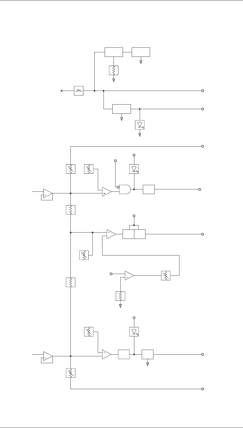
M830P-00 T838/839 Circuit Operation D2.5
Copyright TEL 01/07/00
2.3 Control Circuitry
(Refer to the control section circuit diagram in Section 5.)
Figure 2.3 T838/839 Control Circuitry Block Diagram
+
Comparator
Q129 Q131
FET
Switch
+
+
+
Comparator
FET
Switch
Q117
IC103
RV105
High Reverse Power LED
Low Forward Power LED
Reverse
Power
Meter
Reverse
Power
Alarm
Forward
Power
Meter
Forward
Power
Alarm
+7V
+7V
Tx
Key
IC103
RV101
RV103
+
+
Q137Q135
Q121
+13.8V
Filtered
Integrator
IC105
Control
Supply
-t° R237
NTC
RV109
Power
Control
Shutdown
Power Level
Comparator
IC101 RV113
R154
RV107
R153
Reverse
Power
Sense
Buffer
IC103
Buffer
IC103
Forward
Power
Sense
Ref.
7V
Supply
13.8V
Filtered
L101/L103
13.8V
RV115
Supply LED
IC109
IC107 IC105
Voltage
Regulator
Drive Level Clamp
Forward Power
Alarm
Reverse Power
Alarm
(RF Section)

D2.6 T838/839 Circuit Operation M830P-00
01/07/00 Copyright TEL
2.3.1 Power Control
The DC voltages from the directional coupler representing forward and reflected power
are buffered by the two voltage followers, IC103 pins 1, 2 & 3 and pins 8, 9 & 10. Their
outputs are summed at an integrator (IC105 pins 1, 2 & 3), which drives the series pass
control elements (Q135 & Q137).
Forward and reflected power are summed so that, under high output VSWR, the power
control turns the PA down. This is because the control loop adjusts for the same DC
voltage from the directional coupler that would have been present if there were no
reflected power.
2.3.2 Driver Power Level
The maximum output power of the T838/839 can be limited by placing a ceiling on the
driver output power level using RV115 (accessible through the side cover). For exam-
ple, if RV115 is set for a maximum output power of 50W, the range of adjustment using
RV109 (front panel power adjust) will be 20 to 50W.
Caution: The driver power level clamp (RV115) is factory set to give a maximum
power output of 60W for the T838 and 120W for the T839. The unit may
be damaged if this level is increased.
2.3.3 Thermal Protection
At excessively high temperatures, the output power will automatically reduce to a pre-
set level (set by RV113), thus preventing the PA from overheating.
Ambient temperature within the PA is measured by a thermistor controlled voltage
divider (R168, R237) which applies a voltage to a comparator with hysteresis (IC101
pins 8, 9 & 10). This thermistor is located on the PCB in the low pass filter cavity.
Thermal protection is also provided for each RF power module to prevent the module
itself from overheating. This protection consists of a thermistor controlled voltage
divider (R207, *R215 and R220, R219) which sets a voltage on a comparator with hyster-
esis (IC204 pins 1, 2 & 3 and 5, 6 & 7). These thermistors are located on the module
flanges.
The output current from all comparators is summed into the power control network via
RV113 so that the power level to which the PA must turn down may be set.
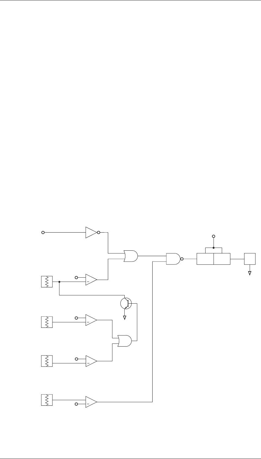
M830P-00 T838/839 Circuit Operation D2.7
Copyright TEL 01/07/00
2.3.4 Forward And Reverse Power Alarms
If forward power drops below, or reverse power rises above, presettable limits, alarms
may be triggered.
The alarm outputs are open drain configuration and are low under normal conditions
(i.e. forward and reverse power levels are normal).
IC103 pins 12, 13 & 14 and pins 5, 6 & 7 form comparators with thresholds adjusted via
RV101 and RV105 respectively. The inputs are from the forward and reverse power sig-
nals from the directional coupler, buffered by IC103 pins 1, 2 & 3 and pins 8, 9 & 10.
Thus, the power levels at which the forward and reverse power alarms are triggered are
defined by RV101 and RV105 respectively.
2.3.5 Forward And Reverse Power Metering
Forward and reverse power signals from the two IC1 buffers are available for metering
purposes. The output currents are adjustable via RV103 (forward power) and RV107
(reverse power).
2.3.6 Fan Control Circuitry
Figure 2.4 T839 Fan Control Logic Diagram
*Q107 *Q109 Fan
Ref +
Ref +
High Temp.
Sense On PCB
Comparator
IC101
R237
High Temp.
Sense On
Module Flange
High Temp.
Sense On
Module Flange
Comparator
IC204
Ref +
Comparator
IC204
*R215
R219
NTC
NTC
Low Temp.
Sense
Comparator
Ref +
IC101
*R116
NTC
NTC
Tx Key
Invert
*Q101 OR
*Q103,
*R106, *R107
OR
Q201
D202, R212,
R214
NAND
*Q103, *Q105,
*R111, *R112 Fan Driver
13.8V
Filtered
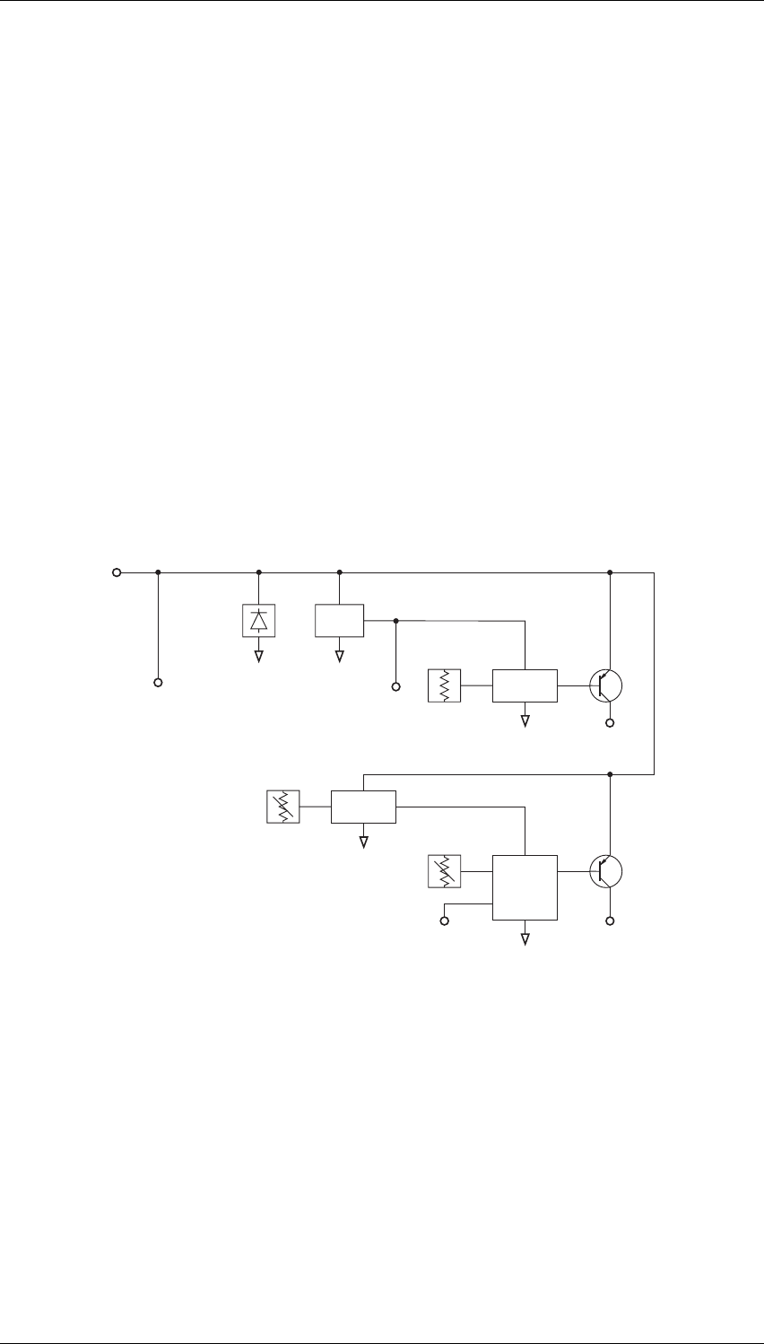
D2.8 T838/839 Circuit Operation M830P-00
01/07/00 Copyright TEL
Comparator IC101 pins 12, 13 & 14 are set to switch at heatsink temperatures greater
than +90°C or RF power module flange temperatures greater than +110°C, and pins 1, 2
& 3 at temperatures less than -10°C.
A logic AND function is applied to the comparator outputs by *Q103 and *Q105,
thereby turning on the fan unconditionally (via *Q107 and *Q109) if the heatsink tem-
perature exceeds +90°C or the module flange temperatures exceed +110°C.
A logic OR function is applied to comparator IC101 pins 12, 13 & 14 and Tx KEY signals,
thereby turning on the fan when the transmitter is keyed and the temperature is
between -10°C and +90°C (or +110°C for the module flanges).
If the temperature drops below -10°C, *Q105 is turned off, preventing *Q103 from acti-
vating the fan.
2.4 Power Supply & Regulator Circuits
(Refer to the control section circuit diagram in Section 5.)
Figure 2.5 T838/839 Power Supply & Regulator Circuitry Block Diagram
The T838/839 are designed to operate off a 10.8-16V DC supply (13.8V nominal). A 7V
supply runs directly off the 13.8V rail, driving the fan control, power control and alarm
circuitry.
A crowbar diode is fitted for protection against connection to a power supply of incor-
rect polarity. It also provides transient overvoltage protection.
Note: A fuse must be fitted in the power supply line for the diode to provide effec-
tive protection.
7V
Reg.
Fan
Control
Power
Clamp
Power
Control
Crowbar
Diode
Temp.
Sense
To Fan
+7V
Clamp
Power
From
Directional
Coupler
Power
Control
Vout
Set
Power
13.8V
Nom.
M830P-00 T838/839 Initial Adjustment D3.1
Copyright TEL 01/07/00
3 T838/839 Initial Adjustment
Caution: This equipment contains CMOS devices which are susceptible to dam-
age from static charges. Refer to Section 1.2 in Part A for more infor-
mation on anti-static procedures when handling these devices.
The following section describes the full adjustment procedure to be carried out before
operating the T838/839.
Note: The T838/839 require no RF tuning or alignment.
Refer to Section 5 where the parts lists, grid reference index and diagrams will provide
detailed information on identifying and locating components. Refer also to Figure 3.2
which shows the location of the main adjustment controls.
The following topics are covered in this section.
Section Title Page
3.1 Test Equipment Required 3.3
3.2 Preliminary Checks 3.3
3.3 Setting The Output Power 3.4
3.4 High Temperature Shutdown Power Level 3.5
3.5 Remote Forward Power Meter Calibration 3.5
3.6 Remote Reverse Power Meter Calibration 3.5
3.7
3.7.1
3.7.2
Setting Alarm Levels
Forward Power
Reverse Power
3.6
3.6
3.6
Figure Title Page
3.1
3.2
T838/839 Test Equipment Set-up
T838/839 Main Adjustment Controls
3.3
3.7

D3.2 T838/839 Initial Adjustment M830P-00
01/07/00 Copyright TEL
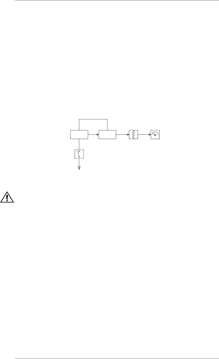
M830P-00 T838/839 Initial Adjustment D3.3
Copyright TEL 01/07/00
3.1 Test Equipment Required
• DC power supply capable of delivering 30A at 13.8V.
• Multimeter or DMM (e.g. Fluke 77).
• RF power meter (e.g. HP 435 series or Bird Wattmeter).
• 150W 30dB attenuator.
• 150W 3dB 50 ohm pad.
• 'BNC' to 'N' type adaptors (e.g. Amphenol, Greenpar).
• Appropriate trimming tools.
Figure 3.1 T838/839 Test Equipment Set-up
Caution: Do not connect attenuators or DC blocks between the T837 and T838/
839 or the cyclic keying circuitry will not function correctly.
3.2 Preliminary Checks
Check for short circuits between the positive rail and earth.
Set up the test equipment as in Figure 3.1.
Connect the T838/839 to a 13.8V DC supply.
Check that the quiescent current is <50mA.
To key the transmitter, earth the key line (D-range 1 [PL100] pin 13) on the exciter.
Check that the power supply is still at 13.8V under load.
Check that the regulated power control supply is approximately 7V.
Note: The output power and alarm levels should be set with the side cover on. If
the cover is removed for other adjustment procedures, make a final check of
the output power and alarm levels with the side cover on.
Exciter PA
Tx Key
RF Power
Meter
Tx Enable
30db
Attenuator
(HP 435)

D3.4 T838/839 Initial Adjustment M830P-00
01/07/00 Copyright TEL
3.3 Setting The Output Power
Caution: If the high temperature shutdown power level has not yet been set or is
unknown, check that the unit does not overheat while setting the out-
put power.
Note 1: You must set up the T838/839 according to the following instructions before
operation in a radio system. Do not use the factory default settings as they
may not suit your operating frequency.
To obtain optimum performance from the T838/839, ensure that the exciter
used in this set-up procedure is the one that will be used with the PA in the
radio system.
Note 2: Cables and connectors can easily cause a power loss of several watts if either
too long or poorly terminated. Always use the shortest possible leads (or
connectors instead of leads) between the T838/839 and power meter set-up.
You will need appropriate extension leads if you wish to carry out the
adjustment procedures with the T838/839 withdrawn from the rack in the
latched position. Alternatively, disconnect and withdraw the T838/839 and
reconnect it behind the rack.
Note 3: The actual power used may be limited by regulatory requirements.
Set the exciter to the required operating frequency.
Connect the exciter output to the PA input via a thru-line wattmeter with a 1W
full scale reading. Special BNC/N leads will be required.
Connect an RF power meter to the PA output connector.
With the exciter not keyed:
• remove the label over the adjustment hole for RV115 (driver power clamp);
• set RV115 to maximum (fully clockwise);
• set RV109 (front panel power control) to maximum (fully clockwise).
Key on the exciter.
Quickly (within 30 seconds) adjust RV115 until the output power is:
T838 - 60W
T839 - 120W.
Adjust RV109 to set the power output to the following levels (or less if required):
T838 - 50W
T839 - 100W.

M830P-00 T838/839 Initial Adjustment D3.5
Copyright TEL 01/07/00
Caution: Do not allow the output power to exceed these levels as this will seri-
ously reduce the reliability of the PA.
Do not use RV115 to set the output power as this will disable the ther-
mal protection circuitry. The power clamp must always be 10W (T838)/
20W (T839) above the set output power.
Replace the label over the adjustment hole for RV115.
3.4 High Temperature Shutdown Power Level
Set RV109 (power control) to the required output power.
Earth pin 9 of IC101 (the via at NTC R237 is convenient).
Adjust RV113 (shutdown power level) for an output power of:
T838 - 16W
T839 - 40W.
Remove the earth from pin 9 of IC101 (or the pad of R237).
To check the operation of the RF power module thermistor(s), place shorting links
across pins 1 & 2 and 2 & 3 of LINK201.
Check that the output power drops to:
T838 - 16W
T839 - 40W.
Remove the shorting links from LINK201.
3.5 Remote Forward Power Meter Calibration
If a remote meter is connected, adjust RV103 (forward power meter calibration)
for the remote reading to agree with the RF power meter reading.
3.6 Remote Reverse Power Meter Calibration
If a remote meter is connected, connect a 50 ohm 3dB pad (with the output open
circuit) to the PA output.
Apply RF drive and Tx key.
Adjust RV107 (reverse power meter calibration) for a quarter of the forward
power reading.

D3.6 T838/839 Initial Adjustment M830P-00
01/07/00 Copyright TEL
3.7 Setting Alarm Levels
Note: If forward and reverse power metering is being used, set up their calibration
(Section 3.5 and Section 3.6) before setting the alarm levels.
3.7.1 Forward Power
Power up the T838/839 and adjust RV109 (front panel power control) so that the
output power is at the alarm level required (e.g. 80W if the T839 normally oper-
ates at 100W).
Adjust RV101 (forward power alarm set) so that the forward power alarm LED
lights.
Check the alarm level setting by adjusting the power up and down and observing
the alarm LED. A few watts hysteresis can be expected.
Readjust RV109 for the normal operating level.
Note: Remote indication is available at pin 3 of D-range 1.
3.7.2 Reverse Power
Power up the T838/839 and adjust RV109 (front panel power control) for the nor-
mal operating power level.
Place a known mismatch of the required value (e.g. 3:1 VSWR) and adjust RV105
(reverse power alarm set) so that the reverse power alarm LED lights.
Example: A VSWR of 3:1 can be simulated by connecting an unterminated 3dB pad
(100W) to the PA output. This will result in a return loss of 6dB.
Note: Remote indication is available at pin 4 of D-range 1.
M830P-00 T838/839 Fault Finding D4.1
Copyright TEL 01/07/00
4 T838/839 Fault Finding
Caution: This equipment contains CMOS devices which are susceptible to dam-
age from static charges. Refer to Section 1.2 in Part A for more infor-
mation on anti-static procedures when handling these devices.
The following test procedures and fault finding flow charts may be used to help locate a
hardware problem, however they are by no means a complete fault finding procedure.
If you still cannot trace the fault after progressing through them in a logical manner,
contact your nearest Tait Dealer or Customer Service Organisation. If necessary, you can
get additional technical help from Customer Support, Radio Systems Division, Tait Elec-
tronics Ltd, Christchurch, New Zealand (full contact details are on page 2).
Refer to Section 5 where the parts lists, grid reference index and diagrams will provide
detailed information on identifying and locating components.
The following topics are covered in this section.
Section Title Page
4.1 Visual Checks 4.3
4.2 DC Checks 4.3
4.3 RF Checks 4.3
4.4
4.4.1
4.4.2
4.4.3
4.4.4
Fault Finding Charts
T838 PA
T839 PA
Power Control
Fan Control Circuitry
4.7
4.7
4.8
4.9
4.10
4.5 Replacing RF Power Modules 4.11
4.6 Removing The PCB From The Heatsink 4.12
Figure Title Page
4.1 Positioning Of Test Leads 4.6

D4.2 T838/839 Fault Finding M830P-00
01/07/00 Copyright TEL

M830P-00 T838/839 Fault Finding D4.3
Copyright TEL 01/07/00
4.1 Visual Checks
Remove the side cover from the T838/839 and inspect the PCB for damaged or
broken components, paying particular attention to the surface mounted devices
(SMDs). Also check for defective solder joints.
Refer to Section 4.5, Section 4.6 and Section 3 of Part A for more details on repair
and replacement of components.
4.2 DC Checks
Check that +13.8V is present on pin 3 of *#IC202 and/or #IC201. Make this meas-
urement when the transmitter is not keyed.
Check that approximately 6-13V is present on pin 2 of *#IC202 and/or #IC201 (the
level is dependent on the setting of RV109).
Check that +13.8V is present at pin 4 of IC103.
Check that approximately +12V is present at pin 8 of IC105 (the level is dependent
on the setting of RV109).
Check that +7.0V is present at the output of regulator IC109.
4.3 RF Checks
The PA Fault Finding Charts (Section 4.4.1 & Section 4.4.2) provide a systematic
approach for locating a fault in the RF circuitry. Use these charts in conjunction with
Figure 4.1, which shows the locations of the 50Ω input and output test points for RF
power modules #IC201 and *#IC202.
Note 1: Use good quality 50Ω coax for the "flying" test leads.
Note 2: Ensure each output is terminated in a 50Ω load of the correct power rating.
For problems with the power control circuitry, refer to the Power Control Fault Finding
Chart (Section 4.4.3).

D4.4 T838/839 Fault Finding M830P-00
01/07/00 Copyright TEL

M830P-00 T838/839 Fault Finding D4.5
Copyright TEL 01/07/00
replace A4 pages D4.5/D4.6 with A3 pages D4.5/D4.6

D4.6 T838/839 Fault Finding M830P-00
01/07/00 Copyright TEL
replace A4 pages D4.5/D4.6 with A3 pages D4.5/D4.6
M830P-00 T838/839 Fault Finding D4.7
Copyright TEL 01/07/00
4.4 Fault Finding Charts
4.4.1 T838 PA
RF circuitry OK.
N
Y
Y
Is RV109
fully clockwise? Rotate RV109
fully clockwise.
Y
Is RV115
fully clockwise? Rotate RV115
fully clockwise.
N
N
Is maximum power >50W
over entire frequency range?*
Earth D-range pin 12 or
connect to exciter key line.
N
Y
*Frequency Ranges
T838-10: 136-156MHz
T838-20: 148-174MHz
Is the drive from the
exciter 600mW-1W? Set drive to
600mW-1W.
Is the output from
#IC201 >60W?
Refer to Figure 4.1.
NCheck #IC201 solder joints.
If joints OK, replace module.
Check components in LPF.
Check output N-type connector
for short circuit or excessive wear.
Replace parts as necessary.
Is maximum power >50W
over entire frequency range?*
N
Return PA to your local
Tait service centre.
Y
Is #IC201 pin 2 >10V?
Is #IC201 pin 3 >13V?
Replace Q135 & Q137,
then check #IC201 pin 2
for short circuit.
Y
Y
N
N
Set RV115 to 60W
(driver power clamp).
Set RV109 to required
output power.
Refer to Section 3.3.
Is the PA keyed?
(D-range pin 12 low)
Y
*Frequency Range
T838-20: 148-174MHz
D4.8 T838/839 Fault Finding M830P-00
01/07/00 Copyright TEL
4.4.2 T839 PA
RF circuitry OK.
N
Y
Y
Is RV109
fully clockwise? Rotate RV109
fully clockwise.
Y
Is RV115
fully clockwise? Rotate RV115
fully clockwise.
Is maximum power >100W
over entire frequency range?*
N
N
Return PA to your local
Tait service centre.
N
Is maximum power >100W
over entire frequency range?*
Y
*Frequency Ranges
T839-10: 136-156MHz
T839-20: 148-174MHz
Replace splitter hybrid.
Check the condition of
splitter hybrid *IC203.
Are there any shorts
on the legs or broken legs?
Y
N
Replace combiner hybrid.
Check the condition of
combiner hybrid *IC205.
Are there any shorts
on the legs or broken legs?
N
Y
Y
N
Is the output from #IC201
and *#IC202 >60W per module
(measured concurrently)?
Refer to Figure 4.1.
Check #IC201/*#IC202 solder joints.
If joints OK, replace module(s).
Check components in LPF.
Check output N-type connector
for short circuit or excessive wear.
Replace parts as necessary.
N
Is *R223 hot to touch
when PA keyed? Y
Set RV115 to 120W
(driver power clamp).
Set RV109 to required
output power.
Refer to Section 3.3.
N
Y
Is the drive from the
exciter 600mW-1W? Set drive to
600mW-1W.
Earth D-range pin 12 or
connect to exciter key line.
Y
NIs the PA keyed?
(D-range pin 12 low)
Is #IC201/*#IC202 pin 2 >10V?
Is #IC201/*#IC202 pin 3 >13V? NReplace Q135 & Q137,
then check #IC201/*#IC202
pin 2 for short circuit.
Y
*Frequency Range
T839-20: 148-174MHz
M830P-00 T838/839 Fault Finding D4.9
Copyright TEL 01/07/00
4.4.3 Power Control
Approximate voltages (@ 174MHz) under normal operating conditions:
Forward & Reverse Power
Measurement
Output Power
50W 100W
forward power at IC103 pin 1
forward power at C261
reverse power at IC103 pin 8
reverse power at C294
2.3V
4.1V
0.6V
0.3V
3.3V
6.0V
0.6V
0.6V
N
Check 12V DC present
on IC105 pin 8.
Check sense voltages
from directional coupler.
Check IC103 pins 1 & 8.
RF Power Level Control Check
Check Q117 & Q121.
Check IC103 pin 14 >12V DC
when forward power low.
Low Forward Power Alarm Check
Y
Y
N
Does high reverse power alarm
LED light when PA operated into
a mismatch of 3:1 or worse?
Check Q129 & Q131.
Check IC103 pin 7 >12V DC
when reverse power high.
High Reverse Power Alarm Check
N
Y
Earth IC101 pin 9.
Check IC103 pin 13 is at 0.6V.
Check IC103 pin 14 goes from
high to low when IC101 pin 9
is earthed. Check Q133.
Y
Over-Temperature Shutdown Check
N
Power control OK.
Using RV109, does output power
adjust over the range:
At high operating temperatures,
does the output power reduce to:
Using RV109, does low forward
power alarm LED light when
output power reduced to:
The following voltage checks are all done with
RV115 (driver power clamp) set to maximum.
When these tests are finished, reset RV115
to 60W (T838) or 120W (T389).
Caution
T838 10-60W
T839 20-120W?
T838 40W
T839 80W?
T838 14W
T839 40W?
Note: A final confirmation of high temperature
shutdown and/or T839 fan activation at
high temperatures can be obtained by
heating the earth pad of R237 to >130°C
with the tip of a soldering iron. Take care
not to damage R237.
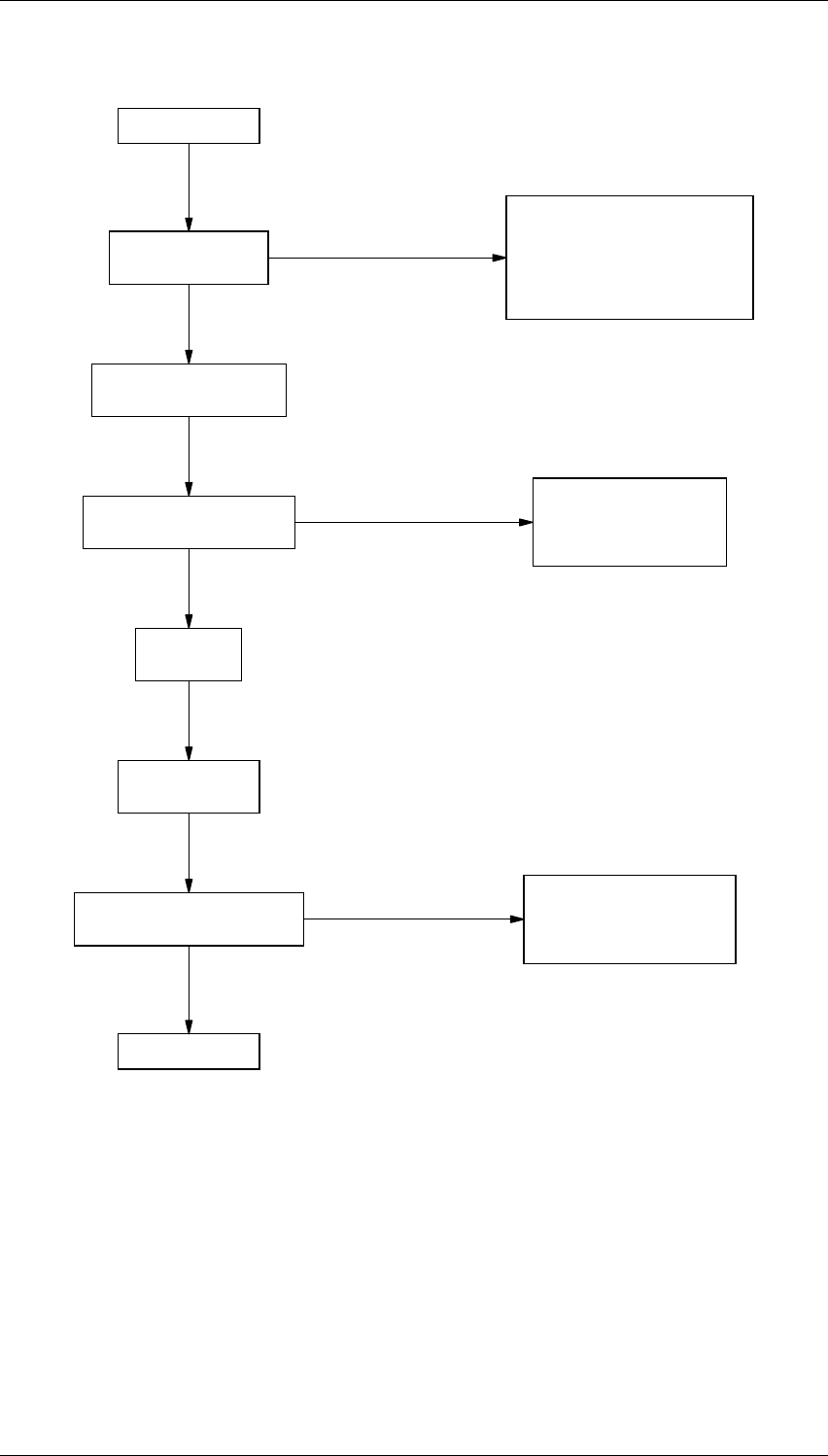
D4.10 T838/839 Fault Finding M830P-00
01/07/00 Copyright TEL
4.4.4 T839 Fan Control Circuitry
Y
Y
Y
Key transmitter.
Does fan run at
room temperature?
Does the low temperature
inhibit circuit stop the fan?
Do not key
transmitter.
Earth IC101 pin 9
(see Section 3.5).
Does high temperature control
circuit activate fan?
Fan control OK.
Earth IC101 pin 9
(see Section 3.5).
Check IC101 pin 14 >11V.
Check *Q105 & *Q103.
N
N
N
Spray "freeze" on *R116
OR short R118.
Check IC101 pin 1 >11V.
Check *Q105 & *Q103.
Spray "freeze" on *R116
OR short R118.
Check *Q103 & *Q105
collector voltages.
Check *Q107 & *Q109.
Check IC101 pin 1 <1V.
Check *Q101.
Check Tx-key is low (at ground).
(see Section 3.4).
(see Section 3.4).

M830P-00 T838/839 Fault Finding D4.11
Copyright TEL 01/07/00
4.5 Replacing RF Power Modules
Caution: Follow these instructions carefully, otherwise the module can fail
because of poor heatsinking or cracked substrates.
Caution:
Do not apply too much heat to the original type of thermistor assembly
as the epoxy used may give off fumes that will cause eye irritation. If
necessary, replace this device as a complete assembly (see note 1 below).
Desolder the module and thermistor1 legs by heating with a soldering iron and
lifting away from the PCB with a screwdriver or thin stainless steel spike.
Undo the module screws and remove the thermistor assembly.
Desolder and remove both earth tags.
Gently lift the module away from the heatsink.
Note: The module may be stuck down quite firmly with heatsink compound. You
may need to carefully prise it away from the heatsink with a small screw-
driver. Keep the heatsink compound clean while the module is detached.
Apply a small amount of heatsink compound (Dow-Corning 340 or equivalent) to
the replacement module mounting surface. Use enough compound to ensure an
even film over the entire mounting surface.
Reposition the module in the correct orientation and ensure it is well pasted to the
heatsink.
Replace the earth tags and thermistor1 assembly in their original positions and
hand-tighten the screws, ensuring the tags and thermistor remain in place. Alter-
nately tighten each screw evenly, finally torquing them down to 56N.cm/5in.lbf.
with an accurate torque driver.
Caution: It is essential that you apply the correct torque to these screws to allow
the module flange to expand and contract under temperature cycling.
Also, do not solder any module legs before torquing down otherwise
the device may be broken.
Solder all module legs to the PCB.
Carefully solder the thermistor leg to the PCB1.
1. Later production PAs are fitted with a different type of thermistor which you
do not need to desolder from the PCB before removing a power module. Refer
to the top side PCB layout diagrams in Sections 5.2 and 5.3 for further details.

D4.12 T838/839 Fault Finding M830P-00
01/07/00 Copyright TEL
4.6 Removing The PCB From The Heatsink
Note: This is a lengthy procedure and should be considered only after all other
checks have been carried out. There are no components on the bottom of the
PCB.
Remove the harmonic filter shield lid.
T839 Only: Desolder the power feed to the fan from the PCB.
Remove the output 50 ohm coaxial connector by unscrewing it from the heatsink
casting and desoldering it from the PCB and harmonic filter shield wall.
Unplug the input 50 ohm coaxial cable from the PCB, unscrew the BNC connector
from the heatsink, and remove the connector and cable.
Desolder the positive and negative power feed wires from the D-range PCB.
Disconnect the ribbon cable from the D-range PCB.
Remove the 2 screws securing the D-range connector and PCB to the heatsink and
withdraw the assembly from the heatsink.
Remove the mounting screws for the TO-220 device(s): Q137 (and *R223 in the
T839).
Remove the screws securing the RF power module(s): #IC201 (and *#IC202 in the
T839).
T839 Only: Remove the four hex nuts and washers from the splitter/com-
biner hybrids (*IC203 and *IC205).
Remove the 11 PCB retaining screws.
Push the three LEDs out of their front panel grommets.
Lift the PCB gently from the heatsink to gain access to the underside of the board.
Note: #IC201, *#IC202 and *R223 may be stuck down with heatsink compound.
You may need to carefully prise them away from the heatsink with a small
screwdriver.
Caution: Keep the heatsink compound clean while the PCB is detached. Any
objects caught in the heatsink compound underneath the module
which prevent effective earthing and/or heatsinking will cause cata-
strophic failure.
Caution: Do not operate the PA with the PCB detached as the heatsink is used
for earthing and heat dissipation.

M830P-00 T838/839 Fault Finding D4.13
Copyright TEL 01/07/00
To replace the PCB, reverse the order of removal, taking care that the wiring is cor-
rectly positioned and not 'pinched'.
Make sure that the heatsink compound has stayed clean, and that the insulating
pad for Q137 is not damaged.
If you have difficulty refitting the LEDs, try pushing the body of the LED back
into the grommet with a thin screwdriver or spike.
Caution: Tighten the splitter/combiner hybrid hex nuts to a torque of 22N.cm/
2in.lbf. Any greater force will damage the devices.
Tighten the RF power module screws to a torque of 56N.cm/5in.lbf.
with an accurate torque driver. Deviating from this figure can cause
the device to fail (refer to Section 4.5).

D4.14 T838/839 Fault Finding M830P-00
01/07/00 Copyright TEL
M830P-00 T838/839 PCB Information D5.1.1
Copyright TEL 01/07/00
5 T838/839 PCB Information
Caution: This equipment contains CMOS devices which are susceptible to damage from
static charges. Refer to Section 1.2 in Part A for more information on anti-static
procedures when handling these devices.
This section provides the following information on the T838 and T839 power amplifiers:
•parts lists
• grid reference indexes
• mechanical assembly drawings
•PCB layouts
• circuit diagrams.
The T838 and T839 share the same basic design and are built on the same PCB. However, in order to
simplify the presentation of the PCB information for each product, we have provided a separate
parts list, grid reference index and set of drawings for both the T838 and T839, even though this has
meant duplicating some information (e.g. grid reference index and circuit diagrams) in each section.
Section Title IPN Page
5.1 Introduction 5.1.3
5.2 T838 Power Amplifier PCB 220-01404-03 5.2.1
5.3 T839 Power Amplifier PCB 220-01404-03 5.3.1

D5.1.2 T838/839 PCB Information M830P-00
01/07/00 Copyright TEL
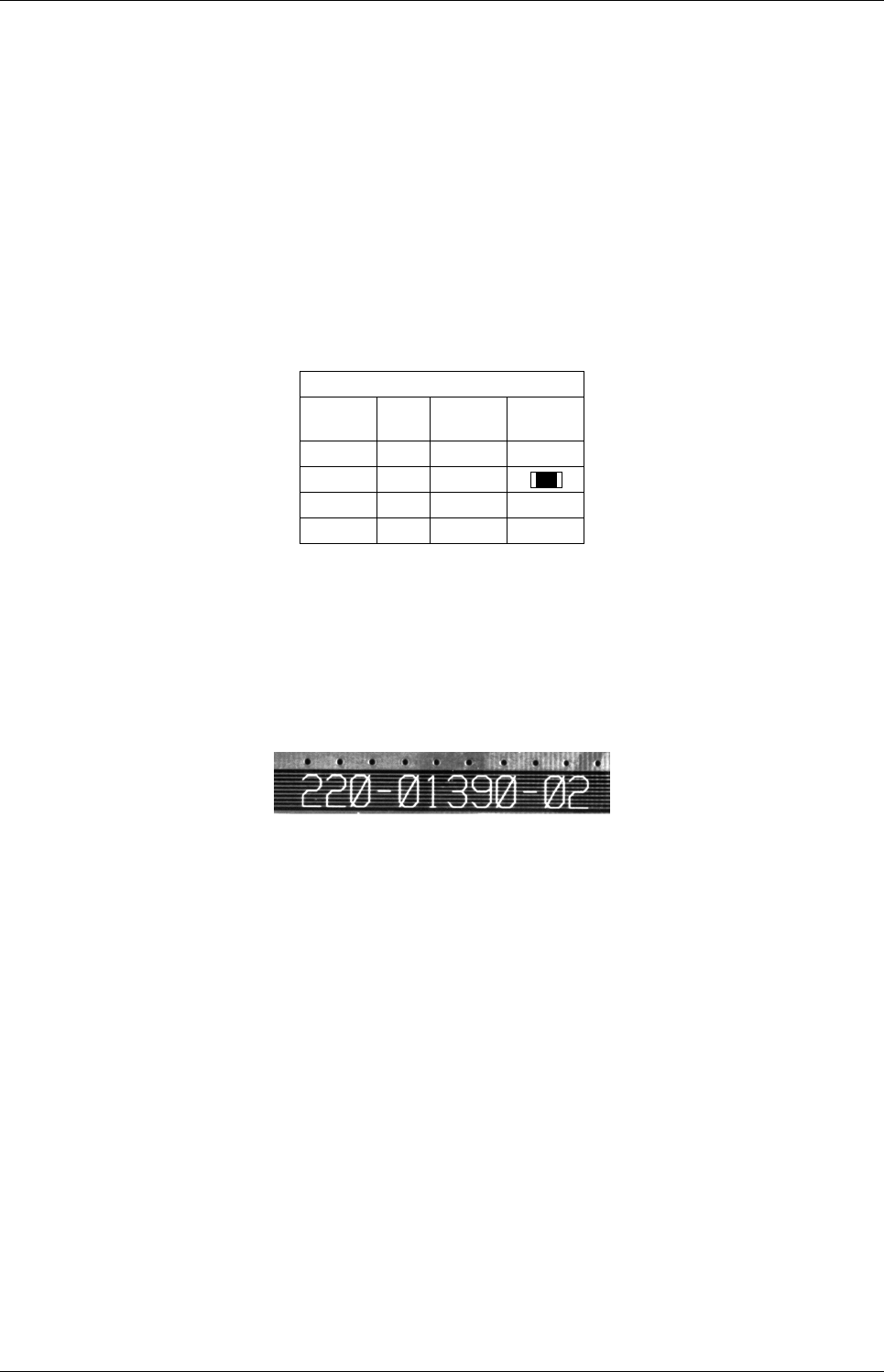
M830P-00 T838/839 PCB Information D5.1.3
Copyright TEL 01/07/00
5.1 Introduction
Product Type Identification
You can identify the PA type by checking the product code printed on a label on the rear of the heat-
sink (product codes are explained in Section 1.3 in this Part of the manual, and Figure 1.1 in Part A
shows typical labels). You can further verify the PA type by checking the placement of an SMD
resistor in the table that is screen printed onto the PCB, similar to the example drawn below. In this
example, the resistor indicates that the product was built as a T830 Series II compatible
T839-20-XXXX.
PCB Identification
All PCBs are identified by a unique 10 digit “internal part number” (IPN), e.g. 220-12345-00, which
is screen printed onto the PCB (usually on the top side), as shown in the example below:
The last 2 digits of this number define the issue status, which starts at 00 and increments through 01,
02, 03, etc. as the PCB is updated. Some issue PCBs never reach full production status and are there-
fore not included in this manual. A letter following the 10 digit IPN has no relevance in identifying
the PCB for service purposes.
Note: It is important that you identify which issue PCB you are working on so that you can
refer to the appropriate set of PCB information.
PRODUCT TYPE
MODEL REV SERIES
I
SERIES
II
T839-10 3A
T839-20 3A
T838-10 3A
T838-20 3A
Note:
The only function of this
resistor is to indicate the
product type. It has no
effect on the circuitry or
operation of the PA.
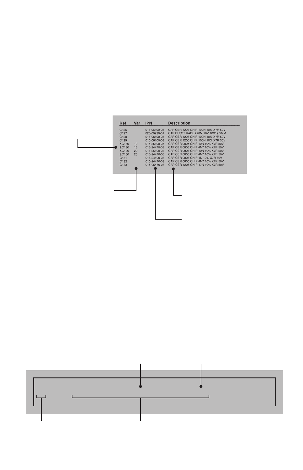
D5.1.4 T838/839 PCB Information M830P-00
01/07/00 Copyright TEL
Parts Lists
The 10 digit numbers (000-00000-00) in this Parts List are “internal part numbers” (IPNs). We can
process your spare parts orders more efficiently and accurately if you quote the IPN and provide a
brief description of the part.
The components listed in this parts list are divided into two main types: those with a circuit refer-
ence (e.g. C2, D1, R121, etc.) and those without (miscellaneous and mechanical).
Those with a circuit reference are grouped in alphabetical order and then in numerical order within
each group. Each component entry comprises three or four columns, as shown below:
The mechanical and miscellaneous section lists the variant and common parts in IPN order.
Parts List Amendments
At the front of the parts list is the Parts List Amendments box (an example of which is shown
below). This box contains a list of component changes which took place after the parts list and dia-
grams in this section were compiled. These changes (e.g. value changes, added/deleted compo-
nents, etc.) are listed by circuit reference in alphanumeric order and supersede the information
given in the parts list or diagrams. Components without circuit references are listed in IPN order.
The number in brackets at the end of each entry refers to the Tait internal Change Order document.
circuit reference -
lists components
in alphanumeric
order
variant column -
indicates that this is
a variant component
which is fitted only to
the product type listed
Internal Part Number -
order the component
b
y
this number
description -
gives a brief description
of the component
Parts List Amendments
R306 Changed from 180Ωto 560Ω(036-13560-00) to increase sensitivity (71003).
circuit reference
or IPN description
of change
IPN of new
component Change Order
number
M830P-00 T838/839 PCB Information D5.1.5
Copyright TEL 01/07/00
Variant Components
A variant component is one that has the same circuit reference but different value or specification in
different product types. Where two products share the same PCB, the term “variant” is also used to
describe components unplaced in one product. Variant components have a character prefix, such as
“&”, “=” or “#”, before the circuit reference (e.g. &R100).
The table below explains the variant prefixes used in T800 Series II products:
Grid Reference Index
This section contains a component grid reference index to help you find components and labelled
pads on the PCB layouts and circuit diagrams. This index lists the components and pads in alpha-
numeric order, along with the appropriate alphanumeric grid references, as shown below:
If the variant prefix is. . . the component will. . .
& change according to channel spacing
= change according to frequency stability
# change according to frequency range
% change or be placed/unplaced for special applications
*be unplaced in one product
(where two products share the same PCB)
circuit diagram
reference
PCB layout
reference
components listed
in alphanumeric order
layer number -
1 = top side layer
2 = bottom side layer
component location
on the layer
sheet number
component location
on the sheet
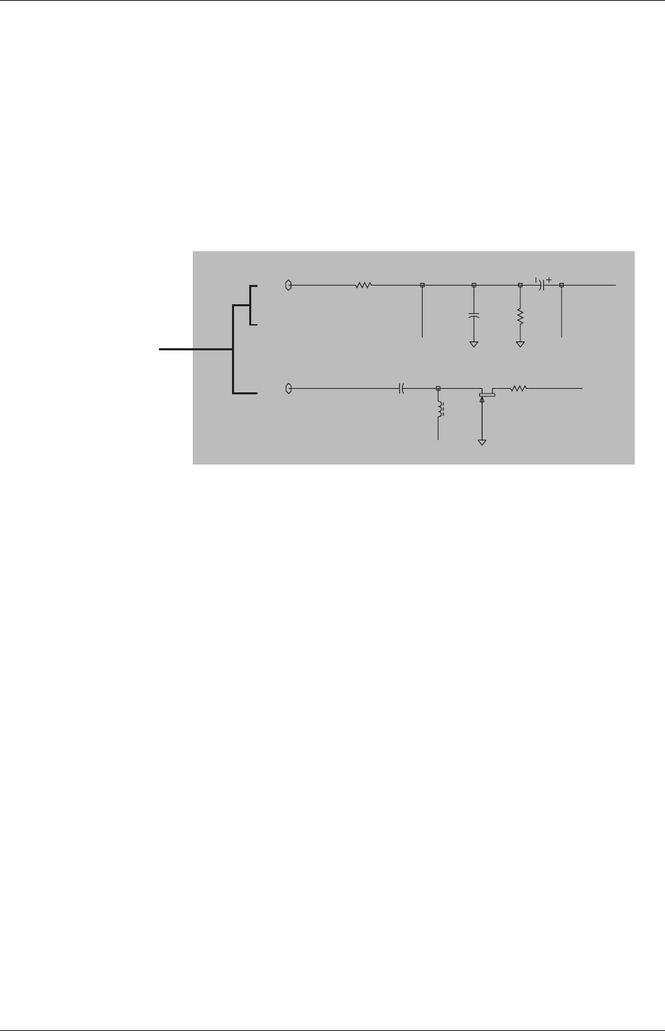
D5.1.6 T838/839 PCB Information M830P-00
01/07/00 Copyright TEL
Using CAD Circuit Diagrams
Reading a CAD circuit diagram is similar to reading a road map, in that both have an alphanumeric
border. The circuit diagrams in this manual use letters to represent the horizontal axis, and num-
bers for the vertical axis. These circuit diagram “grid references” are useful in following a circuit
that is spread over two or more sheets.
When a line representing part of the circuitry is discontinued, a reference will be given at the end of
the line to indicate where the rest of the circuitry is located, as shown below. The first digit refers to
the sheet number and the last two characters refer to the location on that sheet of the continuation of
the circuit (e.g. 1R3).
C301
4N7
R303
12
D
S
G
L310
33U
IF-SIG
4R4
C369
100P
C371
10U
R339
100K
%R338
100
DISCRIMINATOR
1R3
2R9
2R9
8A2
t
hese grid references
s
how where the circuit
is continued

M830P-00 T838 PCB Information D5.2.1
Copyright TEL 01/07/00
5.2 T838 Power Amplifier PCB
This section contains the following information.
IPN Section Page
220-01404-03 Parts List
Mechanical & Miscellaneous Parts
Mechanical Assembly
Grid Reference Index
PCB Layout - Bottom Side
PCB Layout - Top Side
Control Section Circuit Diagram
RF & Thermistor Control Sections Circuit Diagram
5.2.3
5.2.8
5.2.9
5.2.11
5.2.13
5.2.14
5.2.15
5.2.16

D5.2.2 T838 PCB Information M830P-00
01/07/00 Copyright TEL

IPN 220-01404-03
M830P-00 T838 PCB Information D5.2.3
Copyright TEL 01/07/00
T838 Parts List (IPN 220-01404-03)
How To Use This Parts List
The components listed in this parts list are divided into two main types: those with a circuit reference (e.g. C2, D1, R121, etc.) and
those without (miscellaneous and mechanical).
Those with a circuit reference are grouped in alphabetical order and then in numerical order within each group. Each component
entry comprises three or four columns: the circuit reference, variant (if applicable), IPN and description. A number in the variant col-
umn indicates that this is a variant component which is fitted only to the product type listed. Static sensitive devices are indicated by
an (S) at the start of the description column.
The miscellaneous and mechanical section lists the variant and common parts in IPN order. Where possible, a number in the legend
column indicates their position in the mechanical assembly drawing.
The Parts List Amendments box below lists component changes that took place after the parts list and diagrams in this section were
compiled. These changes (e.g. value changes, added/deleted components, etc.) are listed by circuit reference in alphanumeric order
and supersede the information given in the parts list or diagrams. Components without circuit references are listed in IPN order.
Parts List Amendments
D101, D105 Removed from the main PCB and replaced by two 1N4148 diodes (IPN 001-50012-00) placed on the D-range
PCB: one soldered between PL101 pins 5 and 7 (cathode), the other between PL101 pins 6 and 8 (cathode). To
allow external power meters to read zero and still provide meter overvoltage protection (710978).
D113 Changed from MR750 (IPN 001-00011-60) to MR2520L (IPN 001-00012-90) to provide overvoltage transient sup-
pression (750087/88/89/90/91/92).
IC204 Changed from LMC622CM to LM358 (710382).
R123, R158 Changed from 1k resistors (IPN 036-14100-00) to BA592 diodes (IPN 001-10059-20) to allow external power
meters to read zero (710978).
R207 Changed from 47k (IPN 036-15470-10) to 4k7 (IPN 036-14470-10)
R209 Changed from 1k5 (IPN 036-14150-10) to 390Ω (IPN 036-13390-10)
R210 Changed from 4k7 (IPN 036-14470-10) to 390Ω (IPN 036-13390-10)
R213 Changed from 3k9 (IPN 036-14390-00) to 560Ω (IPN 036-13560-00)
R218 Changed from 390Ω (IPN 036-13390-10) to 100Ω (IPN 036-13100-10)
R219 Changed from 100k NTC (IPN 045-06100-05) to 10k NTC (IPN 045-05100-02)
R220 Changed from 47k (IPN 036-15470-10) to 4k7 (IPN 036-14470-10)
R222 Changed from 47k (IPN 036-15470-10) to 4k7 (IPN 036-14470-10)
R224 Changed from 1k5 (IPN 036-14150-10) to 390Ω (IPN 036-13390-10)
R228 Changed from 4k7 (IPN 036-14470-10) to 390Ω (IPN 036-13390-10)
R229 Changed from 56k (IPN 036-15560-10) to 6k8 (IPN 036-14680-10)
349-00020-36 The two M3x8 Torx screws which secure the module into the rack frame have been replaced by M3x8 Pozidriv
screws (IPN 349-00020-55) (750101/2/3/5/6).
100k thermistor assembly
replaced with 10k item;
values of associated compo-
nents changed accordingly
(710394/411/447).

IPN 220-01404-03
D5.2.4 T838 PCB Information M830P-00
01/07/00 Copyright TEL
Parts List Amendments - Continued
This page is provided for entering future amendments to the parts list.

IPN 220-01404-03
M830P-00 T838 PCB Information D5.2.5
Copyright TEL 01/07/00
Ref Var IPN Description Ref Var IPN Description
C129 015-23680-08 CAP CER 0805 680P 10% X7R 50V
C131 015-27100-10 CAP CER 0805 1M+80-20% Y5V 16V
C132 015-24100-08 CAP CER 0805 1N 10% X7R 50V
C133 015-23680-08 CAP CER 0805 680P 10% X7R 50V
C137 015-23680-08 CAP CER 0805 680P 10% X7R 50V
C138 015-24470-08 CAP CER 0805 4N7 10% X7R 50V
C139 015-23680-08 CAP CER 0805 680P 10% X7R 50V
C141 014-07100-02 CAP TANT CHIP 1U0 3.2 X 1.6MM
C143 015-23680-08 CAP CER 0805 680P 10% X7R 50V
C145 015-23680-08 CAP CER 0805 680P 10% X7R 50V
C147 015-24470-08 CAP CER 0805 4N7 10% X7R 50V
C149 015-23680-08 CAP CER 0805 680P 10% X7R 50V
C151 015-23680-08 CAP CER 0805 680P 10% X7R 50V
C153 015-23680-08 CAP CER 0805 680P 10% X7R 50V
C155 015-25100-08 CAP CER 0805 10N 10% X7R 50V
C159 015-23680-08 CAP CER 0805 680P 10% X7R 50V
C161 015-23680-08 CAP CER 0805 680P 10% X7R 50V
C162 015-23680-08 CAP CER 0805 680P 10% X7R 50V
C164 015-24470-08 CAP CER 0805 4N7 10% X7R 50V
C165 015-23680-08 CAP CER 0805 680P 10% X7R 50V
C167 015-24100-08 CAP CER 0805 1N 10% X7R 50V
C169 014-07470-03 L) CAP TANT SMD 4U7 35V 20%
C171 015-24470-08 CAP CER 0805 4N7 10% X7R 50V
C173 015-23680-08 CAP CER 0805 680P 10% X7R 50V
C174 015-23680-08 CAP CER 0805 680P 10% X7R 50V
C176 015-06100-08 CAP CER 1206 100N 10% X7R 50V
C178 015-25100-08 CAP CER 0805 10N 10% X7R 50V
C179 015-06150-08 CAP CER1206150N10% X7R25VW 25V
C180 015-23680-08 CAP CER 0805 680P 10% X7R 50V
C181 015-23100-01 CAP CER 0805 100P 5% NPO 50V
C182 015-24470-08 CAP CER 0805 4N7 10% X7R 50V
C184 015-25100-08 CAP CER 0805 10N 10% X7R 50V
C185 015-23680-08 CAP CER 0805 680P 10% X7R 50V
C186 015-23680-08 CAP CER 0805 680P 10% X7R 50V
C187 015-06100-08 CAP CER 1206 100N 10% X7R 50V
C188 014-08100-00 CAP TANT CHIP 10M 16VW +-20%
C189 015-25100-08 CAP CER 0805 10N 10% X7R 50V
C190 015-23680-08 CAP CER 0805 680P 10% X7R 50V
C192 015-06100-08 CAP CER 1206 100N 10% X7R 50V
C193 015-06100-08 CAP CER 1206 100N 10% X7R 50V
C195 014-08100-00 CAP TANT CHIP 10M 16VW +-20%
C201 014-07470-03 L) CAP TANT SMD 4U7 35V 20%
*C203 015-03680-06 CAP CER 1210 680P NPO200VGRM42
*C204 015-03680-06 CAP CER 1210 680P NPO200VGRM42
C205 015-06100-08 CAP CER 1206 100N 10% X7R 50V
*C206 015-03680-06 CAP CER 1210 680P NPO200VGRM42
C207 015-06100-08 CAP CER 1206 100N 10% X7R 50V
C215 015-23680-08 CAP CER 0805 680P 10% X7R 50V
C216 015-24470-08 CAP CER 0805 4N7 10% X7R 50V
C218 015-23680-08 CAP CER 0805 680P 10% X7R 50V
C220 015-23680-08 CAP CER 0805 680P 10% X7R 50V
C221 015-06100-08 CAP CER 1206 100N 10% X7R 50V
C222 015-24470-08 CAP CER 0805 4N7 10% X7R 50V
C223 015-24100-08 CAP CER 0805 1N 10% X7R 50V
C224 015-23680-08 CAP CER 0805 680P 10% X7R 50V
C225 015-03680-06 CAP CER 1210 680P NPO200VGRM42
C226 015-23680-08 CAP CER 0805 680P 10% X7R 50V
C227 015-03680-06 CAP CER 1210 680P NPO200VGRM42
C229 015-03680-03 CAP CER 680P 5% NPO100V GRH111
C259 015-23680-08 CAP CER 0805 680P 10% X7R 50V
C261 015-24470-08 CAP CER 0805 4N7 10% X7R 50V
C268 029-02220-02 CAP MICA 5 CASE 22P 5%
C270 029-02560-03 CAP MICA 10 CASE 56P 2%
C271 029-02470-03 CAP MICA 10 CASE 47P 2%
C272 029-02560-03 CAP MICA 10 CASE 56P 2%
C273 029-02220-02 CAP MICA 5 CASE 22P 5%
C294 015-23680-08 CAP CER 0805 680P 10% X7R 50V
C295 015-24470-08 CAP CER 0805 4N7 10% X7R 50V
C297 015-23680-08 CAP CER 0805 680P 10% X7R 50V
C298 015-24470-08 CAP CER 0805 4N7 10% X7R 50V
D101 001-10000-70 (S) DIODE SMD BAV70 D-SW SOT23
D103 008-00013-32 (S) LED 3 RED LO CURRENT NO MTG
D105 001-10000-70 (S) DIODE SMD BAV70 D-SW SOT23
D107 008-00013-35 (S) LED 3 GRN LO CURRENT NO MTG
D109 008-00013-32 (S) LED 3 RED LO CURRENT NO MTG
D111 001-10000-70 (S) DIODE SMD BAV70 D-SW SOT23
D113 001-00011-60 (S) DIODE SR2607 -- USE MR750
D201 001-00013-45 (S) DIODE SCHTTKY 1SS97/2
D202 001-10000-70 (S) DIODE SMD BAV70 D-SW SOT23
D203 001-00013-45 (S) DIODE SCHTTKY 1SS97/2
IC101 002-10003-24 (S) IC SMD 324 4X O-AMP SO14
IC103 002-10003-24 (S) IC SMD 324 4X O-AMP SO14
IC105 002-10003-58 (S) IC SMD LM358 DUAL O-AMP
IC107 002-10003-17 (S) IC LM317L REG S0-8 100MA
IC109 002-10003-17 (S) IC LM317L REG S0-8 100MA
#IC201 10 004-00687-02 MODULE M68702L 135-160MHZ 60W
#IC201 20 004-00687-03 MODULE M68702H 150-174MHZ 60W
IC204 002-10006-62 (S)IC SMD LMC662CM 2X O-AMP
L101 065-10004-20 BEAD FE SMD CBD 4.6/3/3-4S2
L103 065-10004-20 BEAD FE SMD CBD 4.6/3/3-4S2
L105 065-10004-20 BEAD FE SMD CBD 4.6/3/3-4S2
*L201 056-10330-02 (L) IND SMD 330NH
L203 065-10004-20 BEAD FE SMD CBD 4.6/3/3-4S2
L206 056-14150-02 (L) IND SMD 1.5UH
L208 056-14150-02 (L) IND SMD 1.5UH
L215 052-08340-40 COIL A/W 4T/4.0MM SMD 0.8MM
L217 052-08340-40 COIL A/W 4T/4.0MM SMD 0.8MM
L233 056-10330-02 (L) IND SMD 330NH
L239 056-10330-02 (L) IND SMD 330NH
L241 052-08360-20 COIL A/W 2T/6.0MM SMD 0.8MM
L243 052-08340-20 COIL A/W 2T/4.0MM SMD 0.8MM
L245 052-08345-10 COIL A/W 1T/4.5MM SMD 0.8MM
L247 052-08340-20 COIL A/W 2T/4.0MM SMD 0.8MM
L248 052-08345-10 COIL A/W 1T/4.5MM SMD 0.8MM
L249 052-08360-20 COIL A/W 2T/6.0MM SMD 0.8MM
L264 056-10330-02 (L) IND SMD 330NH
LINK1 240-00020-68 HEADER 2W PCB MTG STD
LINK2 036-10000-00 RES M/F 0805 ZERO OHM
LINK201 240-00020-59 HEADER 3 W 1 R PCB MTG
PL101 240-00010-55 PLUG 15 W D RANGE W/W PNL MT
Q111 000-10008-57 (S) XSTR SMD BCW70 PNP SOT23 SS
Q113 000-10008-48 (S) XSTR SMD BCW60 NPN SOT23 SS
Q115 000-10008-57 (S) XSTR SMD BCW70 PNP SOT23 SS
Q117 000-10008-17 (S) XSTR SMD BC817-25 NPN SOT23
Q119 000-10008-48 (S) XSTR SMD BCW60 NPN SOT23 SS
Q121 000-10017-00 LS) XSTR SMD BF170LT1 SOT23
Q123 000-10008-57 (S) XSTR SMD BCW70 PNP SOT23 SS
Q125 000-10008-57 (S) XSTR SMD BCW70 PNP SOT23 SS
Q127 000-10008-57 (S) XSTR SMD BCW70 PNP SOT23 SS
Q129 000-10008-17 (S) XSTR SMD BC817-25 NPN SOT23
Q131 000-10017-00 LS) XSTR SMD BF170LT1 SOT23
Q133 000-10008-48 (S) XSTR SMD BCW60 NPN SOT23 SS
Q135 000-10008-17 (S) XSTR SMD BC817-25 NPN SOT23
Q136 000-10008-17 (S) XSTR SMD BC817-25 NPN SOT23
Q137 000-00030-95 (S) XSTR 2N6107 PNP TO220 AF
Q201 000-10008-48 (S) XSTR SMD BCW60 NPN SOT23 SS
R101 036-14100-00 RES M/F 0805 1K 5%
R103 036-15330-00 RES M/F 0805 33K 5%
R104 036-16470-00 RES M/F 0805 470K 5%
R117 036-16220-00 RES M/F 0805 220K 5%
R118 036-15270-00 RES M/F 0805 27K 5%
R119 036-16470-00 RES M/F 0805 470K 5%
R123 036-14100-00 RES M/F 0805 1K 5%
R124 036-16100-00 RES M/F 0805 100K 5%
R125 036-15100-00 RES M/F 0805 10K 5%
R126 036-14100-00 RES M/F 0805 1K 5%
R127 036-15100-00 RES M/F 0805 10K 5%
R128 036-15220-00 RES M/F 0805 22K 5%
R129 036-17100-00 RES M/F 0805 1M 5%
R130 036-14220-00 RES M/F 0805 2K2 5%
R131 036-16180-00 RES M/F 0805 180K 5%
R132 036-14100-00 RES M/F 0805 1K 5%
R133 036-15100-00 RES M/F 0805 10K 5%
R134 036-13470-00 RES M/F 0805 470E 5%
R135 036-13680-00 RES M/F 0805 680E 5%
R136 036-15100-00 RES M/F 0805 10K 5%
R137 036-13470-00 RES M/F 0805 470E 5%
R138 036-15100-00 RES M/F 0805 10K 5%
R141 036-15100-00 RES M/F 0805 10K 5%
R142 036-15100-00 RES M/F 0805 10K 5%
R143 036-15100-00 RES M/F 0805 10K 5%
R144 036-15820-00 RES M/F 0805 82K 5%
R145 036-15470-00 RES M/F 0805 47K 5%
R146 036-14180-00 RES M/F 0805 1K8 5%
R148 036-14820-00 RES M/F 0805 8K2 5%
R149 036-13470-00 RES M/F 0805 470E 5%
R150 036-12220-00 RES M/F 0805 22E 5%
R151 036-15100-00 RES M/F 0805 10K 5%
R152 036-15100-00 RES M/F 0805 10K 5%
R153 036-14680-00 RES M/F 0805 6K8 5%
R154 036-14680-00 RES M/F 0805 6K8 5%
R155 036-13220-00 RES M/F 0805 220E 5%
R156 036-13100-00 RES M/F 0805 100E 5%
Note: The T838 and T839 share the same basic design and
are built on the same PCB. While most components in
this design are common to both products, there are a
number of components that are placed in only one prod-
uct.
Because the circuit diagrams for this design cover both
products, we have indicated on the diagrams those
components which are placed only in the T838 by
enclosing them in a labelled box. The circuit reference
for each of these components is also prefixed with the
“*”character.
The “*” character is used in this parts list to indicate
components used only in the T838.

IPN 220-01404-03
D5.2.6 T838 PCB Information M830P-00
01/07/00 Copyright TEL
Ref Var IPN Description Ref Var IPN Description
R157 036-12220-00 RES M/F 0805 22E 5%
R158 036-14100-00 RES M/F 0805 1K 5%
R159 036-15100-00 RES M/F 0805 10K 5%
R160 036-14470-00 RES M/F 0805 4K7 5%
R161 036-14100-00 RES M/F 0805 1K 5%
R162 036-17100-00 RES M/F 0805 1M 5%
R163 036-13680-00 RES M/F 0805 680E 5%
R164 036-14220-00 RES M/F 0805 2K2 5%
R165 036-14100-00 RES M/F 0805 1K 5%
R166 036-13680-00 RES M/F 0805 680E 5%
R168 036-15100-10 RES M/F 0805 10K 1%
R169 036-14100-00 RES M/F 0805 1K 5%
R170 036-14100-00 RES M/F 0805 1K 5%
R171 036-14100-00 RES M/F 0805 1K 5%
R172 036-15100-10 RES M/F 0805 10K 1%
R173 036-13470-00 RES M/F 0805 470E 5%
R174 036-13220-00 RES M/F 0805 220E 5%
R175 036-16220-00 RES M/F 0805 220K 5%
R176 036-15100-00 RES M/F 0805 10K 5%
R177 036-14470-00 RES M/F 0805 4K7 5%
R178 036-16100-00 RES M/F 0805 100K 5%
R179 036-15100-00 RES M/F 0805 10K 5%
R180 036-16150-00 RES M/F 0805 150K 5%
R181 036-14560-00 RES M/F 0805 5K6 5%
R182 036-16100-00 RES M/F 0805 100K 5%
R183 036-14470-00 RES M/F 0805 4K7 5%
R184 036-14100-00 RES M/F 0805 1K 5%
R185 036-03100-02 RES 100E 1206 200V 250MW RC01
R186 036-13100-00 RES M/F 0805 100E 5%
R187 036-03150-03 RES 1218 PWR CHIP 150E 20% 1W
R188 036-13220-00 RES M/F 0805 220E 5%
R189 036-12100-00 RES M/F 0805 10E 5%
R190 036-12220-00 RES M/F 0805 22E 5%
R191 036-14100-10 RES M/F 0805 CHIP 1K 1%
R192 036-13220-10 RES 0805 220E 1%
R193 036-12100-00 RES M/F 0805 10E 5%
R194 036-03220-03 RES 1218 PWR CHIP 220E 20% 1W
R195 036-14220-00 RES M/F 0805 2K2 5%
R196 036-13100-00 RES M/F 0805 100E 5%
R197 036-10000-00 RES M/F 0805 ZERO OHM
*R201 036-03330-03 L) RES 1218 PWR 330E 20% 1W
*R202 036-02100-03 L) RES 1218 PWR 10E 20% 1W
R203 036-02100-02 RES 10E 1206 200V 250MW RC01
*R204 036-03330-03 L) RES 1218 PWR 330E 20% 1W
R205 036-02100-02 RES 10E 1206 200V 250MW RC01
R207 036-15470-10 RES M/F 0805 47K 1%
R209 036-14150-10 RES MF 0805 CHIP 1K5 1%
R210 036-14470-10 RES M/F 0805 CHIP 4K7 1%
R212 036-15100-00 RES M/F 0805 10K 5%
R213 036-14390-00 RES M/F 0805 3K9 5%
R214 036-14470-00 RES M/F 0805 4K7 5%
R218 036-13390-10 RES MF 0805 CHIP 390E 1%
R219 available as sub-assembly only - refer to
(045-06100-05) in the mechanical parts list
R220 036-15470-10 RES M/F 0805 47K 1%
R222 036-15470-10 RES M/F 0805 47K 1%
R224 036-14150-10 RES MF 0805 CHIP 1K5 1%
R225 030-03120-00 RES FILM 120E 5% 0.25W 7X2.5
R228 036-14470-10 RES M/F 0805 CHIP 4K7 1%
R229 036-15560-10 RES MF 0805 CHIP 56K 1%
R231 030-03120-00 RES FILM 120E 5% 0.25W 7X2.5
R237 045-04470-00 RES NTC SMD 4K7 5% 20MW
RV101 042-04500-05 RES PRESET SMD 5K CER 4MM SQ
RV103 042-05500-05 RES PRESET SMD 50K CER 4MM SQ
RV105 042-04500-05 RES PRESET SMD 5K CER 4MM SQ
RV107 042-05500-05 RES PRESET SMD 50K CER 4MM SQ
RV109 044-04200-03 RES PRE 2K 10 TURN PNL MTG
RV113 042-06500-05 RES PRESET SMD 500K CER 4MM SQ
RV115 042-04220-05 RES PRESET SMD 2K CER 4MM SQ
SK101 240-10000-05 CONN SMD SKT 8W 2R M-MATCH
SK103 240-10000-05 CONN SMD SKT 8W 2R M-MATCH
*SK203 240-02100-44 SKT COAX MINI JACK PCB MT ANG.
16

IPN 220-01404-03
M830P-00 T838 PCB Information D5.2.7
Copyright TEL 01/07/00

IPN 220-01404-03
D5.2.8 T838 PCB Information M830P-00
01/07/00 Copyright TEL
IPN Legend Description IPN Legend Description
T838 Mechanical & Miscellaneous Parts (220-01404-03)
000-00030-95 9 Q137
004-00687-02/3 14 #IC201
012-04150-01 22 CAP CER F/THRU 1N5 NO LEAD
045-06100-05 16 ASSY 100K NTC FOR MODULE
R219
051-00006-02 SOLDER SPRING 1.3MM A4M1877
Support for front panel LED solder joints.
051-00641-01 3 COAX SEMI-RIG N-TYPE EXTN
051-00642-01 28 COAX SEMI-RIG N-TYPE EXTN
065-00010-13 21 BEAD FER 7D 1.9X0.9X3.8
201-00030-02 WIRE T/C 7/0.2 PVC RED
Front panel LEDs.
201-00030-10 WIRE T/C 7/0.2 PVC BLACK
Front panel LEDs.
201-00050-25 AUTO 154 RED 41/0.3 PVC
DC+ from D-range PCB.
201-00050-26 AUTO 154 BLACK 41/0.3 PVC
DC- from D-range PCB.
206-00010-11 COAX 50 OHM RG316-U PTFE
Coax from BNC connector to *SK203.
219-02591-00 18 LOOM RIBBON 8 WAY FOR PA
219-02592-00 CABLE ASSY RG223/U N TO BNC
Exciter/PA connecting cable.
220-01402-02 2 PCB T838/9 TEFLON DIRNL COUPLER
220-01404-03 1 PCB T838/9 PA MODULE DESIGN
240-00010-55 20 PLUG 15 W D RANGE W/W PNL MT
PL101
240-00100-43 PLG COAX MINI PIN CRIMP 1.5D
Coax from BNC connector to *SK203.
240-02010-54 SKT 15W DRANGE PNL MTG 125 C
Matching socket for D-range plug PL101.
240-02100-06 27 SKT COAX N TYPE PNL MTG OP-TER
240-02100-17 29 SKT COAX BNC PNL JAC CRP RG316
240-04020-62 SKT 2 W RECEP SHORTING LINK
LINK1
240-06010-14 CLAMP LATCHING 15 W D RANGE
Cover for D-range socket.
240-06010-15 25 BLOCK LATCHING 15W D RANGE
240-06010-44 26 HOOD CONN UHF & N-TYPE
303-23120-00 30 COVER A3M2288 HOLE BLANKING
303-23146-00 38 COVER SIDE T838/9PA
308-01007-01 35 HANDLE BASE STATION SERIES II
308-13122-02 6 HEATSINK T838/9 PA COMPLETE
316-06617-00 32 PNL PA NO INP DRV SER II SNGL
319-01152-00 19 SHIELD A3M2250 F/THRU MTG
319-01190-01 4 SHIELD WALL HARM. FILTER
319-01201-00 31 SHIELD LID HARM. FILTER
319-01202-00 5 SHIELD PA CONTROL CIRCUIT
319-30064-00 13 SPACER HSINK RF MODULE
345-00040-16 23 SCRW M3X20MM P/POZ ST BZ
349-00010-59 17 SCRW 6-32 X 3/8 P/PH T/T ZP
349-00020-07 7 SCRW 4-40 X 5/16 P/POZ T/T BLK
349-00020-09 12 SCRW T/T 4-40X3/8 IN P/POZ BLK
349-00020-36 37 LIM)SCREW TT M3X8m PANTORX BLK
352-00010-29 36 NUT M4 NYLOC HEX
353-00010-10 11 WSHR M3 FLAT 7MMX0.6MM ST BZ
356-00010-03 24 TAG SOLDER 3MM LONG M614/3.2
356-00010-05 15 TAG SOLDER 4MM LONG M6144/4.2
360-00010-41 34 BUSH SHORTY BLK
362-00010-07 8 GASKET SIL INSULATING TO-220
362-00010-13 10 BUSH INSULATING 1.1MM TOP HAT
362-00010-33 33 GROMMET LED MTG 3MM
365-00100-20 LABEL WHITE S/A 28X11MM
365-01391-01 LABEL 30X10.8 T/MARK VOID
365-01538-00 LABEL WARNING 60W/PWR CLAMP
369-00010-14 TIE CABLE NYLON 100X2.6MM
399-00010-56 BAG PLASTIC 200X250MM
400-00020-07 SLEEVING 2MM SIL RUBBER
410-00010-43 PKG T296 AMPAC REF 73-46

IPN 220-01404-03
M830P-00 T838 PCB Information D5.2.9
Copyright TEL 01/07/00
replace A4 pages D5.2.9/D5.2.10 with A3 pages D5.2.9/D5.2.10

IPN 220-01404-03
D5.2.10 T838 PCB Information M830P-00
01/07/00 Copyright TEL
replace A4 pages D5.2.9/D5.2.10 with A3 pages D5.2.9/D5.2.10

IPN 220-01404-03
M830P-00 T838 PCB Information D5.2.11
Copyright TEL 01/07/00
Device PCB Circuit Device PCB CircuitDevice PCB Circuit Device PCB Circuit
T838 Grid Reference Index (IPN 220-01404-03)
How To Use This Grid Reference Index
The first digit in the PCB layout reference is a "1" or "2", indicating the top or bottom side layout respectively, and the last two charac-
ters give the location of the component on that diagram.
The first digit in the circuit diagram reference is the sheet number, and the last two characters give the location of the component on
that sheet.
*C101 1:E4 1-B8
*C103 1:E4 1-B9
*C105 1:B3 1-D8
*C107 1:B3 1-D9
*C109 1:B3 1-D8
*C111 1:C4 1-D8
*C113 1:B5 1-F8
*C115 1:B5 1-F8
*C117 1:B5 1-F9
*C119 1:B5 1-G8
*C121 1:D4 1-B6
*C123 1:D4 1-B6
*C124 1:E3 1-C6
*C125 1:C4 1-D7
*C127 1:C4 1-D6
C129 1:B3 1-H5
C131 1:B3 1-J6
C132 1:A3 1-K7
C133 1:B4 1-K8
C137 1:B2 1-K8
C138 1:B2 1-L8
C139 1:B4 1-M6
C141 1:B3 1-M8
C143 1:E3 1-E7
C145 1:E3 1-F7
C147 1:D3 1-F6
C149 1:D3 1-F7
C151 1:C5 1-D5
C153 1:B5 1-D3
C155 1:D3 1-G3
C159 1:B3 1-H2
C161 1:B4 1-K4
C162 1:B3 1-L4
C164 1:B3 1-L4
C165 1:B3 1-M4
C167 1:K3 1-P3
C169 1:K3 1-P3
C171 1:K3 1-Q3
C173 1:D4 1-B0
C174 1:E4 1-B0
C176 1:D4 1-E0
C178 1:C4 1-F0
C179 1:D3 1-G2
C180 1:E2 1-H0
C181 1:D3 1-G0
C182 1:D3 1-H1
C184 1:D4 1-G0
C185 1:D2 1-J1
C186 1:E2 1-J0
C187 1:D3 1-K1
C188 1:C2 1-L1
C189 1:C3 1-M1
C190 1:C3 1-N1
C192 1:B2 1-N1
C193 1:B2 1-P1
C195 1:C2 1-Q1
C201 1:J7 2-L5
*C202 1:H3 2-B8
*C203 1:P7 2-C1
*C204 1:M6 2-E1
C205 1:L7 2-I5
*C206 1:P6 2-C1
C207 1:K7 2-K5
*C208 1:H3 2-C8
*C209 1:C5 2-D8
*C210 1:C5 2-E8
*C212 1:D5 2-G9
*C213 1:D4 2-H9
C215 1:D5 2-J8
C216 1:H6 2-B6
*C217 1:P3 2-E3
C218 1:H5 2-C6
*C219 1:P2 2-E3
C220 1:E5 2-D6
C221 1:E5 2-N8
C222 1:E5 2-E6
C223 1:D5 2-G7
C224 1:D5 2-M8
C225 1:L6 2-I4
C226 1:D4 2-H7
C227 1:K6 2-J4
C229 1:H6 2-K4
*C230 1:L4 2-I2
*C231 1:L4 2-I1
*C232 1:K4 2-J1
*C233 1:K4 2-K2
*C234 1:J4 2-L1
*C240 1:H4 2-K1
C259 1:F7 2-Q3
C261 1:F6 2-Q4
C268 1:E6 2-S2
C270 1:D6 2-T2
C271 1:C6 2-T2
C272 1:B6 2-U2
C273 1:B6 2-V2
C294 1:D6 2-R1
C295 1:D6 2-R1
C297 1:C5 2-L8
C298 1:C6 2-L8
D101 1:B3 1-H5
D101 1:B3 1-G5
D103 1:P7 1-K9
D105 1:C2 1-J2
D105 1:C2 1-J2
D107 1:P7 1-K5
D109 1:P6 1-L5
D111 1:C2 1-M1
D111 1:C2 1-M1
D113 1:F7 1-Q2
D201 1:F6 2-Q3
D202 1:D4 2-I8
D202 1:D4 2-I8
D203 1:E6 2-R2
IC101 1:D4 1-C6
IC101 1:D4 1-G0
IC101 1:D4 1-B8
IC101 1:D4 1-C0
IC101 1:D4 1-N0
IC103 1:C4 1-D4
IC103 1:C4 1-J8
IC103 1:C4 1-F0
IC103 1:C4 1-J5
IC103 1:C4 1-E3
IC105 1:D3 1-M0
IC105 1:D3 1-P0
IC105 1:D3 1-G2
IC107 1:D3 1-K1
IC109 1:B2 1-N1
#IC201 1:K7 2-I4
*#IC202 1:K4 2-I1
*IC203 1:N5 2-F2
IC204 1:D5 2-H7
IC204 1:D5 2-H8
IC204 1:D5 2-N8
*IC205 1:G5 2-P2
L101 1:K3 1-P3
L103 1:K2 1-Q3
L105 1:E2 1-K0
*L201 1:P7 2-C1
*L202 1:H3 2-B8
L203 1:L7 2-I6
*L204 1:C5 2-D8
L206 1:H5 2-B7
L208 1:E5 2-D7
*L211 1:P2 2-D3
L215 1:L7 2-I5
L217 1:J7 2-K5
*L223 1:J4 2-K2
*L230 1:L4 2-I3
*L231 1:L4 2-I2
L233 1:F6 2-Q3
*L236 1:H6 2-M2
L239 1:E5 2-R2
L241 1:D6 2-S3
L243 1:C6 2-T3
L245 1:C7 2-T2
L247 1:C6 2-U3
L248 1:D7 2-U2
L249 1:B6 2-V3
L264 1:C6 2-L8
LINK1 1:D3 1-L0
LINK2 1:P6 1-D1
LINK201 1:D5 2-F8
P101 1:A5 1-R9
P103 1:K3 1-R0
P105 1:K2 1-R0
P201 1:B6 2-V3
PL101 1:L3 1-C2
*Q101 1:C3 1-C9
*Q103 1:B3 1-E8
*Q105 1:C4 1-D7
*Q107 1:B5 1-F8
*Q109 1:A5 1-G9
Q111 1:A3 1-J7
Q113 1:A3 1-K6
Q115 1:A3 1-L7
Q117 1:B4 1-K8
Q119 1:B4 1-L6
Q121 1:B3 1-L8
Q123 1:E3 1-E7
Q125 1:E3 1-F7
Q127 1:D3 1-G7
Q129 1:B4 1-L4
Q131 1:B3 1-M5
Q133 1:D4 1-D0
Q135 1:E2 1-H0
Q136 1:E3 1-H0
Q137 1:D2 1-J0
Q201 1:D5 2-K8
R101 1:E4 1-A8
*R102 1:E4 1-A9
R103 1:E4 1-A8
R104 1:E4 1-B9
*R105 1:D4 1-C8
*R106 1:B3 1-C8
*R107 1:C4 1-D7
*R108 1:B3 1-E9
*R109 1:C3 1-E9
*R111 1:B5 1-E8
*R112 1:B5 1-E9
*R113 1:B5 1-F9
*R114 1:C4 1-A6
*R115 1:C5 1-A6
*R116 1:D4 1-A7
R117 1:C4 1-A6
R118 1:D4 1-B6
R119 1:D4 1-C7
*R120 1:E3 1-H7
*R121 1:C4 1-C7
*R122 1:C4 1-D6
R123 1:B4 1-H7
R124 1:B4 1-H8
R125 1:B4 1-H8
R126 1:B3 1-H6
R127 1:A3 1-H7
R128 1:A3 1-J7
R129 1:B4 1-J9
R130 1:B4 1-J8
R131 1:A3 1-J7
R132 1:B5 1-J8
R133 1:A3 1-K7
R134 1:B3 1-K6
R135 1:P7 1-K9
R136 1:A3 1-K7
R137 1:B3 1-K6
R138 1:B4 1-L6
Note:
This grid reference index
covers both the T838 and
T839 and is reproduced in
both PCB Information sec-
tions for your convenience.

IPN 220-01404-03
D5.2.12 T838 PCB Information M830P-00
01/07/00 Copyright TEL
Device PCB Circuit Device PCB CircuitDevice PCB Circuit Device PCB Circuit
R141 1:E3 1-C6
R142 1:E3 1-E7
R143 1:E4 1-F6
R144 1:D3 1-F6
R145 1:E4 1-F7
R146 1:E4 1-G7
R148 1:C5 1-D5
R149 1:C5 1-C4
R150 1:C4 1-F0
R151 1:B5 1-D5
R152 1:B5 1-C3
R153 1:C5 1-F4
R154 1:C5 1-F3
R155 1:D3 1-F2
R156 1:D3 1-F3
R157 1:D4 1-G0
R158 1:C4 1-H3
R159 1:C4 1-H4
R160 1:C3 1-J5
R161 1:B3 1-J3
R162 1:B3 1-K4
R163 1:P8 1-K5
R164 1:B3 1-K4
R165 1:B4 1-K4
R166 1:P7 1-L5
R168 1:E4 1-A1
R169 1:E4 1-A0
R170 1:D4 1-B0
R171 1:E4 1-B0
R172 1:E4 1-B0
R173 1:P6 1-C1
R174 1:P6 1-C1
R175 1:D4 1-C0
R176 1:D4 1-D0
R177 1:D4 1-D0
R178 1:D3 1-E1
R179 1:D4 1-E0
R180 1:D4 1-E0
R181 1:E3 1-F2
R182 1:D4 1-E0
R183 1:D4 1-F1
R184 1:E3 1-G1
R185 1:E2 1-J0
R186 1:D2 1-H1
R187 1:E2 1-H0
R188 1:D2 1-L1
R189 1:D2 1-L1
R190 1:C3 1-M1
R191 1:B2 1-P1
R192 1:B2 1-P1
R193 1:C2 1-Q1
R194 1:D2 1-H0
R195 1:D3 1-J0
R196 1:D3 1-J0
R197 1:D3 1-L1
*R201 1:N6 2-D1
*R202 1:N6 2-D1
R203 1:L7 2-I5
*R204 1:N6 2-D1
R205 1:K7 2-K4
*R206 1:C5 2-E8
R207 1:D4 2-F8
*R208 1:C5 2-G9
R209 1:D5 2-G8
R210 1:D5 2-G8
*R211 1:D4 2-H9
R212 1:D4 2-I8
R213 1:D5 2-E7
R214 1:E4 2-J8
*R215 1:H3 2-B8
*R216 1:P6 2-E2
*R217 1:P6 2-E2
R218 1:E5 2-E7
R219 1:H6 2-B6
R220 1:E5 2-F7
R222 1:D5 2-G7
*R223 1:F2 2-P2
R224 1:D4 2-G7
R225 1:E6 2-R3
R228 1:E4 2-G7
R229 1:D4 2-H7
*R2301:L42-I2
R231 1:F5 2-Q2
*R232 1:K4 2-K1
R237 1:C5 2-K8
RV101 1:C4 1-H8
RV103 1:C4 1-H6
RV105 1:C3 1-J5
RV107 1:C3 1-J3
RV109 1:P5 1-C2
*RV111 1:P5 1-D1
RV113 1:C3 1-D0
RV115 1:C3 1-K0
SK101 1:K3 1-A2
SK103 1:B4 1-B2
*SK201 1:N3 2-D3
*SK203 1:N7 2-C1

M830P-00 T839 PCB Information D5.3.1
Copyright TEL 01/07/00
5.3 T839 Power Amplifier PCB
This section contains the following information.
IPN Section Page
220-01404-03 Parts List
Mechanical & Miscellaneous Parts
Mechanical Assembly
Grid Reference Index
PCB Layout - Bottom Side
PCB Layout - Top Side
Control Section Circuit Diagram
RF & Thermistor Control Sections Circuit Diagram
5.3.3
5.3.8
5.3.9
5.3.11
5.3.13
5.3.14
5.3.15
5.3.16

D5.3.2 T839 PCB Information M830P-00
01/07/00 Copyright TEL

IPN 220-01404-03
M830P-00 T839 PCB Information D5.3.3
Copyright TEL 01/07/00
T839 Parts List (IPN 220-01404-03)
How To Use This Parts List
The components listed in this parts list are divided into two main types: those with a circuit reference (e.g. C2, D1, R121, etc.) and
those without (miscellaneous and mechanical).
Those with a circuit reference are grouped in alphabetical order and then in numerical order within each group. Each component
entry comprises three or four columns: the circuit reference, variant (if applicable), IPN and description. A number in the variant col-
umn indicates that this is a variant component which is fitted only to the product type listed. Static sensitive devices are indicated by
an (S) at the start of the description column.
The miscellaneous and mechanical section lists the variant and common parts in IPN order. Where possible, a number in the legend
column indicates their position in the mechanical assembly drawing.
The Parts List Amendments box below lists component changes that took place after the parts list and diagrams in this section were
compiled. These changes (e.g. value changes, added/deleted components, etc.) are listed by circuit reference in alphanumeric order
and supersede the information given in the parts list or diagrams. Components without circuit references are listed in IPN order.
Parts List Amendments
C155 Changed from 10n (IPN 015-25100-08) to 100n (IPN 015-26100-08) for T839-20-1020 product type. Circuit refer-
ence changed to %C155.
D101, D105 Removed from the main PCB and replaced by two 1N4148 diodes (IPN 001-50012-00) placed on the D-range
PCB: one soldered between PL101 pins 5 and 7 (cathode), the other between PL101 pins 6 and 8 (cathode). To
allow external power meters to read zero and still provide meter overvoltage protection (710978).
D113 Changed from MR750 (IPN 001-00011-60) to MR2520L (IPN 001-00012-90) to provide overvoltage transient sup-
pression (750087/88/89/90/91/92).
IC204 Changed from LMC622CM to LM358 (710382).
*L236 Changed from through-hole link (IPN 051-00640-01) to SMD link (IPN 051-00640-02) (710580).
R123, R158 Changed from 1k resistors (IPN 036-14100-00) to BA592 diodes (IPN 001-10059-20) to allow external power
meters to read zero (710978).
*R206 Changed from 390Ω (IPN 036-13390-10) to 100Ω (IPN 036-13100-10)
R207, *R208 Changed from 47k (IPN 036-15470-10) to 4k7 (IPN 036-14470-10)
R209 Changed from 1k5 (IPN 036-14150-10) to 390Ω (IPN 036-13390-10)
R210 Changed from 4k7 (IPN 036-14470-10) to 390Ω (IPN 036-13390-10)
*R211 Changed from 56k (IPN 036-15560-10) to 6k8 (IPN 036-14680-10)
R213 Changed from 3k9 (IPN 036-14390-00) to 560Ω (IPN 036-13560-00)
*R215 Changed from 100k NTC (IPN 045-06100-05) to 10k NTC (IPN 045-05100-02)
R218 Changed from 390Ω (IPN 036-13390-10) to 100Ω (IPN 036-13100-10)
R219 Changed from 100k NTC (IPN 045-06100-05) to 10k NTC (IPN 045-05100-02)
R220, R222 Changed from 47k (IPN 036-15470-10) to 4k7 (IPN 036-14470-10)
R224 Changed from 1k5 (IPN 036-14150-10) to 390Ω (IPN 036-13390-10)
R228 Changed from 4k7 (IPN 036-14470-10) to 390Ω (IPN 036-13390-10)
R229 Changed from 56k (IPN 036-15560-10) to 6k8 (IPN 036-14680-10)
100k thermistor assembly
replaced with 10k item;
values of associated compo-
nents changed accordingly
(710394/411/447).

IPN 220-01404-03
D5.3.4 T839 PCB Information M830P-00
01/07/00 Copyright TEL
Parts List Amendments - Continued
258-00010-03 Cooling fan: some T839 PAs may be fitted with a different fan (IPN 258-00010-06). If so, a 100µH inductor (IPN
056-00021-02) may be fitted in series in the fan power feed wire with a 10µF capacitor (IPN 025-08100-03) fitted
in parallel with this inductor (710977).
349-00020-36 The two M3x8 Torx screws which secure the module into the rack frame have been replaced by M3x8 Pozidriv
screws (IPN 349-00020-55) (750101/2/3/5/6).

IPN 220-01404-03
M830P-00 T839 PCB Information D5.3.5
Copyright TEL 01/07/00
Ref Var IPN Description Ref Var IPN Description
*C101 015-23680-08 CAP CER 0805 680P 10% X7R 50V
*C103 015-23680-08 CAP CER 0805 680P 10% X7R 50V
*C105 015-23680-08 CAP CER 0805 680P 10% X7R 50V
*C107 015-23680-08 CAP CER 0805 680P 10% X7R 50V
*C109 015-23680-08 CAP CER 0805 680P 10% X7R 50V
*C111 015-23680-08 CAP CER 0805 680P 10% X7R 50V
*C113 015-23680-08 CAP CER 0805 680P 10% X7R 50V
*C115 015-23680-08 CAP CER 0805 680P 10% X7R 50V
*C117 015-23680-08 CAP CER 0805 680P 10% X7R 50V
*C119 015-23680-08 CAP CER 0805 680P 10% X7R 50V
*C121 015-23680-08 CAP CER 0805 680P 10% X7R 50V
*C123 015-23680-08 CAP CER 0805 680P 10% X7R 50V
*C124 015-23680-08 CAP CER 0805 680P 10% X7R 50V
*C125 015-23680-08 CAP CER 0805 680P 10% X7R 50V
*C127 015-23680-08 CAP CER 0805 680P 10% X7R 50V
C129 015-23680-08 CAP CER 0805 680P 10% X7R 50V
C131 015-27100-10 CAP CER 0805 1M+80-20% Y5V 16V
C132 015-24100-08 CAP CER 0805 1N 10% X7R 50V
C133 015-23680-08 CAP CER 0805 680P 10% X7R 50V
C137 015-23680-08 CAP CER 0805 680P 10% X7R 50V
C138 015-24470-08 CAP CER 0805 4N7 10% X7R 50V
C139 015-23680-08 CAP CER 0805 680P 10% X7R 50V
C141 014-07100-02 CAP TANT CHIP 1U0 3.2 X 1.6MM
C143 015-23680-08 CAP CER 0805 680P 10% X7R 50V
C145 015-23680-08 CAP CER 0805 680P 10% X7R 50V
C147 015-24470-08 CAP CER 0805 4N7 10% X7R 50V
C149 015-23680-08 CAP CER 0805 680P 10% X7R 50V
C151 015-23680-08 CAP CER 0805 680P 10% X7R 50V
C153 015-23680-08 CAP CER 0805 680P 10% X7R 50V
C155 015-25100-08 CAP CER 0805 10N 10% X7R 50V
C159 015-23680-08 CAP CER 0805 680P 10% X7R 50V
C161 015-23680-08 CAP CER 0805 680P 10% X7R 50V
C162 015-23680-08 CAP CER 0805 680P 10% X7R 50V
C164 015-24470-08 CAP CER 0805 4N7 10% X7R 50V
C165 015-23680-08 CAP CER 0805 680P 10% X7R 50V
C167 015-24100-08 CAP CER 0805 1N 10% X7R 50V
C169 014-07470-03 L) CAP TANT SMD 4U7 35V 20%
C171 015-24470-08 CAP CER 0805 4N7 10% X7R 50V
C173 015-23680-08 CAP CER 0805 680P 10% X7R 50V
C174 015-23680-08 CAP CER 0805 680P 10% X7R 50V
C176 015-06100-08 CAP CER 1206 100N 10% X7R 50V
C178 015-25100-08 CAP CER 0805 10N 10% X7R 50V
C179 015-06150-08 CAP CER1206150N10% X7R25VW 25V
C180 015-23680-08 CAP CER 0805 680P 10% X7R 50V
C181 015-23100-01 CAP CER 0805 100P 5% NPO 50V
C182 015-24470-08 CAP CER 0805 4N7 10% X7R 50V
C184 015-25100-08 CAP CER 0805 10N 10% X7R 50V
C185 015-23680-08 CAP CER 0805 680P 10% X7R 50V
C186 015-23680-08 CAP CER 0805 680P 10% X7R 50V
C187 015-06100-08 CAP CER 1206 100N 10% X7R 50V
C188 014-08100-00 CAP TANT CHIP 10M 16VW +-20%
C189 015-25100-08 CAP CER 0805 10N 10% X7R 50V
C190 015-23680-08 CAP CER 0805 680P 10% X7R 50V
C192 015-06100-08 CAP CER 1206 100N 10% X7R 50V
C193 015-06100-08 CAP CER 1206 100N 10% X7R 50V
C195 014-08100-00 CAP TANT CHIP 10M 16VW +-20%
C201 014-07470-03 L) CAP TANT SMD 4U7 35V 20%
*C202 015-24470-08 CAP CER 0805 4N7 10% X7R 50V
C205 015-06100-08 CAP CER 1206 100N 10% X7R 50V
C207 015-06100-08 CAP CER 1206 100N 10% X7R 50V
*C208 015-23680-08 CAP CER 0805 680P 10% X7R 50V
*C209 015-23680-08 CAP CER 0805 680P 10% X7R 50V
*C210 015-24470-08 CAP CER 0805 4N7 10% X7R 50V
*C212 015-24100-08 CAP CER 0805 1N 10% X7R 50V
*C213 015-23680-08 CAP CER 0805 680P 10% X7R 50V
C215 015-23680-08 CAP CER 0805 680P 10% X7R 50V
C216 015-24470-08 CAP CER 0805 4N7 10% X7R 50V
*C217 015-03680-06 CAP CER 1210 680P NPO200VGRM42
C218 015-23680-08 CAP CER 0805 680P 10% X7R 50V
*C219 015-03680-06 CAP CER 1210 680P NPO200VGRM42
C220 015-23680-08 CAP CER 0805 680P 10% X7R 50V
C221 015-06100-08 CAP CER 1206 100N 10% X7R 50V
C222 015-24470-08 CAP CER 0805 4N7 10% X7R 50V
C223 015-24100-08 CAP CER 0805 1N 10% X7R 50V
C224 015-23680-08 CAP CER 0805 680P 10% X7R 50V
C225 015-03680-06 CAP CER 1210 680P NPO200VGRM42
C226 015-23680-08 CAP CER 0805 680P 10% X7R 50V
C227 015-03680-06 CAP CER 1210 680P NPO200VGRM42
C229 015-03680-03 CAP CER 680P 5% NPO100V GRH111
*C230 015-06100-08 CAP CER 1206 100N 10% X7R 50V
*C231 015-03680-06 CAP CER 1210 680P NPO200VGRM42
*C232 015-03680-06 CAP CER 1210 680P NPO200VGRM42
*C233 015-06100-08 CAP CER 1206 100N 10% X7R 50V
*C234 014-07470-03 L) CAP TANT SMD 4U7 35V 20%
*C240 015-03680-03 CAP CER 680P 5% NPO100V GRH111
C259 015-23680-08 CAP CER 0805 680P 10% X7R 50V
C261 015-24470-08 CAP CER 0805 4N7 10% X7R 50V
C268 029-02220-02 CAP MICA 5 CASE 22P 5%
C270 029-02560-03 CAP MICA 10 CASE 56P 2%
C271 029-02470-03 CAP MICA 10 CASE 47P 2%
C272 029-02560-03 CAP MICA 10 CASE 56P 2%
C273 029-02220-02 CAP MICA 5 CASE 22P 5%
C294 015-23680-08 CAP CER 0805 680P 10% X7R 50V
C295 015-24470-08 CAP CER 0805 4N7 10% X7R 50V
C297 015-23680-08 CAP CER 0805 680P 10% X7R 50V
C298 015-24470-08 CAP CER 0805 4N7 10% X7R 50V
D101 001-10000-70 (S) DIODE SMD BAV70 D-SW SOT23
D103 008-00013-32 (S) LED 3 RED LO CURRENT NO MTG
D105 001-10000-70 (S) DIODE SMD BAV70 D-SW SOT23
D107 008-00013-35 (S) LED 3 GRN LO CURRENT NO MTG
D109 008-00013-32 (S) LED 3 RED LO CURRENT NO MTG
D111 001-10000-70 (S) DIODE SMD BAV70 D-SW SOT23
D113 001-00011-60 (S) DIODE SR2607 -- USE MR750
D201 001-00013-45 (S) DIODE SCHTTKY 1SS97/2
D202 001-10000-70 (S) DIODE SMD BAV70 D-SW SOT23
D203 001-00013-45 (S) DIODE SCHTTKY 1SS97/2
IC101 002-10003-24 (S) IC SMD 324 4X O-AMP SO14
IC103 002-10003-24 (S) IC SMD 324 4X O-AMP SO14
IC105 002-10003-58 (S) IC SMD LM358 DUAL O-AMP
IC107 002-10003-17 (S) IC LM317L REG S0-8 100MA
IC109 002-10003-17 (S) IC LM317L REG S0-8 100MA
#IC201 10 004-00687-02 MODULE M68702L 135-160MHZ 60W
#IC201 20 004-00687-03 MODULE M68702H 150-174MHZ 60W
*#IC202 10 004-00687-02 MODULE M68702L 135-160MHZ 60W
*#IC202 20 004-00687-03 MODULE M68702H 150-174MHZ 60W
*IC203 051-00005-36 RFPOWER 3DB HYBRID COUPLER
IC204 002-10006-62 (S)IC SMD LMC662CM 2X O-AMP
*IC205 051-00005-36 RFPOWER 3DB HYBRID COUPLER
L101 065-10004-20 BEAD FE SMD CBD 4.6/3/3-4S2
L103 065-10004-20 BEAD FE SMD CBD 4.6/3/3-4S2
L105 065-10004-20 BEAD FE SMD CBD 4.6/3/3-4S2
*L202 056-14150-02 (L) IND SMD 1.5UH
L203 065-10004-20 BEAD FE SMD CBD 4.6/3/3-4S2
*L204 056-14150-02 (L) IND SMD 1.5UH
L206 056-14150-02 (L) IND SMD 1.5UH
L208 056-14150-02 (L) IND SMD 1.5UH
*L211 056-10330-02 (L) IND SMD 330NH
L215 052-08340-40 COIL A/W 4T/4.0MM SMD 0.8MM
L217 052-08340-40 COIL A/W 4T/4.0MM SMD 0.8MM
*L223 052-08340-40 COIL A/W 4T/4.0MM SMD 0.8MM
*L230 065-10004-20 BEAD FE SMD CBD 4.6/3/3-4S2
*L231 052-08340-40 COIL A/W 4T/4.0MM SMD 0.8MM
L233 056-10330-02 (L) IND SMD 330NH
*L236 051-00640-01 LNK 65.5 COP STPL C/W SLCN SLV
L239 056-10330-02 (L) IND SMD 330NH
L241 052-08360-20 COIL A/W 2T/6.0MM SMD 0.8MM
L243 052-08340-20 COIL A/W 2T/4.0MM SMD 0.8MM
L245 052-08345-10 COIL A/W 1T/4.5MM SMD 0.8MM
L247 052-08340-20 COIL A/W 2T/4.0MM SMD 0.8MM
L248 052-08345-10 COIL A/W 1T/4.5MM SMD 0.8MM
L249 052-08360-20 COIL A/W 2T/6.0MM SMD 0.8MM
L264 056-10330-02 (L) IND SMD 330NH
LINK1 240-00020-68 HEADER 2W PCB MTG STD
LINK2 036-10000-00 RES M/F 0805 ZERO OHM
LINK201 240-00020-59 HEADER 3 W 1 R PCB MTG
PL101 240-00010-55 PLUG 15 W D RANGE W/W PNL MT
*Q101 000-10008-57 (S) XSTR SMD BCW70 PNP SOT23 SS
*Q103 000-10008-17 (S) XSTR SMD BC817-25 NPN SOT23
*Q105 000-10008-17 (S) XSTR SMD BC817-25 NPN SOT23
*Q107 000-10008-57 (S) XSTR SMD BCW70 PNP SOT23 SS
*Q109 000-10008-69 (S) XSTR SMD BC869 PNP 1W SOT89
Q111 000-10008-57 (S) XSTR SMD BCW70 PNP SOT23 SS
Q113 000-10008-48 (S) XSTR SMD BCW60 NPN SOT23 SS
Q115 000-10008-57 (S) XSTR SMD BCW70 PNP SOT23 SS
Q117 000-10008-17 (S) XSTR SMD BC817-25 NPN SOT23
Q119 000-10008-48 (S) XSTR SMD BCW60 NPN SOT23 SS
Q121 000-10017-00 LS) XSTR SMD BF170LT1 SOT23
Q123 000-10008-57 (S) XSTR SMD BCW70 PNP SOT23 SS
Q125 000-10008-57 (S) XSTR SMD BCW70 PNP SOT23 SS
Q127 000-10008-57 (S) XSTR SMD BCW70 PNP SOT23 SS
Q129 000-10008-17 (S) XSTR SMD BC817-25 NPN SOT23
Q131 000-10017-00 LS) XSTR SMD BF170LT1 SOT23
Q133 000-10008-48 (S) XSTR SMD BCW60 NPN SOT23 SS
Q135 000-10008-17 (S) XSTR SMD BC817-25 NPN SOT23
Note: The T838 and T839 share the same basic design and
are built on the same PCB. While most components in
this design are common to both products, there are a
number of components that are placed in only one prod-
uct.
Because the circuit diagrams for this design cover both
products, we have indicated on the diagrams those
components which are placed only in the T839 by
enclosing them in a labelled box. The circuit reference
for each of these components is also prefixed with the
“*”character.
The “*” character is used in this parts list to indicate
components used only in the T839.

IPN 220-01404-03
D5.3.6 T839 PCB Information M830P-00
01/07/00 Copyright TEL
Ref Var IPN Description Ref Var IPN Description
Q136 000-10008-17 (S) XSTR SMD BC817-25 NPN SOT23
Q137 000-00030-95 (S) XSTR 2N6107 PNP TO220 AF
Q201 000-10008-48 (S) XSTR SMD BCW60 NPN SOT23 SS
R101 036-14100-00 RES M/F 0805 1K 5%
*R102 036-16220-00 RES M/F 0805 220K 5%
R103 036-15330-00 RES M/F 0805 33K 5%
R104 036-16470-00 RES M/F 0805 470K 5%
*R105 036-15150-00 RES M/F 0805 15K 5%
*R106 036-15150-00 RES M/F 0805 15K 5%
*R107 036-14390-00 RES M/F 0805 3K9 5%
*R108 036-14330-00 RES M/F 0805 3K3 5%
*R109 036-15100-00 RES M/F 0805 10K 5%
*R111 036-14820-00 RES M/F 0805 8K2 5%
*R112 036-14680-00 RES M/F 0805 6K8 5%
*R113 036-14100-00 RES M/F 0805 1K 5%
*R114 036-16100-00 RES M/F 0805 100K 5%
*R115 036-16220-00 RES M/F 0805 220K 5%
*R116 045-04470-00 RES NTC SMD 4K7 5% 20MW
R117 036-16220-00 RES M/F 0805 220K 5%
R118 036-15270-00 RES M/F 0805 27K 5%
R119 036-16470-00 RES M/F 0805 470K 5%
*R121 036-15150-00 RES M/F 0805 15K 5%
*R122 036-14390-00 RES M/F 0805 3K9 5%
R123 036-14100-00 RES M/F 0805 1K 5%
R124 036-16100-00 RES M/F 0805 100K 5%
R125 036-15100-00 RES M/F 0805 10K 5%
R126 036-14100-00 RES M/F 0805 1K 5%
R127 036-15100-00 RES M/F 0805 10K 5%
R128 036-15220-00 RES M/F 0805 22K 5%
R129 036-17100-00 RES M/F 0805 1M 5%
R130 036-14220-00 RES M/F 0805 2K2 5%
R131 036-16180-00 RES M/F 0805 180K 5%
R132 036-14100-00 RES M/F 0805 1K 5%
R133 036-15100-00 RES M/F 0805 10K 5%
R134 036-13470-00 RES M/F 0805 470E 5%
R135 036-13680-00 RES M/F 0805 680E 5%
R136 036-15100-00 RES M/F 0805 10K 5%
R137 036-13470-00 RES M/F 0805 470E 5%
R138 036-15100-00 RES M/F 0805 10K 5%
R141 036-15100-00 RES M/F 0805 10K 5%
R142 036-15100-00 RES M/F 0805 10K 5%
R143 036-15100-00 RES M/F 0805 10K 5%
R144 036-15820-00 RES M/F 0805 82K 5%
R145 036-15470-00 RES M/F 0805 47K 5%
R146 036-14180-00 RES M/F 0805 1K8 5%
R148 036-14820-00 RES M/F 0805 8K2 5%
R149 036-13470-00 RES M/F 0805 470E 5%
R150 036-12220-00 RES M/F 0805 22E 5%
R151 036-15100-00 RES M/F 0805 10K 5%
R152 036-15100-00 RES M/F 0805 10K 5%
R153 036-14680-00 RES M/F 0805 6K8 5%
R154 036-14680-00 RES M/F 0805 6K8 5%
R155 036-13220-00 RES M/F 0805 220E 5%
R156 036-13100-00 RES M/F 0805 100E 5%
R157 036-12220-00 RES M/F 0805 22E 5%
R158 036-14100-00 RES M/F 0805 1K 5%
R159 036-15100-00 RES M/F 0805 10K 5%
R160 036-14470-00 RES M/F 0805 4K7 5%
R161 036-14100-00 RES M/F 0805 1K 5%
R162 036-17100-00 RES M/F 0805 1M 5%
R163 036-13680-00 RES M/F 0805 680E 5%
R164 036-14220-00 RES M/F 0805 2K2 5%
R165 036-14100-00 RES M/F 0805 1K 5%
R166 036-13680-00 RES M/F 0805 680E 5%
R168 036-15100-10 RES M/F 0805 10K 1%
R169 036-14100-00 RES M/F 0805 1K 5%
R170 036-14100-00 RES M/F 0805 1K 5%
R171 036-14100-00 RES M/F 0805 1K 5%
R172 036-15100-10 RES M/F 0805 10K 1%
R173 036-13470-00 RES M/F 0805 470E 5%
R174 036-13220-00 RES M/F 0805 220E 5%
R175 036-16220-00 RES M/F 0805 220K 5%
R176 036-15100-00 RES M/F 0805 10K 5%
R177 036-14470-00 RES M/F 0805 4K7 5%
R178 036-16100-00 RES M/F 0805 100K 5%
R179 036-15100-00 RES M/F 0805 10K 5%
R180 036-16150-00 RES M/F 0805 150K 5%
R181 036-14560-00 RES M/F 0805 5K6 5%
R182 036-16100-00 RES M/F 0805 100K 5%
R183 036-14470-00 RES M/F 0805 4K7 5%
R184 036-14100-00 RES M/F 0805 1K 5%
R185 036-03100-02 RES 100E 1206 200V 250MW RC01
R186 036-13100-00 RES M/F 0805 100E 5%
R187 036-03150-03 RES 1218 PWR CHIP 150E 20% 1W
R188 036-13220-00 RES M/F 0805 220E 5%
R189 036-12100-00 RES M/F 0805 10E 5%
R190 036-12220-00 RES M/F 0805 22E 5%
R191 036-14100-10 RES M/F 0805 CHIP 1K 1%
R192 036-13220-10 RES 0805 220E 1%
R193 036-12100-00 RES M/F 0805 10E 5%
R194 036-03220-03 RES 1218 PWR CHIP 220E 20% 1W
R195 036-14220-00 RES M/F 0805 2K2 5%
R196 036-13100-00 RES M/F 0805 100E 5%
R197 036-10000-00 RES M/F 0805 ZERO OHM
R203 036-02100-02 RES 10E 1206 200V 250MW RC01
R205 036-02100-02 RES 10E 1206 200V 250MW RC01
*R206 036-13390-10 RES MF 0805 CHIP 390E 1%
R207 036-15470-10 RES M/F 0805 47K 1%
*R208 036-15470-10 RES M/F 0805 47K 1%
R209 036-14150-10 RES MF 0805 CHIP 1K5 1%
R210 036-14470-10 RES M/F 0805 CHIP 4K7 1%
*R211 036-15560-10 RES MF 0805 CHIP 56K 1%
R212 036-15100-00 RES M/F 0805 10K 5%
R213 036-14390-00 RES M/F 0805 3K9 5%
R214 036-14470-00 RES M/F 0805 4K7 5%
*R215 available as sub-assembly only - refer to
(045-06100-05) in the mechanical parts list
*R216 036-03100-02 RES 100E 1206 200V 250MW RC01
*R217 036-03100-02 RES 100E 1206 200V 250MW RC01
R218 036-13390-10 RES MF 0805 CHIP 390E 1%
R219 available as sub-assembly only - refer to
(045-06100-05) in the mechanical parts list
R220 036-15470-10 RES M/F 0805 47K 1%
R222 036-15470-10 RES M/F 0805 47K 1%
*R223 039-05050-00 RES TO22050E 50W MP850
R224 036-14150-10 RES MF 0805 CHIP 1K5 1%
R225 030-03120-00 RES FILM 120E 5% 0.25W 7X2.5
R228 036-14470-10 RES M/F 0805 CHIP 4K7 1%
R229 036-15560-10 RES MF 0805 CHIP 56K 1%
*R230 036-02100-02 RES 10E 1206 200V 250MW RC01
R231 030-03120-00 RES FILM 120E 5% 0.25W 7X2.5
*R232 036-02100-02 RES 10E 1206 200V 250MW RC01
R237 045-04470-00 RES NTC SMD 4K7 5% 20MW
RV101 042-04500-05 RES PRESET SMD 5K CER 4MM SQ
RV103 042-05500-05 RES PRESET SMD 50K CER 4MM SQ
RV105 042-04500-05 RES PRESET SMD 5K CER 4MM SQ
RV107 042-05500-05 RES PRESET SMD 50K CER 4MM SQ
RV109 044-04200-03 RES PRE 2K 10 TURN PNL MTG
RV113 042-06500-05 RES PRESET SMD 500K CER 4MM SQ
RV115 042-04220-05 RES PRESET SMD 2K CER 4MM SQ
SK101 240-10000-05 CONN SMD SKT 8W 2R M-MATCH
SK103 240-10000-05 CONN SMD SKT 8W 2R M-MATCH
*SK201 240-02100-44 SKT COAX MINI JACK PCB MT ANG.
20
20

IPN 220-01404-03
M830P-00 T839 PCB Information D5.3.7
Copyright TEL 01/07/00

IPN 220-01404-03
D5.3.8 T839 PCB Information M830P-00
01/07/00 Copyright TEL
IPN Legend Description IPN Legend Description
T839 Mechanical & Miscellaneous Parts (220-01404-03)
000-00030-95 15 Q137
004-00687-02/3 18 #IC201, *#IC202
012-04100-05 35 CAP F/THRU 1N SUPPR FLTR S-MTG
012-04150-01 26 CAP CER F/THRU 1N5 NO LEAD
039-05050-00 11 *R223
045-06100-05 20 ASSY 100K NTC FOR MODULE
*R215, R219
051-00005-36 9 *IC203, *IC205
051-00006-02 SOLDER SPRING 1.3MM A4M1877
Support for front panel LED solder joints.
051-00642-01 32 COAX SEMI-RIG N-TYPE EXTN
065-00010-13 25 BEAD FER 7D 1.9X0.9X3.8
201-00030-02 WIRE T/C 7/0.2 PVC RED
Front panel LEDs.
201-00030-10 WIRE T/C 7/0.2 PVC BLACK
Front panel LEDs.
201-00050-25 AUTO 154 RED 41/0.3 PVC
DC+ from D-range PCB.
201-00050-26 AUTO 154 BLACK 41/0.3 PVC
DC- from D-range PCB.
206-00010-11 COAX 50 OHM RG316-U PTFE
Coax from BNC connector to *SK201.
219-02591-00 22 LOOM RIBBON 8 WAY FOR PA
219-02592-00 CABLE ASSY RG223/U N TO BNC
Exciter/PA connecting cable.
220-01402-02 2 PCB T838/9 TEFLON DIRNL COUPLER
220-01404-03 1 PCB T838/9 PA MODULE DESIGN
240-00010-55 24 PLUG 15 W D RANGE W/W PNL MT
PL101
240-00100-43 PLG COAX MINI PIN CRIMP 1.5D
Coax from BNC connector to *SK201.
240-02010-54 SKT 15W DRANGE PNL MTG 125 C
Matching socket for D-range plug PL101.
240-02100-06 31 SKT COAX N TYPE PNL MTG OP-TER
240-02100-17 33 SKT COAX BNC PNL JAC CRP RG316
240-04020-62 SKT 2 W RECEP SHORTING LINK
LINK1
240-06010-14 CLAMP LATCHING 15 W D RANGE
Cover for D-range socket.
240-06010-15 29 BLOCK LATCHING 15W D RANGE
240-06010-44 30 HOOD CONN UHF & N-TYPE
258-00010-03 37 FAN 12V 119X119X25MM TUBE AX
302-05204-00 34 BRKT A3M2314 F/THRU MTG
303-23146-00 48 COVER SIDE T838/9 PA
308-01007-01 45 HANDLE BASE STATION SERIES II
308-13122-02 5 HEATSINK T838/9 PA COMPLETE
308-13125-00 6 HEATSINK T839 COUPLER
316-06651-00 42 PANEL PA 100W REAR DRV SER II
319-01152-00 23 SHIELD A3M2250 F/THRU MTG
319-01190-01 3 SHIELD WALL HARM. FILTER
319-01201-00 41 SHIELD LID HARM. FILTER
319-01202-00 4 SHIELD CONTROL CIRCUIT
319-30064-00 17 SPACER HSINK RF MODULE
345-00040-16 27 SCRW M3X20MM P/POZ ST BZ
349-00010-59 21 SCRW 6-32 X 3/8 P/PH T/T ZP
349-00020-07 8 SCRW 4-40 X 5/16 P/POZ T/T BLK
349-00020-08 7 SCRW T/T 4-40X3/8 CSK POZI BZ
Secure *IC203/205 couplers to heatsink.
349-00020-09 13 SCRW T/T 4-40X3/8 IN P/POZ BLK
349-00020-36 47 LIM)SCREW TT M3X8m PANTORX BLK
349-00020-43 40 SCRW T/T M4X12MM P/POZ BZ
349-00020-49 38 SCRW T/T M4X35MM P/POZ BZ
352-00010-04 10 NUT M2.5 MACH HEX ST BZ
352-00010-29 46 NUT M4 NYLOC HEX
353-00010-10 12 WSHR M3 FLAT 7MMX0.6MM ST BZ
356-00010-01 36 TAG SOLDER 3MM SHORT M6132/3.2
356-00010-03 2 TAG SOLDER 3MM LONG M614/3.2
356-00010-05 19 TAG SOLDER 4MM LONG M6144/4.2
357-00010-45 39 CLAMP CABLE 4.8MM P CLIP
360-00010-41 44 BUSH SHORTY BLK
362-00010-07 14 GASKET SIL INSULATING TO-220
362-00010-13 16 BUSH INSULATING 1.1MM TOP HAT
362-00010-33 43 GROMMET LED MTG 3MM
365-00100-20 LABEL WHITE S/A 28X11MM
365-01391-01 LABEL 30X10.8 T/MARK VOID
365-01539-00 LABEL WARNING 120W/PWR CLAMP
369-00010-14 TIE CABLE NYLON 100X2.6MM
399-00010-56 BAG PLASTIC 200X250MM
400-00020-07 SLEEVING 2MM SIL RUBBER
400-00020-30 HEATSHRINK 3MM
410-00010-43 PKG T296 AMPAC REF 73-46

IPN 220-01404-03
M830P-00 T839 PCB Information D5.3.9
Copyright TEL 01/07/00
replace A4 pages D5.3.9/D5.3.10 with A3 pages D5.3.9/D5.3.10

IPN 220-01404-03
D5.3.10 T839 PCB Information M830P-00
01/07/00 Copyright TEL
replace A4 pages D5.3.9/D5.3.10 with A3 pages D5.3.9/D5.3.10

IPN 220-01404-03
M830P-00 T839 PCB Information D5.3.11
Copyright TEL 01/07/00
Device PCB Circuit Device PCB CircuitDevice PCB Circuit Device PCB Circuit
T839 Grid Reference Index (IPN 220-01404-03)
How To Use This Grid Reference Index
The first digit in the PCB layout reference is a "1" or "2", indicating the top or bottom side layout respectively, and the last two charac-
ters give the location of the component on that diagram.
The first digit in the circuit diagram reference is the sheet number, and the last two characters give the location of the component on
that sheet.
*C101 1:E4 1-B8
*C103 1:E4 1-B9
*C105 1:B3 1-D8
*C107 1:B3 1-D9
*C109 1:B3 1-D8
*C111 1:C4 1-D8
*C113 1:B5 1-F8
*C115 1:B5 1-F8
*C117 1:B5 1-F9
*C119 1:B5 1-G8
*C121 1:D4 1-B6
*C123 1:D4 1-B6
*C124 1:E3 1-C6
*C125 1:C4 1-D7
*C127 1:C4 1-D6
C129 1:B3 1-H5
C131 1:B3 1-J6
C132 1:A3 1-K7
C133 1:B4 1-K8
C137 1:B2 1-K8
C138 1:B2 1-L8
C139 1:B4 1-M6
C141 1:B3 1-M8
C143 1:E3 1-E7
C145 1:E3 1-F7
C147 1:D3 1-F6
C149 1:D3 1-F7
C151 1:C5 1-D5
C153 1:B5 1-D3
C155 1:D3 1-G3
C159 1:B3 1-H2
C161 1:B4 1-K4
C162 1:B3 1-L4
C164 1:B3 1-L4
C165 1:B3 1-M4
C167 1:K3 1-P3
C169 1:K3 1-P3
C171 1:K3 1-Q3
C173 1:D4 1-B0
C174 1:E4 1-B0
C176 1:D4 1-E0
C178 1:C4 1-F0
C179 1:D3 1-G2
C180 1:E2 1-H0
C181 1:D3 1-G0
C182 1:D3 1-H1
C184 1:D4 1-G0
C185 1:D2 1-J1
C186 1:E2 1-J0
C187 1:D3 1-K1
C188 1:C2 1-L1
C189 1:C3 1-M1
C190 1:C3 1-N1
C192 1:B2 1-N1
C193 1:B2 1-P1
C195 1:C2 1-Q1
C201 1:J7 2-L5
*C202 1:H3 2-B8
*C203 1:P7 2-C1
*C204 1:M6 2-E1
C205 1:L7 2-I5
*C206 1:P6 2-C1
C207 1:K7 2-K5
*C208 1:H3 2-C8
*C209 1:C5 2-D8
*C210 1:C5 2-E8
*C212 1:D5 2-G9
*C213 1:D4 2-H9
C215 1:D5 2-J8
C216 1:H6 2-B6
*C217 1:P3 2-E3
C218 1:H5 2-C6
*C219 1:P2 2-E3
C220 1:E5 2-D6
C221 1:E5 2-N8
C222 1:E5 2-E6
C223 1:D5 2-G7
C224 1:D5 2-M8
C225 1:L6 2-I4
C226 1:D4 2-H7
C227 1:K6 2-J4
C229 1:H6 2-K4
*C230 1:L4 2-I2
*C231 1:L4 2-I1
*C232 1:K4 2-J1
*C233 1:K4 2-K2
*C234 1:J4 2-L1
*C240 1:H4 2-K1
C259 1:F7 2-Q3
C261 1:F6 2-Q4
C268 1:E6 2-S2
C270 1:D6 2-T2
C271 1:C6 2-T2
C272 1:B6 2-U2
C273 1:B6 2-V2
C294 1:D6 2-R1
C295 1:D6 2-R1
C297 1:C5 2-L8
C298 1:C6 2-L8
D101 1:B3 1-H5
D101 1:B3 1-G5
D103 1:P7 1-K9
D105 1:C2 1-J2
D105 1:C2 1-J2
D107 1:P7 1-K5
D109 1:P6 1-L5
D111 1:C2 1-M1
D111 1:C2 1-M1
D113 1:F7 1-Q2
D201 1:F6 2-Q3
D202 1:D4 2-I8
D202 1:D4 2-I8
D203 1:E6 2-R2
IC101 1:D4 1-C6
IC101 1:D4 1-G0
IC101 1:D4 1-B8
IC101 1:D4 1-C0
IC101 1:D4 1-N0
IC103 1:C4 1-D4
IC103 1:C4 1-J8
IC103 1:C4 1-F0
IC103 1:C4 1-J5
IC103 1:C4 1-E3
IC105 1:D3 1-M0
IC105 1:D3 1-P0
IC105 1:D3 1-G2
IC107 1:D3 1-K1
IC109 1:B2 1-N1
#IC201 1:K7 2-I4
*#IC202 1:K4 2-I1
*IC203 1:N5 2-F2
IC204 1:D5 2-H7
IC204 1:D5 2-H8
IC204 1:D5 2-N8
*IC205 1:G5 2-P2
L101 1:K3 1-P3
L103 1:K2 1-Q3
L105 1:E2 1-K0
*L201 1:P7 2-C1
*L202 1:H3 2-B8
L203 1:L7 2-I6
*L204 1:C5 2-D8
L206 1:H5 2-B7
L208 1:E5 2-D7
*L211 1:P2 2-D3
L215 1:L7 2-I5
L217 1:J7 2-K5
*L223 1:J4 2-K2
*L230 1:L4 2-I3
*L231 1:L4 2-I2
L233 1:F6 2-Q3
*L236 1:H6 2-M2
L239 1:E5 2-R2
L241 1:D6 2-S3
L243 1:C6 2-T3
L245 1:C7 2-T2
L247 1:C6 2-U3
L248 1:D7 2-U2
L249 1:B6 2-V3
L264 1:C6 2-L8
LINK1 1:D3 1-L0
LINK2 1:P6 1-D1
LINK201 1:D5 2-F8
P101 1:A5 1-R9
P103 1:K3 1-R0
P105 1:K2 1-R0
P201 1:B6 2-V3
PL101 1:L3 1-C2
*Q101 1:C3 1-C9
*Q103 1:B3 1-E8
*Q105 1:C4 1-D7
*Q107 1:B5 1-F8
*Q109 1:A5 1-G9
Q111 1:A3 1-J7
Q113 1:A3 1-K6
Q115 1:A3 1-L7
Q117 1:B4 1-K8
Q119 1:B4 1-L6
Q121 1:B3 1-L8
Q123 1:E3 1-E7
Q125 1:E3 1-F7
Q127 1:D3 1-G7
Q129 1:B4 1-L4
Q131 1:B3 1-M5
Q133 1:D4 1-D0
Q135 1:E2 1-H0
Q136 1:E3 1-H0
Q137 1:D2 1-J0
Q201 1:D5 2-K8
R101 1:E4 1-A8
*R102 1:E4 1-A9
R103 1:E4 1-A8
R104 1:E4 1-B9
*R105 1:D4 1-C8
*R106 1:B3 1-C8
*R107 1:C4 1-D7
*R108 1:B3 1-E9
*R109 1:C3 1-E9
*R111 1:B5 1-E8
*R112 1:B5 1-E9
*R113 1:B5 1-F9
*R114 1:C4 1-A6
*R115 1:C5 1-A6
*R116 1:D4 1-A7
R117 1:C4 1-A6
R118 1:D4 1-B6
R119 1:D4 1-C7
*R120 1:E3 1-H7
*R121 1:C4 1-C7
*R122 1:C4 1-D6
R123 1:B4 1-H7
R124 1:B4 1-H8
R125 1:B4 1-H8
R126 1:B3 1-H6
R127 1:A3 1-H7
R128 1:A3 1-J7
R129 1:B4 1-J9
R130 1:B4 1-J8
R131 1:A3 1-J7
R132 1:B5 1-J8
R133 1:A3 1-K7
R134 1:B3 1-K6
R135 1:P7 1-K9
R136 1:A3 1-K7
R137 1:B3 1-K6
R138 1:B4 1-L6
Note:
This grid reference index
covers both the T838 and
T839 and is reproduced in
both PCB Information sec-
tions for your convenience.

IPN 220-01404-03
D5.3.12 T839 PCB Information M830P-00
01/07/00 Copyright TEL
Device PCB Circuit Device PCB CircuitDevice PCB Circuit Device PCB Circuit
R141 1:E3 1-C6
R142 1:E3 1-E7
R143 1:E4 1-F6
R144 1:D3 1-F6
R145 1:E4 1-F7
R146 1:E4 1-G7
R148 1:C5 1-D5
R149 1:C5 1-C4
R150 1:C4 1-F0
R151 1:B5 1-D5
R152 1:B5 1-C3
R153 1:C5 1-F4
R154 1:C5 1-F3
R155 1:D3 1-F2
R156 1:D3 1-F3
R157 1:D4 1-G0
R158 1:C4 1-H3
R159 1:C4 1-H4
R160 1:C3 1-J5
R161 1:B3 1-J3
R162 1:B3 1-K4
R163 1:P8 1-K5
R164 1:B3 1-K4
R165 1:B4 1-K4
R166 1:P7 1-L5
R168 1:E4 1-A1
R169 1:E4 1-A0
R170 1:D4 1-B0
R171 1:E4 1-B0
R172 1:E4 1-B0
R173 1:P6 1-C1
R174 1:P6 1-C1
R175 1:D4 1-C0
R176 1:D4 1-D0
R177 1:D4 1-D0
R178 1:D3 1-E1
R179 1:D4 1-E0
R180 1:D4 1-E0
R181 1:E3 1-F2
R182 1:D4 1-E0
R183 1:D4 1-F1
R184 1:E3 1-G1
R185 1:E2 1-J0
R186 1:D2 1-H1
R187 1:E2 1-H0
R188 1:D2 1-L1
R189 1:D2 1-L1
R190 1:C3 1-M1
R191 1:B2 1-P1
R192 1:B2 1-P1
R193 1:C2 1-Q1
R194 1:D2 1-H0
R195 1:D3 1-J0
R196 1:D3 1-J0
R197 1:D3 1-L1
*R201 1:N6 2-D1
*R202 1:N6 2-D1
R203 1:L7 2-I5
*R204 1:N6 2-D1
R205 1:K7 2-K4
*R206 1:C5 2-E8
R207 1:D4 2-F8
*R208 1:C5 2-G9
R209 1:D5 2-G8
R210 1:D5 2-G8
*R211 1:D4 2-H9
R212 1:D4 2-I8
R213 1:D5 2-E7
R214 1:E4 2-J8
*R215 1:H3 2-B8
*R216 1:P6 2-E2
*R217 1:P6 2-E2
R218 1:E5 2-E7
R219 1:H6 2-B6
R220 1:E5 2-F7
R222 1:D5 2-G7
*R223 1:F2 2-P2
R224 1:D4 2-G7
R225 1:E6 2-R3
R228 1:E4 2-G7
R229 1:D4 2-H7
*R2301:L42-I2
R231 1:F5 2-Q2
*R232 1:K4 2-K1
R237 1:C5 2-K8
RV101 1:C4 1-H8
RV103 1:C4 1-H6
RV105 1:C3 1-J5
RV107 1:C3 1-J3
RV109 1:P5 1-C2
*RV111 1:P5 1-D1
RV113 1:C3 1-D0
RV115 1:C3 1-K0
SK101 1:K3 1-A2
SK103 1:B4 1-B2
*SK201 1:N3 2-D3
*SK203 1:N7 2-C1

M830P-00 EI
Copyright TEL 01/07/00
Part E T830 VCO PCB Information
This part of the manual provides the parts list, grid reference index, PCB layouts and circuit dia-
gram for the T830 VCO PCB. There is a detailed table of contents at the start of Section 2.
Section Title IPN Page
1 Introduction 1.1
2 T830 VCO PCB 220-01176-03 2.1

EII M830P-00
01/07/00 Copyright TEL
M830P-00 Introduction E1.1
Copyright TEL 01/07/00
1Introduction
PCB Identification
All PCBs are identified by a unique 10 digit “internal part number” (IPN), e.g. 220-12345-00, which
is screen printed onto the PCB (usually on the top side), as shown in the example below:
The last 2 digits of this number define the issue status, which starts at 00 and increments through 01,
02, 03, etc. as the PCB is updated. Some issue PCBs never reach full production status and are there-
fore not included in this manual. A letter following the 10 digit IPN has no relevance in identifying
the PCB for service purposes.
Note: It is important that you identify which issue PCB you are working on so that you can
refer to the appropriate set of PCB information.
Parts Lists
The 10 digit numbers (000-00000-00) in this Parts List are “internal part numbers” (IPNs). We can
process your spare parts orders more efficiently and accurately if you quote the IPN and provide a
brief description of the part.
The components listed in this parts list are divided into two main types: those with a circuit refer-
ence (e.g. C2, D1, R121, etc.) and those without (miscellaneous and mechanical).
Those with a circuit reference are grouped in alphabetical order and then in numerical order within
each group. Each component entry comprises three or four columns, as shown below:
The mechanical and miscellaneous section lists the variant and common parts in IPN order.
circuit reference -
lists components
in alphanumeric
order
variant column -
indicates that this is
a variant component
which is fitted only to
the product type listed
Internal Part Number -
order the component
b
y
this number
description -
gives a brief description
of the component
E1.2 Introduction M830P-00
01/07/00 Copyright TEL
Parts List Amendments
At the front of the parts list is the Parts List Amendments box (an example of which is shown
below). This box contains a list of component changes which took place after the parts list and dia-
grams in this section were compiled. These changes (e.g. value changes, added/deleted compo-
nents, etc.) are listed by circuit reference in alphanumeric order and supersede the information
given in the parts list or diagrams. Components without circuit references are listed in IPN order.
The number in brackets at the end of each entry refers to the Tait internal Change Order document.
Variant Components
A variant component is one that has the same circuit reference but different value or specification in
different product types. Where two products share the same PCB, the term “variant” is also used to
describe components unplaced in one product. Variant components have a character prefix, such as
“&”, “=” or “#”, before the circuit reference (e.g. &R100).
The table below explains the variant prefixes used in T800 Series II products:
If the variant prefix is. . . the component will. . .
& change according to channel spacing
= change according to frequency stability
# change according to frequency band
% change or be placed/unplaced for special applications
*be unplaced in one product
(where two products share the same PCB)
Parts List Amendments
R306 Changed from 180Ωto 560Ω(036-13560-00) to increase sensitivity (71003).
circuit reference
or IPN description
of change
IPN of new
component Change Order
number
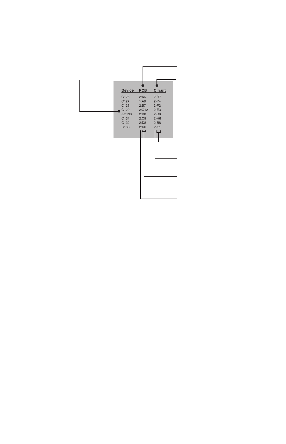
M830P-00 Introduction E1.3
Copyright TEL 01/07/00
Grid Reference Index
This section contains a component grid reference index to help you find components and labelled
pads on the PCB layouts and circuit diagrams. This index lists the components and pads in alpha-
numeric order, along with the appropriate alphanumeric grid references, as shown below:
circuit diagram
reference
PCB layout
reference
components listed
in alphanumeric order
layer number -
1 = top side layer
2 = bottom side layer
component location
on the layer
sheet number
component location
on the sheet

E1.4 Introduction M830P-00
01/07/00 Copyright TEL

M830P-00 T830 VCO PCB Information E2.1
Copyright TEL 01/07/00
2 T830 VCO PCB
This section contains the following information.
IPN Section Page
220-01176-03 Parts List
Mechanical & Miscellaneous Parts
Grid Reference Index
PCB Layout - Bottom Side
PCB Layout - Top Side
Circuit Diagram
2.3
2.5
2.6
2.7
2.8
2.9

E2.2 T830 VCO PCB Information M830P-00
01/07/00 Copyright TEL

IPN 220-01176-03
M830P-00 T830 VCO PCB Information E2.3
Copyright TEL 01/07/00
T830 VCO Parts List (IPN 220-01176-03)
How To Use This Parts List
The components listed in this parts list are divided into two main types: those with a circuit reference (e.g. C2, D1, R121, etc.) and
those without (miscellaneous and mechanical).
Those with a circuit reference are grouped in alphabetical order and then in numerical order within each group. Each component
entry comprises three or four columns: the circuit reference, variant (if applicable), IPN and description. A letter in the variant column
indicates that this is a variant component which is fitted only to the product type listed. Static sensitive devices are indicated by an (S)
at the start of the description column.
The mechanical and miscellaneous section lists the variant and common parts in IPN order.
The Parts List Amendments box below lists component changes that took place after the parts list and diagrams in this section were
compiled. These changes (e.g. value changes, added/deleted components, etc.) are listed by circuit reference in alphanumeric order
and supersede the information given in the parts list or diagrams. Components without circuit references are listed in IPN order.
Parts List Amendments
#C6 Tx High (A): incorrectly listed as 22p (015-22220-01) - correct value is 18p (015-22180-01).
Tx High (A): changed from 18p (015-22180-01) to 15p (015-22150-01) to improve the loop voltage tuning range
at the top of the band (710943/44).

IPN 220-01176-03
E2.4 T830 VCO PCB Information M830P-00
01/07/00 Copyright TEL
Ref Var IPN Description Ref Var IPN Description
C2 015-23680-08 CAP CER 0805 680P 10% X7R 50V
#C3 A 015-22180-01 CAP CER 0805 18P 5% NPO 50V
#C3 B 015-22180-01 CAP CER 0805 18P 5% NPO 50V
#C4 A 015-22220-01 CAP CER 0805 22P 5% NPO 50V
#C4 B 015-22220-01 CAP CER 0805 22P 5% NPO 50V
#C5 A 015-22220-01 CAP CER 0805 22P 5% NPO 50V
#C5 B 015-22220-01 CAP CER 0805 22P 5% NPO 50V
#C6 A 015-22220-01 CAP CER 0805 22P 5% NPO 50V
#C6 B 015-22180-01 CAP CER 0805 18P 5% NPO 50V
#C7 A 015-22270-01 CAP CER 0805 27P 5% NPO 50V
#C7 B 015-22330-01 CAP CER 0805 33P 5% NPO 50V
C8 015-23120-01 CAP CER 0805 120P 5% NPO 50V
C9 015-23680-08 CAP CER 0805 680P 10% X7R 50V
C10 015-21220-01 CAP CER 0805 2P2+-1/4P NPO 50V
C11 015-23680-08 CAP CER 0805 680P 10% X7R 50V
C12 015-23680-08 CAP CER 0805 680P 10% X7R 50V
C13 025-08100-02 CAP TANT BEAD 10M 10% 16V
C14 015-23680-08 CAP CER 0805 680P 10% X7R 50V
C15 015-23680-08 CAP CER 0805 680P 10% X7R 50V
C16 015-22560-01 CAP CER 0805 56P 5% NPO 50V
C17 015-22560-01 CAP CER 0805 56P 5% NPO 50V
C18 015-23680-08 CAP CER 0805 680P 10% X7R 50V
C19 015-05470-08 CAP CER 1206 47N 10% X7R 50V
C20 015-23680-08 CAP CER 0805 680P 10% X7R 50V
C21 015-23680-08 CAP CER 0805 680P 10% X7R 50V
C22 015-23680-08 CAP CER 0805 680P 10% X7R 50V
C23 015-21820-01 CAP CER 0805 8P2+-1/4P NPO 50V
C24 015-21680-01 CAP CER 0805 6P8+-1/4P NPO 50V
C25 015-23680-08 CAP CER 0805 680P 10% X7R 50V
#C26 A 036-10000-00 RES M/F 0805 ZERO OHM
#C26 B 036-10000-00 RES M/F 0805 ZERO OHM
CV1 028-02111-00 16PF TRM CAP PISTON PREC.
D1 001-00012-63 S) DIODE VARICAP BB809
D2 001-00012-63 S) DIODE VARICAP BB809
D3 001-00012-63 S) DIODE VARICAP BB809
D4 001-00012-63 S) DIODE VARICAP BB809
L1 056-00021-56 IND FXD 3.3UH AX 10X4.2 PHEN
L2 056-00021-60 IND FXD 330NH AX N/MAG 6.6*2.7
#L3 A 055-01004-00 COIL TROID 103NH 22P 9T T830TX
#L3 B 055-01000-00 COIL TOROID 110NH 22P 10T T830
L4 056-00021-52 IND FXD 820NH 10% NON MAGNETIC
L5 056-00021-56 IND FXD 3.3UH AX 10X4.2 PHEN
L6 052-08135-35 COIL A/W 3.5T/3.5MM HOR 0.8MM
L7 056-00021-56 IND FXD 3.3UH AX 10X4.2 PHEN
L8 052-08130-45 COIL A/W 4.5T/3.0MM HOR 0.8MM
Q1 000-10003-10 S) XSTR SMD BFJ310 JFET UHF
Q2 000-10057-10 S) XSTR SMD BR571 NPN SOT23
Q3 000-10057-10 S) XSTR SMD BR571 NPN SOT23
Q4 000-10008-57 S) XSTR SMD BCW70 PNP SOT23 SS
Q5 000-00032-47 S) XSTR MRF559 NPN XPACK 0.5W
R1 036-12220-00 RES M/F 0805 22E 5%
R3 036-11470-00 RES M/F 0805 4E7 10%
#R5 A 036-13390-00 RES M/F 0805 390E 5%
#R5 B 036-13390-00 RES M/F 0805 390E 5%
R6 036-12560-00 RES M/F 0805 56E 5%
R7 036-14100-00 RES M/F 0805 1K 5%
R8 036-12560-00 RES M/F 0805 56E 5%
R9 036-14100-00 RES M/F 0805 1K 5%
R10 036-12100-00 RES M/F 0805 10E 5%
R11 036-14270-00 RES M/F 0805 2K7 5%
R12 036-13180-00 RES M/F 0805 180E 5%
R13 036-12220-00 RES M/F 0805 22E 5%
R14 036-12560-00 RES M/F 0805 56E 5%
R15 036-12220-00 RES M/F 0805 22E 5%
R16 036-13270-00 RES M/F 0805 270E 5%
R17 036-13270-00 RES M/F 0805 270E 5%
R18 036-12180-00 RES M/F 0805 18E 5%
R19 036-14100-00 RES M/F 0805 1K 5%
R20 036-14680-00 RES M/F 0805 6K8 5%
R21 036-14100-00 RES M/F 0805 1K 5%
R22 036-14220-00 RES M/F 0805 2K2 5%
R23 036-12180-00 RES M/F 0805 18E 5%
R24 036-12220-00 RES M/F 0805 22E 5%
R25 036-13220-00 RES M/F 0805 220E 5%
Variant
Code Description T837
(MHz)
A Tx high 148 - 174
B Tx low 136 - 156

IPN 220-01176-03
M830P-00 T830 VCO PCB Information E2.5
Copyright TEL 01/07/00
IPN Description IPN Legend Description
T830 VCO Mechanical & Miscellaneous Parts (220-01176-03)
220-01176-03 PCB T83X VCO
240-00025-36 PLUG 32WAY 1ROW PC MTG HARWIN
345-00040-10 SCRW M3X6MM P/POZ ST BZ
345-00060-08 SCRW M5 X 16 CH SLOT PLASTIC
350-00016-42 SPACER 5MM HI 8MM ST 2.5MM HO
352-00010-14 NUT M5 HEX PLASTIC T800 TOROID
353-00010-10 WSHR M3 FLAT 7MMX0.6MM ST BZ
353-00010-13 WSHR M3 S/PROOF INT BZ
353-00010-41 WSHR M6 NYLON BULTE LOCK

IPN 220-01176-03
E2.6 T830 VCO PCB Information M830P-00
01/07/00 Copyright TEL
Device PCB Circuit Device PCB CircuitDevice PCB Circuit Device PCB Circuit
T830 VCO Grid Reference Index (IPN 220-01176-03)
How To Use This Grid Reference Index
The first digit in the PCB layout reference is a "1" or "2", indicating the top or bottom side layout respectively, and the last two charac-
ters give the location of the component on that diagram.
The first digit in the circuit diagram reference is the sheet number, and the last two characters give the location of the component on
that sheet.
C2 1:B7 1-B3
#C3 1:C6 1-D4
#C4 1:C6 1-D4
#C5 1:D6 1-D3
#C6 1:C5 1-E4
#C7 1:D5 1-E3
C8 1:D6 1-F3
C9 1:D4 1-H3
C10 1:C4 1-F3
C11 1:C4 1-G4
C12 1:D8 1-F6
C13 1:D7 1-G6
C14 1:C3 1-G5
C15 1:C4 1-H5
C16 1:B3 1-J5
C17 1:B3 1-J4
C18 1:B2 1-J5
C19 1:D1 1-J6
C20 1:D3 1-J7
C21 1:E3 1-K6
C22 1:C3 1-K5
C23 1:C2 1-K4
C24 1:C2 1-L4
C25 1:C2 1-L5
#C26 1:C5 1-D4
C40 1:D5 1-D3
CV1 1:C5 1-D3
D1 1:C7 1-B4
D2 1:C7 1-C4
D3 1:D7 1-B3
D4 1:D7 1-C3
L1 1:C8 1-B3
L2 1:B7 1-C3
#L3 1:B6 1-D4
L4 1:D6 1-E3
L5 1:D7 1-F6
L6 1:A4 1-J4
L7 1:D2 1-K6
L8 1:C2 1-L5
PL-2 2:B4 2-F3
PL-3 2:C3 2-G3
PL-4 2:C8 2-F4
PL-5 2:C1 2-G4
Q1 1:C6 1-F3
Q2 1:D4 1-G3
Q3 1:C4 1-G4
Q4 1:D2 1-K7
Q5 1:B3 1-K5
R1 1:B8 1-B3
R3 1:C7 1-C4
#R5 1:D6 1-F3
R6 1:D4 1-G3
R7 1:D3 1-G3
R8 1:D4 1-G3
R9 1:D3 1-G4
R10 1:C4 1-G4
R11 1:C3 1-G5
R12 1:C4 1-G5
R13 1:B3 1-G6
R14 1:C7 1-F5
R15 1:D8 1-G6
R16 1:B4 1-H4
R17 1:A4 1-H4
R18 1:B4 1-H5
R19 1:B4 1-H6
R20 1:E2 1-J6
R21 1:B2 1-K6
R22 1:D2 1-J7
R23 1:D2 1-K7
R24 1:B2 1-K5
R25 1:C3 1-K5
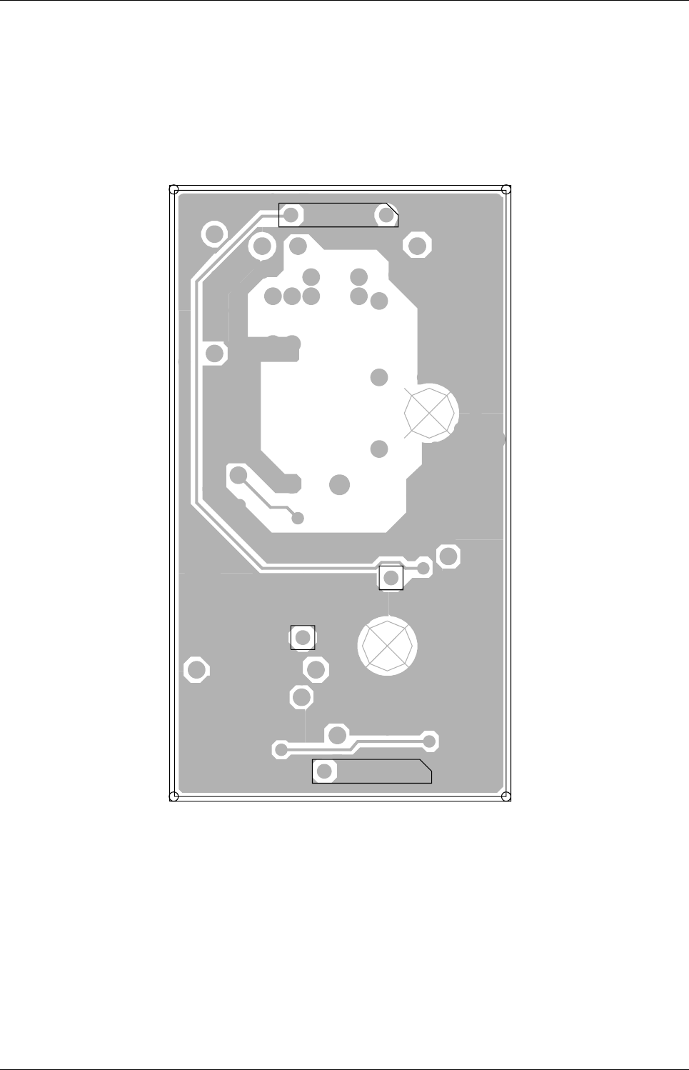
IPN 220-01176-03
M830P-00 T830 VCO PCB Information E2.7
Copyright TEL 01/07/00
T830 VCO PCB - Bottom Side
220-01176-03
PL-5
PL-4
PL-2
PL-3
2
1
3
4
5
6
7
8
ABCDE
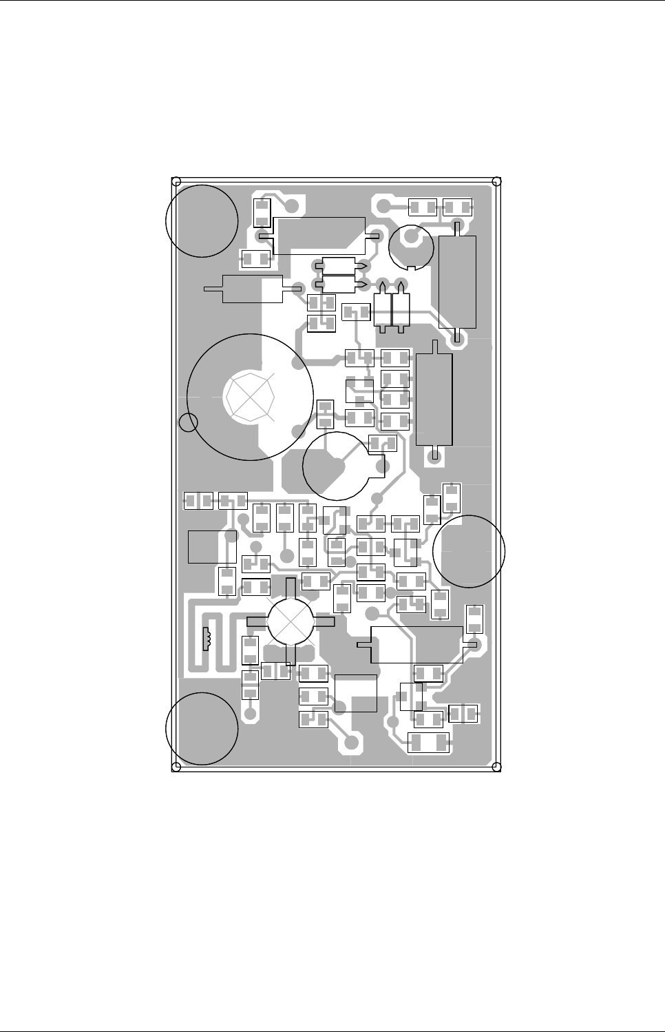
IPN 220-01176-03
E2.8 T830 VCO PCB Information M830P-00
01/07/00 Copyright TEL
T830 VCO PCB - Top Side
220-01176-03
*C26
*C3
*C4 *C5
*C6 *C7
*L3
*R5
C10
C11
C12
C13
C14
C15
C16
C17
C18
C19
C2
C20
C21
C22
C23
C24
C25
C40
C8
C9
CV1
D1
D2
D3D4
L1
L2
L4
L5
L6
L7
L8
PCB
Q1
Q2
Q3
Q4
Q5
R1
R10
R11
R12
R13
R14
R15
R16
R17 R18
R19
R20
R21
R22
R23
R24
R25
R3
R6
R7
R8
R9
SCREW1
SCREW2
SCREW3
TBADMARK
*C26
*C3
*C4 *C5
*C6 *C7
*L3
*R5
C10
C11
C12
C13
C14
C15
C16
C17
C18
C19
C2
C20
C21
C22
C23
C24
C25
C40
C8
C9
CV1
D1
D2
D3D4
L1
L2
L4
L5
L6
L7
L8
PCB
Q1
Q2
Q3
Q4
Q5
R1
R10
R11
R12
R13
R14
R15
R16
R17 R18
R19
R20
R21
R22
R23
R24
R25
R3
R6
R7
R8
R9
SCREW1
SCREW2
SCREW3
TBADMARK
3
2
1
4
5
6
7
8
ABCDE

M830P-00 FI
Copyright TEL 01/07/00
Part F Installation
This part of the manual is divided into the sections listed below. These sections give a
brief description of the basic rack mounting and wiring procedures for the T837 exciter
and T839 power amplifier.
Section Title Page
1
1.1
1.2
1.3
1.4
T837 Installation
Rack Mounting
Rack Wiring
Power Supply
Reverse Polarity & Overvoltage Protection
1.1
1.1
1.1
1.1
1.1
2
2.1
2.2
2.3
2.4
T838/839 Installation
Rack Mounting
Rack Wiring
Power Supply
Reverse Polarity & Overvoltage Protection
2.1
2.1
2.1
2.2
2.2
3 N-Type Connector Assembly 3.1
Figure Title Page
1.1
1.2
1.3
T800-41-0002 Double Guide Kit
T837 Chassis Connectors
T837 D-Range 1 Wiring - Rear View
1.1
1.1
1.1
2.1
2.2
2.3
2.4
T800-45-0001 PA Guide Kit
T838/839 Chassis Connectors
T838/839 PA In Latched Position
T838/839 D-Range Wiring - Rear View
2.1
2.1
2.1
2.1
3.1 N-Type Plug Assembly Details 3.1

FII M830P-00
01/07/00 Copyright TEL
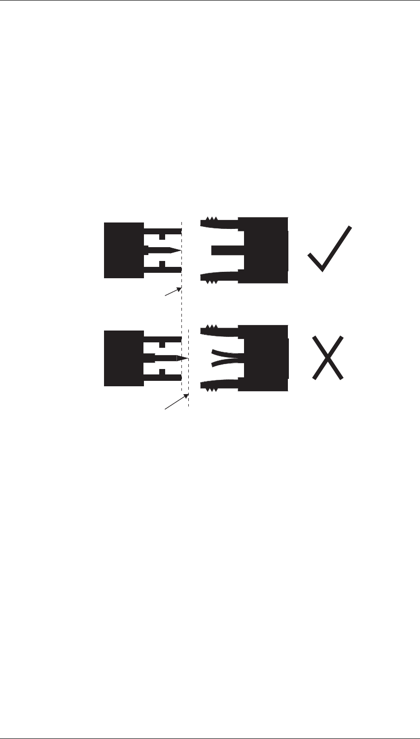
M830P-00 N-Type Connector Assembly F3.1
Copyright TEL 01/07/00
3 N-Type Connector Assembly
Make sure that any N-type plugs connected to Tait equipment are assembled according
to the manufacturer’s instructions. It is particularly important that the centre pin in the
plug is positioned correctly:
• if the pin is positioned too far back in the plug, it may not make good contact
with the socket;
• if the pin protrudes too far (as shown in Figure 3.1), or is not straight, it may
damage the socket when the plug is screwed in.
Figure 3.1 N-Type Plug Assembly Details
Hand ti
g
hten only
N-Type Plug and Socket Cross-section
Correct pin position No damage to socket
Will damage socket
Extended pin position

F3.2 N-Type Connector Assembly M830P-00
01/07/00 Copyright TEL

M830P-00 GI
Copyright TEL 01/07/00
Part G T800-28-0X00 Paging Rack Frame
This part of the manual is divided into the sections listed below. These sections provide
some brief information on the T800-28-0X00 paging rack frame and its associated back-
plane PCB, the T800-55-0000.
Section Title Page
1 T800-28-0X00 General Information 1.1
2 T800-55-0000 Backplane PCB 2.1
Figure Title Page
2.1
2.2
2.3
2.4
T800-55-0000 PL1 Wiring
T800-55-0000 PCB Layout - Top Side (Outer)
T800-55-0000 PCB Layout - Bottom Side (Inner)
T800-55-0000 Circuit Diagram
2.2
2.3
2.4
2.5

GII M830P-00
01/07/00 Copyright TEL

M830P-00 T800-28-0X00 General Information G1.1
Copyright TEL 01/07/00
1 T800-28-0X00 General Information
The T800-28-0X00 is a single channel rack frame with a maximum output of 100W and
provision for a high stability oscillator to enable the paging function, as described
below:
Operational Characteristics • single channel - paging
• up to 100W RF output
• speaker/programming panel
• high stability oscillator
•DC line fuse
•earth stud
• backplane PCB interface
Power Supply Options • T800-28-0000 AC only
• T800-28-0100 external DC only
• T800-28-0200 AC and external DC
• T800-28-0300 AC and battery
• T800-28-0400 external DC and battery
• T800-28-0500 AC and external DC and battery
Configuration Options • duplexer
•coaxial relay
• fans - single or double
• interfaces to TA703-00-XXXX changeover module
using TA703-11-0010 installation kit
•microphone
•DC converter
Mechanical Specifications • 5U x 483mm (19") to house up to seven modules
• height 222mm
• width 482mm
• depth 322mm plus 50mm clearance space
• weight 25W - 12.75kg
50W - 16.5kg
100W - 16.85kg

G1.2 T800-28-0X00 General Information M830P-00
01/07/00 Copyright TEL

M830P-00 T800-55-0000 Backplane PCB G2.1
Copyright TEL 01/07/00
2 T800-55-0000 Backplane PCB
The T800-55-0000 paging backplane PCB is designed for use in the T800-28-0X00 paging
rack frame. The PCB mounts across the rear panel of the T800-41-0003 triple module
rack frame guide, and has provision for the following modules:
• high stability oscillator
• repeater/link receiver (optional)
• paging exciter/transmitter (25, 50 or 100W).
These modules plug directly into the D-range sockets provided on the inner side of the
PCB (both D-range 1 and D-range 2 are provided for). The other side of the PCB fea-
tures:
• a programming port
• two DIP switches for external channel selection
• one 25-way OEM D-range connector (refer to Figure 2.1)
• one 11-way D-range connector with provision for an external frequency refer-
ence.
The T800-55-0000 also allows the fitting of an optional link transmitter/repeater, but
will not accept personality PCBs.

G2.2 T800-55-0000 Backplane PCB M830P-00
01/07/00 Copyright TEL
Figure 2.1 T800-55-0000 PL1 Wiring
Pin Function
1Rx line 1
2 Rx aux 2
3 Rx aux 1
4Rx line 4
5Tx line 1
6POCSAG data
7 lock detect
8Tx line 4
9 signal strength (RSSI)
10 speaker +ve
11 Tx tone input
12 reverse power alarm
13 0V
14 Rx gate
15 Tx key
16 Rx relay common
17 Rx relay normally open
18 Rx inhibit
19 Data/speech (mode select)
20 opto key +
21 opto key -
22 forward power alarm
23
24 Rx audio 1
25 13.8V (fused)
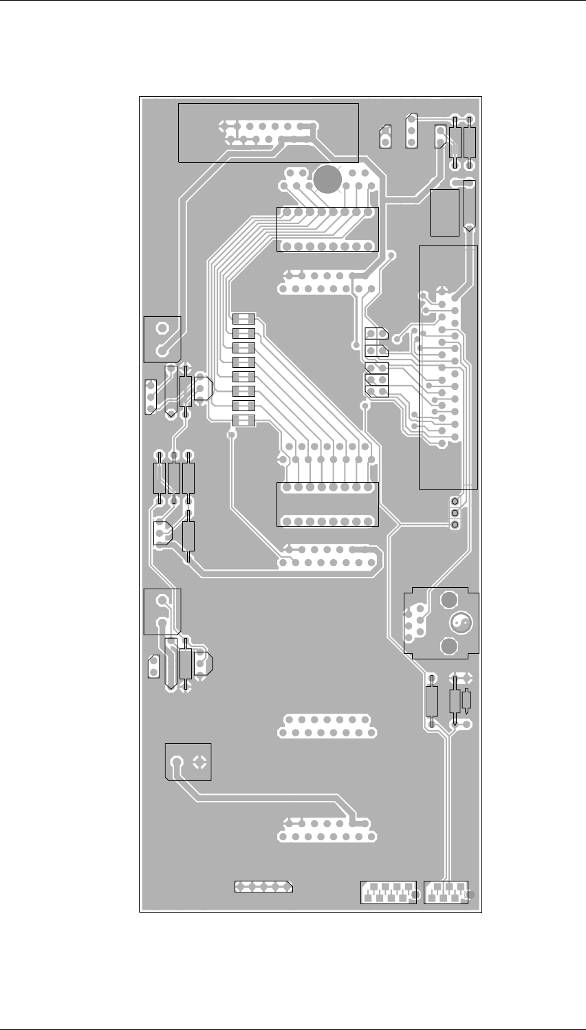
M830P-00 T800-55-0000 Backplane PCB G2.3
Copyright TEL 01/07/00
Figure 2.2 T800-55-0000 PCB Layout - Top Side (Outer)
2
ED
3
C FB GA
1
PL1
1
R1
F1
14
-
25
13
R2
SK2
CN1
S2
S2
RJ1
D5
R3
3
+
LN1
2
D2
TP1
D1
TP2
CHANNEL CHANGE LINKS
FAN CONTROL
1
LN5 2
SK6
15
8
SK7
1
Q1
S1
S1
R4
220-01582-02
111111
10 15 15 15 15 15 88888
6
LN2
-
CCL8
SK4
R8
F1
HOLDER
LINK
T800-55-0000
R7
HI/LO
++
R6
SK8
R5
SK9
D4
D3
Q2
CN2
SK3
Q3
LN4
R9
SK1
CN3
SK5
-
CCL1
LN9
LOCK DETECT 2
RELAY
SIG STRENGTH
LN10
FAN
TP3
LN6
LINE 4
CENTRE
LN7DATA CONNECT
LINE 1
13V8
LN8
LOCK DETECT 1
RX GATE TO TX KEY
RX INHIBIT
LN3 -35
MODE SELECT
1
3
LN5 FAN CONTROL
1-2
2-3 TX KEY
FAN PERM ON
CCL1
CCL2
CCL3
CCL4
CCL5
CCL6
CCL7
CCL8
CN1CN2
CN3
D1
D2
D3 D4
D5
F1
LN1
LN10
LN11
LN2
LN3
LN4
LN5
LN6
LN7
LN8
LN9
PL1
Q1
Q2Q3
R1
R2
R3
R4 R5
R6
R7 R8R9
RJ1
S1 S2
SK7
SK8
SK9
TP1 TP2 TP3
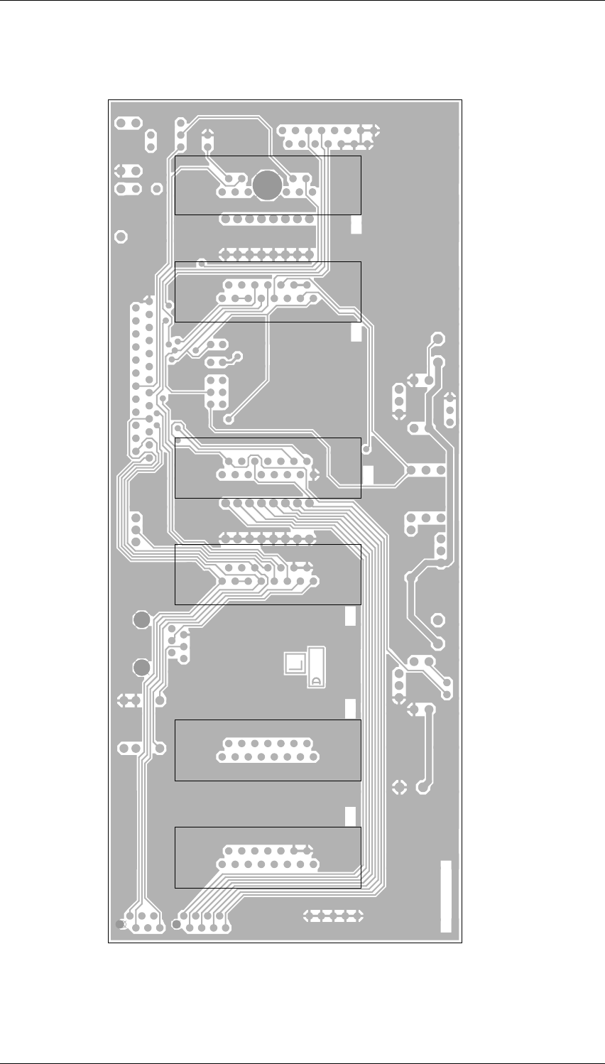
G2.4 T800-55-0000 Backplane PCB M830P-00
01/07/00 Copyright TEL
Figure 2.3 T800-55-0000 PCB Layout - Bottom Side (Inner)
SK2
220-01582-02
SK4 SK5
SK3SK1 SK6
3
2
D
1
BCEFG A
SK1 SK2 SK3 SK4 SK5 SK6

M830P-00 HI
Copyright TEL 01/07/00
Part H T800 Ancillary Equipment
This Part of the manual features a brief description of the major ancillaries that may be
used with T800 Series II equipment. For a comprehensive list of available ancillary
equipment, please contact your nearest Tait Dealer or Customer Service Organisation.
Section Page
Programming Kits 1
General Ancillaries 2
External Frequency Reference 2
Rack Frame Guides 3
Rack Frame Ancillaries 5
Front Panels 6
Power Supplies 7

HII M830P-00
01/07/00 Copyright TEL

M830P-00 T800 Ancillary Equipment H1
Copyright TEL 01/07/00
T800 Ancillary Equipment
Programming Kits
T800-01-0000
The T800-01-0000 kit is used for programming T800 Series II base station equipment
using a standard IBM (or compatible) PC.
The kit comprises the following items:
PGM800Win programming software user's manual
PGM800Win Windows based programming software on 3ë" floppy discs
T800-01-0002 programming cable.
T800-01-0001
The T800-01-0001 kit is the same as the T800-01-0000 kit described above, but with the
addition of the T800-01-0004 module programming interface.
T800-01-0002
The T800-01-0002 programming cable connects the PC directly to the programming
socket on the T800 Series II rack frame speaker panel or backplane PCB, thus enabling
T800 Series II modules to be read or programmed while in the rack frame. It can also
connect to the programming socket on the T800-01-0004 programming module interface
if the module is to be read or programmed while out of the rack frame.
T800-01-0003
The T800-01-0003 programming kit contains a T800-01-0002 programming cable and a
T800-01-0004 programming module interface.
T800-01-0004
The T800-01-0004 programming module interface is designed to allow a PC to connect
directly to a T800 Series II module. It comprises a small PCB on which is mounted a
D-range socket, a programming socket, a Micromatch socket and a DC input connector.
The T800-01-0004 plugs directly into D-range 1 or D-range 2 (selected by a switch on the
PCB), or into SK805 in the microcontroller compartment via the supplied ribbon cable
loom, and is then connected to the PC with a T800-01-0002 programming cable.
Refer to the T800 Ancillary Equipment Service Manual for more information.

H2 T800 Ancillary Equipment M830P-00
01/07/00 Copyright TEL
General Ancillaries
T004-72 RF Coaxial Relay
The T004-72 is an RF coaxial relay assembly fitted with three female N-type connectors,
and comes complete with a mounting bracket and two coaxial cables terminated in male
N-type connectors. It can be used, for example, in base station applications where the
receiver and transmitter share the same antenna, in which case it can be driven by the
T800 Series II transmitter/exciter relay driver.
External Frequency Reference
T801-10 OCXO Module
The T801-10 OCXO module provides a high stability frequency source to which the syn-
thesiser within a T800 Series II base station can be locked. This will provide T800 Series
II transmitters with the frequency stability required for simulcast transmission. The
master standard within the T801-10 is a high quality ovenised crystal oscillator (OCXO).
Three outputs are provided on the rear panel, which allows up to three T800 Series II
transmitters to be referenced to the source oscillator.
Refer to M801-10.

M830P-00 T800 Ancillary Equipment H3
Copyright TEL 01/07/00
Rack Frame Guides
T800-41-0001
The T800-41-0001 rack frame guide is designed to fit into a T800 Series II rack frame and
will accept one T800 Series II module (except for power supplies and power amplifiers
which must use their own guides). It is supplied disassembled and comprises a top and
bottom rail, a rear panel, two D-range sockets and mounting screws.
T800-41-0002
The T800-41-0002 rack frame guide is designed to fit into a T800 Series II rack frame and
will accept two T800 Series II modules (except for power supplies and power amplifiers
which must use their own guides). It is supplied disassembled and comprises two top
and bottom rails, a double width rear panel, four D-range sockets and mounting screws.
T800-41-0003
The T800-41-0003 rack frame guide is designed to fit into a T800 Series II rack frame and
will accept three T800 Series II modules (except for power supplies and power amplifi-
ers which must use their own guides). It is supplied disassembled and comprises three
top and bottom rails, a triple width rear panel, six D-range sockets and mounting
screws.
T800-41-0004
The T800-41-0004 rack frame guide is designed to fit into a T800 Series II rack frame and
will accept four T800 Series II modules (except for power supplies and power amplifiers
which must use their own guides). It is supplied disassembled and comprises four top
and bottom rails, a four-module wide rear panel, eight D-range sockets and mounting
screws.
T800-42-0000
The T800-42-0000 rack frame guide will allow a duplexer to be mounted in a T800 Series
II rack frame. It occupies a single module space and comprises a folded metal chassis,
mounting brackets and screws.

H4 T800 Ancillary Equipment M830P-00
01/07/00 Copyright TEL
T800-42-0001
The T800-42-0001 rack frame guide is the same as the T800-42-0000 described above, but
with the addition of a duplexer front panel.
T800-42-0002
The T800-42-0002 rack frame guide is the same as the T800-42-0000 described above, but
with the addition of a blank front panel.
T800-43-0000
The T800-43-0000 rack frame guide is designed to fit into a T800 Series II rack frame and
will accept one T300 or T1500 Series module (e.g. T318-02, T1511). It is supplied disas-
sembled and comprises a top and bottom rail, two T300 D-range socket boxes and
mounting screws. The T800-43-0000 is not compatible with the T800 Series II rack frame
backplane PCB. Consult your nearest Tait Dealer or Customer Service Organisation for
more details about T300/T1500 Series compatibility with T800 Series II rack frames.
T800-43-0001
The T800-43-0001 is the same as the T800-43-0000 but is supplied with only one D-range
socket box.
T800-44-0000
The T800-44-0000 rack frame guide is designed to fit into a T800 Series II rack frame and
will accept one T800 Series II power supply. It comprises a top and bottom rail and
mounting screws.
T800-45-0000
The T800-45-0000 rack frame guide is designed to fit into a T800 Series II rack frame and
will accept one T800 Series II 50W power amplifier. It comprises a top guide stop, a bot-
tom guide rail and mounting screws.
T800-45-0001
The T800-45-0001 rack frame guide is designed to fit into a T800 Series II rack frame and
will accept one T800 Series II 100W power amplifier. It comprises a top guide stop, a
bottom guide rail, extra mounting brackets for the double width front panel and mount-
ing screws.

M830P-00 T800 Ancillary Equipment H5
Copyright TEL 01/07/00
Rack Frame Ancillaries
T800-13-0000 Extender Rail
The T800-13-0000 extender rail allows a T800 Series II receiver, exciter or transmitter to
be operated out of the rack frame with the covers off for tuning purposes. It is fitted
with two 15-way D-range connectors.
T800-14-0000 Extender Rail
The T800-14-0000 extender rail is the same as the T800-13-0000, but is intended for
equipment using an external reference (e.g. Quasi-Sync). It thus has one 15-way
D-range, and one 11-way D-range incorporating a miniature RF connector.
T800-19-0000 Rack Mounting Fan
The T800-19-0000 fan is designed to fit into the base of any standard 483mm rack frame
without affecting its ability to house seven modules. The two mounting rails are
secured to the rack frame side panels, and the fan is screwed onto the rails under the
required module. The kit contains all mounting hardware.
T800-19-0010 Rack Mounting Fan
The T800-19-0010 fan is designed to fit into the base of any standard 483mm rack frame
without affecting its ability to house seven modules. The fan is mounted directly onto
the underside of the bottom guide rails with two mounting brackets. The kit contains
all mounting hardware.

H6 T800 Ancillary Equipment M830P-00
01/07/00 Copyright TEL
Front Panels
T800-15-0000 Speaker Panel
A 60mm speaker panel fitted with a 4Ω speaker and programming socket. It comes
complete with mounting hardware and a cable to connect the programming socket to
the backplane PCB.
T800-15-0001 Speaker Panel
A 60mm speaker panel fitted with a 4Ω speaker, complete with mounting hardware.
T800-17-0010 Circuit Breaker Panel
A 60mm front panel fitted with a 10A magnetic circuit breaker. The circuit breaker also
functions as an on/off switch to control the supply of power to the rack frame. The
T800-17-0010 is intended primarily for use with rack frames powered by batteries (or
with a battery back-up supply) and comes complete with mounting hardware.
T800-17-0020 Circuit Breaker Panel
The same as the T800-17-0010, but fitted with a 20A circuit breaker.
T800-40-0000 Blank Panel Fitting Kit
The mounting brackets and screws necessary to fit a T800 Series II 60mm blank front
panel into a T800 Series II rack frame.
T800-40-0001 Blank Panel
A T800 Series II 60mm blank panel complete with mounting brackets and screws.

M830P-00 T800 Ancillary Equipment H7
Copyright TEL 01/07/00
Power Supplies
T808-10-0000 Mains Power Supply
The T808-10-0000 is a switching power supply capable of supplying up to 25A at 11-14V
DC. It requires a mains supply of 230V/50Hz or 115V/60Hz (nominal values) which
can be internally selected with a switch. The T808-10-0000 is designed to power T800
Series II 100W transmitters (plus receivers, etc.) and requires a T800-44-0000 guide to fit
into a T800 Series II rack frame.
Refer to the T800 Ancillary Equipment Service Manual for more information.

H8 T800 Ancillary Equipment M830P-00
01/07/00 Copyright TEL