Tait TEL0042 Base station transmitter User Manual
Tait Limited Base station transmitter
UserManual.wiki
>
Tait
>
TEL0042 User Manual
User manual
Navigation menu
Upload a User Manual
Namespaces
Wiki Guide
HTML
PDF
Info
Views
User Manual
Discussion / Help
Navigation


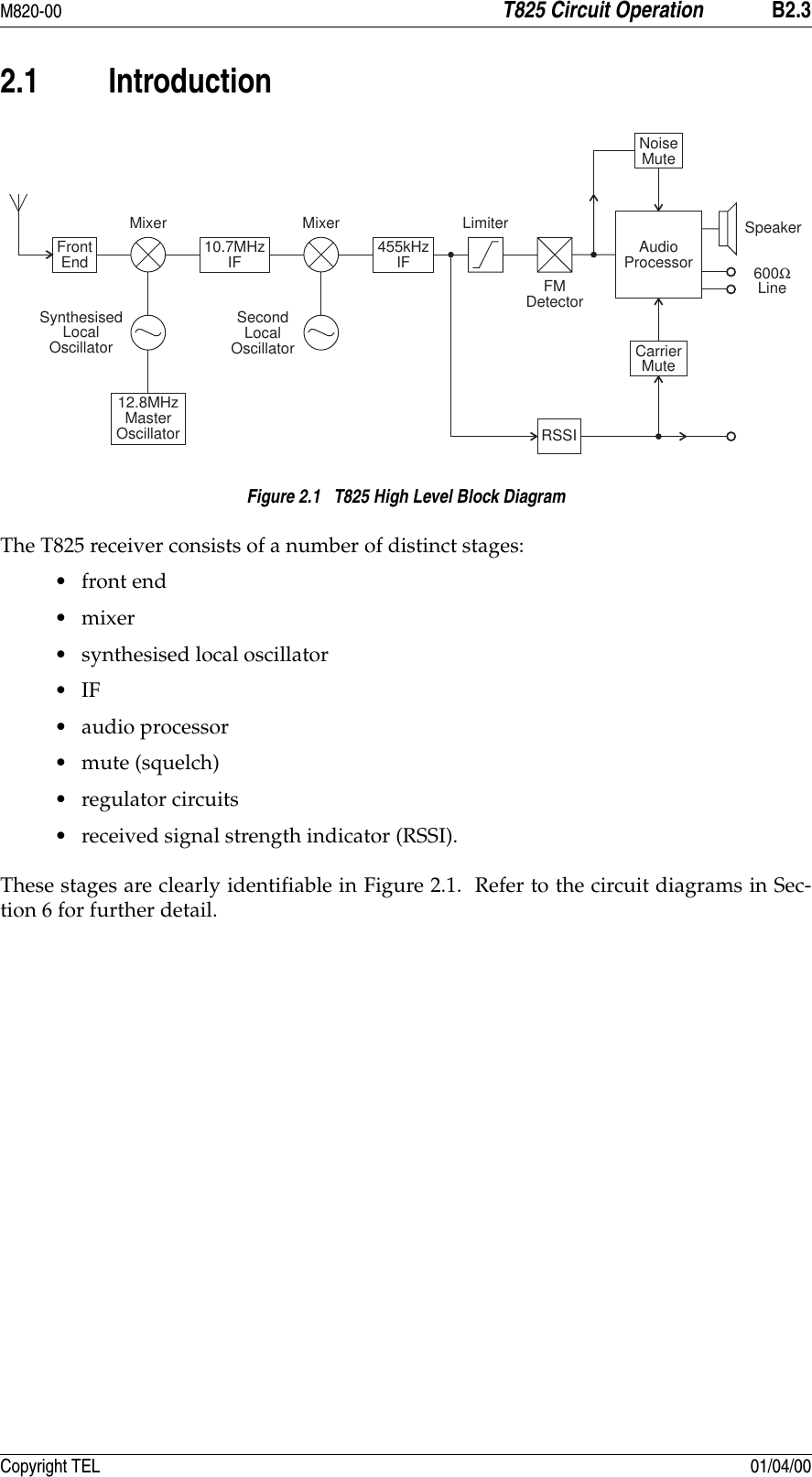
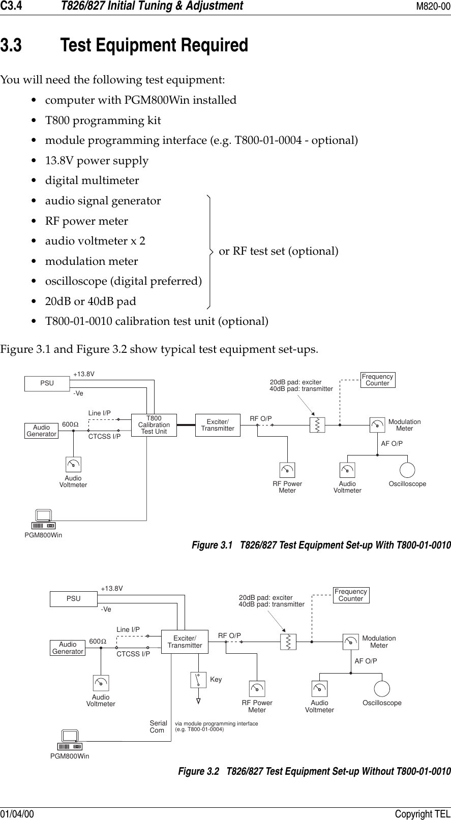
![M820-00 T825 Initial Tuning & Adjustment B3.5Copyright TEL 01/04/003.4 Short Tuning ProcedureUse this procedure only if you want to reprogram the receiver to a frequency outside the2MHz switching range and do not intend to carry out any other major adjustments orrepairs.3.4.1 IntroductionReprogram the operating frequency as described in the PGM800Win program-ming kit (refer to Section 3.2).Remove the top cover (nearest the handle).Set up the test equipment as described in Section 3.3.Set the links in the audio processor section as required (refer to Section 3.5).3.4.2 Synthesiser Alignment• Connect a high impedance voltmeter to PL4-1 or the junction of L1 & R1 in theVCO (this measures the synthesiser loop voltage).•Single Channel Tune VCO trimmer &VC1-RX for a synthesiser loop volt-age of 9V.Multichannel Tune VCO trimmer &VC1-RX for a synthesiser loop volt-age of 9V on the middle channel.If there is no middle channel, tune &VC1-RX so that thechannels are symmetrically placed around a loop voltageof 9V.All channels should lie within the upper and lower limitsof 13V and 5V respectively.Do not attempt to program channels with a greater fre-quency separation than the specified switching range of2MHz.3.4.3 Front End AlignmentNote 1: In this and following sections deviation settings are given first for widebandwidth sets, followed by settings in brackets for narrow bandwidth sets[ ].Note 2: For multichannel operation align the receiver on a frequency in the middleof the required band.Set RV230 (front panel gating sensitivity) fully clockwise.](https://usermanual.wiki/Tait/TEL0042/User-Guide-111477-Page-47.png)
![B3.6 T825 Initial Tuning & Adjustment M820-0001/04/00 Copyright TELInject a strong on-channel RF signal with ±3kHz deviation [±1.5kHz] at 1kHz intothe antenna socket and adjust front end doublets L410, L409, L403 & L402 to givebest sinad.Continually decrease the RF level to maintain 12dB sinad.Readjust L410, L409, L403 & L402 to give best sinad.With PL210 and PL220 connected for de-emphasised audio response, the receiversensitivity should be better than -117dBm, assuming that the audio levels are notbeing overdriven (refer to Section 3.4.5).3.4.4 Mute AdjustmentCarry out the one of the following sets of instructions according to the mute option youhave selected.3.4.4.1 Noise MuteConnect pins 1 & 2 of PL250 to enable the noise mute.Set the RF level to -105dBm with ±3kHz deviation [±1.5kHz] at 1kHz.Set RV230 (front panel gating sensitivity) fully anticlockwise.Adjust RV331 (noise mute gain) fully anticlockwise to close the mute (if necessaryturn off the RF signal and then turn it on again).Rotate RV331 clockwise until the mute just opens.Reset the signal generator for the required opening sinad and adjust RV230 clock-wise until the mute just opens.3.4.4.2 Carrier Level MuteConnect pins 2 & 3 of PL250 to enable the carrier mute and disable the noise mute.Apply an on-channel signal from the RF generator at the required mute openinglevel with ±3kHz deviation [±1.5kHz] at 1kHz.Adjust RV235 (carrier mute) clockwise to close the mute (if necessary, momentar-ily turn off the RF), then slowly adjust it anticlockwise until the mute just opens.The mute should now open at this preset level.3.4.5 Line Amplifier OutputApply an on-channel signal from the RF generator at a level of -70dBm with±3kHz deviation [±1.5kHz] at 1kHz.Adjust RV210 (front panel line level) to set the line level to the required outputlevel.](https://usermanual.wiki/Tait/TEL0042/User-Guide-111477-Page-48.png)
![M820-00 T825 Initial Tuning & Adjustment B3.7Copyright TEL 01/04/003.4.6 CTCSS3.4.6.1 Decoder OperationProgram a CTCSS tone on the default channel using PGM800Win.Set the RF signal generator output to -70dBm.Modulate the generator with both:• a 1kHz tone at ±3kHz deviation [±1.5kHz];• and a CTCSS tone at the programmed frequency at ±500Hz deviation[±300Hz].Check that the receiver gate opens and the front panel "Gate" LED is on.3.4.6.2 Opening SinadEnsure a CTCSS tone is present (as described in Section 3.4.6.1).Adjust RV230 (front panel gating sensitivity) fully clockwise.Reduce the RF signal level to -110dBm.Observe the sinad meter and reduce the RF level until the receiver mute closes.Slowly increase the signal level until the receiver mute just opens and stays open.With PL240 pins 1 & 2 linked (high pass filter bypassed), check that the sinad isless than 6dB.Reset the signal generator for the required opening sinad, adjust RV230 fully anti-clockwise, then clockwise until the mute just opens.3.4.6.3 High Pass FilterEnsure a CTCSS tone is present (as described in Section 3.4.6.1).Set the audio processor links as follows:Reset the RF signal generator output to -70dBm and note the line level (measure-ment A).Plug Link FunctionPL210 1 - 2 de-emphasised responsePL220 2 - 3PL230 2 - 3 audio from internal CTCSS speech filterPL240 4 - 5 audio input via PL230 or I/O pad](https://usermanual.wiki/Tait/TEL0042/User-Guide-111477-Page-49.png)
![B3.8 T825 Initial Tuning & Adjustment M820-0001/04/00 Copyright TELReduce the 1kHz generator to zero output and measure the line level again (meas-urement B).Check that measurement B is at least 30dB below measurement A.3.4.7 RSSI (If Used)Align the receiver as instructed in Section 3.6 and Section 3.7.Apply an on-channel signal from the RF generator at a level of -100dBm with±3kHz deviation [±1.5kHz] at 1kHz.Adjust RV330 (RSSI level) to give 4.5V RSSI output on pin 5 of D-range 1 (PL100)when measured with a high impedance DMM.3.5 Audio Processor Links3.5.1 GeneralUse the following table to set up the audio processor to the configuration you require.You should set the audio processor links before carrying out the receiver alignment.The factory settings are shown in brackets [ ].Plug Link FunctionPL210 [1 - 2]2 - 3de-emphasised responseflat responsePL220 1 - 2[2 - 3]flat responsede-emphasised responsePL230a1 - 2[2 - 3]3 - 4audio input via AUDIO-2 padaudio from internal CTCSS speech filteraudio input via I/O pad P250PL240a1 - 2[2 - 3]or3 - 44 - 5bypass high pass filter300Hz high pass filter in circuitaudio input via PL230 or I/O padPL250 [1 - 2]2 - 3noise mutecarrier mutePL260 1 - 2[2 - 3]RX-DISABLE linknot connected](https://usermanual.wiki/Tait/TEL0042/User-Guide-111477-Page-50.png)
![M820-00 T825 Initial Tuning & Adjustment B3.9Copyright TEL 01/04/003.5.2 Audio Processor Linking Details For CTCSSYou must connect the audio processor links correctly according to the CTCSS optionused, as shown in the table below.The conditions stated in the above table are defined as follows:• standard, no CTCSS - no CTCSS or other sub-audio signalling used- audio bandwidth 300Hz to 3kHz- hum & noise -55dB• received CTCSS tone - tone and speech transmitted down 600 ohm line+ speech to line output - audio bandwidth 10Hz to 3kHz- hum & noise -45dB• high pass filtered speech - 400Hz to 3kHz + internal CTCSS detection - hum & noise -30dB with 250.3Hz tone present• external CTCSS detection - decoding performed through the receiver (butexternally)- speech injected back into receiver via "AUDIO-2"and sent down 600 ohm lineNote 1: AUDIO-2 is available on D-range 1 (PL100) pin 7 via the link resistor R160.Although PL100 pin 7 is already assigned to SERIAL-COM, this can be disa-bled by removing R808.Note 2: External CTCSS units can connect in series with the audio chain viaAUDIO-1 and AUDIO-2.Plug Link FunctionPL270 [1 - 2]2 - 3relay linknot connecteda. Refer to Section 3.5.2 for further details.CTCSS Option PL230 PL240standard, no CTCSS 2 - 3 2 - 3received CTCSS + speechpassed to line output 3 - 4 1 - 2high pass filtered speech,internal CTCSS detection 2 - 3 4 - 5external CTCSS detection 1 - 2 4 - 5](https://usermanual.wiki/Tait/TEL0042/User-Guide-111477-Page-51.png)
![B3.10 T825 Initial Tuning & Adjustment M820-0001/04/00 Copyright TEL3.6 Synthesiser Alignment• Ensure that the receiver has been programmed with the required frequenciesusing PGM800Win software.• Connect a high impedance voltmeter to PL4-1 or the junction of L1 & R1 in theVCO (this measures the synthesiser loop voltage).•Single Channel Tune VCO trimmer &VC1-RX for a synthesiser loop volt-age of 9V.Multichannel Tune VCO trimmer &VC1-RX for a synthesiser loop volt-age of 9V on the middle channel.If there is no middle channel, tune &VC1-RX so that thechannels are symmetrically placed around a loop voltageof 9V.All channels should lie within the upper and lower limitsof 13V and 5V respectively.Do not attempt to program channels with a greater fre-quency separation than the specified switching range of2MHz.• The TCXO (=IC700) output frequency should be trimmed when the IF is tuned -refer to Section 3.7.3.7 Alignment Of Receiver Front End And IFNote 1: In this and following sections deviation settings are given first for widebandwidth sets, followed by settings in brackets for narrow bandwidth sets[ ].Note 2: Before carrying out this alignment procedure, check that the solder linksin the receiver front end are set as described in the following table:Align the synthesiser as instructed in Section 3.6. For multichannel operationalign the receiver on a frequency in the middle of the required band.Frequency Range Linked Not Linked66-76MHz #SL400#SL402#SL403#SL405#SL401#SL40476-88MHz #SL401#SL404#SL400#SL402#SL403#SL405](https://usermanual.wiki/Tait/TEL0042/User-Guide-111477-Page-52.png)
![M820-00 T825 Initial Tuning & Adjustment B3.11Copyright TEL 01/04/00Set RV230 (front panel gating sensitivity) fully clockwise.Inject a strong on-channel RF signal with ±3kHz deviation [±1.5kHz] at 1kHz intothe antenna socket and adjust front end doublets L410, L409, L403 & L402 to givebest sinad.Continually decrease the RF level to maintain 12dB sinad.Tune quad coil L330 for maximum audio level.While maintaining a low level unmodulated RF input to the receiver, loosely cou-ple into the first IF an additional high level signal at 10.7MHz - you will hear abeat note.Trim the synthesiser TCXO (=IC700) for zero beat.Note: If a second oscillator is not available, you can connect a frequency counter toIC710 pin 6 (i.e. after the TCXO buffer) via an oscilloscope probe to measurethe TCXO frequency directly (12.8MHz). At this point the voltage level isapproximately 4V p-p.Readjust L410, L409, L403 & L402 to give best sinad.Change the RF signal level to -70dBm and modulate with ±3kHz deviation[±1.5kHz] at 1kHz.Connect plugs PL210 and PL220 to give a flat audio response (refer to Section 3.5).Adjust quad coil L330 and CV300 for minimum audio distortion.Check that the distortion reading is:wide bandwidth ≤2%narrow bandwidth ≤4%.If required, reconnect plugs PL210 and PL220 to give a de-emphasised audioresponse and check that the distortion reading is ≤2% (both bandwidths).Reduce the RF level until 12dB sinad is reached. The receiver sensitivity shouldbe better than -117dBm (de-emphasised) or -111dBm (flat), assuming that theaudio levels are not being overdriven (refer to Section 3.11).](https://usermanual.wiki/Tait/TEL0042/User-Guide-111477-Page-53.png)
![B3.12 T825 Initial Tuning & Adjustment M820-0001/04/00 Copyright TEL3.8 Gating DelayTwo solder links (SL210 & SL220) are provided on the top of the PCB to allow three gatedelay time options, as shown in the table below.*Factory setting.3.9 Noise Mute AdjustmentConnect pins 1 & 2 of PL250 to enable the noise mute.Align the receiver as instructed in Section 3.6 and Section 3.7.Set the RF level to -105dBm with ±3kHz deviation [±1.5kHz] at 1kHz.Set RV230 (front panel gating sensitivity) fully anticlockwise.Adjust RV331 (noise mute gain) fully anticlockwise to close the mute (if necessaryturn off the RF signal and then turn it on again).Rotate RV331 clockwise until the mute just opens.Reset the signal generator for the required opening sinad and adjust RV230 clock-wise until the mute just opens.3.10 Carrier Level MuteConnect pins 2 & 3 of PL250 to enable the carrier mute and disable the noise mute.Apply an on-channel signal from the RF generator at the required mute openinglevel with ±3kHz deviation [±1.5kHz] at 1kHz.Adjust RV235 (carrier mute) clockwise to close the mute (if necessary, momentar-ily turn off the RF), then slowly adjust it anticlockwise until the mute just opens.The mute should now open at this preset level.SL210 SL220 Closing Delaylinked not linked <50ms*not linked linked <25msnot linked not linked <20ms](https://usermanual.wiki/Tait/TEL0042/User-Guide-111477-Page-54.png)
![M820-00 T825 Initial Tuning & Adjustment B3.13Copyright TEL 01/04/003.11 Audio Processor3.11.1 Line Amplifier OutputApply an on-channel signal from the RF generator at a level of -70dBm with±3kHz deviation [±1.5kHz] at 1kHz.Adjust RV210 (front panel line level) to give an output of +10dBm on the 600 ohmline.Check for any clipping or distortion on the oscilloscope.Set the line level to the required output level.3.11.2 Monitor Amplifier Output (Speaker Output)Adjust RV205 (front panel monitor volume) to give an output of 2V rms into a 4ohm resistive load.Check for any clipping or distortion on the oscilloscope.Switch to a 4 ohm speaker and adjust RV205 to the required level.3.12 CTCSS3.12.1 Decoder OperationProgram a CTCSS tone on the default channel using PGM800Win.Set the RF signal generator output to -70dBm.Modulate the generator with both:• a 1kHz tone at ±3kHz deviation [±1.5kHz];• and a CTCSS tone at the programmed frequency at ±500Hz deviation[±300Hz].Check that the receiver gate opens and the front panel "Gate" LED is on.3.12.2 Opening SinadEnsure a CTCSS tone is present (as described in Section 3.12.1).Adjust RV230 (front panel gating sensitivity) fully clockwise.](https://usermanual.wiki/Tait/TEL0042/User-Guide-111477-Page-55.png)
![B3.14 T825 Initial Tuning & Adjustment M820-0001/04/00 Copyright TELReduce the RF signal level to -110dBm.Observe the sinad meter and reduce the RF level until the receiver mute closes.Slowly increase the signal level until the receiver mute just opens and stays open.With PL240 pins 1 & 2 linked (high pass filter bypassed), check that the sinad isless than 6dB.Reset the signal generator for the required opening sinad, adjust RV230 fully anti-clockwise, then clockwise until the mute just opens.3.12.3 High Pass FilterEnsure a CTCSS tone is present (as described in Section 3.12.1).Set the audio processor links as follows:Reset the RF signal generator output to -70dBm and note the line level (measure-ment A).Reduce the 1kHz generator to zero output and measure the line level again (meas-urement B).Check that measurement B is at least 30dB below measurement A.3.13 RSSIAlign the receiver as instructed in Section 3.6 and Section 3.7.Apply an on-channel signal from the RF generator at a level of -100dBm with±3kHz deviation [±1.5kHz] at 1kHz.Adjust RV320 (RSSI level) to give 4.5V RSSI output on pin 5 of D-range 1 (PL100)when measured with a high impedance DMM.Plug Link FunctionPL210 1 - 2 de-emphasised responsePL230 2 - 3 audio from internal CTCSS speech filterPL240 4 - 5 audio input via PL230 or I/O pad](https://usermanual.wiki/Tait/TEL0042/User-Guide-111477-Page-56.png)


![M820-00 T826/827 General Information C1.7Copyright TEL 01/04/001.2.4.2 Modulation CharacteristicsFrequency Response .. flat or pre-emphasised (optional) (below limiting)Line And Microphone Inputs: Pre-emphasised Response- Bandwidth .. 300Hz to 3kHz (WB).. 300Hz to 2.55kHz (NB)Below Limiting .. within +1, -3dB of a 6dB/octavepre-emphasis characteristic Flat Response .. within +1, -2dB of output at 1kHzAbove Limiting Response .. within +1, -2dB of a flat response(ref. 1kHz)Distortion .. 2% max.Hum And Noise: Wide Bandwidth .. -55dB (300Hz to 3kHz [EIA]) typical Narrow Bandwidth .. -50dB (CEPT) Compressor (optional): Attack Time .. 10ms Decay Time .. 800ms Range .. 50dB1.2.4.3 CTCSSStandard Tones .. all 37 EIA group A, B and C tonesplus 13 commonly used tonesFrequency Error .. 0.08% max.(from EIA tones)Generated Tone Distortion .. 1.2% max.Generated Tone Flatness .. flat across 67 to 250.3Hz to within 1dBModulation Level .. adjustableModulated Distortion .. <5%1.2.5 MicrocontrollerAuxiliary Ports:Open Drain Type .. capable of sinking 2.25mA via 2k2ΩVds max. .. 5V](https://usermanual.wiki/Tait/TEL0042/User-Guide-111477-Page-85.png)
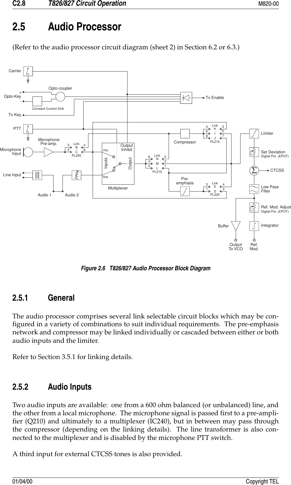
![M820-00 T826/827 Circuit Operation C2.9Copyright TEL 01/04/002.5.3 Keying InputsThere are four ways to key the exciter: • pulling the Tx-Key line low (pin 13 on D-range 1 [PL100]) at the rear of the set);• pushing the "Carrier" button on the front panel - this will inhibit all audio;• using the PTT button on the local microphone, disabling audio from the line;• via the opto-key inputs (pins 11 and 12 on D-range 1 [PL100]) when electricalisolation is required. This features a constant current sink (Q270) to ensure reli-able activation of the opto-coupler (IC250) at low keying voltages.2.5.4 Compressor (Automatic Level Control (ALC))The input signal is fed via a current controlled attenuator (Q230, Q220) to a high gainstage (IC230) from which the output signal is taken. This signal is passed to a compara-tor (IC230) which toggles whenever the audio signal exceeds a DC threshold deter-mined by RV220. Thus, the comparator produces a square wave whose mark-spaceratio is determined by the amplitude of the audio signal. This square wave pumps upthe reservoir capacitor (C233) which controls the attenuator (Q230, Q220), thus complet-ing the feedback loop.The compression level is set by adjustment of the comparator threshold (RV220).Note: Although the high dynamic range of the compressor allows the use of verylow audio signal levels, such conditions will be accompanied by a degrada-tion of the signal-to-noise ratio. Very low audio input levels should there-fore be avoided where possible.2.5.5 Outputs To ModulatorsThe output signal from the limiter (IC210, IC230) is added with a CTCSS tone at a sum-ming amplifier (IC260). The signal is then low pass filtered (IC260) and split to supplythe two modulators.Since the VCO modulator is a true frequency modulator, its audio is simply buffered(IC260). The reference modulator, however, is a phase modulator and its audio mustfirst be integrated (IC210).It is vital that the audio levels to the modulators are accurately set, relative to eachother. Hence the inclusion of level adjustment in the reference modulator path. Onceset, adjustments to absolute deviation may be made only by IC220, a 256-step 10k elec-tronic potentiometer (EPOT), which is controlled via PGM800Win. The EPOT is madeup of 256 resistive sections (representing approximately 39Ω each) which can be indi-vidually addressed by the microcontroller. Each section can be switched in or out of cir-cuit to achieve the required total resistance, thus adjusting the absolute deviation level.](https://usermanual.wiki/Tait/TEL0042/User-Guide-111477-Page-97.png)

![C3.6 T826/827 Initial Tuning & Adjustment M820-0001/04/00 Copyright TEL3.4.4 Two Point Modulation AdjustmentNote 1: In this and following sections deviation settings are given first for widebandwidth sets, followed by settings in brackets for narrow bandwidth sets[ ].Note 2: The reference modulation and limiter adjustments are controlled by 256-step electronic potentiometers (EPOTs), which are adjusted via the “Refer-ence Modulation” and “Deviation” settings in PGM800Win. This allows thetwo point modulation and deviation settings to be adjusted for each chan-nel.Note 3: To optimise the modulation response across the switching range, repeatsteps 1-4 below for each channel that will be used (usually needed only fordata applications). In applications where the modulation response is lesscritical (e.g. voice use only), carry out steps 1-4 below on the middle channeland use the “EPOT Fill” option1 in PGM800Win to copy the value to theother channels.Note 4: If you are using an RF test set, turn the low pass filter off and set the highpass filter to 15kHz before beginning this procedure.1. Inject an audio signal of 450Hz 1.5V rms (+5dBm) into the CTCSS input (D-range1 (PL100) pin 8). Key the transmitter by earthing the Tx-Key line.2. Adjust the output from the audio generator to obtain ±3kHz [±1.5kHz] deviationat 450Hz.3. Change the input frequency to 100Hz and, using PGM800Win, adjust the value ofthe “Reference Modulation” EPOT setting for the current channel to obtain ±3kHz[±1.5kHz] deviation (you can use either the mouse or up and down arrow keys).4. Change the input frequency back to 450Hz.Repeat steps 2 and 3 above until the deviations achieved at the two input frequen-cies are within 0.2dB of each other. You will need to do this at least four times.5. Sweep the audio between 50 and 300Hz for peaks.Note: A peak between 50 and 300Hz will indicate a fault condition, i.e:- incorrect set-up or - modulation circuitry fault. The specification window is ±1dB relative to 150Hz from 65 to 260Hz.1. Use the “EDIT FILL” button on the tool bar or go to “Edit”, “Fill”, “Epot Settings” on the menu bar.](https://usermanual.wiki/Tait/TEL0042/User-Guide-111477-Page-108.png)
![M820-00 T826/827 Initial Tuning & Adjustment C3.7Copyright TEL 01/04/003.4.5 CTCSS Encoder (If Used)Program a CTCSS tone on the default channel using PGM800Win.If you are using an RF test set, turn off the 300Hz high pass filter.Key the T826/827 with the front panel "Carrier" switch.Adjust RV805 (CTCSS level adjust) to give ±500Hz [±250Hz] deviation.Set the maximum deviation as per Section 3.4.6.3.4.6 FM Deviation (Limiter) AdjustmentNote: If the T826/827 will be used over the whole 8MHz switching range, youmust set the deviation for each channel. However, if the module will beused on frequencies that cover only a 1MHz (or less) switching range, youcan set the deviation on the middle channel and use this value for all otherchannels with the “EPOT Fill” option in PGM800Win.Inject 1kHz at -10dBm into the line input (D-range 1 (PL100) pins 1 & 4; pins 2 & 3shorted).Adjust RV210 (line sensitivity) fully clockwise and key the transmitter by earthingthe Tx-Key line. Using PGM800Win, adjust the value of the “Deviation” EPOTsetting for the current channel to obtain a deviation limit of ±4.7kHz [±2.3kHz](you can use either the mouse or up and down arrow keys).Sweep the audio frequency from 100Hz to 4kHz and ensure that the maximumdeviation does not exceed ±4.7kHz [±2.3kHz]. Readjust “Deviation” if necessaryvia PGM800Win.3.4.7 Line-in Level AdjustmentRemove the CTCSS signal (if used).Set the injected signal at the line input to the required line level (typically -10 to-20dBm).Adjust RV210 (line sensitivity) to provide ±3kHz [±1.5kHz] deviation.Reapply the CTCSS signal (if required).](https://usermanual.wiki/Tait/TEL0042/User-Guide-111477-Page-109.png)
![C3.8 T826/827 Initial Tuning & Adjustment M820-0001/04/00 Copyright TEL3.5 Audio Processor Links3.5.1 Link DetailsUse the following table to set up the audio processor to the configuration you require.You should set the audio processor links before carrying out any of the tuning andadjustment procedures. The factory settings are shown in brackets [ ].3.5.2 Typical OptionsPlug Linkaa. The letters in this column and in the table in Section 3.5.2 below refer to the identificationletters screen printed onto the PCB beside each pair of pins.FunctionPL2051-2[3-4]5-6ABCnot connectedmicrophone pre-amp. output to compressor inputmicrophone pre-amp. output to multiplexer inputPL210[1-2]3-45-6LMNmultiplexer output to pre-emphasis inputmultiplexer output to limiter inputmultiplexer output to compressor inputPL2151-2[3-4]5-67-89-10GHIJKnot connectedcompressor output to multiplexer inputcompressor output to limiter inputcompressor output to pre-emphasis inputnot connectedPL2201-2[3-4]5-6DEFpre-emphasis output to multiplexer inputpre-emphasis output to limiter inputnot connectedPL205 PL210 PL215 PL220microphone pre-amp. compressedand pre-emphasised;line input pre-emphasised(standard set-up)[3-4]B[1-2]L[3-4]H[3-4]Emicrophone pre-amp. compressedand pre-emphasised;line input unprocessed3-4B3-4M7-8J1-2Dline and microphone compressedand pre-emphasised5-6C5-6N7-8J3-4Emicrophone pre-amp. compressed;line and microphone flat response3-4B3-4M3-4H5-6F](https://usermanual.wiki/Tait/TEL0042/User-Guide-111477-Page-110.png)
![M820-00 T826/827 Initial Tuning & Adjustment C3.11Copyright TEL 01/04/003.9 Audio Processor & CTCSS3.9.1 Two Point ModulationThe T826 and T827 utilise two point modulation to obtain a wide audio bandwidthindependent of the synthesiser loop filter response. This is achieved by simultaneouslyfrequency modulating the VCO and phase modulating the synthesiser reference fre-quency. The relative signal levels fed to the two modulators are quite critical and causeinteraction when setting up.Both modulating signals require readjustment when the exciter is shifted in frequencygreater than the switching range (i.e. ∆F>±4MHz).Note 1: In this and following sections deviation settings are given first for widebandwidth sets, followed by settings in brackets for narrow bandwidth sets[ ].Note 2: The reference modulation and limiter adjustments are controlled by 256-step electronic potentiometers (EPOTs), which are adjusted via the “Refer-ence Modulation” and “Deviation” settings in PGM800Win. This allows thetwo point modulation and deviation settings to be adjusted for each chan-nel.Note 3: To optimise the modulation response across the switching range, repeatsteps 1-4 below for each channel that will be used (usually needed only fordata applications). In applications where the modulation response is lesscritical (e.g. voice use only), carry out steps 1-4 below on the middle channeland use the “EPOT Fill” option1 in PGM800Win to copy the value to theother channels.Note 4: If you are using an RF test set, turn the low pass filter off and set the highpass filter to 15kHz before beginning this procedure.3.9.2 Modulator Adjustment1. Inject an audio signal of 450Hz 1.5V rms (+5dBm) into the CTCSS input (D-range1 (PL100) pin 8). Key the transmitter by earthing the Tx-Key line.2. Adjust the output from the audio generator to obtain ±3kHz [±1.5kHz] deviationat 450Hz.3. Change the input frequency to 100Hz and, using PGM800Win, adjust the value ofthe “Reference Modulation” EPOT setting for the current channel to obtain ±3kHz[±1.5kHz] deviation (you can use either the mouse or up and down arrow keys).1. Use the “EDIT FILL” button on the tool bar or go to “Edit”, “Fill”, “Epot Settings” on the menu bar.](https://usermanual.wiki/Tait/TEL0042/User-Guide-111477-Page-113.png)
![C3.12 T826/827 Initial Tuning & Adjustment M820-0001/04/00 Copyright TEL4. Change the input frequency back to 450Hz.Repeat steps 2 and 3 above until the deviations achieved at the two input frequen-cies are within 0.2dB of each other. You will need to do this at least four times.5. Sweep the audio between 50 and 300Hz for peaks.Note: A peak between 50 and 300Hz will indicate a fault condition, i.e:- incorrect set-up or - modulation circuitry fault. The specification window is ±1dB relative to 150Hz from 65 to 260Hz.3.9.3 CTCSS Encoder (If Used)Program a CTCSS tone on the default channel using PGM800Win.If you are using an RF test set, turn off the 300Hz high pass filter.Key the T826/827 with the front panel "Carrier" switch.Adjust RV805 (CTCSS level adjust) to give ±500Hz [±250Hz] deviation.Set the maximum deviation as per Section 3.9.4.3.9.4 Limiter AdjustmentNote: If the T826/827 will be used over the whole 8MHz switching range, youmust set the deviation for each channel. However, if the module will beused on frequencies that cover only a 1MHz (or less) switching range, youcan set the deviation on the middle channel and use this value for all otherchannels with the “EPOT Fill” option in PGM800Win.Set the links in the audio processor section as required (refer to Section 3.5).Inject 1kHz at -10dBm into the line input (D-range 1 (PL100) pins 1 & 4; and pins 2& 3 shorted).Adjust RV210 (line sensitivity) fully clockwise and key the transmitter by earthingthe Tx-Key line. Using PGM800Win, adjust the value of the “Deviation” EPOTsetting for the current channel to obtain a deviation limit of ±4.7kHz [±2.3kHz](you can use either the mouse or up and down arrow keys).Sweep the audio frequency from 100Hz to 4kHz and ensure that the maximumdeviation does not exceed ±4.7kHz [±2.3kHz]. Readjust “Deviation” if necessaryvia PGM800Win.](https://usermanual.wiki/Tait/TEL0042/User-Guide-111477-Page-114.png)
![M820-00 T826/827 Initial Tuning & Adjustment C3.13Copyright TEL 01/04/003.9.5 Line Level Without CompressorThis section assumes that the compressor is not used. If the compressor is required,refer to Section 3.9.6.Remove the CTCSS signal (if used).Adjust the line sensitivity as follows: • set the injected signal at the line input to the required line level (typically -10 to-20dBm);• adjust RV210 (line sensitivity) to provide ±3kHz [±1.5kHz] deviation.Reapply the CTCSS signal (if required).3.9.6 CompressorThe compressor may be used on the line input only, the microphone input only, or onboth the line and microphone inputs. If the compressor is used, refer to one of the fol-lowing sections as appropriate.3.9.6.1 Compressor On Line Input OnlySet RV210 (line sensitivity) fully clockwise and key the transmitter by earthing theTx-Key line.Reduce the line level to -50dBm at 1kHz and set RV220 (compression level) fullyclockwise.Check that ±3kHz [±1.5kHz] deviation is still available.Slowly increase the audio input level until the demodulated waveform shows sig-nificant signs of clipping (approximately ±4.5kHz [±2.3kHz] deviation).Adjust RV220 anticlockwise until the demodulated waveform is just clipping(approximately ±4kHz [±2kHz] deviation).Increase the input level to -10dBm and check that the test tone is still held just intoclipping. The input line level should be typically -10 to -20dBm.3.9.6.2 Compressor On Microphone Input OnlyKey the transmitter by earthing the Tx-Key line and plug a microphone jack intothe front panel socket.Adjust RV220 (compression level) fully clockwise.Acoustically couple the microphone to a tone box (1kHz) and close the PTTswitch.](https://usermanual.wiki/Tait/TEL0042/User-Guide-111477-Page-115.png)
![C3.14 T826/827 Initial Tuning & Adjustment M820-0001/04/00 Copyright TELIncrease the audio level until the demodulated waveform shows significant signsof clipping (approximately ±4.5kHz [±2.3kHz] deviation).Adjust RV220 anticlockwise until the demodulated waveform is just clipping(approximately ±4kHz [±2kHz] deviation).Increase the audio level by 10dB and verify that the test tone is held just into clip-ping.Whistle steadily into the microphone, checking that approximately ±4kHz[±2kHz] deviation is produced. The modulated waveform should be basicallysinusoidal.Speak into the microphone, checking that the modulation peaks reach about±5kHz [±2.5kHz] deviation.As the line is to be used without compression, set RV210 (line sensitivity) asdescribed in Section 3.9.5.3.9.6.3 Compressor On Both Line & Microphone InputsSet up as described in Section 3.9.6.1.](https://usermanual.wiki/Tait/TEL0042/User-Guide-111477-Page-116.png)


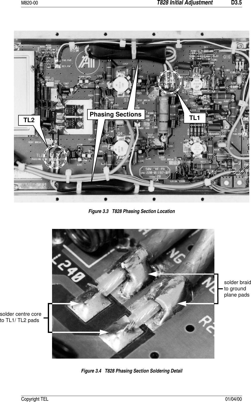
![M820-00 T828 Initial Adjustment D3.7Copyright TEL 01/04/003.5 High Temperature Shutdown Power LevelNote: The temperature shutdown circuit is factory set to approximately 130°C and20W. RV69 and RV74 should not be readjusted if normal operation isrequired.Power up the T828 and adjust the power control pot. (RV63) for the normal oper-ating power level.Turn the temperature set pot. (RV69) fully anticlockwise to avoid RF powercycling between the levels set by RV63 and RV74.Apply heat to the NTC (R300) with the tip of a soldering iron.Adjust the shutdown power level pot. (RV74) to the desired level. For continuousoperation during fault conditions, set the shutdown power in the range 10 to 20W.For normal operation, i.e. shutdown under extreme PA internal temperatures(approx. 130°C) or excessive dissipation in the splitter balance resistor (R220),adjust the temperature set pot. (RV69) for a voltage reading of 150mV at TP1 (pin12 of the LM324D [IC1]).3.6 Remote Forward Power Meter CalibrationIf a remote meter is connected, adjust the forward power meter calibration control(RV43) for the remote reading to agree with the RF power meter reading.3.7 Remote Reverse Power Meter CalibrationIf a remote meter is connected, connect a 50 ohm 3dB pad (with the output opencircuit) to the PA output.Apply RF drive and Tx key.Adjust the reverse power meter calibration control (RV57) for a quarter of the for-ward power reading.](https://usermanual.wiki/Tait/TEL0042/User-Guide-111477-Page-173.png)