Tait TEL0060 Base Station Transmitter User Manual 8c500 bk
Tait Limited Base Station Transmitter 8c500 bk
UserManual.wiki
>
Tait
>
TEL0060 User Manual
Users Information
Navigation menu
Upload a User Manual
Namespaces
Wiki Guide
HTML
PDF
Info
Views
User Manual
Discussion / Help
Navigation


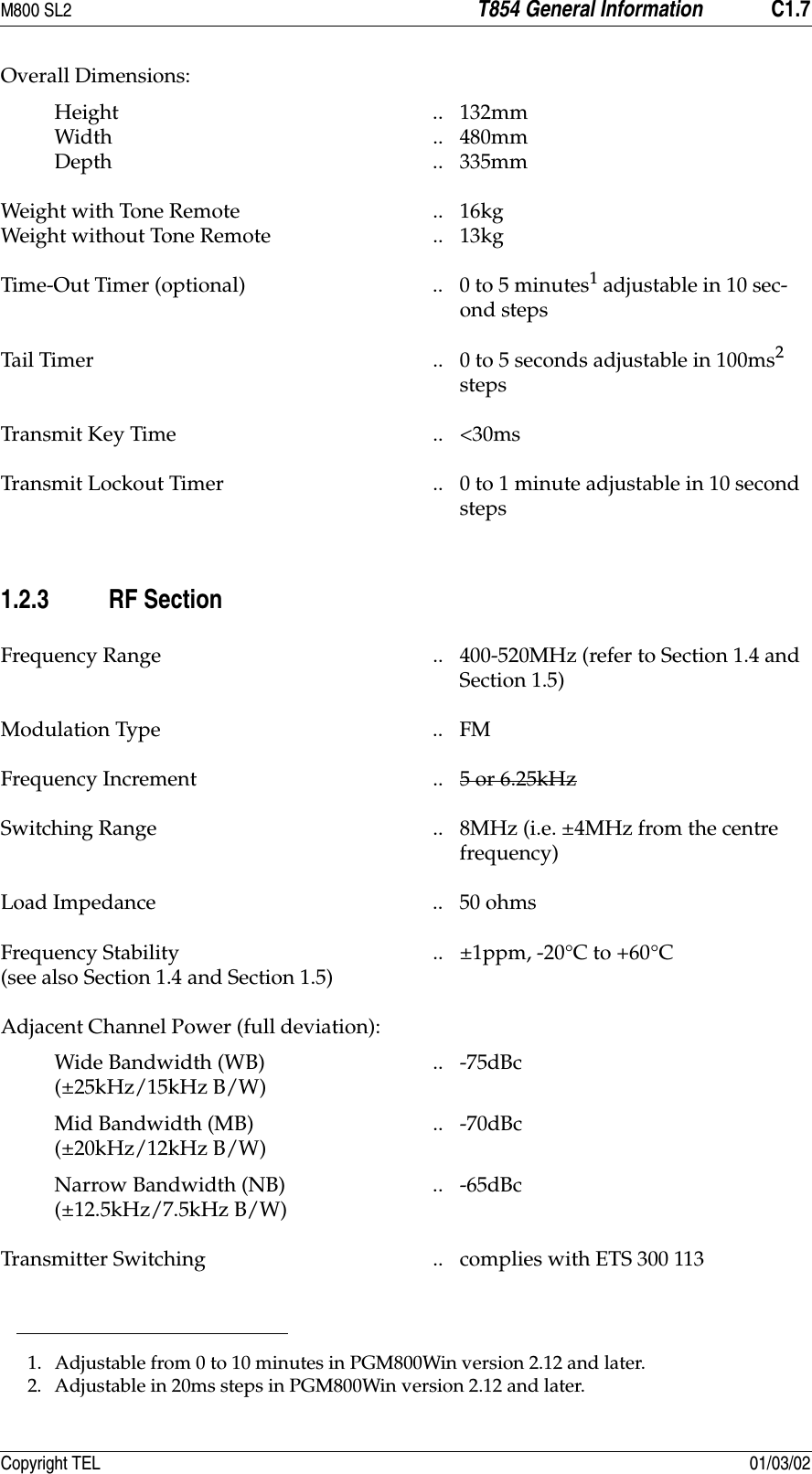
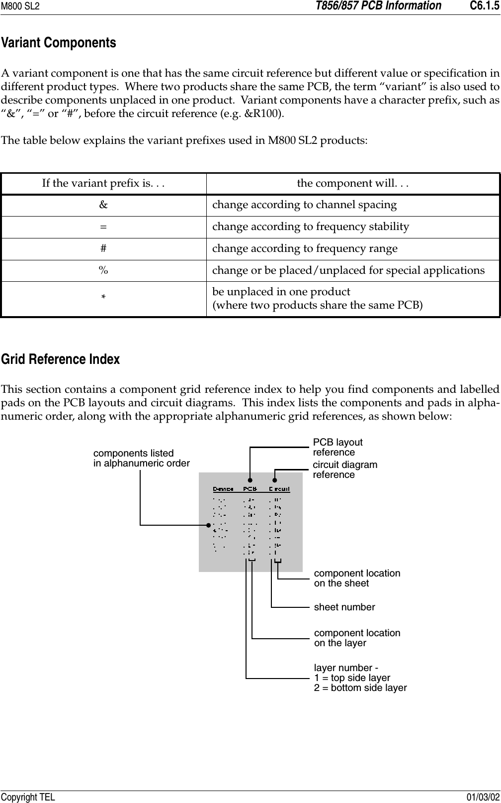
![M800 SL2 T854 General Information C1.9Copyright TEL 01/03/02Sensitivity (60% modulation @ 1kHz)- With Compressor .. -70dBm Without Compressor .. -50dBm1.2.4.2 Modulation CharacteristicsFrequency Response .. flat or pre-emphasised (optional) (below limiting)Line And Microphone Inputs: Pre-emphasised Response- Bandwidth .. 300Hz to 3kHz (WB & MB).. 300Hz to 2.55kHz (NB)Below Limiting .. within +1, -3dB of a 6dB/octavepre-emphasis characteristic Flat Response .. within +1, -2dB of output at 1kHzAbove Limiting Response .. within +1, -2dB of a flat response(ref. 1kHz)Distortion .. 2% max.Hum And Noise: Wide Bandwidth .. -55dB (300Hz to 3kHz [EIA]) typical Mid Bandwidth .. -54dB (CEPT)Narrow Bandwidth .. -50dB (CEPT) Compressor (optional): Attack Time .. 10ms Decay Time .. 800ms Range .. 50dB1.2.4.3 CTCSSStandard Tones .. all 37 EIA group A, B and C tonesplus 13 commonly used tonesFrequency Error .. 0.08% max.(from EIA tones)Generated Tone Distortion .. 1.2% max.Generated Tone Flatness .. flat across 67 to 250.3Hz to within 1dBModulation Level .. adjustableModulated Distortion .. <5%](https://usermanual.wiki/Tait/TEL0060/User-Guide-249252-Page-11.png)

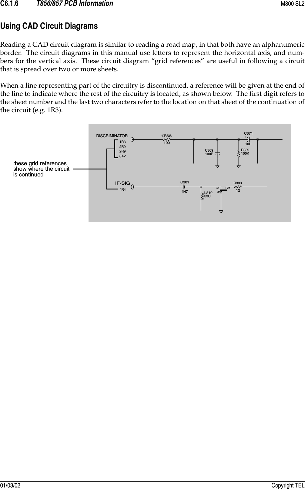
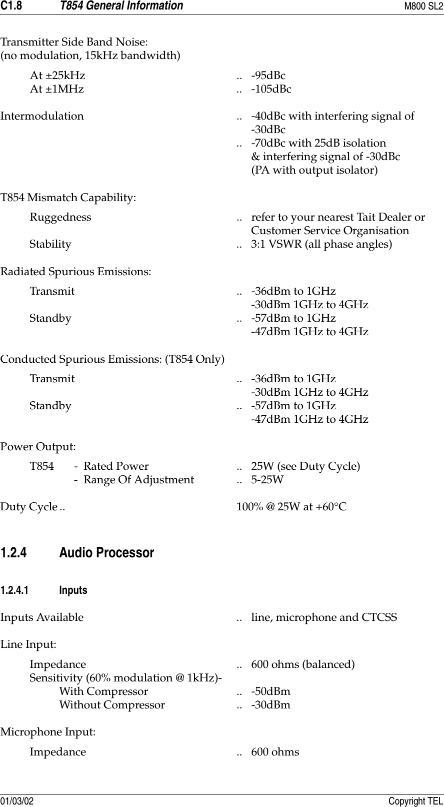
![M800 SL2 T854 Circuit Operation C2.9Copyright TEL 01/03/022.5.3 Keying InputsThere are four ways to key the exciter: •pulling the Tx-Key line low (pin 13 on D-range 1 [PL100]) at the rear of the set);•pushing the "Carrier" button on the front panel - this will inhibit all audio;•using the PTT button on the local microphone, disabling audio from the line;•via the opto-key inputs (pins 11 and 12 on D-range 1 [PL100]) when electricalisolation is required. This features a constant current sink (Q270) to ensure reli-able activation of the opto-coupler (IC250) at low keying voltages.2.5.4 Compressor (Automatic Level Control (ALC))The input signal is fed via a current controlled attenuator (Q230, Q220) to a high gainstage (IC230) from which the output signal is taken. This signal is passed to a compara-tor (IC230) which toggles whenever the audio signal exceeds a DC threshold deter-mined by RV220. Thus, the comparator produces a square wave whose mark-spaceratio is determined by the amplitude of the audio signal. This square wave pumps upthe reservoir capacitor (C233) which controls the attenuator (Q230, Q220), thus complet-ing the feedback loop.The compression level is set by adjustment of the comparator threshold (RV220).Note: Although the high dynamic range of the compressor allows the use of verylow audio signal levels, such conditions will be accompanied by a degrada-tion of the signal-to-noise ratio. Very low audio input levels should there-fore be avoided where possible.2.5.5 Outputs To ModulatorsThe output signal from the limiter (IC210, IC230) is summed with a CTCSS tone at asumming amplifier (IC260). The signal is then low pass filtered (IC260) and split to sup-ply the two modulators.Since the VCO modulator is a true frequency modulator, its audio is simply buffered(IC260). The reference modulator, however, is a phase modulator and its audio mustfirst be integrated (IC210).It is vital that the audio levels to the modulators are accurately set, relative to eachother. Hence the inclusion of level adjustment in the reference modulator path. Onceset, adjustments to absolute deviation may be made only by IC220, a 256-step 10k elec-tronic potentiometer (EPOT), which is controlled via PGM800Win. The EPOT is madeup of 256 resistive sections (representing approximately 39Ω each) which can be indi-vidually addressed by the microcontroller. Each section can be switched in or out of cir-cuit to achieve the required total resistance, thus adjusting the absolute deviation level.](https://usermanual.wiki/Tait/TEL0060/User-Guide-249252-Page-27.png)

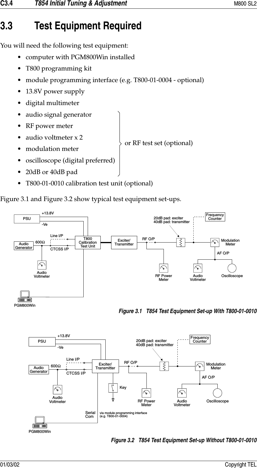
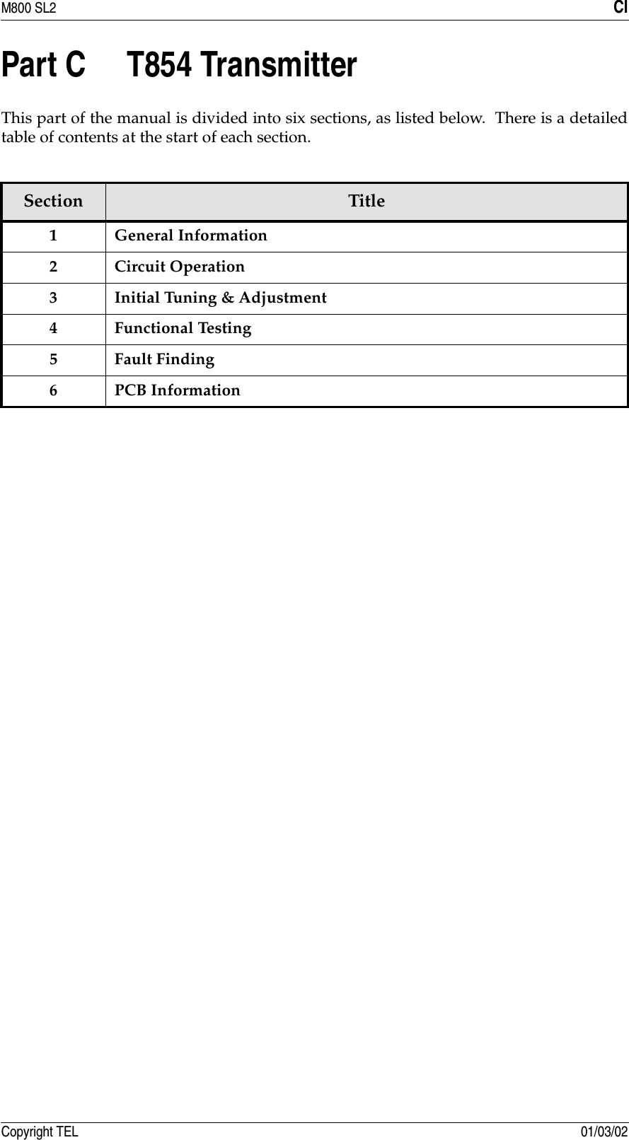
![C3.6 T854 Initial Tuning & Adjustment M800 SL201/03/02 Copyright TEL3.4.4 Two Point Modulation AdjustmentNote 1: In this and following sections deviation settings are given first for widebandwidth sets, followed by settings in brackets for mid bandwidth sets ( )and narrow bandwidth sets [ ].Note 2: The reference modulation and limiter adjustments are controlled by 256-step electronic potentiometers (EPOTs), which are adjusted via the “Refer-ence Modulation” and “Deviation” settings in PGM800Win. This allows thetwo point modulation and deviation settings to be adjusted for each chan-nel.Note 3: To optimise the modulation response across the switching range, repeatsteps 1-4 below for each channel that will be used (usually needed only fordata applications). In applications where the modulation response is lesscritical (e.g. voice use only), carry out steps 1-4 below on the middle channeland use the “EPOT Fill” option1 in PGM800Win to copy the value to theother channels.Note 4: If you are using an RF test set, turn the low pass filter off and set the highpass filter to 15kHz before beginning this procedure.1. Inject an audio signal of 300Hz 1.5V rms (+5dBm) into the CTCSS input (D-range1 (PL100) pin 8). Key the transmitter by earthing the Tx-Key line.2. Adjust the output from the audio generator to obtain ±3kHz (±2.4kHz) [±1.5kHz]deviation at 300Hz.3. Change the input frequency to 100Hz and, using PGM800Win, adjust the value ofthe “Reference Modulation” EPOT setting for the current channel to obtain ±3kHz(±2.4kHz) [±1.5kHz] deviation (you can use either the mouse or up and downarrow keys).4. Change the input frequency back to 300Hz.Repeat steps 2 and 3 above until the deviations achieved at the two input frequen-cies are within 0.2dB of each other. You will need to do this at least four times.5. Sweep the audio between 50 and 300Hz for peaks.Note: A peak between 50 and 300Hz will indicate a fault condition, i.e:- incorrect set-up or - modulation circuitry fault. The specification window is ±1dB relative to 150Hz from 67 to 260Hz.1. Use the “EDIT FILL” button on the tool bar or go to “Edit”, “Fill”, “Epot Settings” on the menu bar.](https://usermanual.wiki/Tait/TEL0060/User-Guide-249252-Page-38.png)
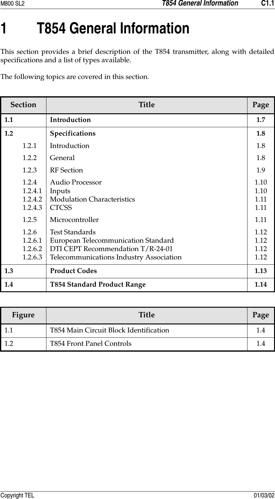
![M800 SL2 T854 Initial Tuning & Adjustment C3.7Copyright TEL 01/03/023.4.5 CTCSS Encoder (If Used)Program a CTCSS tone on the default channel using PGM800Win.If you are using an RF test set, turn off the 300Hz high pass filter.Key the T854 with the front panel "Carrier" switch.Adjust RV805 (CTCSS level adjust) to give ±500Hz (±350Hz) [±250Hz] deviation.Set the maximum deviation as per Section 3.4.6.3.4.6 FM Deviation (Limiter) AdjustmentNote: If the T854 will be used over the whole 8MHz switching range, you must setthe deviation for each channel. However, if the module will be used on fre-quencies that cover only a 1MHz (or less) switching range, you can set thedeviation on the middle channel and use this value for all other channelswith the “EPOT Fill” option in PGM800Win.Inject 1kHz at -10dBm into the line input (D-range 1 (PL100) pins 1 & 4; pins 2 & 3shorted; refer to Section 2.2 of Part F).Adjust RV210 (line sensitivity) fully clockwise and key the transmitter by earthingthe Tx-Key line. Using PGM800Win, adjust the value of the “Deviation” EPOTsetting for the current channel to obtain a deviation limit of ±4.7kHz (±3.8kHz)[±2.3kHz] (you can use either the mouse or up and down arrow keys).Sweep the audio frequency from 100Hz to 4kHz and ensure that the maximumdeviation does not exceed ±4.7kHz (±3.8kHz) [±2.3kHz]. Readjust “Deviation” ifnecessary via PGM800Win.3.4.7 Line-in Level AdjustmentRemove the CTCSS signal (if used).Set the injected signal at the line input to the required line level (typically -10 to-20dBm).Adjust RV210 (line sensitivity) to provide ±3kHz (±2.4kHz) [±1.5kHz] deviation.Reapply the CTCSS signal (if required).](https://usermanual.wiki/Tait/TEL0060/User-Guide-249252-Page-39.png)
![C3.8 T854 Initial Tuning & Adjustment M800 SL201/03/02 Copyright TEL3.5 Audio Processor Links3.5.1 Link DetailsUse the following table to set up the audio processor to the configuration you require.You should set the audio processor links before carrying out any of the tuning andadjustment procedures. The factory settings are shown in brackets [ ].3.5.2 Typical OptionsPlug Linkaa. The letters in this column and in the table in Section 3.5.2 below refer to the identificationletters screen printed onto the PCB beside each pair of pins.FunctionPL2051-2[3-4]5-6ABCnot connectedmicrophone pre-amp. output to compressor inputmicrophone pre-amp. output to multiplexer inputPL210[1-2]3-45-6LMNmultiplexer output to pre-emphasis inputmultiplexer output to limiter inputmultiplexer output to compressor inputPL2151-2[3-4]5-67-89-10GHIJKnot connectedcompressor output to multiplexer inputcompressor output to limiter inputcompressor output to pre-emphasis inputnot connectedPL2201-2[3-4]5-6DEFpre-emphasis output to multiplexer inputpre-emphasis output to limiter inputnot connectedPL205 PL210 PL215 PL220microphone pre-amp. compressedand pre-emphasised;line input pre-emphasised(standard set-up)[3-4]B[1-2]L[3-4]H[3-4]Emicrophone pre-amp. compressedand pre-emphasised;line input unprocessed3-4B3-4M7-8J1-2Dline and microphone compressedand pre-emphasised5-6C5-6N7-8J3-4Emicrophone pre-amp. compressed;line and microphone flat response3-4B3-4M3-4H5-6F](https://usermanual.wiki/Tait/TEL0060/User-Guide-249252-Page-40.png)
![M800 SL2 T854 Initial Tuning & Adjustment C3.11Copyright TEL 01/03/023.9 Audio Processor & CTCSS3.9.1 Two Point ModulationThe T854 utilise two point modulation to obtain a wide audio bandwidth independentof the synthesiser loop filter response. This is achieved by simultaneously frequencymodulating the VCO and phase modulating the synthesiser reference frequency. Therelative signal levels fed to the two modulators are quite critical and cause interactionwhen setting up.Both modulating signals require readjustment when the exciter is shifted in frequencygreater than the switching range (i.e. ∆F>±4MHz).Note 1: In this and following sections deviation settings are given first for widebandwidth sets, followed by settings in brackets for mid bandwidth sets ( )and narrow bandwidth sets [ ].Note 2: The reference modulation and limiter adjustments are controlled by 256-step electronic potentiometers (EPOTs), which are adjusted via the “Refer-ence Modulation” and “Deviation” settings in PGM800Win. This allows thetwo point modulation and deviation settings to be adjusted for each chan-nel.Note 3: To optimise the modulation response across the switching range, repeatsteps 1-4 below for each channel that will be used (usually needed only fordata applications). In applications where the modulation response is lesscritical (e.g. voice use only), carry out steps 1-4 below on the middle channeland use the “EPOT Fill” option1 in PGM800Win to copy the value to theother channels.Note 4: If you are using an RF test set, turn the low pass filter off and set the highpass filter to 15kHz before beginning this procedure.3.9.2 Modulator Adjustment1. Inject an audio signal of 300Hz 1.5V rms (+5dBm) into the CTCSS input (D-range1 (PL100) pin 8). Key the transmitter by earthing the Tx-Key line.2. Adjust the output from the audio generator to obtain ±3kHz (±2.4kHz) [±1.5kHz]deviation at 300Hz.3. Change the input frequency to 100Hz and, using PGM800Win, adjust the value ofthe “Reference Modulation” EPOT setting for the current channel to obtain ±3kHz(±2.4kHz) [±1.5kHz] deviation (you can use either the mouse or up and downarrow keys).1. Use the “EDIT FILL” button on the tool bar or go to “Edit”, “Fill”, “Epot Settings” on the menu bar.](https://usermanual.wiki/Tait/TEL0060/User-Guide-249252-Page-43.png)
![C3.12 T854 Initial Tuning & Adjustment M800 SL201/03/02 Copyright TEL4. Change the input frequency back to 300Hz.Repeat steps 2 and 3 above until the deviations achieved at the two input frequen-cies are within 0.2dB of each other. You will need to do this at least four times.5. Sweep the audio between 50 and 300Hz for peaks.Note: A peak between 50 and 300Hz will indicate a fault condition, i.e:- incorrect set-up or - modulation circuitry fault. The specification window is ±1dB relative to 150Hz from 67 to 260Hz.3.9.3 CTCSS Encoder (If Used)Program a CTCSS tone on the default channel using PGM800Win.If you are using an RF test set, turn off the 300Hz high pass filter.Key the T854 with the front panel "Carrier" switch.Adjust RV805 (CTCSS level adjust) to give ±500Hz (±350Hz) [±250Hz] deviation.Set the maximum deviation as per Section 3.9.4.3.9.4 Limiter AdjustmentNote: If the T854 will be used over the whole 8MHz switching range, you must setthe deviation for each channel. However, if the module will be used on fre-quencies that cover only a 1MHz (or less) switching range, you can set thedeviation on the middle channel and use this value for all other channelswith the “EPOT Fill” option in PGM800Win.Set the links in the audio processor section as required (refer to Section 3.5).Inject 1kHz at -10dBm into the line input (D-range 1 (PL100) pins 1 & 4; and pins 2& 3 shorted; refer to Section 2.2 of Part F).Adjust RV210 (line sensitivity) fully clockwise and key the transmitter by earthingthe Tx-Key line. Using PGM800Win, adjust the value of the “Deviation” EPOTsetting for the current channel to obtain a deviation limit of ±4.7kHz (±3.8kHz)[±2.3kHz] (you can use either the mouse or up and down arrow keys).Sweep the audio frequency from 100Hz to 4kHz and ensure that the maximumdeviation does not exceed ±4.7kHz (±3.8kHz) [±2.3kHz]. Readjust “Deviation” ifnecessary via PGM800Win.](https://usermanual.wiki/Tait/TEL0060/User-Guide-249252-Page-44.png)
![M800 SL2 T854 Initial Tuning & Adjustment C3.13Copyright TEL 01/03/023.9.5 Line Level Without CompressorThis section assumes that the compressor is not used. If the compressor is required,refer to Section 3.9.6.Remove the CTCSS signal (if used).Adjust the line sensitivity as follows: •set the injected signal at the line input to the required line level (typically -10 to-20dBm);•adjust RV210 (line sensitivity) to provide ±3kHz (±2.4kHz) [±1.5kHz] devia-tion.Reapply the CTCSS signal (if required).3.9.6 CompressorThe compressor may be used on the line input only, the microphone input only, or onboth the line and microphone inputs. If the compressor is used, refer to one of the fol-lowing sections as appropriate.3.9.6.1 Compressor On Line Input OnlySet RV210 (line sensitivity) fully clockwise and key the transmitter by earthing theTx-Key line.Reduce the line level to -50dBm at 1kHz and set RV220 (compression level) fullyclockwise.Check that ±3kHz deviation (±2.4kHz) [±1.5kHz] is still available.Slowly increase the audio input level until the demodulated waveform shows sig-nificant signs of clipping (approximately ±4.5kHz (±3.6kHz) [±2.3kHz] deviation).Adjust RV220 anticlockwise until the demodulated waveform is just clipping(approximately ±4kHz (±3.2kHz) [±2kHz] deviation).Increase the input level to -10dBm and check that the test tone is still held just intoclipping. The input line level should be typically -10 to -20dBm.3.9.6.2 Compressor On Microphone Input OnlyKey the transmitter by earthing the Tx-Key line and plug a microphone jack intothe front panel socket.Adjust RV220 (compression level) fully clockwise.Acoustically couple the microphone to a tone box (1kHz) and close the PTTswitch.](https://usermanual.wiki/Tait/TEL0060/User-Guide-249252-Page-45.png)
![C3.14 T854 Initial Tuning & Adjustment M800 SL201/03/02 Copyright TELIncrease the audio level until the demodulated waveform shows significant signsof clipping (approximately ±4.5kHz (±3.6kHz) [±2.3kHz] deviation).Adjust RV220 anticlockwise until the demodulated waveform is just clipping(approximately ±4kHz (±3.2khz) [±2kHz] deviation).Increase the audio level by 10dB and verify that the test tone is held just into clip-ping.Whistle steadily into the microphone, checking that approximately ±4kHz(±3.2khz) [±2kHz] deviation is produced. The modulated waveform should bebasically sinusoidal.Speak into the microphone, checking that the modulation peaks reach about±5kHz (±4kHz) [±2.5kHz] deviation.As the line is to be used without compression, set RV210 (line sensitivity) asdescribed in Section 3.9.5.3.9.6.3 Compressor On Both Line & Microphone InputsSet up as described in Section 3.9.6.1.](https://usermanual.wiki/Tait/TEL0060/User-Guide-249252-Page-46.png)
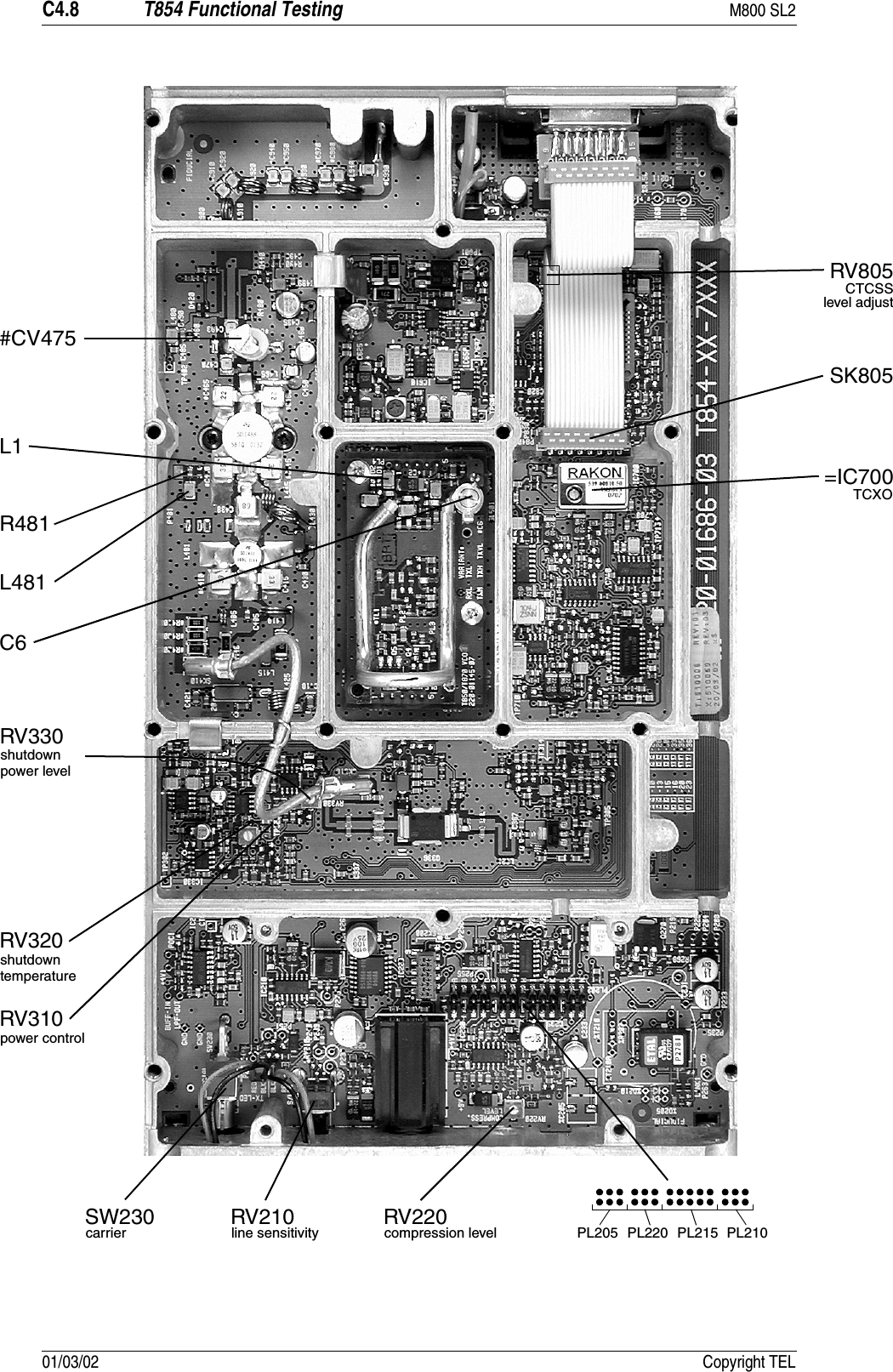
![M800 SL2 T854 Functional Testing C4.1Copyright TEL 01/03/024 T854 Functional TestingCaution: This equipment contains CMOS devices which are susceptible to dam-age from static charges. Refer to Section 1.2 in Part A for more infor-mation on anti-static procedures when handling these devices.The following test procedures will confirm that the T854 has been tuned and adjustedcorrectly and is fully operational.Note 1: In this and following sections deviation settings are given first for widebandwidth sets, followed by settings in brackets for mid bandwidth sets ( )and narrow bandwidth sets [ ].Note 2: Unless otherwise specified, the term "PGM800Win" used in this and follow-ing sections refers to version 3.00 and later of the software.Refer to Figure 4.4 and Figure 4.5 for the location of the main tuning and adjustmentcontrols, and to Section 3.3 for the test equipment set-up. Refer also to Section 6 wherethe parts lists, grid reference index and diagrams will provide detailed information onidentifying and locating components and test points on the main PCB. The parts listand diagrams for the VCO PCB are in Part E.The following topics are covered in this section.Section Title Page4.1 Current Consumption 4.34.2 Output Power 4.34.3 Output Frequency 4.34.4 Timers 4.34.5 Frequency Response 4.44.6 Audio Level Input Sensitivity 4.7Figure Title Page4.14.24.34.44.5T854 Transmit TimersT854 Pre-emphasis ResponseT854 Limiting ResponseT854 Main Tuning & Adjustment ControlsT857 Main Tuning & Adjustment Controls4.44.54.64.94.11](https://usermanual.wiki/Tait/TEL0060/User-Guide-249252-Page-47.png)

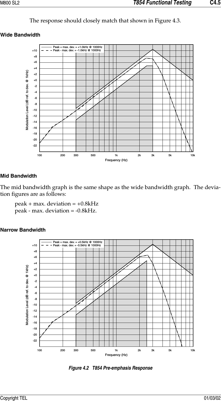
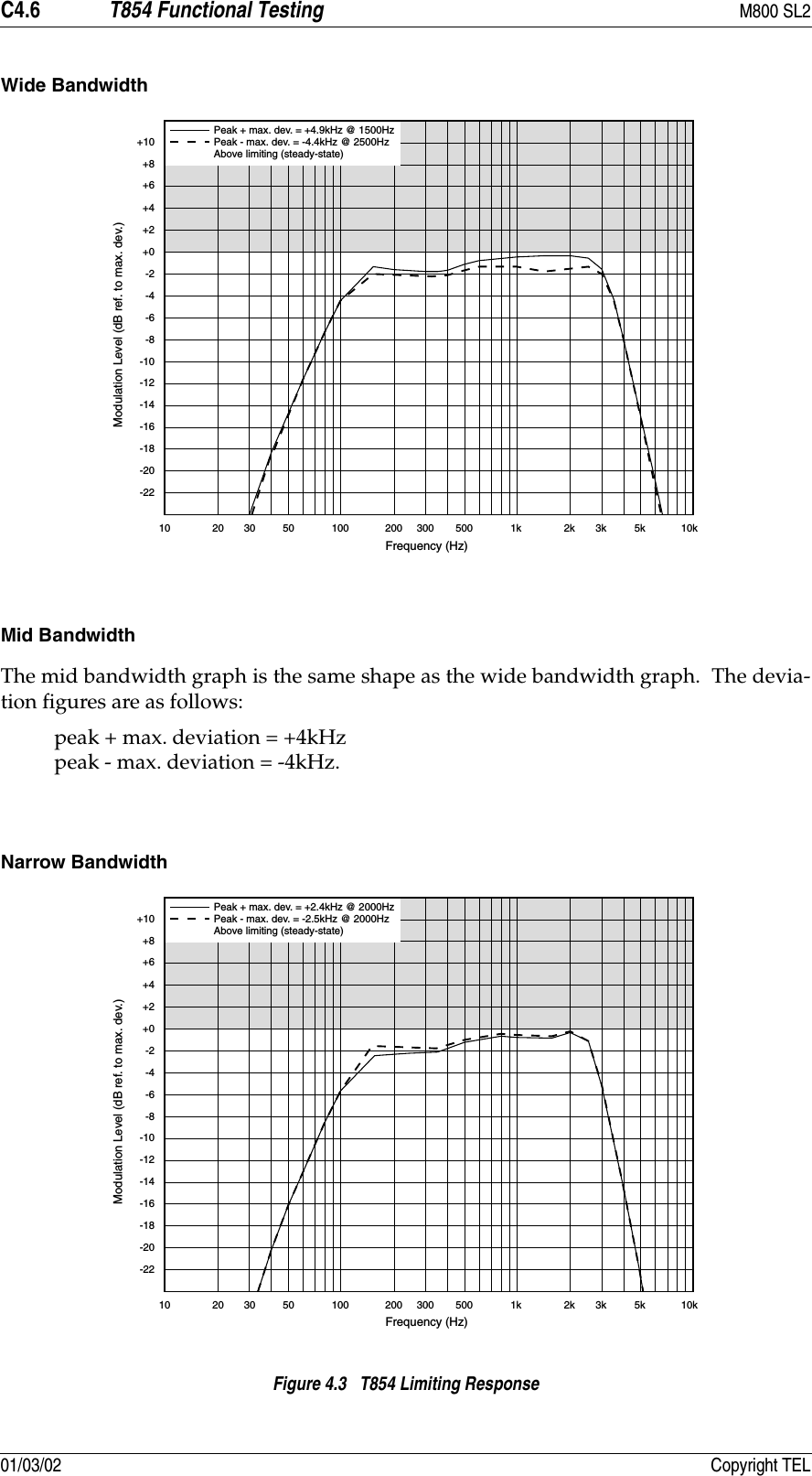
![C4.4 T854 Functional Testing M800 SL201/03/02 Copyright TELFigure 4.1 T854 Transmit Timers4.5 Frequency ResponseIf the T854 has been correctly adjusted, the pre-emphasis and limiting responses shouldclosely match those shown in Figure 4.2 and Figure 4.3 respectively. Note: The limits shown on these graphs should not be exceeded. •If you are using an RF test set, turn off all filters.•Measure the pre-emphasis response as follows: Reduce the line level to give ±1kHz (±0.8kHz) [±0.5kHz] deviation at 1kHz. Sweep the modulation frequency. The response should closely match that shown in Figure 4.2.•Measure the limiting response as follows: Set the line level to give ±3kHz (±2.4kHz) [±1.5kHz] deviation at 1kHz. Increase the line level 20dB and sweep the modulation frequency. Transmit Tail Sets the tail time during which the transmitter stays keyed after the exter-nal key source has been removed.0-5 seconds in 100ms stepsaTransmit Timeout Sets the maximum continuous trans-mission time. Once the timer has timed out, the transmitter must be keyed again, unless prevented by the transmit lockout timer.0-300 secondsb in 10 second stepsTransmit Lockout Sets the period of time that must elapse after a timeout before the trans-mitter can re-transmit. Once the timer has timed out, the transmitter can be keyed again.0-60 seconds in 10 second stepsa. Adjustable in 20ms steps in PGM800Win version 2.12 and later.b. Adjustable in 20ms steps in PGM800Win version 2.12 and later.OnLockout TimeTimeoutTimeOnTail TimeTx-EnableTx-Reg.Tx-EnableTx-Reg.](https://usermanual.wiki/Tait/TEL0060/User-Guide-249252-Page-50.png)
![M800 SL2 T854 Functional Testing C4.7Copyright TEL 01/03/024.6 Audio Level Input Sensitivity•Adjust RV210 (line sensitivity) fully clockwise.•Check that the input sensitivities are better than those specified below:Note: A degraded signal to noise ratio can be expected with the compressorselected. The extent of the degradation is dependent on the audio inputlevel.Line Input 600 ohms, ±3kHz (±2.4kHz) [±1.5kHz] deviation at 1kHz: with compressor -50dBm without compressor -30dBmMicrophone Input 600 ohms, ±3kHz (±2.4kHz) [±1.5kHz] deviation at 1kHz: with compressor -75dBm without compressor -55dBmCTCSS Input 1kHz deviation at 150Hz 500mV rms](https://usermanual.wiki/Tait/TEL0060/User-Guide-249252-Page-53.png)
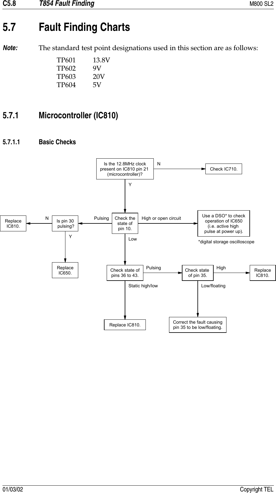
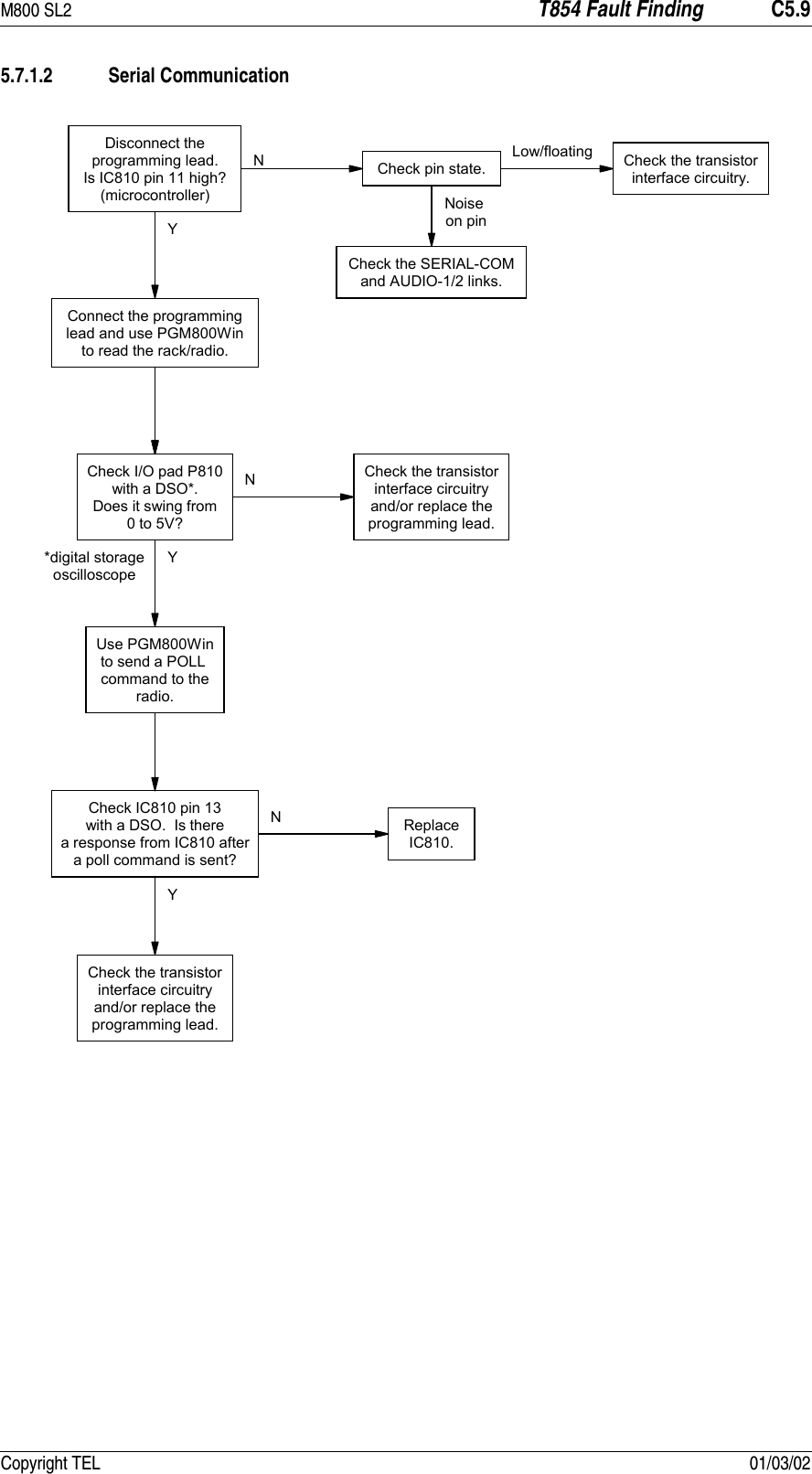
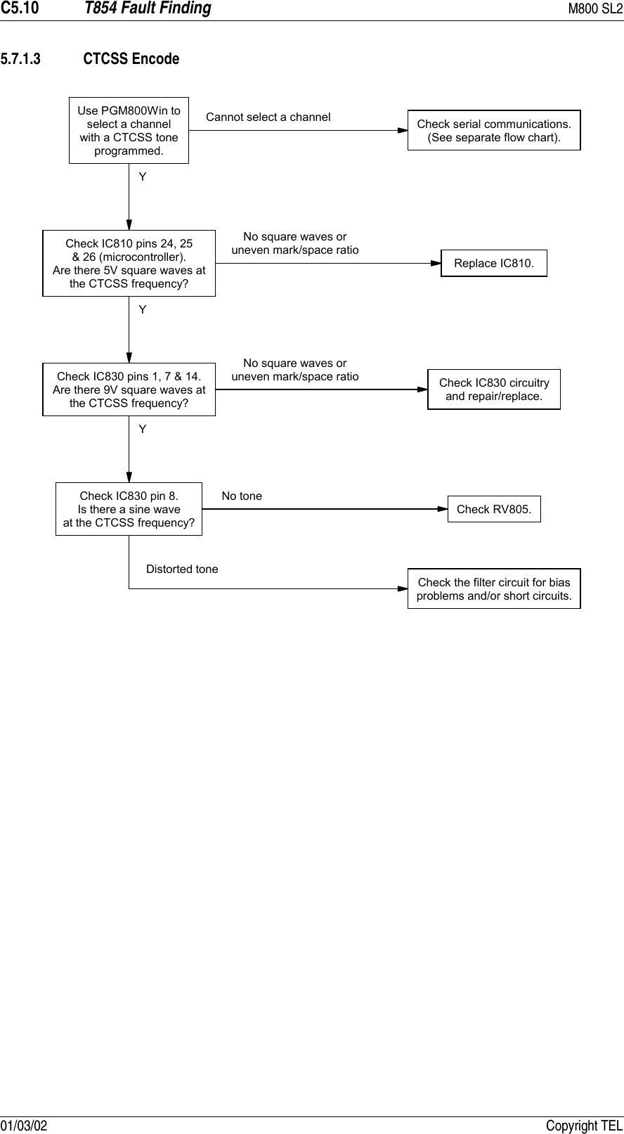
![M800 SL2 T854 Fault Finding C5.1Copyright TEL 01/03/025 T854 Fault FindingCaution: This equipment contains CMOS devices which are susceptible to dam-age from static charges. Refer to Section 1.2 in Part A for more infor-mation on anti-static procedures when handling these devices.The following test procedures and fault finding flow charts may be used to help locate ahardware problem, however they are by no means a complete fault finding procedure.If you still cannot trace the fault after progressing through them in a logical manner,contact your nearest Tait Dealer or Customer Service Organisation. If necessary, youcan get additional technical help from Customer Support, Radio Systems Division, TaitElectronics Ltd, Christchurch, New Zealand (full contact details are on page 2).Note 1: In this and following sections deviation settings are given first for widebandwidth sets, followed by settings in brackets for mid bandwidth sets ( )and narrow bandwidth sets [ ].Note 2: Unless otherwise specified, the term "PGM800Win" used in this and follow-ing sections refers to version 3.00 and later of the software.Refer to Section 6 where the parts lists, grid reference index and diagrams will providedetailed information on identifying and locating components and test points on themain PCB. The parts list and diagrams for the VCO PCB are in Part E.The following topics are covered in this sectionSection Title Page5.1 Visual Checks 5.35.2 Component Checks 5.35.3 Front Panel LED Indicator 5.35.45.4.15.4.2DC ChecksPower RailsVCO Locking5.45.45.45.55.5.15.5.25.5.35.5.4RF ChecksT854 Drive PowerT854 PA Output PowerT857 Output PowerAudio And Modulation5.55.55.55.55.65.6 PGM800Win Generated Errors 5.7](https://usermanual.wiki/Tait/TEL0060/User-Guide-249252-Page-55.png)
![C5.6 T854 Fault Finding M800 SL201/03/02 Copyright TELCheck that the demodulated RF output has the frequency response referred to inSection 4.5 with at least ±5kHz (±4kHz) [±2.5kHz] deviation available at 1kHzmodulating frequency.If the above result is not achieved, either the two modulators are incorrectly adjusted ora fault condition exists.](https://usermanual.wiki/Tait/TEL0060/User-Guide-249252-Page-60.png)