Technalogix TAV1000L VHF TELEVISION BROADCAST AMPLIFIER User Manual TAV 1000
Technalogix, Ltd. VHF TELEVISION BROADCAST AMPLIFIER TAV 1000
USERS MANUAL

TAV-1000
POWER AMPLIFIER
NEW
ADVENTURES
IN
BROADCASTING
Technalogix
You’ve already unpacked it, haven’t you? You’ve unpacked it and
plugged it in and turned it on and fiddled with the knobs. No?
Okay, good. Please take a few minutes to read the manual and
familiarize yourself with your new Technalogix power amplifier.
We believe that this manual, and of course our equipment, should
be everything you need to get on the air with superb broadcast
quality video. We understand that a capable and confident user
will get the most out of our product and we have made every
attempt to educate readers of all technical levels. If there is
something that is not clear, or you require further information,
please do not hesitate to contact us and we’ll be glad to help out.
Technalogix Ltd.
#4, 8021 Edgar Industrial Place
Red Deer, Alberta, Canada
T4P 3R3
Phone: 403.347.5400
Fax: 403.347.7444
URL: www.technalogix.ca
Email: technical@technalogix.ca
sales@technalogix.ca
We truly appreciate that you have chosen us as your television
broadcast system supplier. Happy viewing.
Table of Contents
SECTION I- SAFEGUARDS ..............................................................................................I-1
SAFETY AND FIRST AID.....................................................................................................I-2
OPERATING SAFEGUARDS................................................................................................I-3
SECTION II - WARRANTY.............................................................................................II-1
SECTION III - OVERVIEW..............................................................................................III-1
STANDARD FEATURES....................................................................................................III-1
PRINCIPLE OF OPERATION..............................................................................................III-2
BLOCK DIAGRAM (TAV-1000).......................................................................................III-3
BLOCK DIAGRAM (TAV-500) .........................................................................................III-6
BLOCK DIAGRAM (COMBINER/FILTER ENCLOSURE)......................................................III-8
SPECIFICATIONS .............................................................................................................III-9
SECTION IV - RF COMPONENTS.................................................................................IV-1
AMPLIFIER PALLETS........................................................................................................IV-1
SPLITTER/COMBINER......................................................................................................IV-4
FINAL COMBINER............................................................................................................IV-5
DIRECTIONAL COUPLER..................................................................................................IV-5
FILTER.............................................................................................................................IV-5
SECTION V - POWER SUPPLY SECTION...................................................................... V-1
SECTION VI - MONITOR AND CONTROL SYSTEM........................................................VI-1
CONTROL BOARD OVERVIEW (SERIES II REV I)............................................................VI-1
POWER SUPPLY COMPONENTS......................................................................................VI-1
INTERFACE COMPONENTS..............................................................................................VI-2
SIGNAL CONDITIONING COMPONENTS...........................................................................VI-3
DISPLAY COMPONENTS ..................................................................................................VI-4
MICROCONTROLLER COMPONENTS ...............................................................................VI-5
FAULT SHUTDOWN..........................................................................................................VI-6
ENCLOSURE INTERFACING..............................................................................................VI-7
REMOTE PORT................................................................................................................VI-7
BILL OF MATERIALS........................................................................................................VI-7
SCHEMATICS ...................................................................................................................VI-7
SECTION VII - MECHANICAL SECTION...................................................................... VII-1
SECTION VIII - INSTALLATION.................................................................................. VIII-1
BUILDING RECOMMENDATIONS ................................................................................... VIII-1
HEATING AND COOLING REQUIREMENTS.................................................................... VIII-2
ELECTRICAL SERVICE RECOMMENDATIONS................................................................ VIII-3
ANTENNA AND TOWER RECOMMENDATIONS............................................................... VIII-4
SHELTER SECURITY..................................................................................................... VIII-5
UNPACKING AND INSPECTION...................................................................................... VIII-6
LOCATION AND FUNCTION OF CONTROLS AND CONNECTORS (TAV-500 POWER
AMPLIFIERS)................................................................................................................. VIII-7
LOCATION AND FUNCTION OF CONTROLS AND CONNECTORS (COMBINER/FILTER
ENCLOSURE)................................................................................................................ VIII-9
INITIAL HOOK UP........................................................................................................VIII-11
SECTION IX - OPERATING PROCEDURES....................................................................IX-1
SECTION X - MAINTENANCE AND TROUBLESHOOTING............................................... X-1
TROUBLESHOOTING........................................................................................................ X-2
I-1
Section I - Safeguards
General Safeguards
This section is written as a general guide to keep all 5 fingers on your hand and is intended for those
having previous knowledge and experience with these kinds of equipment. It is not intended to
contain a complete statement of all safety precautions, which should be observed by personnel using
this or other electronic equipment.
DOCUMENTATION - Read, retain and follow instructions before operating the equipment.
There is a lot of useful information in the manual, and besides, we spent a lot of time
writing it!
ENVIRONMENT - To reduce the risk of fire or electric shock, do not expose this equipment
to rain, moisture, or rye and sodas at the company Christmas party. Refer all servicing to
qualified service personnel.
SERVICING - Do not attempt to service this equipment yourself as opening or removing
covers can result in a warm tingly feeling and will void the warranty. Refer all servicing to
qualified service personnel.

I-2
Safety and First Aid
Personnel engaged in the installation, operation, maintenance, or servicing of electronic equipment
are exposed to the hazard of high voltage. It is imperative that all safety regulations and precautions
are consistently observed. Knowledge of first aid procedures is recommended. The following
information is presented as a reference only.
• At all times, avoid placing any part of the body in series between ground and circuit points,
whether power is on or off.
• Dangerous voltage may be present in equipment even though power is off. Do not open the
cabinet. Refer servicing to qualified service personnel.
• It is the duty of all personnel to be prepared to give adequate emergency first aid treatment and
thereby prevent avoidable loss of life.
• There are three principle degrees of burns, recognizable as follows:
• a first-degree burn reddens the skin.
• a second-degree burn blisters the skin.
• a third degree burn chars the flesh and frequently places the victim in a state of shock
accompanied by respiratory paralysis.
• Respiratory paralysis can cause death by suffocation within seconds. It is imperative that the
approved methods of artificial respiration are initiated immediately and continue until the victim’s
breathing is normal.
• A muscular spasm of unconsciousness may render the victim unable to break free of the electric
power. If this is the case, turn the power off immediately.
DO NOT TOUCH THE VICTIM OR YOU MAY SHARE THE SAME
PREDICAMENT.
• If the power cannot be turned off immediately, very carefully loop a dry rope, article of clothing,
length of strong cloth or a rolled-up newspaper around the victim and pull the victim free of the
power source. Carefully avoid touching the victim or clothing.
• Once free of the power source, the victim must be placed in a reclining position and covered
with a blanket or newspapers to keep warm. At the first opportunity, enlist help in
summoning a doctor. If a doctor cannot be summoned, transport the victim to the doctor or a
hospital. Be sure the victim is kept well covered and warm while awaiting professional
treatment.

I-3
Operating Safeguards
It is a known fact that our broadcast transmitters and translators enjoy 50-ohm load impedances.
So much so, that it is imperative you maintain 50-ohm impedances throughout your system. In
return, your equipment will provide you with maximum power transfer to the antenna and
decreased reflected power heading back towards the amplifier pallets, reducing the amount of
magic smoke that gets let out of the power amplifier. Before anything is turned on, ensure that
there is a 50-ohm path from the output of each stage to the input of the next, all the way to the
antenna.
In addition to maintaining proper 50-ohm impedances throughout the signal chain, it is also
important, whenever possible, to make sure the RF drive going to the input of the power amplifier
is removed before turning on or turning off the DC power supply. This is because all of the RF
transistors used in the individual amplifier pallets are fabricated with LDMOS (Laterally Diffused
Metal Oxide Semiconductor) technology. Nice and linear yes, but they do not like to make any RF
power when their supply voltages are not within a specific range. When you first turn your power
amplifier on or off, the DC power supply’s output voltage may take a while to stable out to a safe
operating voltage. Ten seconds wait before applying the RF drive will ensure no issues arise.
Our power amplifiers are designed to reliably generate a specific RF output power. Failing to
adhere to overdriven amplifier warnings can decrease the reliability of your system, and frankly,
makes our repair department busy and grumpy. If you need to transmit to a little larger coverage,
you are better off increasing antenna gain, and more importantly, antenna height above average
terrain. On TV and FM broadcast frequencies, insufficient antenna height puts an upper limit on
your range, regardless of power levels, as the distance from your antenna to the radio horizon is
limited.

II-1
Section II - Warranty
Our legalese is straightforward. It is simply designed to give you peace of mind and helps you resist the
temptation to have your electronics friend try to repair your Technalogix product.
Technalogix Ltd. products have been completely tested and found to meet specifications and be in
proper operating condition. They are warranted to be free from defects in materials and workmanship
for a period of one year from the date of shipment. If the system becomes damaged in shipment and
there are obvious signs of damage to the outside of the packaging, notify your courier immediately
before that courier walks out the door.
Technalogix Ltd. will not be liable for damages of whatever nature arising out of or in connection with
the equipment or its use thereof. Technalogix does not assume responsibility for injury or damage
resulting from the practices of untrained or unqualified personnel in the handling of this equipment.
Technalogix Ltd. warranty does not include:
• misuse, neglect or accident.
• incorrect wiring and /or improper installation.
• unauthorized repairs, modifications or use in violation of instructions issued by Technalogix.
• incidental or consequential damages as a result of any defect.
• reshipment cost or insurance of the unit or replacement units or parts.
• acts of nature or terrorism.
Technalogix agrees, at our option, to remedy warranted defects or furnish a new part in exchange for
any part of a unit which, under normal installation, use and service, becomes defective. The user will
pay for transportation costs to and from the repair center.

II-2
To claim your rights under this warranty:
• Contact Technalogix and describe the problem in as much detail as possible. See troubleshooting
section in this manual. If a solution cannot be found at this time, it may be determined that the unit
will have to be returned to Technalogix for repair, once a Return Materials Authorization (RMA)
number is provided. Please look under our web site (www.technalogix.ca) for the RMA form
(Service) and fill it out. Either fax it to us or email to us.
• Package equipment carefully for prepaid shipment to Technalogix. Include a written description of
the problem experienced, a copy of the original invoice establishing warranty status, and the RMA.
Technalogix reserves the right to make revisions in current production of the equipment and assumes
no obligation to incorporate these changes in earlier models.
Shipping Address:
Technalogix Ltd.
ATTN: RMA#
#4, 8021 Edgar Industrial Place
Red Deer, Alberta, Canada
T4P 3R3
Ph: 403.347.5400
Made in Canada, returned for repairs

III-1
Section III - Overview
Standard Features
• Narrow output bandpass filter allows adjacent channel operation
• Front panel Liquid Crystal Display (LCD) to monitor forward and reflected RF power, and DC
voltage
• Microcontroller-based monitoring and control ensures amplifier will never be overdriven and high
VSWR will not damage amplifier
• AC circuit breaker on back panel to eliminate replacement of fuses
• All aluminium enclosure maintains power amplifier’s light weight
• Simple design using commonly available parts ensures reliable operation
• Predominate and third-order intermodulation distortion exceeds Industry Canada and FCC
specification.

III-2
Principle of Operation
The TAV-1000 power amplifier supplies a 1000-watt peak video signal with 10% aural power on any of
the VHF television channels 2 through 13. Please note that channel selection must be made at time of
order, as the transmitter or translator is calibrated and tested to the channel requested and is not field
tuneable. The TAV-1000 power amplifier is a modular solid-state 1000-watt broadcast amplifier utilizing
readily available RF components wherever possible, thus enhancing the serviceability of the
equipment. The TAV-1000 features ultra linear amplification and individual channel RF output
bandpass filtering. The amplifier modules are stable for high reliability and long service life.
The amplification of the TAV-1000 is comprised of (2) TAV-500 500-watt power amplifiers. Firstly, the
output of the modulator or processor gets split into (2) RF signals of equal amplitude. Each output of
the 2-way power divider is then fed into a TAV-500 Power Amplifier. Finally, the outputs of each TAV-
500 are combined to generate 1000-watts of peak visual power in addition to an aural carrier, as seen
in the TAV-1000 block diagram.
TO WATTMETER
AND ANTENNA
RF OUT
TAV-500
COMBINER
FILTER
TAV-500
SPLITTER
2-WAY
MODULATOR/PROCESSOR
POWER SUPPLY
TAV-1000 Overall Block Diagram
Date: May 25, 2005 Page: 1 of 1
Rev ID

III-4
Inside each 500-watt power amplifier, the RF signal enters through the RF Input connector on the
power amplifier enclosure from the modulator or processor. It then passes through an RF
attenuator to limit the output power level of the power amplifier and to help buffer any transients
that may come into the power amplifier. After attenuation, the signal gets preamplified by a driver
pallet before the signal gets split into (2) signals for final amplification. The output of the (2) final
amplifier pallets are combined. Finally, the signal gets filtered with a Bandpass filter and monitored
with a dual directional coupler before heading out to an antenna for broadcast.
A=-0.08dB typ.
GAIN
COMPENSATION
i
A=-0.05dB typ.
A=40dB typical
A=18dB minimum, 19dB typical
A=18dB minimum, 19dB typical
A=-0.08dB typ.
RF INPUT RF OUT
PA25-VHF DRIVER
SPLITTER
2-WAY P400-VHF FINAL
P400-VHF FINAL
2-WAY
COMBINER
VV
DIRECTIONAL COUPLER
FILTER
TAV-500 Block Diagram
Date: May 24, 2005 Page: 1 of 1
Rev ID

III-6
After amplification, the signal exits the power amplifier enclosure and goes into the combiner/filter
enclosure, where the signals from each 500-watt amplifier are combined. After combining, the
amplified signals are filtered with a bandpass filter and monitored again with another directional
coupler before heading out to an antenna for broadcast, as depicted in the following combiner
block diagram.
A=-0.6dB to -1.0dB
A=-0.05dB
A=-0.45dB
TO WATTMETER
AND ANTENNA
RF OUT
PA2 OUT
PA1 OUT
2-WAY
COMBINER
VV
COUPLERDIRECTIONAL
FILTER
TAV-1000 Combiner Enclosure Block Diagram
Date: May 25, 2005 Page: 1 of 1
Rev ID

III-8
Specifications
The following specifications were taken with a Technalogix modulator/processor. Should a different
modulator or processor be used, specifications could vary. For this reason, we recommend that any
different modulator/processor be shipped to Technalogix so the system can be matched and set up
optimally. In addition, the audio/video ratio the input to the power amplifier needs to be –10 dB in order
for the software and LCD readout to be accurate. All specifications below were taken with the
audio/video ratio set -10dB.
RF Characteristics
Frequency range any specified VHF Channel 2 to 13
Frequency Response (one channel) ±0.5 dB
Frequency Stability ±250 Hz
Selectivity 60 dB (adjacent channel)
Minimum Input Level 0 dBmV
Rated Visual Output Power 1000 Watts
Rated Aural Output Power 10% of peak visual power
IF Output Level -12 dBm nominal
Input Impedance 75 Ohms
Output Impedance 50 Ohms
Harmonics > 60 dB below rated power
Predominant Intermodulation Distortion dBc = decibels below visual carrier
+ 920 kHz
> -53 dBc
- 920 kHz
> -53 dBc
+ 2.66 MHz
> -53 dBc
- 2.66 MHz
> -53 dBc
+ 5.42 MHz
> -53 dBc
+ 7.16 MHz
> -53 dBc
3rd Order Intermodulation Distortion
- 4.5 MHz
> -60 dBc
+ 9.0 MHz
> -60 dBc
All others
> -60 dBc
Spurious Emissions > -60 dBc
NTSC Video Characteristics
Input Level to modulator (for 87.5% modulation) 1.0 VPP (100IRE + 40IRE sync)
Differential Phase (at 87.5% modulation) ±2 Degrees
Differential Gain (at 87.5% modulation) 2%
Group Delay < ±40 nS
Video Group Delay Pre-emphasis Conforms to IC/FCC specifications
K-Factor 1.9% for 2T Pulse
Hum and Noise > 60 dB below rated power
Aural Characteristics

III-9
Input Level for 25 kHz Deviation 0.3 VPP
Frequency Response (Standard Pre-emphasis) ±1 dB
Harmonic Distortion (25 kHz Deviation) < 1% 50 Hz to 15 kHz
Amplitude Modulation Noise > 50 dB
Frequency Modulation Noise > 60 dB
Intercarrier Stability ±250 Hz
Physical Characteristics
Power Requirements
Power Supply 230 VAC, 30 AAC
Combiner / Filter
115 VAC, 2 AAC
Operating Temperature Range 0°C to 50°C
Dimensions
TAV-500 Power Amplifier (each) W-19" flange (17” encl.) , D-25", H-8 3/4” (5U)
Combiner / Filter W-19" flange (17” encl.) , D-25", H-8 3/4” (5U)
Power Supply W-19” flange (17” encl.) , D-25”, H-7” (4U)

IV-1
Section IV – RF Components
Amplifier Pallets
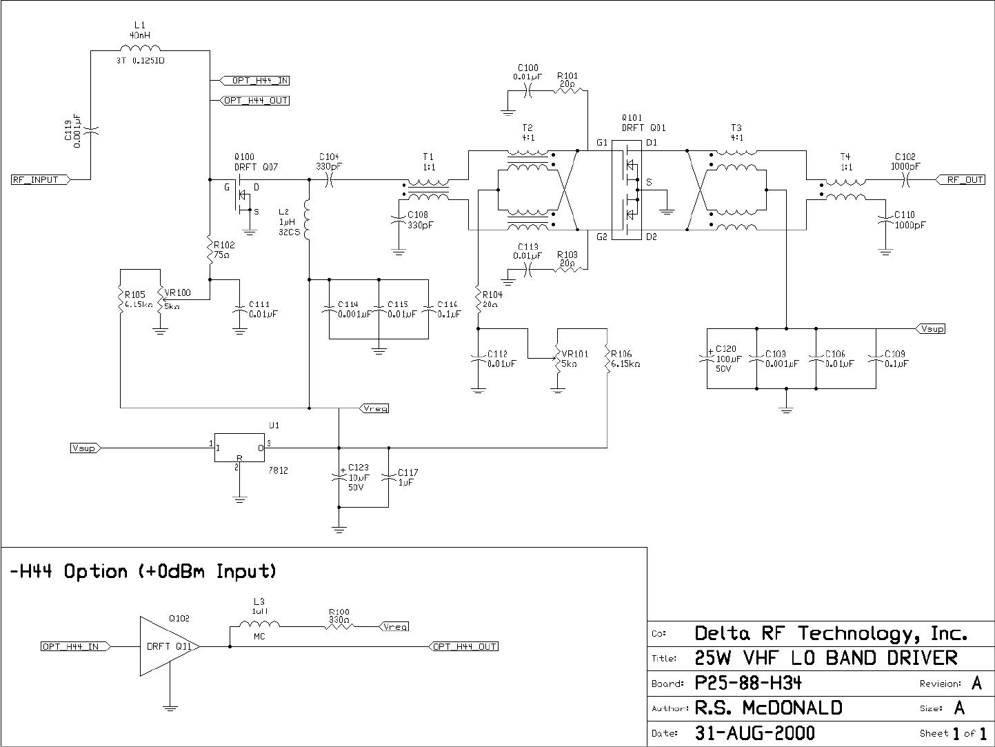
The PA25-VHF pallet is a two stage ultra linear class-A linear pallet. The PA25-VHF-L has a typical gain of
40dB and the PA25-VHF-H has a typical gain of 34dB. These pallets draw no more than 3.0Adc total drain
current (the exact bias and drain currents of your system are found in the spec sheet supplied with each
manual). The quiescent and drain currents can be measured on the PA25-VHF pallet by measuring the voltage
drop across the current sense resistor found directly at the DC power supply lead input to the pallet. This
resistance is 0.01-ohms, providing a 10mV per ampere ratio.
The final amplifier stages are comprised of (2) P400-VHF-L or P400-VHF-H amplifier pallets and are each
characterized with minimum gains of 18 dB (low band) or 15 dB (high band) and maximum drain currents of
28 A (low-band) or 20 A (high-band).
All currents on the driver and final stages can be measured across the on-board shunt resistor (0.01-ohm)
found at the DC supply inputs. With this resistance, a 1mV reading across this resistor indicates a current
draw of 1.0A.
A
A
1
1
TECHNALOGIX LTD.
25 W VHF LO BAND DRIVER
P25-VHF-L
R.S. MCDONALD
14 SEPTEMBER, 2000
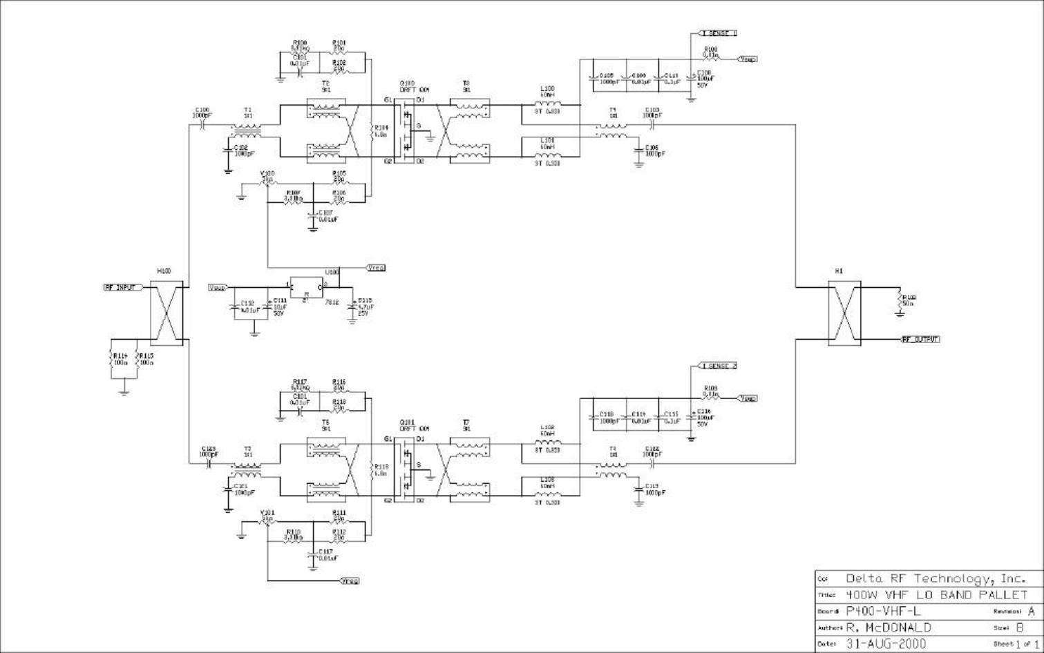
TECHNALOGIX LTD.
400W VHF LO-BAND PALLET
P400 VHF-L
R.S. MCDONALD
31 AUGUST, 2000
A
B
1
1

IV-4
Power Divider/Combiner (internal to each TAV-500 enclosure)
A Wilkinson power divider and combiner (identical printed circuit boards) are used to split the RF signal into, and
combine the amplified RF signal out of the (2) P400-VHF final amplifier pallets. Flanged power resistors help
ensure that any differences between the inputs or outputs is balanced.
The Wilkinson design takes advantage of the fact that an impedance transformation can take place across a
quarter-wavelength transmission line if the line has a different impedance than the source or load impedances
being matched. In this case, quarter-wavelengths of 75-ohm coaxial are used to maintain 50-ohm impedances at
the input and output of the Wilkinson divider/combiner. Due to its electrical and mechanical symmetry, the
Wilkinson design’s performance over moderate bandwidths is superior to other types. This design maintains
phase and amplitude equality, in addition to providing isolation and matched outputs.
Final Combiner (internal to combiner enclosure)
The RF outputs from the (2) TAV-500 amplifier modules then pass into a final enclosure where the signals are
combined, then filtered and monitored once again. The combiner is a 2-way, 1000-watt isolated power combiner
with a maximum phase imbalance of +/-1 degree. Minimum isolation is -18 dB and maximum insertion loss is -
0.45 dB from 170 to 280 MHz. Minimum return loss from ports 1 to 2 (input to input) is -25 dB and -20 dB on
port 3 (output).

IV-5
Directional Coupler (internal to TAV-500 and combiner enclosures)
The Technalogix dual directional couplers provide DC voltages proportional to forward and reflected RF power
monitoring. These analog voltages are converted for processing using a 10-bit analog-to-digital converter and
provide the control system with valuable data for monitoring purposes. The directional couplers installed in the
power amplifier and filter enclosures have peak detection circuits on the forward RF power side of the coupler
and average detection circuits on the reflected RF power side of the coupler. This is to allow the end user to
set power in a manner that is more independent of modulation and closer to a true tip-of-sync meter. Hence, the
readings on the displays in the power amplifier system are peak for forward and average for reflected. Output
power should be set by the following procedure:
THE POWER OUTPUT SHOULD NEVER BE ADJUSTED EXCEPT
UNDER THE TEST CONDITIONS OF NO AURAL CARRIER, WITH THE
VISUAL CARRIER MODULATED WITH SYNC AND BLANKING.
The directional coupler has a typical insertion loss of 0.05dB and its Type N connectors can handle 1,500 watts
peak. The coupler requires 8 to 8.5Vdc to power the internal electronics of the coupler and is supplied from the
control printed circuit board at the front of each enclosure.
Filter
The passive bandpass filter rejects spurious and harmonic output products and passes the VHF channel RF
output. The cavity resonator uses aperture coupling and is a linear resonator design. Typical insertion loss is 0.6
dB to 1.0 dB depending on channel frequency. Average roll off is –33 dBc at a point 4.5 MHz below the peak
visual carrier frequency and –30 dBc 9.0 MHz above the peak visual carrier frequency. The filter is DC grounded
on both the input and output for additional lightning protection.

V-1
Section V – Power Supply
Switching AC-DC power supplies are used to power the amplifier pallets, the control circuits, and all
of the fans. There are (2) power supplies paralleled in the power supply enclosure to generate the
necessary current for the amplifier pallets. These (2) supplies are paralleled at 31.0 Vdc nominally
and fed to the power amplifier enclosure via 4-AWG multi-stranded conductors and high current
connectors. There are no power supplies internal to the power amplifier enclosure, with the
exception of those found on the Series IIG control PCB. All fans run off this same supply, though
they pass through a series dropping resistor to lower the supply voltage, as the fans are 24Vdc.
A 24Vdc nominal power supply is located in the combiner enclosure. It simply supplies power to the
control PCB and the cooling fan.
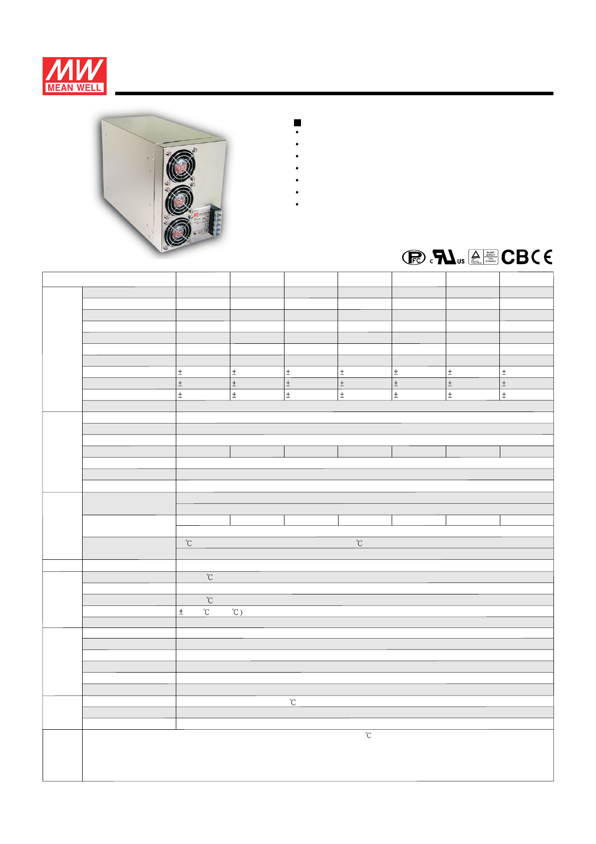
The power supplies in the power supply enclosure are Mean Well PSP-1500. The power supply
found in the filter enclosure is a Mean Well S60-24. The switching power supplies are fully protected
against short circuit and output overload. Short circuit protection is a cycling type power limit. The
internal AC fuse is designed to blow only on a catastrophic failure in the unit – the fuse does not
blow on overload or short circuit. The thermal shutdown automatically recovers when the power
supply chassis cools down.
AC (220Vac) is fed into the power supply enclosure via a terminal block and then through a
resettable circuit breaker. The AC for the combiner enclosure (110Vac) is fed through a filtered EMI
AC entry. The current in the power supply is then current limited with a resettable circuit breaker
before passing through a rocker switch. This switch turns the AC on and off to the switching power
supply.
OVERTEMPERATURE
Protectiontype:Shutdowno/pvoltage,re-powerontorecover
95 (TSW1)DetectontheheatsinkofPFCMOSFET 90 (TSW2)Detectthewindingofoutputchoke
SPECIFICATION
PSP-1500-5 PSP-1500-12 PSP-1500-13.5 PSP-1500-15 PSP-1500-24 PSP-1500-27 PSP-1500-48
MODEL
DCVOLTAGE
RATEDCURRENT
CURRENTRANGE
RATEDPOWER
OUTPUT VOLTAGE ADJ.RANGE
LINEREGULATION
LOADREGULATION
SETUP,RISE,HOLDTIME
VOLTAGERANGE
FREQUENCY RANGE
POWERFACTOR
EFFICIENCY (Typ.)
INPUT
INRUSHCURRENT(max.)
LEAKAGECURRENT
SAFETY STANDARDS
HARMONICCURRENT
EMSIMMUNITY
WORKINGTEMP.
WORKINGHUMIDITY
REMOTECONTROL
STORAGETEMP.,HUMIDITY
TEMP.COEFFICIENT
VIBRATION
MTBF
DIMENSIONOTHERS
NOTE
PACKING
OVERLOAD
OVERVOLTAGE
FUNCTION
ACCURRENT
5V 12V 13.5V 15V 24V 27V 48V
217.5A 112.5A 100.5A 90A 56.4A 50.4A 28.5A
0~217.5A 0~112.5A 0~100.5A 0~90A 0~56.4A 0~50.4A 0~28.5A
1087.5W 1350W 1356.75W 1350W 1353.6W 1360.8W 1368W
1200W 1500W 1500W 1500W 1500W 1500W 1500W
100mVp-p 150mVp-p 150mVp-p 150mVp-p 150mVp-p 150mVp-p 200mVp-p
4.75~5.5V 10~13.2V 12~15V 13.5~18V 20~26.4V 24~30V 41~56V
6.0% 3.0% 2.0% 2.0% 1.0% 1.0% 1.0%
0.5% 0.3% 0.3% 0.3% 0.2% 0.2%0.2%
2.0% 0.5% 0.5% 0.5% 0.5% 0.5%0.5%
1.5s,50ms,15ms/230VACatfullload
176~264VAC248~370VDC
47~63Hz
PF>0.95/230VACatfullload
77% 84% 84% 84% 85% 85% 86%
10.5A/230VAC
100A/230VAC
<3.5mA /240VAC
115~140% ratedoutputpower
5.75~6.75V 13.8~16.2V 15.5~18.2V 18~21V 27.6~32.4V 31~36.5V 57.6~67.2V
Protectiontype:Constantcurrentlimiting,recoversautomaticallyafterfaultconditionisremoved
UL1950, TUVEN60950 Approved
CompliancetoEN55022(CISPR22)ClassB
Complianceto EN61000-3-2,-3
Complianceto EN61000-4-2,3,4,5,6,8,11;ENV50204,EN55024,Lightindustrylevel,criteria A
-10~+65 (Refertooutputloadderatingcurve)
20~90%RHnon-condensing
-20~+85 ,10~95%RH
0.03%/ (0~50
10~500Hz,2G10min./1cycle,60min.eachalongX, Y,Zaxes
43.4Khrsmin.MIL-HDBK-217F(25 )
278*129*190.5mm(L*W*H)
6.9Kg;2pcs/13.8Kg/1.14CUFT
FileName:PSP-1500-SPEC2004-02-04
RC+/RC-:0~0.8V=poweron;4~10V=poweroffsinkcurrent<30mA
Protectiontype: Shutdowno/pvoltage,recoversautomaticallyaftertemperaturegoesdown
1500WSingleOutputwithPFCFunction
AC input active surge current limiting
Built-in active PFC function, PF>0.95
Protections:Short circuit/Over load/Over voltage/Over temperature
Built-in constant current limiting circuit
Built-in remote ON-OFF control
Built-in remote sense function
3 years warranty
Features :
PSP-1500 se r ie s
WITHSTANDVOLTAGE
ISOLATIONRESISTANCE
I/P-O/P:3KVACI/P-FG:1.5KVACO/P-FG:0.5KVAC
I/P-O/P,I/P-FG,O/P-FG:100MOhms/500VDC
ENVIRONMENT
SAFETY &
EMC
(Note5)
PROTECTION
EMICONDUCTION&RADIATION
PEAKLOAD Note.4
RIPPLE&NOISE(max.) Note.2
VOLTAGETOLERANCE Note.3
1. All parameters NOT specially mentioned are measured at 230VAC input, rated load and 25 of ambient temperature.
2. Ripple & noise are measured at 20MHz of bandwidth by using a 12" twisted pair-wire terminated with a 0.1uf & 47uf parallel capacitor.
3. Tolerance : includes set up tolerance, line regulation and load regulation.
4. 10% Duty cycle maximum within every 30 seconds(max.). Average output power should not exceed the rated power.
5. The power supply is considered a component which will be installed into a final equipment. The final equipment must be re-confirmed that it still meets
EMC directives.
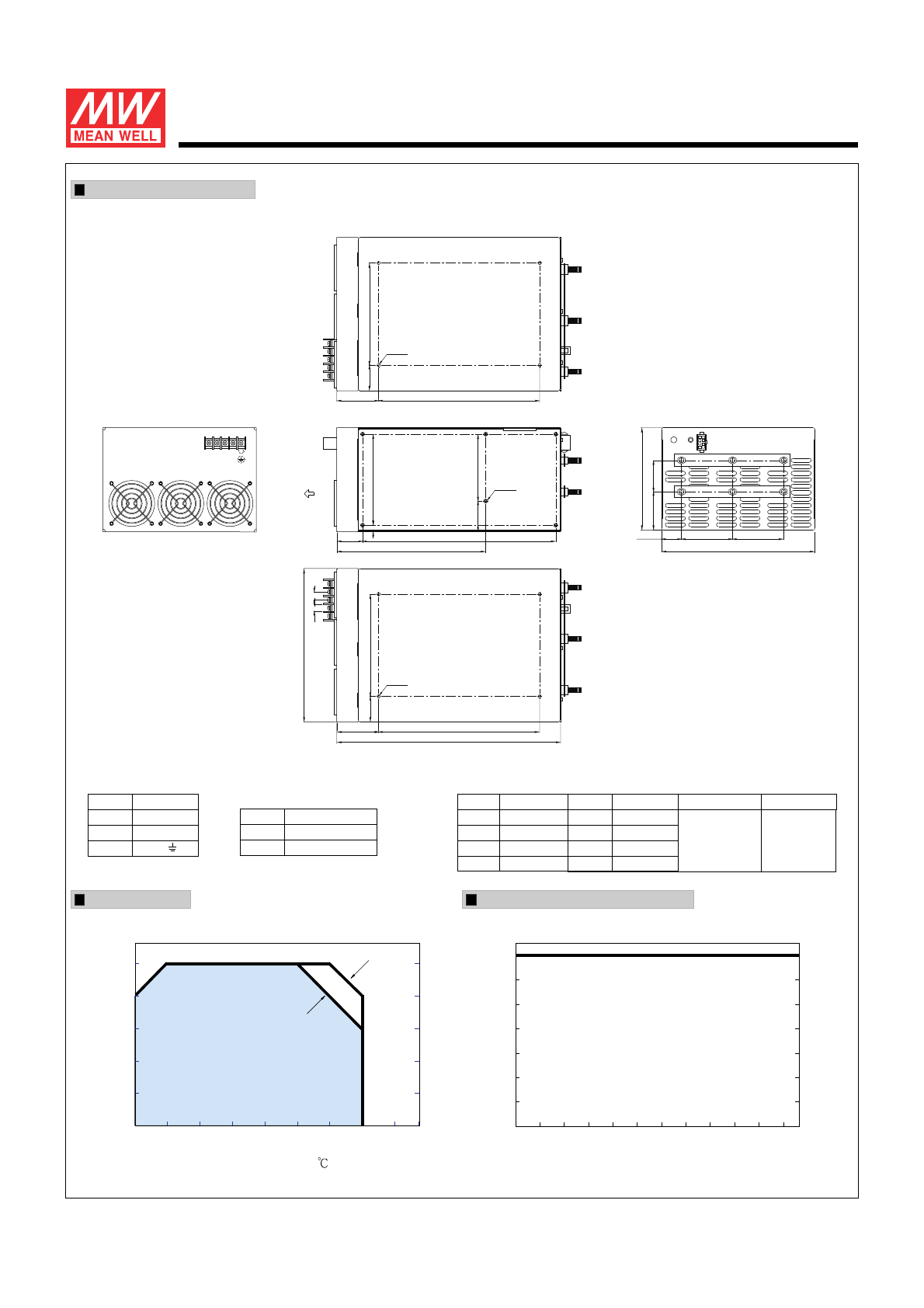
MechanicalSpecification
DeratingCurve
FileName:PSP-1500-SPEC2004-02-04
CaseNo.925Unit:mm
AMBIENTTEMPERATURE( ) INPUTVOLTAGE(V)60Hz
176 264
100
90
80
70
60
50
40
LOAD(%)
LOAD(%)
-10 0 10 20 30 40 50 60 70
20
40
60
80
100
12~48V
5V
ControlPin.No Assignment:MOLEX5559-NP uses5558malecrimpterminal
PinNo.PinNo.
51
62
7
8
3
4
AssignmentAssignment
NCNC
NC-S
+S
RC+
G
RC-
Matingconnector
MOLEX5557-NR
Terminal
MOLEX5556
Femalecrimp
Terminal
receptacle
ACInput TerminalPin.No Assignment
PinNo.
1
3
2
Assignment
FG
AC/N
AC/L
DCOutput TerminalPin.No Assignment
PinNo.
1,3,5
2,4,6
Assignment
DCOUTPUT +V
DCOUTPUT -V
LED
ADJ 26
15
48
37
1
O/P
2
4-M4
I/P
10
7
2
1
3
Airflow
direction
52 200
278
31.75 127
190.5
6-M3
32 240
185
24.75 63.5 63.5
190.5
47.5 39
12
9
CONTROL
4-M4
52 200
31.75 127
8 113
38 83
3
4
5
6
OutputDeratingVSInputVoltage
1500WSingleOutputwithPFCFunction P S P - 1 5 0 0 s e ri e s
MEAN WELL
SWITCHING POWER SUPPLY
ISO-9001 CERTIFIED MANUFACTURER
S-60
SERIES
.LOW COST, HIGH RELIABILITY .COMPACT SIZE, LIGHT WEIGHT
.105ºC OUTPUT CAPACITOR .100% FULL LOAD BURN-IN TEST
.INTERNATIONAL AC INPUT RANGE .BUILT IN EMI FILTER, LOW RIPPLE NOISE
.HIGH EFFICIENCY, LOW WORKING TEMPERATURE
.SOFT-START CIRCUIT, LIMITING AC SURGE CURRENT
.SHORT CIRCUIT, OVERLOAD, OVER VOLTAGE PROTECTED
MODEL
SPECIFICATION S-60-5S-60-12 S-60-15 S-60-24
DC OUTPUT VOLTAGE 5V 12V 15V 24V
OUTPUT V. TOLERANCE ±2% ±1% ±1% ±1%
OUTPUT RATED CURRENT 12A 5A 4A 2.5A
OUTPUT CURRENT RANGE 0-12A 0-5A 0-4A 0-2.5A
RIPPLE & NOISE 120mVp-p120mVp-p150mVp-p150mVp-p
LINE REGULATION ±0.5% ±0.5% ±0.5% ±0.5%
LOAD REGULATION ±1% ±0.5% ±0.5% ±0.5%
DC OUTPUT POWER 60W 60W 60W 60W
EFFICIENCY 73% 76% 77% 79%
DC VOLTAGE ADJ. +10,-5% ±10% ±10% ±10%
INPUT VOLTAGE RANGE 85~264VAC 47~63Hz; 120~370VDC
AC CURRENT 2A/115V 1A/230V
INRUSH CURRENT COLD START 30A/115V 60A/230V
LEAKAGE CURRENT <3.5mA/240VAC
OVERLOAD PROTECTION 105%~150% TYPE:PULSING HICCUP SHUTDOWN RESET:AUTO RECOVERY
OVER VOLTAGE PROTECTION 115%~135%
OVER TEMP. PROTECTION ----------
TEMP. COEFFICIENT ±0.03% / ºC (0~50ºC)
SETUP, RISE, HOLD UP TIME 800ms, 50ms, 10ms / 115VAC 300ms, 50ms, 80ms / 230VAC
VIBRATION 10~500Hz, 2G 10min./1cycle, PERIOD FOR 60min. EACH AXES
WITHSTAND VOLTAGE I/P-O/P:3KVAC I/P-FG:1.5KVAC O/P-FG:0.5KVAC
ISOLATION RESISTANCE I/P-O/P, I/P-FG, O/P-FG:500VDC / 100M Ohms
WORKING TEMP., HUMIDITY -10ºC~+60ºC(REFER TO OUTPUT DERATING CURVE), 20%~90% RH
STORAGE TEMP., HUMIDITY -20ºC~+85ºC, 10%~95% RH
DIMENSION 159*97*38mm CASE:901
WEIGHT 0.55Kgs
SAFETY STANDARDS UL1012, TUV EN60950, IEC950, UL1950 APPROVED
EMC STANDARDS CISPR22 (EN55022), IEC801-2,3,4, IEC555-2 VERIFICATION
NOTE : 1.ALL PARAMETERS ARE SPECIFIED AT 230VAC INPUT, RATED LOAD, 25ºC 70% RH. AMBIENT.
2.TOLERANCE GINCLUDE SET UP TOLERANCE, LINE REGULATION, LOAD REGULATION.
3.RIPPLE & NOISE ARE MEASURED AT 20MHz BY USING A 12" TWISTED PAIR TERMINATED WITH A 0.1uF & 47uF CAPACITOR.
4.LINE REGULATION IS MEASURED FROM LOW LINE TO HIGH LINE AT RATED LOAD.
5.LOAD REGULATION IS MEASURED FROM 0% TO 100% RATED LOAD.
6.C2,3,6 MUST BE REMOVED. 2000-10-03

VI-1
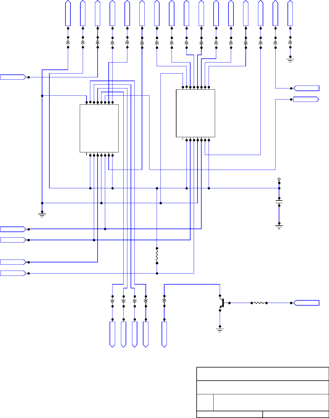
Section VI – Monitor and Control System
Control Board Overview (Series II-rev I)
The control printed circuit boards (PCB) are located at the front of each enclosure connected directly
to the back of the liquid crystal displays (LCD) and are identified as Series II – rev I PCBs. The main
purpose of the Series II - rev I PCB is to monitor the RF power and the DC supply voltages in the power
amplifier and filter enclosures and to monitor just the DC supply voltages in the power supply
enclosure. In all cases, a DC voltage proportional to the parameter being sampled is conditioned,
protected, buffered, and then run into an analog-to-digital converter (ADC) where software processes
the signal. The software processing determines if the parameters are within the predetermined safe
operating levels and displays the parameters on the LCD for monitoring purposes. The Series II - rev I
PCB can be broken apart into (5) main component areas: the power supply, interface, signal
processing, display, and microcontroller. Schematics are found later in this section.
Power Supply Components
There are (4) power supply voltages generated on the Series II – rev I PCB:
1. +5Vdc for all logic and general purpose PCB supply voltage.
2. +4Vdc for the LED backlighting on the LCD
3. -4Vdc for the contrast voltage required by the LCD
4. +5Vdc for the directional coupler supply
The +5Vdc is generated from a small switching power supply comprised of C101, C102, D102, L101,
and U101. This power supply accepts DC input voltages up to 40Vdc (unless U101 is an HV option,
then the maximum input voltage is 60Vdc) and outputs +5Vdc at up to 1Adc. This voltage is always on,
as the ON/OFF pin on U101 is hard-wired to the on configuration. C103, L102, and C104 form a noise
choke to help filter and switching noise or RF noise that may radiate onto the control circuit board.
The +4Vdc is generated from a small switching power supply comprised of components C105, C106,
D103, L103, and U102. This power supply accepts DC input voltages up to 40Vdc (unless U102 is an
HV option, then the maximum input voltage is 60Vdc) and outputs +5Vdc at up to 1Adc. The voltage
then gets dropped down to +4Vdc through R101. This backlight voltage can be turned on and off via
the ON/OFF pin on U102. The PCB is setup in a manner that allows this voltage to be hard-wired on all
the time or controlled from the microcontroller through latch U111. This selection is made with jumper
J102.
The -4Vdc is generated using a switched capacitor voltage converter design, using components C109,
C110, R102, R103, U104, and VR101. U4 accepts +5Vdc from the general purpose +5Vdc supply and
generates -5Vdc. This voltage then gets dropped across the voltage divider (R102, R103) to generate
the contrast voltage specific to the LCD that is installed in the system.
The voltage required by the directional coupler is generated with a standard linear voltage regulator,
U103. C107 and C108 helps clean up any ripple or noise that might be on the output voltage. In the
standard configuration, where the directional coupler requires 5Vdc, the 5Vdc is simply taken from the
U101 filtered power supply output.

VI-2
Interface Components
The interface section of the Series II – rev I PCB includes the front panel switch interfacing in
addition to the buzzer and carrier disable output circuits.
The (4) membrane switches found on the front panels of each enclosure are tied to the
microcontroller through an isolation stage to avoid any static discharge or noise on the switch
wiring from reaching the microcontroller. Optoisolators U105 and U106, in addition to components
R104…R115 create the necessary isolation to the sensitive microcontroller. By depressing any
membrane switch, a ground (0V) is applied to the input of the optoisolators. The optoisolators will,
in turn, output a ground (0V) to the microcontroller.
The membrane switches found on the front panels of the enclosures operate in the following
manner with a depress:
POWER – When unit is plugged in, AC is supplied to the fan and switching power supply input,
but the amplifiers are still turned off. In order to turn the amplifiers on, wait ten seconds after
plugging the PA in and push in the “POWER” tactile button. The LCD will read “Soft Start Warm
Up, Please Wait”. After ten seconds the bias voltages will be turned on and you may then plug in
the RF drive. Depress for (1) second to turn on and (3) seconds to turn system off. In the case of
multiple enclosures, all POWER switches are tied together in each enclosure, so only one needs
to be depressed.
NAVIGATE – Turns on backlight to LCD and displays forward and reflected RF power and DC
supply voltage parameters. When power amplifier is first turned on, the LCD comes on
automatically and this information is displayed. Information is displayed for approximately 2
minutes before the backlight turns off and the display is cleared. This is set up so as not to burn
any pixels into the LCD from extended on time. In the case of multiple enclosures, the NAVIGATE
switches are individual to each enclosure.
SELECT – Turns on backlight to LCD and displays forward and reflected RF power and DC
supply voltage parameters. When power amplifier is first turned on, the LCD comes on
automatically and this information is displayed. Information is displayed for several minutes
before the backlight turns off and the display is cleared. This is set up so as not to burn any
pixels into the LCD from extended on time. In the case of multiple enclosures, the SELECT
switches are individual to each enclosure.

VI-3
RESET – Tactile switch resets the monitor and control system. The amplifier gets shut down for
under 0.5 seconds and comes back on with each depress of the reset button. At the same time,
all fault counters in the microcontroller software are reset and the LCD is reset in the same
manner as it is with a depress of the NAVIGATE button. Reset switches are individual to each
enclosure but may be tied together externally through the remote port, as explained later in this
section.
The buzzer control comes from pin 7 on microcontroller U114. The control signal turns on the base
of transistor Q101, which allows current to flow through the single tone magnetic buzzer. Jumper
J105 simply turns off the buzzer.
The carrier disable circuit simply applies a shutdown voltage to the driver pallet in the system. The
U114 generates the signal out of pin 21 and controls transistor Q102 through R117. When Q102 is
turned off, the shutdown voltage to the driver is floating and the carrier is on. During a fault
condition, when Q102 is turned on, the shutdown voltage is applied to the carrier disable on the
driver. Relay K101, which outputs the carrier disable, is protected from transient spikes by D104.
Signal Conditioning Components
The signal processing section of the Series II – rev I PCBs is used to buffer potentially noisy or
damaging signals from the ADC. Power supply samples and forward and reflected power from a
directional coupler are then digitized.
Firstly, all analog signals are protected with a resettable fuse and transient voltage suppressor
(TVS) combination. These components ensure that voltages above the Vbr breakdown voltage of
the TVS get clamped and do not pass farther down the circuit. After this protection stage, the
analog voltages get dropped with voltage dividers to safe levels for the buffers and ADC. For
example, a 30Vdc power supply sample gets dropped to a level below the +2.5Vdc voltage
reference of the ADC. After the voltage dividers, the analog signals get buffered with U107 and
U108, configured as unity gain voltage followers. Finally, after some further decoupling capacitors
and filters, the analog signals get digitized by the 8-channel, 10-bit ADC (U10) and sent to the
microcontroller through a serial interface.
In the power amplifier and filter enclosures, there are (3) analog voltages that get conditioned and
processed: DC power supply sample, forward RF power, and reflected RF power. Specifically, the
components for the power amplifier and filter enclosure conditioning are as follows:
DC power supply – J108 (pin 1 floating and direct connection), F107, C120, L108,
C121, R129, R130, VR105, U8, C122, C123, L109, C124 and
U10.
Forward RF power – J108 (pin 2), F106, D109, C117, C118, L107, C119, R127, VR104,
R128, U108, C108, C125, L110, C126, C127, and U110.
Reflected RF power – J108 (pin 3), F105, D108, C114, C115, L106, C116, R125, VR103,
R126, U108, C130, L112, C131, C132, and U110.

VI-4
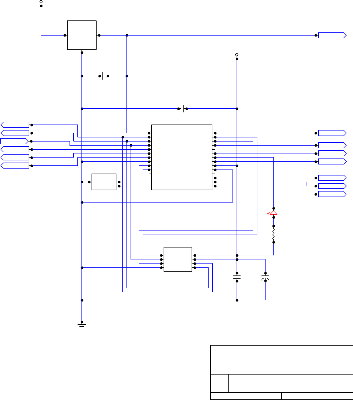
Display Components
The display section of the Series II – rev I PCB is comprised of the LCD and the components that
make up the data bus to send the data from the microcontroller to the LCD.
Specifically, the LCD is an alphanumeric 20X4 display that uses the industry standard 44780
controller and a parallel interface for data communications. Firstly, the microcontroller sends out
the data to be displayed via a serial bus where the signals are latched with U111 and U112 and
converted to a parallel data stream. The parallel data then transfers directly to the LCD through
connector J109. J109 also carriers the power supply for the LCD.
Microcontroller Components
The heart of the monitor and control system found in Series II - rev I PCBs is microcontroller U114.
This microcontroller analyzes all RF power levels and voltages to ensure that all operating
parameters are within their predetermined safe operating levels. If a fault is found, appropriate
action is taken to help protect the system from damage, which may include turning the RF carriers
off. A full description of all faults and their respective actions is found later in this section.
The power supply for the microcontroller is monitored closely via supervisor U113. Should the
+5Vdc supply drop below +4.5Vdc, a microcontroller reset is generated to ensure there are no
brown out conditions that may latch the microcontroller up to an unknown state. The front panel
Reset momentary switch is also tied to this line after optoisolation. The microcontroller is run off of
a 4.000MHz clock source, generated by ceramic resonator CR101. If the software is running, LED
D110 will be lit. Finally, U115 stores all characters for the LCD to minimize the overhead required
for the microcontroller, and also stores the current state of the power ON/OFF of the system. This
is to ensure that, in the event of a power outage, the system returns to the exact state is was
before power was interrupted.
VI-5
Fault Shutdowns
On the LCD (Liquid Crystal Display) the following messages may appear:
If you see this message, the system will:
- shut amp down for 1 minute
- automatically turn amp on after 1 minute and check again for overdriven amplifier
- come back to the same power level that it was set
If you see this message, the system will:
- shut amp down for 5 minutes
- automatically turn amp on after 5 minutes and check again for high VSWR
- come back to the same power level that it was set

VI-6
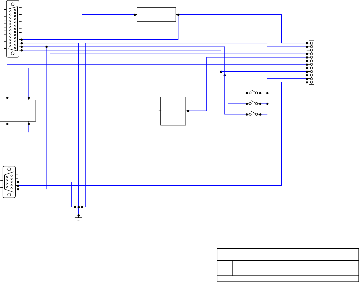
Remote Port
The remote port allows external control of the transmission system via the DB25 connector on each
enclosure. All functions on the remote port are simply hard-wired or paralleled to existing wiring to
provide a secondary method of control to the user, and are activated as follows:
pin 1: ground to reset microcontroller, float otherwise
pin 2: ground for 2 seconds to toggle carrier on/off, float otherwise
pin 3: common ground
pin 4: DC power supply sample
Series II - Bill of Materials
I
21-Jun-05
Item Qty Components Description Tolerance Package Equivalency
1 1
BZ101
BUZZER, magnetic, 5V, single tone SMD CT-1205C
CUI CT-1205C
2 2 C101, C105 CAPACITOR, electrolytic, 100uF, 63V <=20% SMT (Panasonic VS "G" size) Panasonic ECE-V1JA101P, NIC NACEW101M63V10x10.5
3 2 C102, C106 CAPACITOR, electrolytic, 330uF, 35V <=20% SMT (Panasonic VS "G" size) Panasonic ECE-V1VA331P, NIC NACEW331M35V10x10.5
4 21
C103, C104, C107,
C112, C113, C115,
C116, C118, C119,
C120, C121, C123,
C124, C125, C126,
C128, C129, C130,
C131, C133, C134 CAPACITOR, ceramic, 0.01uF, 63V <=20% SMT 0805 Digikey C0805C103K5RACTU
5 7
C108, C111, C140,
C143, C144, C145,
C146 CAPACITOR, ceramic, 0.1uF, 25V <=20% SMT 1206 Utech GMC31X7R104K50NT
6 2
C109, C110
CAPACITOR, electrolytic, 100uF, 25V <=20% SMT (Panasonic VS "E" size) Panasonic ECE-V1EA101UP
7 7
C114, C117, C122,
C127, C132, C135,
C147 CAPACITOR, tantalum, 1uF, 16V <=20% SMT 3216 Sprague 293D105X9035B2T
8 1 CR101
CLOCK, ceramic resonator, 4.000 MHz,
w/caps
f <= 0.5%
C <= 20% Through hole, 3-position, 0.1" spacing ECS Inc. ZTT-4.00MG
9 1 D101
TV Power Amplifier: DIODE, TVS, 600
watts, Vwm=30V, Vbr min=33.3 SMB Crydom SMBJ30A; GI SMBJ30A
10 1 D101
FM Power Amplifier: DIODE, TVS, 600
watts, Vwm=48V, Vbr min=53.3 SMB Crydom SMBJ48A; GI SMBJ48A
11 2
D102,D103
DIODE, schottky, If=3A, Vr=60V SMC International Rectifier 30BQ060
12 1
D104
DIODE, rectifier, If=1A, Vr=200V SMA
Diodes Inc S1D-13
13 2 D108, D109
DIODE, TVS, 600 watts, Vwm=5.0V, Vbr
min=6.4 SMB Crydom SMBJ5.0A; GI SMBJ5.0A
14 1
D110
DIODE, LED, RED, clear or diffused SMT 1206 Lumex SML-LX1206IW
15 1 F101
FUSE, resettable, Ihold=0.75A, Itrip=1.5A,
Vmax=72V 0.23" lead spacing, 20AWG leads Raychem RXE075; Bourns MF-R075
16 3 F105, F106, F107
FUSE, resettable, Ihold=0.14A,
Itrip=0.34A, Vmax=60V miniSMD Raychem miniSMDC014-2
17 1 J101
CONNECTOR, 4-position plug, 180
degree wire entry, 90 degree screw
access, 5.08mm 0.2" spacing Wieland 25.340.3453, Weco 10.808.104
18 1 J101
CONNECTOR, 4-position header,
pluggable, vertical, closed, 5.08mm Through hole, 0.2" spacing Wieland 25.350.3453, Weco 20.806.128
19 2 J102, J106
CONNECTOR, breakaway header strip, 3-
position, 0.1", square post Through hole, 0.1" spacing Molex 22-28-4300; Samtec TSW-130-05-T-S
20 1 J105
CONNECTOR, breakaway header strip, 2-
position, 0.1", square post Through hole, 0.1" spacing Molex 22-28-4300; Samtec TSW-130-05-T-S
21 3
J102, J105, J106
CONNECTOR, 2-position post shunts
0.1" spacing
AMP 382811-6; Samtec SNT-100-BK-T
22 1 J103
CONNECTOR, 5-position plug, 180
degree wire entry, 90 degree screw
access, 5.08mm 0.2" spacing Wieland 25.340.3553.0
23 1 J103
CONNECTOR, 5-position header, 0.1",
vertical Through hole 0.2" spacing Wieland 25.350.3553.0
24 2 J107, J108
CONNECTOR, 3-position plug, 180
degree wire entry, 90 degree screw
access, 5.08mm 0.2" spacing Wieland 25.340.3353, Weco 10.808.103
25 2 J107, J108
CONNECTOR, 3-position header,
pluggable, vertical, closed, 5.08mm Through hole, 0.2" spacing Wieland 25.350.3353, Weco 20.806.127
26 1
J109
CONNECTOR, terminal strip, 16-position Through hole, 0.1" spacing Samtec TSW-116-18-T-S
27 1
J109
CONNECTOR, socket strip, 16-position Through hole, 0.1" spacing Samtec SSW-116-03-T-S
28 1
K101
RELAY, DPDT, 5V, 2Adc contact, SMD Relay - Aromat - TX SA Aromat TX2SA-5V
29 1 L101
INDUCTOR, 680uH, Irms=0.4A,
DCR=2.02 ohms SMT JW Miller 3316-681M
30 10
L102, L105, L106,
L107, L108, L109,
L110, L111, L112, L113
INDUCTOR, 0.01uH, Imax=0.45A,
DCR=0.13 omhs +/- 10% SMT 1210 KOA KL32TE010K
31 1 L103
INDUCTOR, 680uH, Irms=1.3A, DCR=0.2
ohms SMT (Talema S5) Talema SWS-0.85-680
32 1 LCD101
20 X 4 character liquid crystal display,
LED backlit 4-40 pem mount (4) Varitronix 20464K
33 1 PCB101
Series II, revision H printed circuit board,
soldermask, silkscreen, FR4 Alberta Printed Circuits, MPC, GRM, Enigma, …
34 2 Q101, Q102 TRANSISTOR, NPN, Ic=1A, Vce=40V SMT SOT-23
Fairchild MMBT2222A; Zetex FMMT2222A; Diodes Inc
MMBT2222A-7
35 1 R101 RESISTOR, 4.7 ohm, 1/2 watt, carbon film 5% SMT 2010 Panasonic ERJ-12ZYJ4R7U
36 1 R102
RESISTOR, 15.0 ohm, 1/10 watt, thick
film 1% SMD 0805 Panasonic ERJ-6ENF15R0V
37 1 R103
RESISTOR, 75.0 ohm, 1/10 watt, thick
film 1% SMD 0805 Digikey MCR10EZHF1001, Panasonic ERJ-6ENF75R0V
38 11
R104, R105, R106,
R109, R110, R111,
R112, R115, R116,
R132, R134
RESISTOR, 1.00 kohm, 1/10 watt, thick
film 1% SMD 0805 Panasonic ERJ-6ENF1001V
39 4
R107, R108, R113,
R114
RESISTOR, 10.0 kohm, 1/10 watt, thick
film 1% SMD 0805 Panasonic ERJ-6ENF1002V
revision:
date:
Optional part depending on power level of TV or FM
Series II - Bill of Materials
I
13-Apr-05
40 1 R117
RESISTOR, 4.99 kohm, 1/10 watt, thick
film 1% SMD 0805 Panasonic ERJ-6ENF4991V
41 1
R124
RESISTOR, 13 kohm, 1/8 watt
1% SMD 0805 Rohm MCR10EZHF1302
42 4
R125, R127, R126,
R128 RESISTOR, 1 kohm, 1/8 watt 1% SMD 0805 Rohm MCR10EZHF1001
43 1
R129
RESISTOR, 121 kohm, 1/8 watt
1% SMD 0805 Rohm MCR10EZHF1213
44 1
R130
RES, 2.15 kohm, 1/10 watt, thick film 1% SMD 0805 Rohm MCR10EZHF2151
45 1
R131
RES, 120 ohm, 1/10 watt, thick film 1% SMD 0805 Panasonic ERJ-6ENF1200V
46 2 U101, U102
TV Power Amplifier: REGULATOR,
switching, 5Vdc, 3A, fosc=52kHz SMD TO-263-5 National LM2576S-5.0
47 2 U101, U102
FM Power Amplifier: REGULATOR,
switching, 5Vdc, 3A, fosc=52kHz SMD TO-263-5 National LM2576HVS-5.0
48 1 U104 REGULATOR, inverter, 100mA SMD SOIC-8
National LM2660M; Analog Devices ADM8660, Maxxim
MAX660
49 2
U105, U106
OPTOISOLATOR, dual, Viso=5300Vac
SMD DIP8 Fairchild MCT6S
50 1
U108
OP AMP, quad, low voltage
SMD SOIC-14 National LMV324M
51 1 U109
REFERENCE, 2.50V (for TV PA >=
250Wpk) +/-0.2% SMD SOT-23 National LM4040BIM3-2.5
52 1
U110
ADC, 10-bit, 10-channel
SMD SOIC-20 Analog Devices AD7812YR
53 2 U111, U112 LOGIC, 8-bit shift register with latches SMD SOIC-16
Fairchild MM74HC595M; On Semi MC74HC595AD; Phillips
74HC595D
54 1 U113
SUPERVISOR, n-channel, open drain,
internal pullup resistor SMD SOT-23 MCP130T-450I
55 1 U114
MICROCONTROLLER, OTP, 4k, 22 I/O
lines Through hole DIP-28 Microchip PIC16C63A-04/SP
56 1 J111
Connector, socket, 28-position, DIP, 0.3"
spacing Through hole DIP-28 Jameco 112299CL or equivalent
57 1
U115
MEMORY, 8k X 8, EEPROM, SPI
SMD SOIC-8
Microchip 25LC640I/SN
58 1
VR101
do not stuff
59 4
VR102, VR103, VR104,
VR105 RES, variable, 10 kohm, 1-turn, 3mm SMD Bourns TC33 Bourns TC33X-2-103E
date:
revision: Optional part depending on power level of TV or FM
BK LT
CTRL
SELECT
1
SERIES II, REV. I - Control System
+5Vdc
C107
Vin Cond
C104C103
L102
VR101
+
C109
+
C110
P1
P2
P3
P4P5
P6
P7
P8
U104
BkLtCtrl
GND
Vcoupler
GND
Vin L101
D102
+
C101
D101
F101
3
J101 1Vin
2
Vout
4
Feedbk
3Gnd
5On/Off
U101
+
C102
+5Vdc
4
J101
+
C105
+
C106
2Vin
1
Vout
4
Feedbk
3Gnd
5On/Off
U102
D103
L103
Pin15LCD
IN
COM
OUT
U103
C108
1
J101
J101
2
+5Vdc
Pin3LCD
J102
R103
R102
R101
A. Sivacoe
SERIES II: Control System
I Power Supply Section
Date: March 28, 2005 Page: 1 of 1
Rev ID
Buzzer
delete
2
SERIES II, REV. I - Control System
D104
J104 3
J104 5
SEL In J104 4
J104 2
NAV In
J104 1
+5Vdc
J106
J103 5
Ground
J103 3
J103 4
J103 2
+5Vdc
+5Vdc
R104
R117
J107
2
Q102Rly.Ctrl
+5Vdc
K101
Rly. COM
Rly. N/O
Rly. N/C
J107
3
J107
1
Buzzer
J105
Q101
+5Vdc
R116
RES In
NC(RC6)
VW In
PWR In J103 1
P1
P2
P3
P4 P5
P6
P7
P8
U106
P1
P2
P3
P4 P5
P6
P7
P8
U105
R105 R106
R109 +5Vdc
R107 R108
VW uPC
PWR uPC
R115
R110 R111 R112
+5Vdc
R113 R114
PIN17uPC
RES uPC
BZ101
A. Sivacoe
SERIES II: Control System
I Interface Section
Date: March 21, 2005 Page: 1 of 1
Rev ID
3
For U7
PSU
FWD
RFL
Low Threshold Adjust
SERIES II, REV. I - Control System
J108
4
Analog 4
VR105
VR104
VR103
C121
L108
C120
Vin Cond
+
C117
+
C114
C119C118
L107
L106
C116C115
VR102
5
6
411
7
+
U108
2/4
3
2
411
1
+
U108
1/4
10
9
411
8
+
U108
3/4
12
13
411
14
+
U108
4/4
J108
1
Analog 1
J108 2
Analog 2
J108 3
Analog 3
Isoltd 4
Isoltd 3
Isoltd 2
Isoltd 1
C112
F107
F106
F105
D108
D109
C113
+5V
L105
D107
D106
F103
F104
C111
Isoltd 6
Isoltd 7
Isoltd 8
12
13
411
14
+
U107
4/4
J108
8
Analog 8
D105
F102
Analog 7 J108
7
Analog 6 J108
6
Analog 5 J108
5
9
10
411
8
+
U107
3/4
3
2
411
1
+
U107
1/4
R124
R130
R129
R128
R127
R126
R125
R119
R118
R120
R121
R122
R123
A. Sivacoe
Series II: Control System
I Analog Input Section
Date: March 21, 2005 Page: 1 of 1
Rev ID
Pin 3 on U109 is left
unconnected on PCB
4
FWD
PSU
RFL
Low Thresh
SERIES II, REV. I - Control System
C133
L113
C130
L112
C125
L110
C123
L109
C129C128
L111
2 1
U109
+5Vdc
For U110
C140
+
C142C141
+
C139C138
+
C137C136
+
C135C134
+
C132C131
+
C127C126
C124
+
C122
DtoUPC
DfromUPC
Dclk
ConvStrt
Isoltd 1
Isoltd 2
Isoltd 3
Isoltd 4
Isoltd 6
Isoltd 7
Isoltd 8
Vref
Cref
Vin1
AGND
Vin2
Vin3
Vin4
Vin5
Vin6
Vin7 Vin8
A0
DGND
TFS
RFS
Dout
Din
Dclk
ConvStart
Vdd
U110
R131
A. Sivacoe
Series II: Control System
I Analog Conversion Section
Date: March 21, 2005 Page: 1 of 1
Rev ID
SERIES II, REV. I - Control System
5
U11: LCD control signals,
LCD backlight control, and
External interface outputs
U12: LCD data bus (D0...D7)
D0...D7 is text or instruction
Pin3LCD
uPCPIN14Q103
1
Ext. PSU
serial_out
reset
shift_clk
latch_clk
output_en
serial_in
Qa(out_1)
Vcc Qb(out_2)
Qc(out_3)
Qd(out_4)
Qe(out_5)
Qf(out_6)
Qg(out_7)
Qh(out_7)
GND
U112
Latch2CS
Latch1CS
+5Vdc
C143
BkLtCtrl
Pin15LCD
234
Unbuf A
Unbuf B
Unbuf C
Unbuf D
1615
LED A
LED K
32
J109
1
LCD Vo
LCD Vdd
LCD Vss
654 78910111213
LCD RS
LCD R/*W
LCD E
LCD D6
LCD D5
LCD D4
LCD D3
LCD D2
LCD D1
LCD D0
LCD D7
Dclk
DfromUPC
14
J110
5
serial_out
reset
shift_clk
latch_clk
output_en
serial_in
Qa(out_1)
Vcc Qb(out_2)
Qc(out_3)
Qd(out_4)
Qe(out_5)
Qf(out_6)
Qg(out_7)
Qh(out_7)
GND
U111
R133
R132
A. Sivacoe
Series II: Control System
I LCD Section
Date: March 2, 2005 Page: 1 of 1
Rev ID
SERIES II, REV. I - Control System
6
+
C147
C144
D110
Dclk
DtoUPC
Dig.In 3
Dig.In 2
Dig.In 1
C146
Buzzer
Latch2CS
Latch1CS
DfromUPC
Rly.Ctrl
Reset
Dig.Out2
CONVST
Dig.Out1
Vcc
C145
+5Vdc
MCLR/Vpp
RA0
RA1
RA2
RA3
RA4
RA5
Vss
OSC1/CLKin
OSC2/CLKout
RC0/T1CKI
RC1/CCP2
RC2/CCP1
RC3/SCK/CL RC4/SDI/SDA
RC5/SD0
RC6/TX/CK
RC7/RX/CK
Vss
Vdd
RB0/INT
RB1
RB2
RB3
RB4
RB5
RB6
RB7
U114
*CS
SO
*WP
Vss SI
SCK
*HOLD
Vcc
U115
Vcc
GND
Reset
U113
OSC1
OSC2
GND
CR101
R134
A. Sivacoe
Series II: Control System
I Microcontroller Section
Date: March 2, 2005 Page: 1 of 1
Rev ID
On/Off Input
View Input
Reset
Pallet Disable
RFL in
FWD in
+8Vdc
Ground
Vin
-
green
blue
red 22AWG
red 18AWG
purple
brown
green
green
green
purple
orange
yellow
red 22AWG
grey
green
brown
1
3
4
3
2
2
1
1
STAR POINT GND
-+
J1 2
J1 1
J1 3
J1 4
J6 2
J3 2
J7 7
J7 6
J3 3
J3 1
J3 5
J3 4
Control PCB
Series IIG
ON/OFF
VIEW
RESET
PSU
GND
OnOff
RESET
DB25
Remote Port
GND
FAULT
ONOFF
CTRL
DB9
RFL
FWD
8V
GND
Coupler
Directional
V V
DC Supply
DB9
Pallet
Driver
Series II Control System Wiring
G
Date: December 17, 2003 Page: 1 of 2
Rev ID

VII-
1
Section VII – Mechanical Section
The heat sink allows the amplifiers to operate at a cooler temperature and prevents overheating, which helps
the longevity of the entire system. The heat sink has hollow fins, which help dissipate the heat from the
amplifiers faster than a conventional serrated or corrugated fin.
In addition to the cooling effects of the heat sink, within each 500-watt power amplifier enclosure, there are
four fans that each provide 170 cubic feet per minute (CFM) of air flow (into zero static pressure). There are
two fans mounted at the front of the heat sink and two mounted at the back end of the heat sink operated in
a push-pull configuration to assist with heat dissipation. The fans are a 24Vdc variety, so there are series
dropping resistors to drop the higher power supply voltage down to a safe level.

Technalogix Ltd.
VIII-1
Section VIII - Installation
This section contains unpacking, inspection, and installation instructions for the power amplifier. We
are sure that you are chomping at the bit to install your new system, so we recommend that you read
the following sections very carefully.
Building Recommendations
The quality of the building is of great importance if you are to expect long life and continued
performance from the power amplifier. The building must be clean, dry, temperature controlled and
secure. Don’t forget to allow space in the building for any additional racks to house test equipment, a
workbench area, line regulating transformers, ladders, equipment and parts storage, first aid kit,
emergency generator if used, as well as heating and cooling devices that may be unique to your
installation. A sloping roof will tend to develop leaks less rapidly. The building should be well roofed
with good material. The cooling load will be lowered with reflective or light colored roofing material.

Technalogix Ltd.
VIII-2
Heating and Cooling Requirements
The environment’s temperature will contribute greatly to the length of the power amplifier’s life.
Technalogix recommends that the building’s filtered air intake must have capacity for all air-flow in the
building plus an additional 20%. The TAV-1000 uses (10) ball bearing fans – (4) for each power
amplifier, (1) for the power supply enclosure, and (1) for the combiner. Keep the intake below the
roofline to avoid intake of solar heated air. Please ensure that the intake and exhaust areas are on the
same side of the building to avoid pressure differentials during windy conditions. Also, do not position
intake near exhaust’s preheated air. If air conditioning is required to cool the shelter, discuss the
situation with a qualified HVAC technician. Under average conditions, 12,000 BTUs will cool
approximately 500 square feet to a comfortable level.

Technalogix Ltd.
VIII-3
Electrical Service Recommendations
Technalogix recommends that a qualified, licensed local electrician be consulted for the required
electrical service. We suggest local electricians because:
• The personnel knows the local codes
• The personnel can be on site readily
• You are apt to get better overall support if you give what business you can to local suppliers
Technalogix recommends that proper AC line conditioning and surge suppression be provided on the
primary AC input to the power amplifier. All electrical service should be installed with your national
electrical code in your area, any applicable provincial or state codes, and good engineering practice.
Special consideration should be given to lightning protection of all systems in view of the vulnerability
of most transmitter or translator sites to lightning. Lightning arrestors are recommended in the service
entrance. Straight and short grounds are recommended. The electrical serviced must be well
grounded. Do not connect the unit to an open delta primary power supply, as voltage fluctuations could
harm the unit. Branch your circuits. Do not allow your lights, your workbench plugs, and your
transmitting or translating equipment to operate on one circuit breaker. Each transmitter or translator
should have its own circuit breaker, so a failure in one does not shut off the whole installation.

Technalogix Ltd.
VIII-4
Antenna and Tower Recommendations
Your preliminary engineering workgroup should establish your antenna and tower requirements, both
for receiving and transmitting antennas. Construction of sturdy, high quality antenna/tower systems will
pay off in terms of coverage of your service area, the overall quality and saleability of your radiated
signal, and reduced maintenance expenses. Technalogix provides complete turnkey antenna systems
if needed. If your site is serving as a translator, your receiving antenna should be in line of sight to the
originating station all year round. The foliage will change with season. Transmitting antennas can
enhance or seriously impair the transmitter/translator output.
The selection, routing, and length of coaxial cable are extremely important in the installation. If there is
a 3 dB line loss in the cable between your unit’s output and the transmitting antenna, a 1000-watt unit
will only deliver 500 watts to the antenna. Buy the best cable you can obtain, route it via the shortest
way to the antenna, and keep it straight. Do not form it into sharp bends on its way. Do not use any
more cable fittings for the installation than absolutely necessary. All cautions here apply equally to all
coaxial cables in the system - input and output.
Pay attention to radial ice accumulation when designing the transmission system. It is not uncommon
for at least an inch of ice to build up on the tower and antenna. This in turn significantly increases the
weight, cross section, and wind loading of the system.
Attaching the transmission line to the tower is crucial to maintain a safe and reliable operation. Nylon
wire ties and electrical tape will breakdown in the sunlight and ultimately fail, creating a potentially
dangerous situation. It is important to use proper clamps and hoisting grips and also ensure that the
transmission line is grounded to the tower in several locations. When high currents flow through the
tower in the event of lightening strikes, some of that current will flow through the outer conductors of
the transmission lines. Due to the resistance difference between the steel tower and copper
transmission line, a significant voltage can be developed, often resulting in arcing between the outer
jacket and outer conductor, thus pitting the conductor.
• Preventative maintenance is crucial in ensuring that safety is maintained. Specifically, check that
transmission line grounds are tight and are not missing any hardware. Frequently inspect
support clamps or spring hangers. Consider investing in an ice break (ice bridge), if you
haven’t already done so, as shards of falling ice can damage the transmission line – and if it is
going to happen, it will happen at an important time. Check the tower light photocells and
conduit.
The better-known tower manufacturers offer complete technical and safety documentation with their
towers. Be sure that you have this information as it regards wind loading, guying, etc. The best-
designed antenna system will function poorly if shortcuts and compromises are used during installation.
Follow the manufacturer’s instructions exactly, along with any engineering data prepared for the site.
Be absolutely safe and certain about this aspect as human lives may be at stake.

Technalogix Ltd.
VIII-5
Shelter Security
The FCC requires that the transmitter or translator be secure from entry or control by unauthorized
persons, and that any hazardous voltages or other dangers (including most tower bases) be protected
by locks or fences as necessary to protect personnel and prevent unauthorized tampering or
operation. Security of the building further implies that it be secure from wildlife. Use sturdy construction
materials, including sheet metal if necessary. Holes around conduit, cable, and other similar entry
points should be stuffed with steel wool and caulked to prevent entry of wildlife. Other features of
security for your shelter may include its location with respect to the prevailing wind conditions. A
location leeward of some natural topographical feature will prevent wind damage and snowdrifts. Check
the soil runoff conditions that may slow or hasten wind or water erosion and other concerns that may
be unique to your location.

Technalogix Ltd.
VIII-6
Unpacking and Inspection
Check the outside of the container. Carefully open the container and remove the power amplifier.
Retain all packing material that can be reassembled in the event that the equipment must be returned
to the factory.
Exercise care in handling equipment during inspection to prevent damage due
to rough or careless handling.
• Visually inspect the enclosure of the power amplifier for damage that may have occurred during
shipment.
• Check for evidence of water damage, bent or warped chassis, loose screws or nuts, or
extraneous packing material in connectors or fan failures.
• Inspect all connectors for bent connector pins.
• If the equipment is damaged, a claim should be filed with the carrier once the extent of the
damage is assessed. Technalogix cannot stress too strongly the importance of immediate
careful inspection of the equipment and subsequent immediate filing of the necessary claims
against the carrier if necessary.
• If possible, inspect the equipment in the presence of the delivery person. If the equipment is
damaged, the carrier is your first area of recourse.
• If the equipment is damaged and must be returned to the factory, phone for a return
authorization.
• Claims for loss or damage may not be withheld from any payment to Technalogix, nor may any
payment due be withheld pending the outcome thereof. Technalogix cannot guarantee the
carrier’s performance.
Technalogix Ltd.
VIII-7
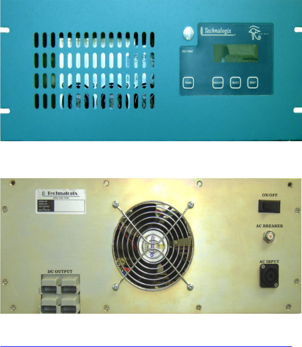
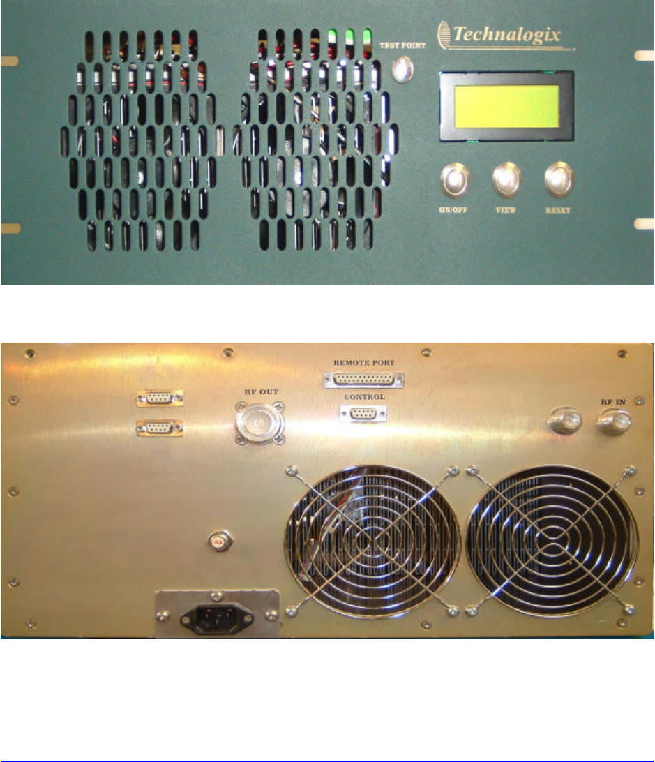
Location and Function of Controls and Connectors (Power Supply)
The following illustration depicts the location of the connectors when installing the power supply.

Technalogix Ltd.
VIII-8
POWER - Tactile button to turn carriers on and off. To turn off, must be depressed for
at least 2 seconds. Tied internally through DB9 connectors to all other
POWER buttons.
NAVIGATE - Tactile button to refresh screen after two minute screen saver times out. All
monitoring and protection continues during screen saver.
SELECT- Tactile button to refresh screen after two minute screen saver times out. All
monitoring and protection continues during screen saver.
RESET - Tactile button to reset microcontroller in control board. Also clears existing
faults. Individual control board with reset comes back on with soft start feature.
AC IN – AC input to switching power supply. Switching power supply draws a maximum
of 30 AAC at 220 VAC.
AC BREAKER – 30-ampere resettable circuit breaker is used to protect against inrush
currents and high current draw from switching power supply. The thermal
circuit breaker is a single pole configuration.
PA PSU - DC supply outputs to each power amplifier. DC cabling is identical and can
be hooked up to PA2.
AC ON/OFF - AC rocker swith (SPST) to supply AC to the AC-DC switching power supply.
Technalogix Ltd.
VIII-9
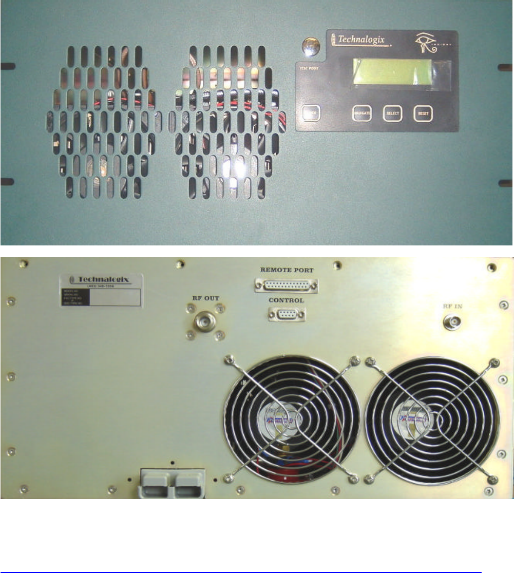
Location and Function of Controls and Connectors (TAV-500 Power Amplifier)
The following illustration depicts the location of the connectors when installing each of the 500-watt
power amplifiers (TAV-500).

Technalogix Ltd.
VIII-10
POWER - Tactile button to turn carriers on and off. To turn off, must be depressed for
at least 2 seconds. Tied internally through DB9 connectors to all other
POWER buttons.
NAVIGATE - Tactile button to refresh screen after two minute screen saver times out. All
monitoring and protection continues during screen saver.
SELECT- Tactile button to refresh screen after two minute screen saver times out. All
monitoring and protection continues during screen saver.
RESET - Tactile button to reset microcontroller in control board. Also clears existing
faults. Individual control board with reset comes back on with soft start feature.
RF IN – RF input from the output of the RF splitter. BNC connector, 50 Ω.
RF OUT – 500-watt RF output to be combined with the other 500-watt output. Connects to
RF IN PA 1 or 2 on combiner unit. N connector, 50 Ω.
PA CTRL – Control signals communicating with the combiner enclosure. Connects with the
PA 1 and PA 2 CTRL connector on the combiner. DB9 connector (see Amplifier
Monitoring section for pinout description).
DC IN – DC input from switching power supplies.
REMOTE PORT - pin 1: ground to reset microcontroller, float otherwise
pin 2: ground for 2 seconds to toggle carrier on/off, float otherwise
pin 3: common ground
pin 4: DC power supply sample
Technalogix Ltd.
VIII-11
Location and Function of Controls and Connectors (Combiner / Filter Enclosure)
The following illustration depicts the location of the connectors when installing each of the 500-watt
power amplifiers (TAV-500).

Technalogix Ltd.
VIII-12
ON/OFF - Momentary pushbutton to turn carriers on and off. To turn off, must be depressed for at
least 2 seconds. Tied internally through DB9 connectors to all other ON/OFF buttons.
VIEW - Momentary pushbutton to refresh screen after two minute screen saver times
out. All monitoring and protection continues during screen saver.
RESET - Momentary pushbutton to reset microcontroller in control board. Also clears existing
faults. Individual control board with reset comes back on with soft start feature.
PA1 and PA2 RF IN – RF input from the output of each power amplifier. N connector, 50 Ω.
RF OUT – 1,000-watt RF output to be connected with inline wattmeter and then to antenna. N
connector, 50 Ω.
PA CTRL – Control signals communicating from the combiner enclosure to the power amplifier
enclosures. Connects with the PA 1 and PA 2 CTRL connector on the combiner. DB9
connector (see Amplifier Monitoring section for pinout description).
REMOTE PORT - pin 1: ground to reset microcontroller, float otherwise
pin 2: ground for 2 seconds to toggle carrier on/off, float otherwise
pin 3: common ground
pin 4: DC power supply sample
AC IN – AC input to switching power supply. Switching power supply draws a maximum of 2
AAC at 110 VAC.

Technalogix Ltd.
VIII-13
Initial Hook Up
1. Ensure that the antenna has been swept and has a return loss of greater than 20dB (VSWR =
1.2:1). This should be done before connecting the antenna cable to the transmitter output.
2. Check that your video source is
3. Place the transmitter/translator in its permanent location near a receptacle supplying required
AC voltage.
DO NOT APPLY AC POWER AND TURN ON POWER TO THE TRANSMITTER /
TRANSLATOR AT THIS TIME SINCE THE RF OUTPUT MUST BE PROPERLY
LOADED BEFORE OPERATION.
4. Place an appropriate AC power line protector, conditioner, and/or surge suppressor across the
AC supply line.
5. Hook up the modulator or processor as shown in their respective manuals for a transmitter or
translator. Do not connect the modulated signal from the RF OUT on the modulator or
processor to RF IN on the power amplifier at this time. Because of the characteristics of
LDMOS devices, the RF drive should not be connected to the power amplifier until after the
power supply and bias voltages are present and stable.
6. Ensure that modulator or processor RF output level is turned down as far as possible.
7. Ensure that the audio modulation is set to 100% with the audio signal supplied, as described in
the appropriate modulator/processor manual (will be factory set).
8. Ensure that the video modulation level is set to 87.5% with the video signal supplied, as
described in the appropriate modulator/processor manual (will be factory set).
9. Install the DB9 cables from each power amplifier enclosure to the combiner/filter enclosure.
It does not matter which DB9 cable is used as they are both identical.
10. Install the DC power supply leads (4 AWG) between the power supply enclosure and each
power amplifier enclosure. Ensure that each connector is securely locked into it’s mating
connector.
11. Hook up the RF cabling from the output of each power amplifier to the RF input on the
combiner/filter enclosure.
12. Connect the transmitting antenna cable to the RF OUT N-type connector on the filter enclosure
RF output.

IX-1
Section IX - Operating Procedure
Assuming the previous installation instructions have been completed and cautions noted, and the TAV-
1000 power amplifier is ready to receive a properly modulated video and audio signal, proceed with the
following steps to place the system in operation. The TAV-1000 power amplifier has been factory
aligned for channel frequency (per system specification), signal levels and optimum performance.
IT IS HIGHLY RECOMMENDED THAT YOU RUN YOUR SYSTEM INTO A DUMMY LOAD BEFORE
INSTALLING TO MAKE SURE THERE ARE NO DAMAGES CAUSED IN SHIPPING AND THE UNIT IS
RUNNING PROPERLY
1. Do not apply RF drive signal to the power amplifier at this time.
2. Verify that all control and RF cables are tight and properly seated in or on the mating connector.
3. Plug the modulator or processor into AC mains (110Vac).
4. Plug the 4U combiner/filter enclosure into AC mains (110Vac).
5. Switch AC rocker switch to “ON” position.
6. Verify that the combiner enclosure’s fan is on.
7. Plug the 4U power supply enclosure into 220V AC mains.
8. Verify that the power amplifier fans are all on.
9. Ensure that the modulator/processor is turned on and set up according to its instructions. Depress
the POWER tactile button to turn the unit on.
10. The internal soft start circuitry will turn the bias voltages off until the power supply to the amplifier
pallets is fully stable. The message on the LCD indicates when the soft start is running. Once
complete, the Forward and Reflected Power and Power Supply readings will appear on the LCD in
the filter and power amplifier enclosures.
11. After the soft start is complete, apply the RF drive signal (which still should be turned down)
between the modulator or processor and the power amplifier RF In. This ensures that the RF drive
signal is applied only after the power supply is stable and the bias voltages are applied to the
amplifier.

IX-2
12. The TAV-1000 LCDs show the user the present status of the amplifiers. Adjust RF output power to
desired level (see Important RF Power Notice in previous section). Verify that the FWD Power
reads 800 to 1,000 Watts on the combiner/filter enclosure - depending on signal content. The
system is set up for 1,000 watts peak visual power using the sync and blanking signal and should
read 1,000 watts FWD Power on the LCD under this condition only. The output power level can
be adjusted using the modulator or processor’s RF output level adjust. Keep in mind that the
system will shut down should the forward RF output power level be exceeded.
13. Ideally, the RFL Power should read zero. However, should a high VSWR be detected, the system
will automatically shut down and cycle as previously described. This is also a peak wattage
reading.
14. Verify that the power supply reads approximately 30 Volts DC (see supplied final inspection sheet
for factory settings of power supply levels) on the LCD of the power amplifier and power supply
enclosures and 24Vdc on the combiner/filter enclosure.
15. Look at the transmitted output using a suitable monitor. The picture and sound quality should be
clean and sharp. If the output picture and sound quality is unsatisfactory, check the input signals,
connections to the antenna system, antenna and transmission line VSWR, and the physical
condition of the antenna.
If reception problems are encountered, and the quality of transmission is satisfactory, the difficulty is
often with the receiving antenna or with obstructions in the path between the transmitter/translator and
receiver.

X-1
Section X – Maintenance and Troubleshooting
Periodic Maintenance
If your unit employs a filter on the air inlet for the fans, the filter should be cleaned every 30 days. If the
equipment is operated in a severe dust environment, the filters on the inlet fan may need to be cleaned more
regularly. Turn the system off and unplug all of the AC inlet cords. The filter can be lifted off the fan and
cleaned using an air compressor at low pressure. While the filter is out, clean the fan blades themselves with a
small brush. The fans themselves do not need lubrication.
The interior of the cabinets should be cleaned and inspected annually. Turn the system off and unplug all of
the AC inlet cords. Remove the top lid by unscrewing the 6-32 machine screws.
Use extreme caution when working near the AC input terminal. The power amplifier and
power supply store hazardous capacitances and voltages.
Using either compressed air or a brush with soft bristles, loosen accumulated dust and dirt and then vacuum the
interior of the cabinet. Complete a visual inspection of the interior, making sure there are no loose connections
or discolorations on any components from heat. Nothing inside the power amplifier enclosure exceeds a
temperature that is not comfortable to the touch under normal operating conditions, so any signs of discoloration
indicate potential damage.
All modular components inside the enclosure are attached to aluminium mounting plates for easy removal and
replacement. Ensure that plates are secured and the mounting hardware is tight.

X-2
Troubleshooting
The first and most important aspect of troubleshooting anything is to be systematic. Note where you have
looked and what you found.
Look first for the obvious.
• Make a physical inspection of the entire facility. Are all necessary connections properly made? Do you
see any signs of obvious damage within the equipment?
• Is the AC power ‘ON’ to the site and the equipment? (Check fuses and circuit breakers if necessary.)
• Are all the switches in the correct operating position?
• Is the input signal present?
• Check LCD readings for presence of forward and reflected power and 31 V DC supply levels.
The above is an aid in determining the fault if some aspect of the system is not operating. The following table
deals with quality of operation:
Symptom Possible Fault Correction
Horizontal bars in picture (may roll
either way depending on phase) AC grounding / AC interference Install EMI/RFI filter in AC line
Ensure modulator/processor and
power amplifier share a common
ground
Diagonal lines in picture Interference Install EMI/RFI filter in AC line
Determine source and frequency
of interfering signal (spectrum
analyzer may be required)

X-3
Symptom Possible Fault Correction
Weak output or picture Low level input signal Verify presence and level of input
signal
Low output power Verify power amplifier output with
wattmeter and dummy load
Incorrect modulation depth Adjust to meet specification
High reflected power Incorrect load Ensure amplifier connected to
transmission line
Ensure correct antenna impedance
(50 ohms)
Check antenna tuning and
VSWR. Verify correct cable for
transmission line length
Check all cables for visible
damage (kinks, nicks or cuts)
Check all connectors for poor
connections, water or corrosion
Check alignment of antenna
Check for physical damage of
antenna, including ice build-up
Thank you
for choosing
Technalogix Ltd.