Technalogix TM200 LICENSED BROADCAST STATION MODULATOR User Manual TM 200 rev 1 02 Feb 2007
Technalogix, Ltd. LICENSED BROADCAST STATION MODULATOR TM 200 rev 1 02 Feb 2007
USERS MANUAL

TM-200 Broadcast Modulator
OPERATING MANUAL

TM-200 Issue 1.02 November 2005 Page 1 of 64
TABLE OF CONTENTS
1.0
S
AFEGUARDS
................................................................................................................................... 2
General Safeguards ........................................................................................................................... 2
Safety and First Aid............................................................................................................................ 3
2.0
W
ARRANTY
...................................................................................................................................... 4
3.0
D
ESCRIPTION AND
S
PECIFICATIONS
................................................................................................... 5
General Description ........................................................................................................................... 5
Standard Features.............................................................................................................................. 5
Available Options ............................................................................................................................... 6
Block Diagram .................................................................................................................................... 7
Specifications ..................................................................................................................................... 9
Signal Conditioning Module............................................................................................................ 11
4.0
I
NSTALLATION
................................................................................................................................ 12
Building Recommendations............................................................................................................ 12
Heating and Cooling Requirements ............................................................................................... 12
Electrical Service Recommendations ............................................................................................ 13
Antenna and Tower Recommendations......................................................................................... 14
Shelter Security ................................................................................................................................ 15
Unpacking and Inspection .............................................................................................................. 16
Location and Function of Controls and Connectors.................................................................... 17
5.0
O
PERATING
P
ROCEDURE
................................................................................................................ 19
Preliminary Hook-up ........................................................................................................................ 19
Setup of Output Level and Channel Selection .............................................................................. 20
Setup of Video Input Connection and Adjustment ....................................................................... 21
Setup of Baseband Audio Input Connection and Adjustment .................................................... 22
Setup of 4.5 MHz Sub-Carrier Audio Input Connection and Adjustment ................................... 23
Setup of IF Pre-Correction on Signal Conditioning PCB ............................................................. 24
Setup of Sync Level on Signal Conditioning PCB........................................................................ 25
Automatic Shut Down ...................................................................................................................... 26
Transmitter Hookup ......................................................................................................................... 27
6.0
P
ROBLEM
T
ROUBLESHOOTING
G
UIDE
............................................................................................. 28
7.0
B
ILL OF
M
ATERIALS
,
S
CHEMATICS
,
AND
PCB
O
VERLAYS
................................................................ 29
Agile Logic Board Bill of Materials................................................................................................. 29
Agile Output Amplifier Bill of Materials ......................................................................................... 34
Audio Video Modulator Board Bill of Materials............................................................................. 37
Signal Conditioning Bill of Materials.............................................................................................. 46
Digital Up converter Bill of Materials ............................................................................................. 50
750 MHz Down Converter Bill of Materials .................................................................................... 56
Power Supply Bill of Materials........................................................................................................ 61

TM-200 Issue 1.02 November 2005 Page 2 of 64
1.0
S
AFEGUARDS
General Safeguards
This section is written as a general guide for those having previous knowledge and
experience with these kinds of equipment. It is not intended to contain a complete
statement of all safety precautions, which should be observed by personnel using this or
other electronic equipment.
To reduce the risk of fire or electric shock, do not expose this equipment to rain or
moisture. Do not open the cabinet. Refer servicing to qualified personnel.
1. READ INSTRUCTIONS - All safety, installation, and operating instructions should be
read before the equipment is operated.
2. RETAIN INSTRUCTIONS - The safety and operating instructions should be retained
for future reference.
3. FOLLOW INSTRUCTIONS - All safety, installation, and operating instructions should
be followed.
4. GROUNDING AND POLARIZATION - The TM-200 Modulator is equipped with a
three prong grounded power plug. Do not remove the ground prong from the plug.
Do not use an AC receptacle where the plug blades cannot be fully inserted.
5. SERVICING - Do not attempt to service this equipment yourself as opening or
removing covers may expose you to dangerous voltage or other hazards and will
void the warranty. Refer all servicing to qualified service personnel.
6. DAMAGE REQUIRING SERVICE - Unplug this equipment and refer servicing to
qualified service personnel under the following conditions:
• if the power cord or plug is damaged.
• if liquid has been spilled or objects have fallen into the equipment.
• if the equipment has been exposed to rain or water.
• if the equipment does not operate normally by following the operating
instructions. Adjust only those controls covered by the operating instructions. An
improper adjustment may result in damage and will often require extensive work
by a qualified technician to restore the equipment to its normal operation.
• if the equipment has been dropped or the cabinet has been damaged.
• if the equipment exhibits a distinct change in performance.

TM-200 Issue 1.02 November 2005 Page 3 of 64
Safety and First Aid
Personnel engaged in the installation, operation, maintenance, or servicing of electronic
equipment are exposed to the hazard of high voltage. It is imperative that all safety
regulations and precautions are consistently observed. Knowledge of first aid
procedures is recommended. The following information is presented as a reference
only.
• At all times, avoid placing any part of the body in series between ground and circuit
points, whether power is on or off.
• Dangerous voltage may be present in equipment even though power is off. Do not
open the cabinet. Refer servicing to qualified service personnel.
• It is the duty of all personnel to be prepared to give adequate emergency first aid
treatment and thereby prevent avoidable loss of life.
• There are three principle degrees of burns, recognizable as follows:
• a first-degree burn reddens the skin.
• a second-degree burn blisters the skin.
• a third degree burn chars the flesh and frequently places the victim in a state of
shock accompanied by respiratory paralysis.
• Respiratory paralysis can cause death by suffocation within seconds. It is imperative
that the approved methods of artificial respiration are initiated immediately and
continue until the victim’s breathing is normal.
• A muscular spasm of unconsciousness may render the victim unable to break free of
the electric power. If this is the case, turn the power off immediately.
DO NOT TOUCH THE VICTIM OR YOU MAY SHARE THE SAME
PREDICAMENT.
• If the power cannot be turned off immediately, very carefully loop a dry rope, article
of clothing, length of strong cloth or a rolled-up newspaper around the victim and pull
the victim free of the power source. Carefully avoid touching the victim or clothing.
• Once free of the power source, the victim must be placed in a reclining position and
covered with a blanket or newspapers to keep warm. At the first opportunity, enlist
help in summoning a doctor. If a doctor cannot be summoned, transport the victim to
the doctor or a hospital. Be sure the victim is kept well covered and warm while
awaiting professional treatment.

TM-200 Issue 1.02 November 2005 Page 4 of 64
2.0
W
ARRANTY
Technalogix Ltd. products have been completely tested and found to meet specifications
and be in proper operating condition. They are warranted to be free from defects in
materials and workmanship for a period of one year from the date of shipment.
Technalogix Ltd. will not be liable for damages of whatever nature arising out of or in
connection with the equipment or its use thereof. Technalogix does not assume
responsibility for injury or damage resulting from the practices of untrained or unqualified
personnel in the handling of this equipment.
Technalogix Ltd. warranty does not include:
• misuse, neglect or accident.
• incorrect wiring and /or improper installation.
• unauthorized repairs, modifications or use in violation of instructions issued by
Technalogix.
• incidental or consequential damages as a result of any defect.
• reshipment cost or insurance of the unit or replacement units or parts.
• acts of God.
Technalogix agrees, at our option, to remedy warranted defects or furnish a new part in
exchange for any part of a unit which, under normal installation, use and service,
becomes defective. The user will pay for transportation costs to and from the repair
center.
To claim your rights under this warranty:
• Contact Technalogix and describe the problem in as much detail as possible. See
troubleshooting section in this manual. If a solution cannot be found at this time, it
may be determined that the unit will have to be returned to Technalogix for repair.
• Package equipment carefully for prepaid shipment to Technalogix. Include a written
description of the problem experienced and a copy of the original invoice establishing
warranty status.
Technalogix reserves the right to make revisions in current production of the equipment
and assumes no obligation to incorporate these changes in earlier models.

TM-200 Issue 1.02 November 2005 Page 5 of 64
3.0
D
ESCRIPTION AND
S
PECIFICATIONS
General Description
The TM-200 is a high output modulator that eliminates the need for preamplifiers prior to
the power amplifier system. The modulator first processes baseband audio and video
information to provide an IF output consisting of a visual IF carrier at 45.75 MHz, using
amplitude modulation, and an aural IF carrier at 41.25 MHz, using frequency modulation.
Pre-correction is implemented at IF frequencies with a Signal Conditioning Board.
Frequency conversion circuitry then translates the modulator’s IF carriers to VHF and
UHF television frequencies. All operating controls are located on the front panel, and
will be discussed in later section, while input and output interfaces are on the back plate.
An aural loop through is provided to properly set transmitter power.
Standard Features
• Totally microprocessor controlled with self-diagnostic monitoring.
• Selectable output channels:
Standard Broadcast VHF 2 – 13, UHF 14 – 60, T7 – T13
HRC channels 1 through 118
±10 kHz offsets
• SAW filtered IF designed for adjacent channel operation.
• + 10 dBm (minimum) output using low distortion hybrid amplifiers.
• Synthesized oscillators – crystal referenced phase locked.
• Bar graph modulation and digital LED readout.
• Internal switch selects standard or HRC output.
• Surface mount technology construction.
• RF muted during tuning.
• Optional aural sub-carrier and baseband audio input
• Phase lock loop FM audio.
• BTSC stereo compatible.
• External separate audio/video and composite IF loop-through.
• RS-232 control option
• Sound carrier level adjustable –10 dB to –15 dB.
• Video delay pre-distortion network meets FCC 73.687.
• High stability TCXO, ± 250 Hz
• Non-volatile memory retains channel selection after power loss.
• Video Detection turns off carrier in event of loss of video.
• IF pre-correction allow slope/knee linearization of signal.
• Sync level adjustment to ensure sync tip at proper levels.
• White clip and DC restoration of baseband video signal.
• 50-ohm RF Output and tap-off
TM-200 Issue 1.02 November 2005 Page 6 of 64
Available Options
• 4.5 MHz sub carrier and baseband audio inputs.
• Dual RS-232 control with daisy chain capabilities that allow for remote control by
PC workstation.
• HRC Output Frequency Set - This feature is controlled by an internal dip switch
assembly, DS-1. The switch is located near the right front corner (with the panel
facing you) between the test point and the output converter module. DS-1 is
clearly marked on the PCB. Switch #3 placed in the OFF position switches the
output frequency to HRC on all channels. The switch is normally set to ON at the
factory.
TM-200 Issue 1.02 November 2005 Page 7 of 64
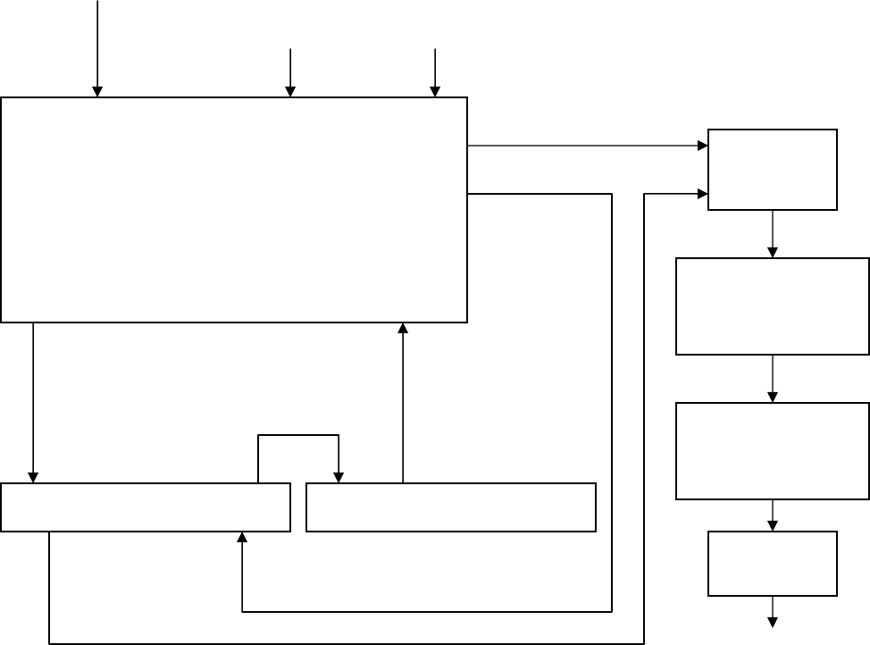
Block Diagram
The baseband input source enters through a Video In connector, and Baseband Audio In
or 4.5 Audio In connector on the back of the modulator. The connectors are mounted
directly on the A/V Modulation PCB where the IF output is generated. The baseband
video signal passes into the modulator, through a group delay filter, and onto the Signal
Conditioning PCB to the video detect/sync level adjust section. The IF signal from the IF
loop on the modulator is connected through the IF pre-correction portion of the same
Signal Conditioning PCB. The visual IF carrier and the aural IF carrier are then
combined before entering the Upconverter PCB. The outputs are at RF frequencies of
945.75 MHz for the visual carrier and 941.25 MHz for the aural carrier. Then, the signal
passes through a Downconverter section allowing a user selectable VHF or UHF
broadcast television channel. Finally, the signal passes through an output amplifier
which increases the RF signal level typically to 15 dBm.
TM-200 Issue 1.02 November 2005 Page 8 of 64
VIDEO IN AUDIO IN
Baseband Audio 4.5 MHz Audio
Aural IF Carrier
Visual IF Carrier
Video Detect
In Out
IF Pre-correction
Out In
RF Output
A/V Modulation PCB
Signal Conditioning Board Display and Control Board
Combiner
Upconverter
Downconverter
Output
Amplifier

TM-200 Issue 1.02 November 2005 Page 9 of 64
Specifications
RF Characteristics
Frequency range 7 to 750 MHz
Frequency Response (one channel) ±0.5 dB
Frequency Stability ±250 Hz
RF Output Level +60 dBmV max
Output Impedance 50 Ohms
Harmonics > 60 dB below rated power
Predominant Intermodulation Distortion dBc = decibels below visual carrier
+ 920 kHz
> -53 dBc
- 920 kHz
> -53 dBc
+ 2.66 MHz
> -53 dBc
- 2.66 MHz
> -53 dBc
+ 5.42 MHz
> -53 dBc
+ 7.16 MHz
> -53 dBc
3
rd
Order Intermodulation Distortion
+ 4.5 MHz
> -60 dBc
+ 9.0 MHz
> -60 dBc
All others
> -60 dBc
Spurious Emissions > -60 dBc
NTSC Video Characteristics
Input Level to modulator (for 87.5% modulation) 1.0 V
PP
Differential Phase (at 87.5% modulation) ±2 Degrees
Differential Gain (at 87.5% modulation) 2%
Group Delay < ±40 nS
Video Group Delay Pre-emphasis Conforms to IC/FCC specifications
K-Factor 1.9% for 2T Pulse
Hum and Noise > 60 dB below rated power
Aural Characteristics
Input: 50 Hz – 15 KHz 0 dBm (0.8V)
Impedance 600 ohms, balanced
Frequency Response +/- 1.0 dB
Frequency Tolerance, +/- 500 Hz 4.5 MHz
Frequency Deviation +/- 25 KHz
Harmonic Distortion 1% max
Preemphasis (mono) 75 µs
Internally Defeatable

TM-200 Issue 1.02 November 2005 Page 10 of 64
IF Section
Output Impedance 75 ohms, unbalanced
Video IF level + 37 dBmV, +97 dBµV
Audio IF Level +22 dBmV
Adjustable +82 dBµV
Return Loss > 14 dB
IF Frequency, Video Carrier 45.75 MHz
IF Frequency, Audio Carrier 41.25 MHz
Video Sound Spacing + 4.5 MHz
Vestigial side-band width 0.05 MHz
Second IF Frequency 945.75 MHz
Physical Characteristics
Power Requirements 100-130 Vac, 210-230 Vac, 50/60 Hz,
1 Aac at 110 Vac
Operating Temperature 0 - 50°C
Weight 12 lbs
Dimensions (modulator only) W-19", D-16" with connectors, H- 2U-
high
TM-200 Issue 1.02 November 2005 Page 11 of 64
Signal Conditioning Module
The TM-200 modulator includes a separate circuit board called the Signal Conditioning
Module. The Signal Conditioning PCB contains the video detect/sync level adjust
section in addition to the IF pre-correction section. The baseband video signal passes
into the modulator, through a group delay filter, and onto the Signal Conditioning PCB to
the video detect/sync level adjust section. The IF signal from the IF loop on the
modulator are connected through the IF pre-correction portion of the same PCB. The
Signal Conditioning features are as follows:
1. Sync Level Adjust - Allows the user to adjust the sync level to maintain the
proper level. Adjustment is made via front panel.
2. Video Detect - Turns off the 24Vdc supply to the final amplifier stage in the TM-
200 in the event of missing video input. The power supply for the final amplifier
(+24Vdc) is routed through a relay on the Signal Conditioning PCB. In the event
of a missing video signal, the relay contact is opened and the +24Vdc is
disconnected from the final amplifier stage.
3. IF Pre-Correction – Allows the user to optimize the linearity of their power
amplifier using slope-knee adjustments available from front panel. Adjustment
will alter several RF performance parameters including in-band intermodulation
products, differential phase and gain, and others.
The input and output impedance of the Signal Conditioning PCB is 75-ohms. Baseband
video connections are made via RCA connectors for the sync level adjust and video
detect sections and the IF connections are made via F connectors. The Signal
Conditioning PCB can be bypassed, if necessary.

TM-200 Issue 1.02 November 2005 Page 12 of 64
4.0
I
NSTALLATION
This section contains installation recommendations, unpacking, inspection, and
installation instructions for the Technalogix TM-200 Modulator. Carefully read all material
in this section prior to installation. Also read and review operating procedures later in this
section.
Building Recommendations
The quality of the building is of great importance if you are to expect long life and
continued performance from the modulator. The building must be clean, dry,
temperature controlled and secure. The modulator takes up a single 1-U high space on a
19” rack. Don’t forget to allow space in the building for any additional racks to house test
equipment, a workbench area, line regulating transformers, ladders, equipment and
parts storage, first aid kit, emergency generator if used, as well as heating and cooling
devices that may be unique to your installation. A sloping roof will tend to develop leaks
less rapidly. The building should be well roofed with good material. The cooling load will
be lowered with reflective or light colored roofing material.
Heating and Cooling Requirements
The environment’s temperature will contribute greatly to the length of the modulator’s
life. Technalogix recommends that the building’s filtered air intake must have capacity for
all air-flow in the building plus an additional 20%. Keep the intake below the roofline to
avoid intake of solar heated air. Please ensure that the intake and exhaust areas are on
the same side of the building to avoid pressure differentials during windy conditions.
Also, do not position intake near exhaust’s preheated air. If air conditioning is required to
cool the shelter, discuss the situation with a qualified HVAC technician. Under average
conditions, 12,000 BTUs will cool approximately 500 square feet to a comfortable level.
TM-200 Issue 1.02 November 2005 Page 13 of 64
Electrical Service Recommendations
Technalogix recommends that a qualified, licensed local electrician be consulted for the
required electrical service. We suggest local electricians because:
• The personnel knows the local codes
• The personnel can be on site readily
• You are apt to get better overall support if you give what business you can to local
suppliers
Technalogix recommends that proper AC line conditioning and surge suppression be
provided on the primary AC input to the power amplifier. All electrical service should be
installed with your national electrical code in your area, any applicable provincial or state
codes, and good engineering practice. Special consideration should be given to lightning
protection of all systems in view of the vulnerability of most transmitter sites to lightning.
Lightning arrestors are recommended in the service entrance. Straight and short
grounds are recommended. The electrical serviced must be well grounded. Do not
connect the unit to an open delta primary power supply, as voltage fluctuations could
harm the unit. Branch your circuits. Do not allow your lights, your workbench plugs, and
your transmitting or translating equipment off of one circuit breaker. Each transmitter
should have its own circuit breaker, so a failure in one does not shut off the whole
installation.
TM-200 Issue 1.02 November 2005 Page 14 of 64
Antenna and Tower Recommendations
Your preliminary engineering workgroup should establish your antenna and tower
requirements, both for receiving and transmitting antennas. Construction of sturdy, high
quality antenna/tower systems will pay off in terms of coverage of your service area, the
overall quality and saleability of your radiated signal, and reduced maintenance
expenses. Technalogix provides complete turnkey antenna systems if needed.
Transmitting antennas can enhance or seriously impair the transmitter output. It is
assumed that one has been selected prior to system installation, but the best-designed
antenna system will function poorly if shortcuts and compromises are used during
installation. Follow the manufacturer’s instructions exactly, along with any engineering
data prepared for the site.
The selection, routing, and length of coaxial cable is extremely important in the
installation. If there is a 3 dB line loss in the cable between your unit’s output and the
transmitting antenna, a 500 watt unit will only deliver 250 watts to the antenna. Buy the
best cable you can obtain, route it via the shortest way to the antenna, and keep it
straight. Do not form it into sharp bends on its way. Do not use any more cable fittings
for the installation than absolutely necessary. All cautions here apply equally to all
coaxial cables in the system - input and output. The better known tower manufacturers
offer complete technical and safety documentation with their towers. Be sure that you
have this information as it regards wind loading, guying, etc. Be absolutely safe and
certain about this aspect as human lives may be at stake.
TM-200 Issue 1.02 November 2005 Page 15 of 64
Shelter Security
The FCC requires that the transmitter be secure from entry or control by unauthorized
persons, and that any hazardous voltages or other dangers (including most tower bases)
be protected by locks or fences as necessary to protect personnel and prevent
unauthorized tampering or operation. Security of the building further implies that it be
secure from wildlife. Use sturdy construction materials, including sheet metal if
necessary. Holes around conduit, cable, and other similar entry points should be stuffed
with steel wool and caulked to prevent entry of wildlife. Other features of security for your
shelter may include its location with respect to the prevailing wind conditions. A location
leeward of some natural topographical feature will prevent wind damage and snowdrifts.
Check the soil runoff conditions that may slow or hasten wind or water erosion and other
concerns that may be unique to your location.

TM-200 Issue 1.02 November 2005 Page 16 of 64
Unpacking and Inspection
Check the outside of the container. Carefully open the container and remove the
modulator. Retain all packing material that can be reassembled in the event that the
equipment must be returned to the factory.
Exercise care in handling equipment during inspection to prevent
damage due to rough or careless handling.
Visually inspect the enclosure of the modulator for damage that may have occurred
during shipment. Check for evidence of water damage, bent or warped chassis, loose
screws or nuts, or extraneous packing material in connectors. Inspect all connectors for
bent connector pins. If the equipment is damaged, a claim should be filed with the carrier
once the extent of the damage is assessed. Technalogix cannot stress too strongly the
importance of immediate careful inspection of the equipment and subsequent immediate
filing of the necessary claims against the carrier if necessary. If possible, inspect the
equipment in the presence of the delivery person. If the equipment is damaged, the
carrier is your first area of recourse. If the equipment is damaged and must be returned
to the factory, phone for a return authorization. Claims for loss or damage may not be
withheld from any payment to Technalogix, nor may any payment due be withheld
pending the outcome thereof. Technalogix cannot guarantee the carrier’s performance.
TM-200 Issue 1.02 November 2005 Page 17 of 64
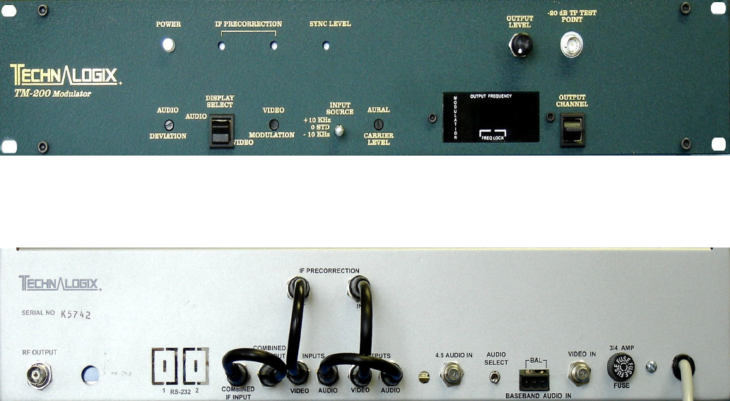
Location and Function of Controls and Connectors
The following illustrations depict the location of the installation connectors when
installing the power amplifier with a modulator or processor.
FRONT
BACK
Audio Deviation – Allows user to control extent of audio deviation. Original factory
setting at 25 KHz deviation using standard pre-emphasis curve.
Audio/Video Display Select - Provides a graphical representation of audio deviation and
visual modulation levels on an LED bar graph. The switch selects between audio
deviation or visual modulation.
Video Modulation -- Allows user to control extent of video modulation. Original factory
setting at 87.5% video modulation with 1.0 Volt peak to peak baseband input video
signal.
Frequency Offset Select – Toggles between +10 KHz, 0KHz, and –10 KHz frequency
offset.
TM-200 Issue 1.02 November 2005 Page 18 of 64
Aural Carrier Level - Allows user to set aural carrier level relative to visual carrier level.
Modulator is factory tested at –10 dBc (decibels below visual carrier).
Output Select – Selects the desired channel of operation. If you require a lower channel
than the one currently displayed, push the toggle switch down. The channels will
change one at a time as many times as you press the switch. Holding the select switch
in the up or down position will “scan” to the desired channel. It is normal for the
frequency lock LED to turn off during and for a few seconds after, changing channels.
The switch must be held up or down initially for three seconds. This helps to ensure that
no accidental channel changes will occur.
Output Level – Sets visual carrier output level.
RF Out Test Point – Provides a sample of the RF output level which is 20 dB below the
actual value. RF test point is only a relative indicator of the actual RF output level and
may vary. All RF operating measurements should be made at the RF output of the unit.
RF Output - Modulated Audio/ Video output capable of +60 dBmV levels using built in
low distortion hybrid amplifiers.
RS-232 Ports – Set up for optional RS-232 control option.
Combined IF Input/ Output – 45.75 MHz visual carrier and 41.25 MHz audio carrier
intermediate frequency signal loop.
Audio Input/ Ouput Loop – Available for baseband audio processing.
Video Input/ Output Loop - Available for baseband video processing.
IF Pre-Correction Loop – Allows pre-correction adjustment to improve linearity,
intermodulation performance, and other RF parameters. Internally connected to Signal
Conditioning PCB.
Video In – Connection for 1.0 Volt peak to peak video source.
Balanced Baseband Audio In – Used to connect a 1 Volt peak to peak baseband audio
signal. For balanced input connection, connect 1 audio input lead to the left terminal on
the connector and the other audio input lead to the right terminal. For an unbalanced
input connection, connect one audio input lead to the left terminal on the connector and
the other audio input lead to the centre terminal. The center terminal is chassis ground.

TM-200 Issue 1.02 November 2005 Page 19 of 64
5.0
O
PERATING
P
ROCEDURE
Preliminary Hook-up
1. Terminate modulator into a 50 ohm load before applying power.
2. Connect the power cord of the Technalogix TM-200 agile modulator to a proper
electrical source as indicated on the back of the unit.
3. Observe the front panel. If power is applied and present, the red power LED will
illuminate. Also, all the elements of the displays behind the display readout
window will illuminate momentarily as a display test.
4. Observe the numbers displayed behind the display readout window after the test.
They will indicate:
• Microprocessor software version;
• Internal option dipswitch settings;
• RS-232 unit ID (if so equipped); and
• Last tuned channel.
5. After a moment, the Lock Detect LED will illuminate.
TM-200 Issue 1.02 November 2005 Page 20 of 64
Setup of Output Level and Channel Selection
1. Connect a spectrum analyzer, or a field strength meter tuned to the frequency of
the video RF carrier of the desired channel, to the RF OUTPUT jack on the rear
panel of the unit. Alternatively, connect a spectrum analyzer or a field strength
meter to the –20dB TEST POINT on the front panel of the unit.
2. Select the desired output channel using the CHANNEL SELECT paddle switch
on the front panel.
• Hold the CHANNEL SELECT switch in the up- or down-position for
approximately 3 seconds to activate the channel-select circuit;
• Toggle the CHANNEL SELECT switch up to select a higher channel
or toggle it down to select a lower channel. The switch may be held in
the up- or down-position for rapid channel switching.
3. Observe the output on the spectrum analyzer, or the field strength meter. If
measuring from the rear panel RF OUTPUT jack, adjust the front panel OUTPUT
LEVEL potentiometer for an output level between +55dBmV and +60dBmV. If
measuring from the front panel –20dB TEST POINT, ensure that the rear panel
RF OUTPUT jack is terminated into a 50Ω load, then adjust the front panel
OUTPUT LEVEL potentiometer for an output level between +35dBmV and
+40dBmV.
4. If using a field strength meter, retune the meter to the frequency of the audio RF
Carrier.
5. Still observing the output on the spectrum analyzer, or the field strength meter
(now tuned to the frequency of the audio RF carrier), adjust the front panel
AURAL CARRIER potentiometer for an output level 10-13dB lower than that at
which the video RF Carrier is set.
6. Remove the spectrum analyzer, or field strength meter from the unit. If available,
connect a television/monitor to the front panel –20dB TEST POINT, apply power
to the television/monitor and tune to the selected output channel of the
Technalogix TM-200 modulator.
TM-200 Issue 1.02 November 2005 Page 21 of 64
Setup of Video Input Connection and Adjustment
1. Connect a 1.0V
P-P
video source to the VIDEO IN jack on the rear panel.
2. Adjust the front panel VIDEO MODULATION control for 87.5% modulation.
• Set the front panel DISPLAY SELECT switch to VIDEO (down)
position;
• Observe front panel LED bar graph behind front panel display readout
window.
• First RED LED will begin illumination at approximately 87.5%
modulation; or
• Observe TV monitor for good visual image.
TM-200 Issue 1.02 November 2005 Page 22 of 64
Setup of Baseband Audio Input Connection and Adjustment
1. If your Technalogix TM-200 agile modulator is equipped with a 4.5MHz sub-
carrier input option, ensure that the rear-panel AUDIO SELECT switch is in the
BASEBAND position.
2. Connect a 1V
P-P
baseband audio signal to the rear panel baseband audio
connector as follows:
• For balanced input connection, connect one audio input lead to the
left terminal on the connector and the other audio input lead to the
right terminal.
• For unbalanced input connection, connect one audio input lead to the
left terminal on the connector and the other audio input lead to the
center terminal.
• Center terminal is chassis ground.
• Insert the terminal into the connector on the rear panel of the TM-200.
3. Adjust the front panel AUDIO MODULATION control for 100% modulation.
• Set the front panel DISPLAY SELECT switch to AUDIO (up) position.
• Observe front panel LED bar graph behind front panel display readout
window.
• First RED LED will begin illumination at approximately 95%
modulation; or
• Adjust for ±25KHz deviation using a spectrum analyzer; or
• Listen to the audio output from TV monitor and setting the loudness
equal to that of an off-air channel carried on your system.
TM-200 Issue 1.02 November 2005 Page 23 of 64
Setup of 4.5 MHz Sub-Carrier Audio Input Connection and Adjustment
1. Set the rear panel AUDIO SELECT switch in the 4.5 position.
2. Connect a modulated 4.5MHz sub-carrier signal to the rear panel 4.5MHz input
F-connector jack.
3. Inject a minimum +36dBmV (-12.75dBm) 4.5MHz RF carrier into the unit.
4. Using the setup in Step 5, Setup of Output Level and Channel Selection,
measure the audio RF carrier output level at the rear panel RF OUTPUT jack.
Level should be within ±2dB of the measurement taken in Step 5, Setup of
Output Level and Channel Selection.

TM-200 Issue 1.02 November 2005 Page 24 of 64
Setup of IF Pre-Correction on Signal Conditioning PCB
1. Install the modulator but do not apply power yet.
2. Ensure that the two IF pre-correction potentiometers on the front panel of the
modulator are turned fully counter clockwise.
3. With the transmitter and modulator fully installed, apply power and bring the
transmitter up to rated power.
4. Apply a red field test signal to the input of the modulator with the aural carrier
turned on.
5. Take a sample of the RF output and view it on a spectrum analyzer.
6. Looking at the +/- 920kHz intermodulation products, adjust the two IF pre-
correction potentiometers to obtain the lowest level on the intermodulation
products.
Varying these two pots can increase and dec
rease the
output power, so this should be carefully monitored.

TM-200 Issue 1.02 November 2005 Page 25 of 64
Setup of Sync Level on Signal Conditioning PCB
1. With the transmitter at rated power and an NTC7 Composite signal applied
to the input of the modulator, view the demodulated waveform on a waveform
monitor.
2. Adjust the sync level potentiometer on the front panel clockwise for more sync or
counter clockwise for less sync to obtain 40 IRE of sync.
3. Maintain the white bar level at 100 IRE by adjusting the video modulation
potentiometer on the front panel.
Varying these two pots can increase and decrease the
output power, so this should be carefully monitored.
TM-200 Issue 1.02 November 2005 Page 26 of 64
Automatic Shut Down
Technalogix power supplies are designed so that under certain power line or heat
buildup conditions, the unit shuts off. An indicator would be no RF output, but the
POWER LED remains on. If this occurs, unplug the power cord and wait two minutes
before re-powering. Upon applying power, you should again have RF output. If not, or
should the unit return to shutdown mode, please contact Technalogix for assistance.
Technalogix highly recommends a 1.75 inch air circulation space between any rack
mounted equipment.

TM-200 Issue 1.02 November 2005 Page 27 of 64
Transmitter Hookup
1. Connect modulated video from TM-200 RF OUT to the Technalogix power amplifier.
2. Turn down RF level on TM-200 all the way.
3. Ensure that IF OUT is connected to IF IN on the TM-200 modulator using the loop F
to F cable supplied. If the IF pre-correction circuit is to be used, simply jumper 75-
ohm coaxial from the IF PRE-CORRECTION - IN to the OUTPUTS – VIDEO and
jumper from IF PRE-CORRECTION – OUT to the INPUTS – VIDEO connection.
4. Connect the transmitting antenna cable to the RF output connector on the power
amplifier. It is recommended that a quality through line wattmeter be installed in this
same line.
5. Verify that all signal and RF cables are connected properly.
6. After following proper installation procedures outlined in the power amplifier manual,
plug the power amplifier’s power cords into an appropriate electrical outlet.
Output power should be adjusted with a sync and blanking signal only with the aural
carrier removed. This is simply done by disconnecting one end of the audio carrier loop
found on the back panel of the TM-200.

TM-200 Issue 1.02 November 2005 Page 28 of 64
6.0
P
ROBLEM
T
ROUBLESHOOTING
G
UIDE
The guide below covers some typical symptoms, possible associated causes and
suggested actions to follow before returning the unit for repair. It is not meant to be all-
inclusive.
Symptom Possible Cause Suggested Action
No output or weak output Baseband input level too weak Ensure proper 1 Vp-p video signal
present on input
IF loop cable on rear of unit loose
or disconnected
Check IF loop cable is securely
attached
Unit not plugged in or getting AC
power
Check power cord and power source,
fuse
Unit tuned to output channel
different from desired (this occurs
particularly on the units which
have green LED on the front
panel to indicate “T” channels and
channels above 99)
Ensure selected output channel is
desired channel
Loss of video on the input – video
detect turned off RF Output
Ensure proper 1 Vp-p video signal
present on input
Excessive noise or spurious
signals
Output level above rated
maximum (most often occurs
when changing from high-number
channel to low-number channel,
especially to the “T” channels)
Measure RF output from rear
panel jack and adjust front panel
OUTPUT LEVEL control as
required
IF level too high (most often
occurs when routing IF through
scrambler or other external
device)
Measure normal IF output level
for applied CW/unmodulated input
carrier and ensure same level is
returned to unit after external
processing
Input signal too strong or no input
signal at all
Measure video level and pad to
within specified input levels.
Bad/noisy video Aural carrier interfering with video
carrier
Measure Aural Carrier level
and/or adjust AURAL CARRIER
LEVEL control on front panel
Channels do not change Delay feature active Hold channel change switch in
raised/lowered position for at least
three seconds

TM-200 Issue 1.02 November 2005 Page 29 of 64
7.0
B
ILL OF
M
ATERIALS
,
S
CHEMATICS
,
AND
PCB
O
VERLAYS
Agile Logic Board Bill of Materials
Last Revision: 09.12.00
Component Reference Quantity
Identification Modifier Package
C1 1 22pF CAP250D
C10 1 0.47uF CAP100RP
C11 1 10 uF CAP100RP
C12 1 22 uF CAP100RP
C13 1 22 uF CAP100RP
C14 1 22 uF CAP100RP
C15 1 22 uF CAP100RP
C16 1 0.01uF CAP250D
C17 1 0.01uF CAP250D
C18 1 47 uF CAP100RP
C19 1 47 uF CAP100RP
C2 1 22pF CAP250D
C20 1 CAP100RP
C21 1 0.01uF CAP250D
C22 1 0.01uF CAP250D
C23 1 0.01uF CAP250D
C24 1 0.01uF CAP250D
C3 1 22 uF CAP100RP
C4 1 10 uF CAP100RP
C5 1 0.47uF CAP100RP
C6 1 0.47uF CAP100RP
C7 1 0.01uF CAP250D
C8 1 0.01uF CAP250D
C9 1 470 uF CAP197R
D1 1 RED T1 LED T1-W/HLD
D2 1 T1 W/HLD LED
D3 1 RED T1 LED T1-W/HLD
DS1 1 8 POS DPS8W
JP1 1 4 POS HEADER
JP-DUAL4
JP2 1 8 POS HEADER
JP-DUAL8
JP3 1 JP-DUAL4
JP4 1 3PIN JP3IL
JP5 1 3PIN JP3IL
JP6 1 3PIN JP3IL
JP7 1 3 POS JP3IL
JP8 1 3 IL JP3IL
L1 1 6 T COIL 60

TM-200 Issue 1.02 November 2005 Page 30 of 64
L2 1 6 T COIL 60
L3 1 6 T COIL 60
L4 1 6 T COIL 60
L5 1 6 T COIL 60
P1 1 4 PIN SMB
P10 1 10 POS DIPIL10
P11 1 4 PIN SMB
P12 1 8 POS CONNIL8
P2 1 RT ANG F FCONN
P3 1 12 POS CONN IL12
P4 1 12 POS CONN IL12
P5 1 ON DISPLAY
BDS
CONN IL19
P6 1 12 POS CONN IL12
P7 1 12 POS CONN IL12
P8 1 4 PIN SMB
P9 1 10 PIN CONN10IL
Q1 1 2222 TRANS2222
Q2 1 2907 TO18C
QP1 1 4-2222A DIP14C
R1 1 10 Mohm RES1-8
R10 1 1 kOhm RES1-8
R11 1 5 kOhm POT1
R12 1 10 Kohm RES1-8
R13 1 10 Kohm RES1-8
R14 1 1 kOhm RES1-8
R15 1 6.8 kOhm RES1-8
R16 1 1 kOhm RES1-8
R17 1 500 Ohm POT1
R18 1 10 Kohm RES1-8
R19 1 5.6 kOhm RES1-8
R2 1 4.7 Ohm RES1-8
R20 1 10 Kohm RES1-8
R21 1 91 Ohm RES1-8
R22 1 10 Ohm RES1-8
R23 1 5 kOhm POT1
R3 1 5 kOhm POT1
R4 1 10 Kohm RES1-8
R5 1 1 kOhm RES1-8
R6 1 68 kOhm RES1-8
R7 1 68 kOhm RES1-8
R8 1 68 kOhm RES1-8
R9 1 4.7 Ohm RES1-8
RP1 1 10 Kohm DIPIL11
RP2 1 10 Kohm DIPIL11
RP3 1 10 Kohm DIPIL11
RP4 1 150 Ohm DIP IL8
RP5 1 150 Ohm DIP IL8

TM-200 Issue 1.02 November 2005 Page 31 of 64
SW1 1 PADDLE SW1
SW2 1 PADDLE SW1
SW3 1 ROCKER SW1
SW4 1 ROCKER SW1
U1 1 MC74HC165 DIP16C
U2 1 IC34064 REGTO92
U3 1 68705C8 DIP40C
U4 1 74H04 DIP14C
U5 1 74H04 DIP14C
U6 1 MC14499 DIP18C
U7 1 DS232 DIP16C
U8 1 X2402 DIP8C
Y1 1 4MHz XTAL
TM-200 Issue 1.02 November 2005 Page 32 of 64
TM-200 Issue 1.02 November 2005 Page 33 of 64

TM-200 Issue 1.02 November 2005 Page 34 of 64
Agile Output Amplifier Bill of Materials
Last Revision: 09.12.00
Component Reference Quantity
Identification Modifier Package
C1 1 0.1uF 1206
C2 1 0.1uF 1206
C3 1 2.7 pF 1206
C4 1 3-10pF VCAP CGKG27
C5 1 3-10pF VCAP CGKG27
C6 1 3-10pF VCAP CGKG27
C7 1 2.7 pF 1206
E1 1 E-COAX
E2 1 12 V EPAD
E3 1 E-COAX
E5 1 GND EPAD
I1 1 1206
L1 1 IND400
L2 1 10 nH 1210
L3 1 12 nH 1210
L4 1 12 nH 1210
L5 1 10 nH 1210
P1 1 FCONN-S
U1 1 AMP6342
TM-200 Issue 1.02 November 2005 Page 35 of 64
TM-200 Issue 1.02 November 2005 Page 36 of 64

TM-200 Issue 1.02 November 2005 Page 37 of 64
Audio Video Modulator Board Bill of Materials
Last Revision: 09.12.00
Component
Reference
Quantity
Identification Modifier Package
C1 1 0.1uF SMD1206
C10 1 0.1uF SMD1206
C100 1 4.7uF CAP100RP
C101 1 100pF SMD1206
C102 1 47uF CAP100RP
C103 1 0.1uF SMD1206
C104 1 470pF SMD1206
C105 1 0.1uF SMD1206
C106 1 470uF CAP200RP
C107 1 0.1uF SMD1206
C108 1 470uF CAP200RP
C109 1 0.0027uF SMD1206
C11 1 0.1uF SMD1206
C110 1 0.1uF SMD1206
C111 1 NI SMD1206
C112 1 470uF CAP200RP
C113 1 0.1uF SMD1206
C114 1 0.1uF SMD1206
C115 1 0.1uF SMD1206
C116 1 0.1uF SMD1206
C117 1 0.01uF SMD1206
C118 1 18pF SMD1206
C119 1 NI SMD1206
C12 1 0.01uF SMD1206
C120 1 0.1uF SMD1206
C121 1 470uF CAP200RP
C122 1 0.01uF SMD1206
C123 1 470uF CAP200RP
C124 1 10pF SMD1206
C125 1 27pF SMD1206
C126 1 82pF SMD1206
C127 1 0.001uF SMD1206
C128 1 0.01uF SMD1206
C129 1 0.01uF SMD1206
C13 1 0.1uF SMD1206
C130 1 0.1uF SMD1206
C131 1 NI SMD1206
C132 1 0.1uF SMD1206
C133 1 0.01uF SMD1206
C134 1 0.01uF SMD1206

TM-200 Issue 1.02 November 2005 Page 38 of 64
C135 1 0.1uF SMD1206
C136 1 0.1uF SMD1206
C137 1 0.01uF SMD1206
C138 1 0.1uF SMD1206
C139 1 0.01uF SMD1206
C14 1 0.001uF SMD1206
C140 1 0.01uF SMD1206
C141 1 0.01uF SMD1206
C142 1 0.1uF SMD1206
C143 1 12pF SMD1206
C144 1 12pF SMD1206
C145 1 3-10pF CGKG27
C146 1 12pF SMD1206
C147 1 12pF SMD1206
C148 1 0.1uF SMD1206
C149 1 0.01uF SMD1206
C15 1 0.01uF SMD1206
C150 1 0.1uF SMD1206
C151 1 27pF SMD1206
C152 1 56pF SMD1206
C153 1 27pF SMD1206
C154 1 0.01uF SMD1206
C155 1 0.01uF SMD1206
C156 1 0.01uF SMD1206
C16 1 0.1uF SMD1206
C17 1 22pF SMD1206
C18 1 56pF SMD1206
C19 1 10pF SMD1206
C2 1 0.1uF SMD1206
C20 1 0.001uF SMD1206
C21 1 0.47uF SMD1206
C22 1 22pF SMD1206
C23 1 22pF SMD1206
C24 1 4.5-20pF CGKG27
C25 1 0.01uF SMD1206
C26 1 0.001uF SMD1206
C27 1 22pF SMD1206
C28 1 4.7uF CAP100RP
C29 1 100pF SMD1206
C3 1 4.7uF CAP100RP
C30 1 0.01uF SMD1206
C31 1 0.1uF SMD1206
C32 1 0.001uF SMD1206
C33 1 0.01uF SMD1206
C34 1 68pF SMD1206
C35 1 100pF SMD1206
C36 1 100pF SMD1206
C37 1 68pF SMD1206

TM-200 Issue 1.02 November 2005 Page 39 of 64
C38 1 470uF CAP200RP
C39 1 0.01uF SMD1206
C4 1 0.1uF SMD1206
C40 1 0.01uF SMD1206
C41 1 0.1uF SMD1206
C42 1 0.01uF SMD1206
C43 1 0.01uF SMD1206
C44 1 0.1uF SMD1206
C45 1 470uF 25V CAP200RP
C46 1 1000uF CAP300RP
C5 1 4.7uF CAP100RP
C6 1 0.1uF SMD1206
C7 1 0.001uF SMD1206
C8 1 470uF CAP200RP
C9 1 47pF SMD1206
D1 1 5236 SOT23
D10 1 3800 SOT23
D100 1 2800 SOT23
D101 1 2800 SOT23
D11 1 3800 SOT23
D2 1 2800 SOT23
D3 1 2800 SOT23
D6 1 MMBV105GL SOT23
D7 1 10 V SOT23
D8 1 4.7V SOT23
D9 1 3800 SOT23
F1 1 SIP5L
F100 1 FILTER2219
F101 1 SF28S
J1 1 NI SMD1206
JP1 1 NI SMD1206
JP2 1 0 SMD1206
JP3 1 NI SMD1206
JP4 1 NI SMD1206
JP5 1 0 SMD1206
L1 1 10.5 T,26GA COIL
L100 1 12.5T 22GA COIL
L101 1 0.47uH SMD1812
L102 1 0.47uH SMD1812
L103 1 12.5T 22GA COIL-S
L104 1 12.5T 22GA COIL-S
L105 1 0.47uH SMD1812
L106 1 0.47uH SMD1812
L107 1 0.47uH SMD1812
L15 1 0.47uH IND400
L2 1 0.33uH SMD1812
L3 1 0.33uH SMD1812
L4 1 0.33uH SMD1812

TM-200 Issue 1.02 November 2005 Page 40 of 64
L5 1 0.47uH SMD1812
MX100 1 MIXER
P1 1 FCONN-S
P100 1 FCONN-S
P101 1 RTARCA
P102 1 RTARCA
P103 1 FCONN-S
P2 1 CONN10IL
P7 1 CONHDR6
P8 1 CONHDR6
Q1 1 2369 SOT23
Q100 1 2222 SOT23
Q101 1 2907 SOT23
Q102 1 2222 SOT23
Q103 1 2222 SOT23
Q104 1 2907 SOT23
Q105 1 2222 SOT23
Q106 1 2222 SOT23
Q107 1 2222 SOT23
Q108 1 MRF559B2
Q109 1 MRF559B2
Q110 1 MRF559B2
Q2 1 2369 SOT23
R1 1 300kohm SMD1206
R10 1 220kohm SMD1206
R100 1 75ohm R1206A
R101 1 22kohm SMD1206
R102 1 270ohm SMD1206
R103 1 620ohm SMD1206
R104 1 2kohm SMD1206
R105 1 360ohm SMD1206
R106 1 2kohm SMD1206
R107 1 51ohm SMD1206
R108 1 330ohm SMD1206
R109 1 3.6kohm SMD1206
R11 1 100ohm SMD1206
R110 1 6.8kohm SMD1206
R111 1 680kohm SMD1206
R112 1 1kohm SMD1206
R113 1 910ohm SMD1206
R114 1 22ohm SMD1206
R115 1 330ohm SMD1206
R116 1 1.5kohm SMD1206
R117 1 560ohm SMD1206
R118 1 1kohm SMD1206
R119 1 330ohm SMD1206
R12 1 75kohm SMD1206
R120 1 1kohm POTENTIOMETER ST53YJ

TM-200 Issue 1.02 November 2005 Page 41 of 64
R121 1 560ohm SMD1206
R122 1 1.5kohm SMD1206
R123 1 470kohm SMD1206
R124 1 51ohm SMD1206
R125 1 10kohm POTENTIOMETER ST53YJ
R126 1 1kohm SMD1206
R127 1 1kohm SMD1206
R128 1 NI SMD1206
R129 1 360ohm SMD1206
R13 1 1kohm SMD1206
R130 1 10kohm POTENTIOMETER ST53YJ
R131 1 180ohm SMD1206
R132 1 51ohm SMD1206
R133 1 150ohm SMD1206
R134 1 22ohm SMD1206
R135 1 10kohm SMD1206
R136 1 10kohm SMD1206
R137 1 1.5kohm SMD1206
R138 1 1kohm SMD1206
R139 1 10kohm SMD1206
R14 1 470kohm SMD1206
R140 1 20kohm 1% SMD1206
R141 1 27ohm SMD1206
R142 1 36ohms SMD1206
R143 1 27ohm SMD1206
R144 1 1kohm SMD1206
R145 1 4.7ohm SMD1206
R146 1 82ohm SMD1206
R147 1 2kohm SMD1206
R148 1 220ohm SMD1206
R149 1 75ohm SMD1206
R15 1 10kohm POTENTIOMETER ST53YJ
R150 1 1kohm SMD1206
R151 1 18ohm SMD1206
R152 1 1kohm SMD1206
R153 1 1kohm SMD1206
R154 1 2kohm SMD1206
R155 1 4.7ohm SMD1206
R156 1 82ohm SMD1206
R157 1 220ohm SMD1206
R158 1 75ohm SMD1206
R159 1 4.7ohm SMD1206
R16 1 100ohm SMD1206
R160 1 91ohm SMD1206
R161 1 4.7ohm SMD1206
R162 1 4.7ohm SMD1206
R163 1 75ohm SMD1206
R164 1 4.7ohm SMD1206

TM-200 Issue 1.02 November 2005 Page 42 of 64
R165 1 1kohm SMD1206
R166 1 2kohm SMD1206
R167 1 4.7ohm SMD1206
R168 1 82ohm SMD1206
R169 1 75ohm SMD1206
R17 1 1kohm SMD1206
R170 1 220ohm SMD1206
R171 1 NI SMD1206
R172 1 NI SMD1206
R18 1 270ohm SMD1206
R19 1 10kohm SMD1206
R2 1 150kohm SMD1206
R20 1 560ohm SMD1206
R21 1 10kohm SMD1206
R22 1 1kohm SMD1206
R23 1 390ohm SMD1206
R24 1 100kohm SMD1206
R25 1 220kohm SMD1206
R26 1 1Mohm SMD1206
R27 1 2kohm SMD1206
R28 1 68ohm RES2010A
R29 1 220ohm 1/2 WATT RES2010A
R3 1 300kohm SMD1206
R30 1 75ohm SMD1206
R31 1 1kohm SMD1206
R32 1 1kohm SMD1206
R33 1 2kohm SMD1206
R34 1 1kohm SMD1206
R35 1 4.7kohm SMD1206
R36 1 2kohm SMD1206
R37 1 1kohm SMD1206
R38 1 430ohm SMD1206
R39 1 27ohm SMD1206
R4 1 150kohm SMD1206
R40 1 430ohm SMD1206
R5 1 1kohm SMD1206
R7 1 4.7kohm SMD1206
R8 1 10kohm SMD1206
R9 1 10kohm SMD1206
TB1 1 TERBLK
TP100 1 0 SMD1206
TP101 1 0 SMD1206
U1 1 LF353 DIP8SM
U100 1 NE592D DIP8SM
U101 1 2090 DIP16SM
U102 1 LM1881 DIP8SM
U103 1 LM358 DIP8SM
U2 1 145106 145106

TM-200 Issue 1.02 November 2005 Page 43 of 64
U4 1 501 FPT-08-M01
Y1 1 XTL49
Y100 1 45.75Mhz XTL49
TM-200 Issue 1.02 November 2005 Page 44 of 64
TM-200 Issue 1.02 November 2005 Page 45 of 64

TM-200 Issue 1.02 November 2005 Page 46 of 64
Signal Conditioning Bill of Materials
Last Revision: 11.07.05
Index
Qty
Designations Description Mfg. Part Number Package
1 1 C832 Capacitor, electrolytic, 10uF 35V ECE-V1VA100SR VS "C"
2 2 C839, C840 Capacitor, electrolytic, 100uF, 25V, SMD ECE-V1EA101UP VS 'E'
3 1 C817 Capacitor, electrolytic, 100uF, 10V, SMD ECE-V1AA101SP VS 'D'
4 4
C803, C806,
C809, C815 Capacitor, tantalum, 10uF, 16V, SMD T491B106K016AS SMD 3528
5 1 C820 Capacitor, ceramic, 470pF 50V X7R CC0805KRX7R9BB471 SMD 0805
6 10
C821, C824,
C825, C826,
C827, C828,
C829, C830,
C833, C834 Capacitor, ceramic, 1000pF 50V, X7R 10% ECJ-2VB1H102K SMD 0805
7 10
C802, C805,
C808, C814,
C818, C823,
C831, C835,
C836, C837 Capacitor, ceramic, 0.01uF 50V X7R C0805C103K5RACTU SMD 0805
8 9
C801, C804,
C807, C810,
C811, C812,
C813, C816,
C819 Capacitor, ceramic, 0.1 uF, 50V, SMD C0805C104K5RACTU SMD 0805
9 1 C838 Capacitor, ceramic, 0.33 uF, 25V, SMD ECJ-2YF1E334Z SMD 0805
10 1 C822 Capacitor, trim 5-50pF low power 9410-5SL-1 SMD
11 1 D801 Diode, 200mA, 100V, SMD SOT-23
12 1 D802 Diode Sil 2A 200V DO-214AA S2D SMBJ
13 2 D803, D804 Diode, If= 1A, Vbr= 100V SOT-23
14 1 D805 Diode, LED, 5mm, 1500mCd SSL-LX5093SRC/DV TH
15 1 J801 Connector, 4-position, 0.2" spacing, rt. angle ED120/4DS 0.2" THT
16 2 J802, J803 Connector, RCA, jack, vertical, PC mount, blue RCJ-021
J804, J805 Connector, F, PCB, strait RFF-1450-03 TH
17 1 K801 Relay, DPDT, 5Vdc coil TX2SA-5V SMD
18 5
L801, L802,
L803, L804,
L805 Inductor, 0.01uH, 0.450A max NLV32T-010J-PF SMD 1210
19 1 L806 Inductor, 1.5uH, 5% KL32LTE1R5J SMD 1210
20 2 L807, L808 Inductor, 2.2uH, 5% KL32LTE2R2J SMD 1210
21 4
Q801, Q802,
Q803, Q804 Transistor, general purpose SOT-23
22 2 R830, R831 Resistor, 0.0Ω, 5% 9C12063A0R00JLHFT SMD 1206
23 2 R821, R822 Resistor, 39Ω, 1% MCR10EZHF39R0 SMD 0805
24 1 R826 Resistor, 56Ω, 1% MCR10EZHF56R0 SMD 0805
25 1 R819 Resistor, 68Ω, 1% MCR10EZHF68R0 SMD 0805
26 2 R808, R818 Resistor, 75 ohm, 1/4W CRCW1206-750JRT1 SMD 1206
27 1 R827 Resistor, 100Ω, 1% MCR10EZHF1000 SMD 0805
28 1 R820 Resistor, 100Ω, 5% ERJ-1TYJ101U SMD 2512
29 3
R801, R824,
R825 Resistor, 120 ohm, 1/8W MCR10EZHF1210 SMD 0805

TM-200 Issue 1.02 November 2005 Page 47 of 64
30 1 R823 Resistor, 120Ω, 5% MCR18EZHJ121 SMD 1206
31 2 R806,R807 Resistor, 402 ohm, 1/8W MCR10EZHF4020 SMD 0805
32 2 R803, R832 Resistor, 470 ohm, 1/8W MCR10EZHF4700 SMD 0805
33 1 R829 Resistor, 680Ω, 1% MCR10EZHF6800 SMD 0805
34 1 R813 Resistor, 1 kohm, 1/8W MCR10EZHF1001 SMD 0805
35 1 R828 Resistor, 1.8KΩ, 1% MCR10EZHF1801 SMD 0805
36 4
R811, R812,
R816, R817 Resistor, 3 kohm, 1/8W MCR10EZHF3001 SMD 0805
37 5
R802, R804,
R810, R814,
R815 Resistor, 10 kohm, 1/8W MCR10EZHF1002 SMD 0805
38 1 R809 Resistor, 47 kohm, 1/8W MCR10EZHF4702 SMD 0805
39 1 R805 Resistor, TBD, 1/8W ( Not stuffed) SMD 0805
40 1 S801 Square post header, 3 position, 0.1" breakaway
7000-1X25SG -
41 1 S802 Square post header, 2 position, 0.1" breakaway
42 1 U801 IC, video signal conditioner MAX7450 SOIC-8
43 2 U802, U803 IC, op-amp, voltage limiting OPA698ID SOIC-8
44 1 U804 IC, comparator, dual LM393M SOIC-8
45 1 U805 IC, voltage reference SOT-23
46 1 U806 Amplifier SMD
47 1 U807 IC, regulator, +5V, 500mA LM78M05CDT SMD
48 1 U808 IC, voltage converter, 100mA, 735mW LM2660M SOIC-8
49 1 VR801 Potentiometer, 10KΩ, 3/8" top adj. 3386P-1-103 TH
50 2 VR804, VR805 Potentiometer, 10KΩ, 4MM top adj. 3214W-1-103E SMD
51 2 VR802, VR803 Potentiometer, 500Ω, 3/8" top adj. 3386P-1-501 TH
52 1 PCB
Printed circuit board, double sided, FR4,
0.062", 3.359" (W) X 1.550" (H) -
53 3 Spacer, 1/4" Hex, Aluminum, M/F, 4-40 139213
54 1
Cable, RG-179/PP7.5", connects V.C.B. to
modulator 500-0010-045
TM-200 Issue 1.02 November 2005 Page 48 of 64
TM-200 Issue 1.02 November 2005 Page 49 of 64

TM-200 Issue 1.02 November 2005 Page 50 of 64
Digital Up converter Bill of Materials
Last Revision: 09.12.00
Component Reference
Quantity
Identification Modifier Package
C1 1 0.1uF 1206
C101 1 100 Pf 1206
C102 1 0.1uF 1206
C103 1 100uF 25V CAP100RP
C104 1 0.47uF 1812
C105 1 0.1uF 1206
C106 1 0.22uF 1206
C107 1 100 Pf 1206
C108 1 1pF 1206
C109 1 100 Pf 1206
C11 1 0.1uF 1206
C110 1 100 Pf 1206
C111 1 1pF 1206
C112 1 1pF 1206
C113 1 1pF 1206
C114 1 1pF 1206
C115 1 0.47uF 1812
C116 1 0.1uF 1206
C116A 1 100uF 25V CAP100RP
C117 1 0.1uF 1206
C118 1 0.1uF 1206
C119 1 0.1uF 1206
C12 1 0.01uF 1206
C120 1 100 Pf 1206
C126 1 0.1uF 1206
C127 1 0.1uF 1206
C128 1 100 Pf 1206
C129 1 0.1uF 1206
C13 1 0.1uF 1206
C130 1 2.2pF 1206
C131 1 100 Pf 1206
C132 1 0.1uF 1206
C133 1 0.47uF 1206
C134 1 100uF 25V CAP100RP
C135 1 10 Pf 1206
C136 1 10 Pf 1206
C137 1 10 Pf 1206
C138 1 10 Pf 1206
C139 1 10 Pf 1206
C14 1 0.01uF 1206
C140 1 10 Pf 1206
C141 1 NI 1206

TM-200 Issue 1.02 November 2005 Page 51 of 64
C15 1 0.1uF 1206
C2 1 0.01uF 1206
C201 1 NI CGKG27
C204 1 0.1uF 1206
C205 1 0.1uF 1206
C206 1 100 Pf 1206
C207 1 0.1uF 1206
C208 1 2.2pF 1206
C209 1 0.1uF 1206
C21 1 0.1uF 1206
C210 1 0.1uF 1206
C3 1 0.01uF 1206
C300 1 0.1uF 1206
C301 1 100 Pf 1206
C303 1 470 uF 25 V CAP200RP
C4 1 0.01uF 1206
C5 1 0.1uF 1206
D1 1 3800 SOT-23
D100 1 9.1V DIODEZ DO214AC
D101 1 9V 914 SOT-23
D102 1 4.7V SOT-23
D103 1 10 V DIODEZ DO214AC
D2 1 3800 SOT-23
D3 1 3800 SOT-23
F2 1 F-LP-TOKO
F4 1 F-LP-TOKO
FT200 1 FIL-TOKO
J1 1 N/A THRU-HOLE
J10 1 N/A THRU-HOLE
J2 1 N/A THRU-HOLE
J3 1 N/A THRU-HOLE
J4 1 N/A THRU-HOLE
J5 1 N/A THRU-HOLE
J6 1 N/A THRU-HOLE
J7 1 N/A THRU-HOLE
J8 1 N/A THRU-HOLE
J9 1 N/A THRU-HOLE
L1 1 0.47uH 1812
L104 1 10nH 1812
L107 1 0.22uH 1210
L108 1 0.22uH 1210
L109 1 0.22uH 1210
L5 1 0.47uH 1812
L6 1 0.47uH 1812
M1 1 MIXER-RF2
P1 1 N/A FCONN-S
P2 1 N/A FCONN-S
R1 1 1k Ohm 1206

TM-200 Issue 1.02 November 2005 Page 52 of 64
R101 1 1k Ohm 1206
R102 1 910 Ohm 1206
R103 1 910 Ohm 1206
R104 1 0 1206
R105 1 47 kOhm 1206
R106 1 220 Ohm 1/2 WATT RES2010A
R108 1 43 Ohm 1/2 WATTS RES2010A
R109 1 220 Ohm 1/2 WATT RES2010A
R111 1 33 Ohm 1206
R112 1 180 Ohm 1206
R113 1 180 Ohm 1206
R114 1 220 Ohm 1/2 WATT RES2010A
R115 1 75 Ohm 1206
R116 1 10 Ohm 1206
R117 1 36 Ohm 1206
R118 1 10 Ohm 1206
R119 1 75 Ohm 1206
R120 1 110 Ohm 1 WATT RES2010A
R121 1 4.7 Ohm 1206
R122 1 91 Ohm 1206
R123 1 4.7 Ohm 1206
R14 1 36 Ohm 1206
R15 1 62 Ohm 1206
R16 1 36 Ohm 1206
R17 1 1k Ohm 1206
R18 1 2k Ohm 1206
R19 1 75 Ohm 1206
R2 1 1k Ohm 1206
R20 1 8.2 Ohm 1206
R200 1 300 Ohm 1206
R201 1 18 Ohm 1206
R202 1 300 Ohm 1206
R203 1 100 Ohm 1206
R204 1 110 Ohm 1 WATT RES2010A
R205 1 4.7 Ohm 1206
R206 1 75 Ohm
1206
R207 1 4.7 Ohm 1206
R21 1 82 Ohm 1206
R22 1 220 Ohm 1206
R23 1 100 Ohm 1206
R24 1 4.7 Ohm 1206
R25 1 100 Ohm 1206
R3 1 2k Ohm 1206
R4 1 4.7k Ohm 1206
R5 1 2k Ohm 1206
R6 1 1k Ohm 1206
U100 1 145200 TSSOP20
U101 1 ERA5 WW107

TM-200 Issue 1.02 November 2005 Page 53 of 64
U102 1 ERA5 WW107
U2 1 RF559B2
U200 1 ERA5 WW107
VC01 1 MINI14SL
TM-200 Issue 1.02 November 2005 Page 54 of 64
TM-200 Issue 1.02 November 2005 Page 55 of 64

TM-200 Issue 1.02 November 2005 Page 56 of 64
750 MHz Down Converter Bill of Materials
Last Revision: 09.13.00
Component Reference
Quantity
Identification Modifier Package
C1 1 27 pF 1206
C10 1 100 pF 1206
C100 1 2.2 pF 1206
C101 1 2.2 pF 1206
C102 1 NI 1206
C11 1 0.1 uF 1206
C12 1 0.47 uF 1812
C13 1 100 uF 25 V CAP100RP
C14 1 NI 1206
C15 1 10 pF 1206
C16 1 10 pF 1206
C17 1 10 pF 1206
C18 1 10 pF 1206
C19 1 10 pF 1206
C2 1 27 pF 1206
C20 1 10 pF 1206
C200 1 NI 1206
C205 1 2.7 pF 1206
C206 1 3-10 pF CGKG27
C207 1 3-10 pF CGKG27
C208 1 3-10 pF CGKG27
C209 1 2.7 pF 1206
C21 1 0.1 uF 1206
C210 1 0.1 uF 1206
C211 1 0.1 uF 1206
C212 1 0.1 uF 1206
C213 1 100 pF 1206
C214 1 1 pF 1206
C215 1 10 pF 1206
C22 1 0.22 uF 1206
C23 1 100 pF 1206
C24 1 1 pF 1206
C25 1 100 pF 1206
C26 1 0.1 uF 1206
C27 1 100 uF 25 V CAP100RP
C28 1 0.1 uF 1206
C29 1 0.1 uF 1206
C3 1 4.5-20 pF CGKG27
C30 1 0.1 uF 1206
C301 1 0.1 uF 1206
C302 1 100 pF 1206
C303 1 470 uF 35 WV CAP275RP650

TM-200 Issue 1.02 November 2005 Page 57 of 64
C304 1 0.1 uF 1206
C31 1 1206
C33 1 1 pF 1206
C34 1 1 pF 1206
C35 1 1 pF 1206
C36 1 1 pF 1206
C37 1 0.1 uF 1206
C38 1 0.1 uF 1206
C39 1 NI 1206
C4 1 0.47 uF 1812
C40 1 NI 1206
C41 1 NI 1206
C44 1 0.1 uF 1206
C45 1 0.1 uF 1206
C46 1 100 pF 1206
C5 1 100 pF 1206
C6 1 0.1 uF 1206
C7 1 0.47 uF 1812
C8 1 100 uF 25 V CAP100RP
C9 1 100 pF 1206
D1 1 9 V D914 SOT23
D2 1 9.1 V DIODEZ D0214AC
D3 1 9 V SOT23
D4 1 DIODEZ D0214AC
FT100 1 FIL-TOKO
J1 1 THRU-HOLE
J2 1 THRU-HOLE
J3 1 THRU-HOLE
J4 1 THRU-HOLE
J5 1 THRU-HOLE
J6 1 THRU-HOLE
J7 1 THRU-HOLE
J8 1 THRU-HOLE
J9 1 THRU-HOLE
L1 1 0.22 uH 1210
L100 1 10 nH 1210
L2 1 0.22 uH 1210
L200 1 10 nH 1210
L201 1 12 nH 1210
L202 1 12 nH 1210
L203 1 10 nH 1210
L204 1 10 nH 1210
L3 1 0.22 uH 1210
L4 1 10 nH 1210
M1 1 PULSAR MIXER-RF2
OSC1 1 MA06 MINI14SL
P1 1 FCONN-S
P2 1 FCONN-S

TM-200 Issue 1.02 November 2005 Page 58 of 64
R10 1 180 Ohm 1206
R100 1 33 Ohm 1206
R101 1 51 Ohm 1206
R102 1 4.7 Ohm 1206
R103 1 91 Ohm 1206
R104 1 4.7 Ohm 1206
R11 1 33 Ohm 1206
R12 1 180 Ohm 1206
R13 1 220 Ohm 1/2 WATT RES2010A
R14 1 0 Ohm 1206
R15 1 75 Ohm 1206
R16 1 10 Ohm 1206
R17 1 33 Ohm 1206
R18 1 NI 1206
R19 1 NI 1206
R2 1 10 kOhm 1206
R20 1 4.7 Ohm 1206
R200 1 NI 1206
R201 1 NI 1206
R202 1 0 Ohm 1206
R203 1 NI 1206
R204 1 0 Ohm 1206
R207 1 0 Ohm 1206
R208 1 110 Ohm 1 WATT RES2010A
R209 1 0 Ohm 1206
R21 1 110 Ohm 1 WATT RES2010A
R210 1 NI 1206
R211 1 0 Ohm 1206
R22 1 75 Ohm 1206
R3 1 220 Ohm 1/2 WATT RES2010A
R4 1 47 kOhm 1206
R5 1 RES2010A
R6 1 910 Ohm 1206
R7 1 910 Ohm 1206
R8 1 0 Ohm 1206
R9 1 43 Ohm 1/2 WATT RES2010A
U1 1 145200 TSSOP20
U2 1 ERA3 WW107
U201 1 ERA5 WW107
U3 1 ERA5 WW107
Y1 1 4000 MHz XTL49
TM-200 Issue 1.02 November 2005 Page 59 of 64
TM-200 Issue 1.02 November 2005 Page 60 of 64

TM-200 Issue 1.02 November 2005 Page 61 of 64
Power Supply Bill of Materials
Last Revision: 09.12.00
Component
Reference
Quantity
Identification Modifier Package
C1 1 4700 35 V CAP400RPHORZ
C10 1 0.1 uF CAP250
C11 1 0.1 uF CAP250
C12 1 0.1 uF CAP250
C13 1 0.1 uF CAP250
C14 1 1000 50 V CAP275RP650
C15 1 0.1 uF CAP250
C16 1 4700 16 VDC CAP275RP650
C17 1 1000 50 V CAP275RP650
C18 1 0.1 uF CAP250
C19 1 0.1 uF CAP250
C2 1 4700 35 V CAP400RPHORZ
C3 1 0.1 uF CAP250
C4 1 0.1 uF CAP250
C5 1 0.1 uF CAP250
C6 1 0.1 uF CAP250
C7 1 2200 35 V CAP275RP650
C8 1 0.1 uF CAP250
C9 1 10000 25 VDC CAP400RPHORZ
P1 1 CONHDR6
P2 1 CONHDR6
P3 1 CONHDR6
P4 1 CONHDR6
P5 1 CONHDR6
P6 1 CONHDR6
P7 1 CONHDR8
R1 1 2 kOhm RES400
R2 1 240 Ohm RES400
R4 1 5.6 kOhm RES400
U1 1 BRIDGE
U2 1 RBRDG-RECT-
403M
U3 1 LM317 T0-220-AB
U4 1 7824 T0-220-AB
U5 1 7812 T0-220-AB
U6 1 7805 T0-220-AB
U7 1 DIP6-2
TM-200 Issue 1.02 November 2005 Page 62 of 64
TM-200 Issue 1.02 November 2005 Page 63 of 64