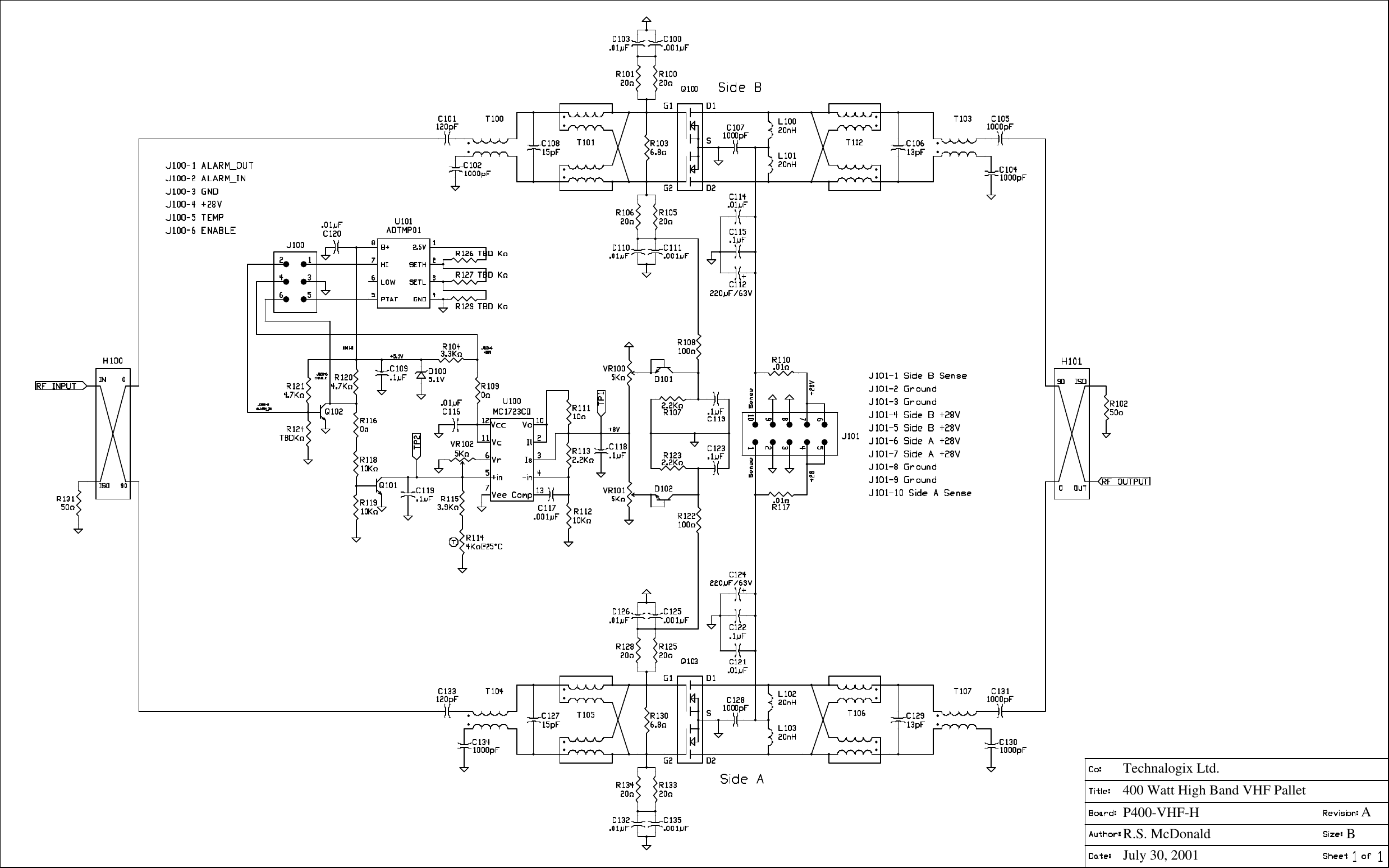
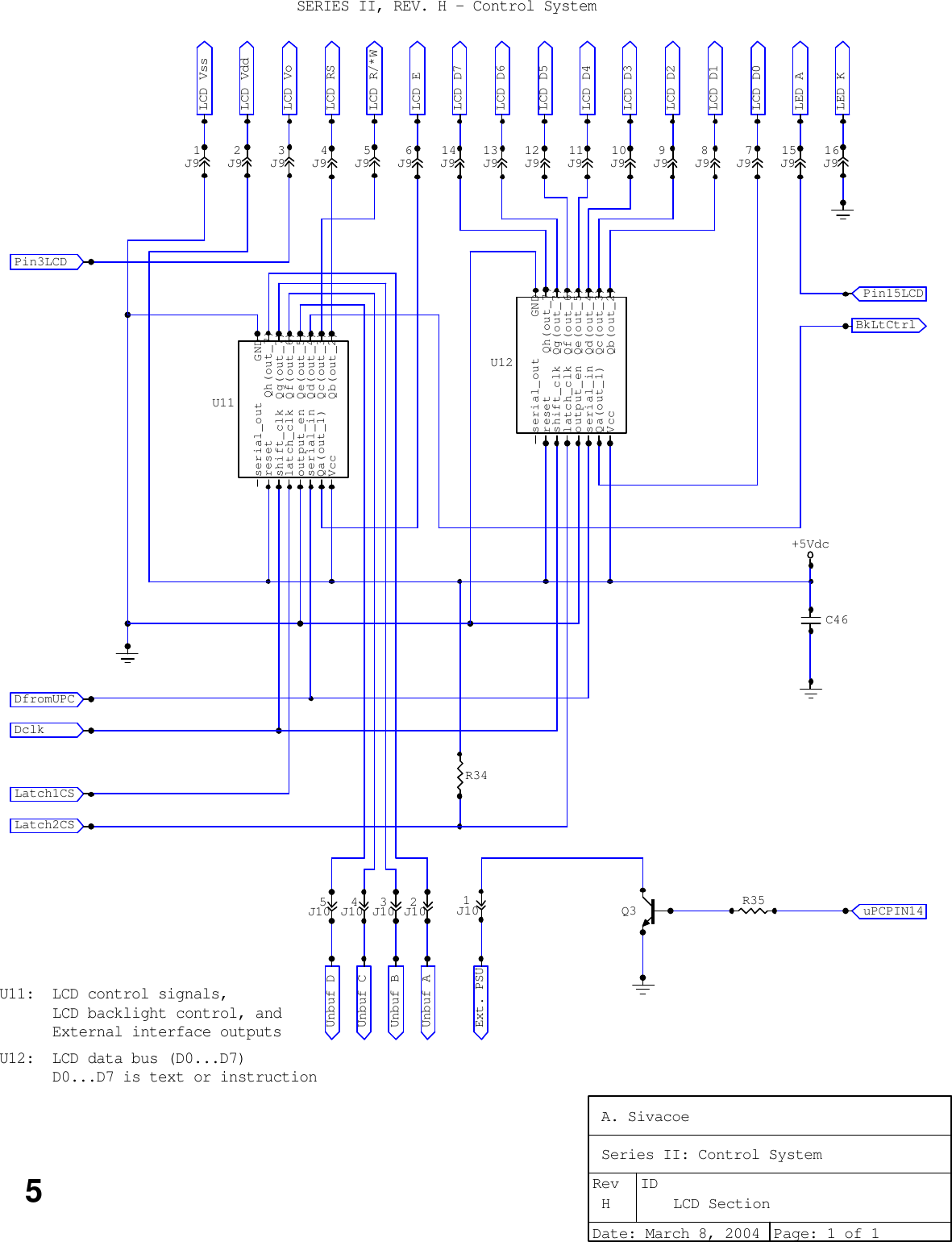
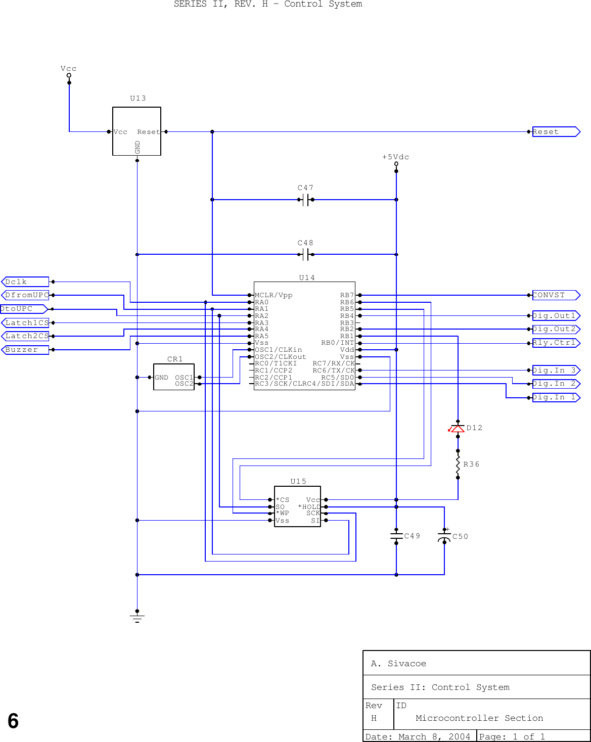
Technalogix TXV1000 TXV-1000 VHF Transmitter User Manual ContentsTAV1000
Technalogix, Ltd. TXV-1000 VHF Transmitter ContentsTAV1000
UserManual.wiki
>
Technalogix
>
TXV1000 User Manual
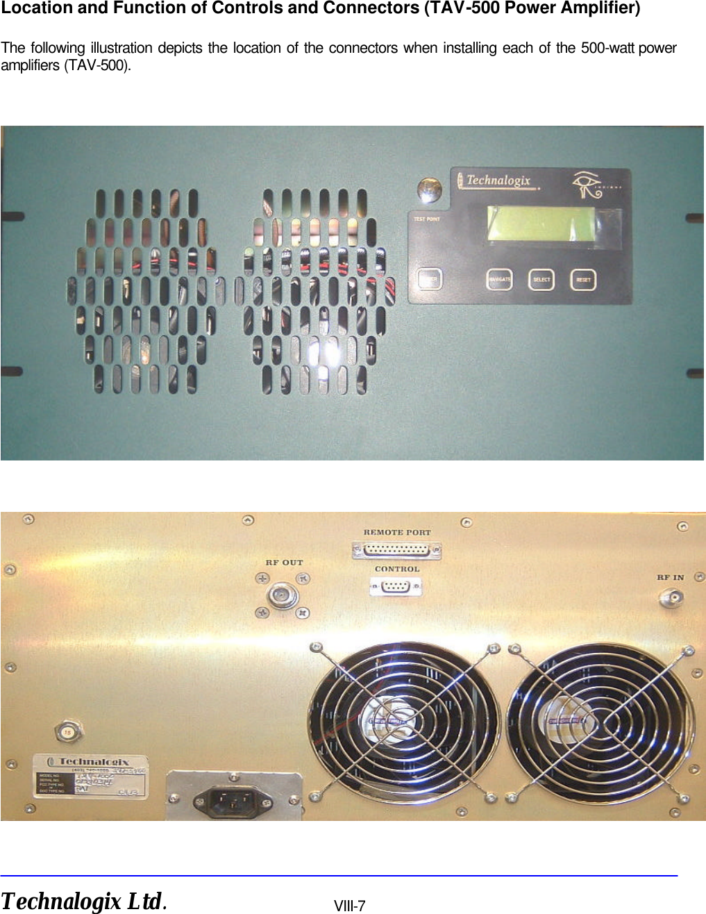
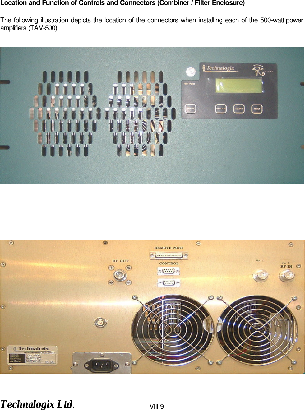
Manual-TAV1000
Navigation menu
Upload a User Manual
Namespaces
Wiki Guide
HTML
PDF
Info
Views
User Manual
Discussion / Help
Navigation