Telit Cinterion Deutschland XT55 Transmitter module for fixed / mobile applications User Manual XT55 56
Gemalto M2M GmbH Transmitter module for fixed / mobile applications XT55 56
Contents
- 1. Exhibit 8 User manual
- 2. Updated Usaer Manual
Updated Usaer Manual
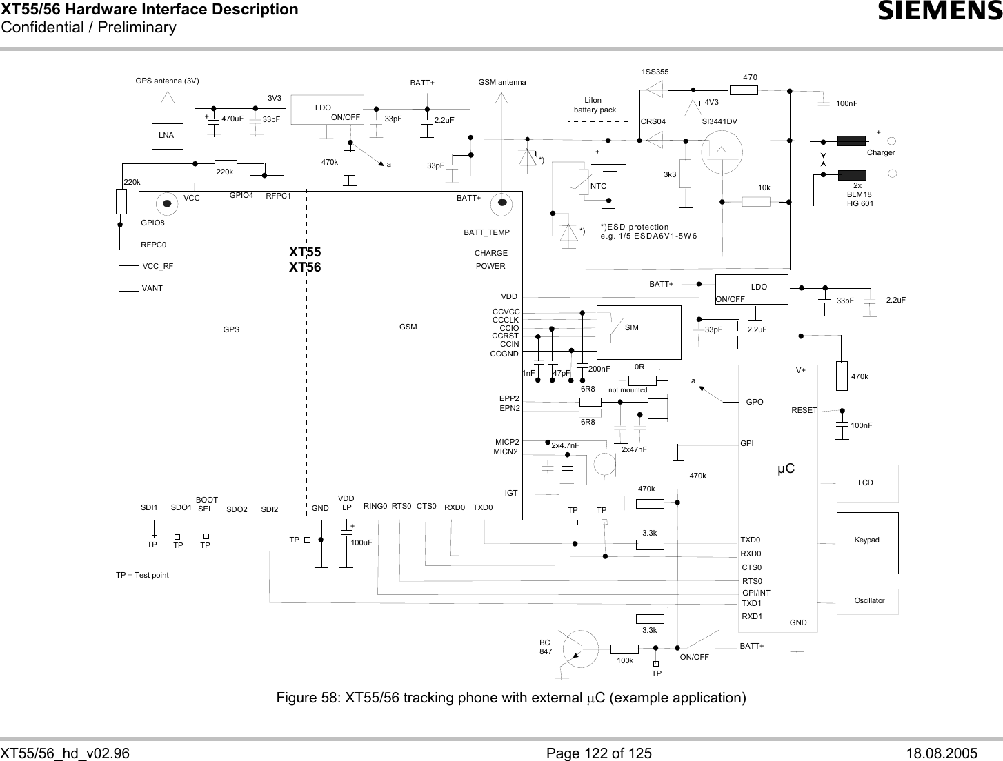
![XT55/56 Hardware Interface Description Confidential / Preliminary s XT55/56_hd_v02.96 Page 12 of 125 18.08.2005 1.2 Related Documents [1] XT55 AT Command Set XT56 AT Command Set [2] XT55/56 GPS Command Specification [3] XT55/56 Release Note [4] XT55 AVL Software User’s Guide [5] XT55/56 GPS Startup User's Guide [6] XT55/56 GSM/GPS Evaluation Board Description [7] GPRS Startup User's Guide [8] Remote-SAT User's Guide [9] DSB45 Support Box - Evaluation Kit for Siemens Cellular Engines [10] Application Note 14: Audio and Battery Parameter Download [11] Application Note 02: Audio Interface Design [12] Application Note 22: Using TTY / CTM equipment [13] Multiplexer User's Guide [14] Multiplex Driver Developer’s Guide for Windows 2000 and Windows XP [15] Multiplex Driver Installation Guide for Windows 2000 and Windows XP [16] Application Note 24: Application Developer’s Guide [17] Application Note 28: Customer SIM Lock [18] Application Note 21: Implementing Customer IMEI Prior to using the XT55/56 engines or upgrading to a new firmware release, be sure to carefully read the latest product information. To visit the Siemens Website you can use the following link: http://www.siemens.com/wm](https://usermanual.wiki/Telit-Cinterion-Deutschland/XT55.Updated-Usaer-Manual/User-Guide-585513-Page-12.png)
![XT55/56 Hardware Interface Description Confidential / Preliminary s XT55/56_hd_v02.96 Page 30 of 125 18.08.2005 3.2.2 Minimizing Power Losses When designing the power supply for your application please pay specific attention to power losses. Ensure that the input voltage VGSM_BATT+ never drops below 3.3V on the GSM part of the XT55/56 board, not even in a transmit burst where current consumption can rise to typical peaks of 1.6A. It should be noted that the GSM part of the XT55/56 module switches off when exceeding these limits. Any voltage drops that may occur in a transmit burst should not exceed 400mV. For further details see Chapter 6.4. The best approach to reducing voltage drops is to use a board-to-board connection as recommended, and a low impedance power source. The resistance of the power supply lines on the host board and of a battery pack should also be considered. Note: If the application design requires an adapter cable between both board-to-board connectors, use a cable as short as possible in order to minimize power losses. Example: If the length of the cable reaches the maximum length of 200mm, this connection may cause, for example, a resistance of 50m in the GSM_BATT+ line and 50m in the GND line. As a result, a 1.6A transmit burst would add up to a total voltage drop of 160mV. Plus, if a battery pack is involved, further losses may occur due to the resistance across the battery lines and the internal resistance of the battery including its protective circuit. Transmit burst 1.6ATransmit burst 1.6ARippleDropmin. 3.3VGSM_BATT+ Figure 3: Power supply limits during transmit burst The input voltage VGSM_BATT+ must be measured directly at the test points on the XT55/56 board (TP GSM_BATT+ and TP GND illustrated in Figure 50). 3.2.3 Monitoring Power Supply To help you monitor the supply voltage you can use the AT^SBV command which returns the voltage measured at TP GSM_BATT+ and GND. The voltage is continuously measured at intervals depending on the operating mode on the RF interface. The duration of measuring ranges from 0.5s in TALK/DATA mode up to 50s when the GSM part of the XT55/56 is in IDLE mode or Limited Service (deregistered). The displayed voltage (in mV) is averaged over the last measuring period before the AT^SBV command was executed. For details please refer to [1].](https://usermanual.wiki/Telit-Cinterion-Deutschland/XT55.Updated-Usaer-Manual/User-Guide-585513-Page-30.png)
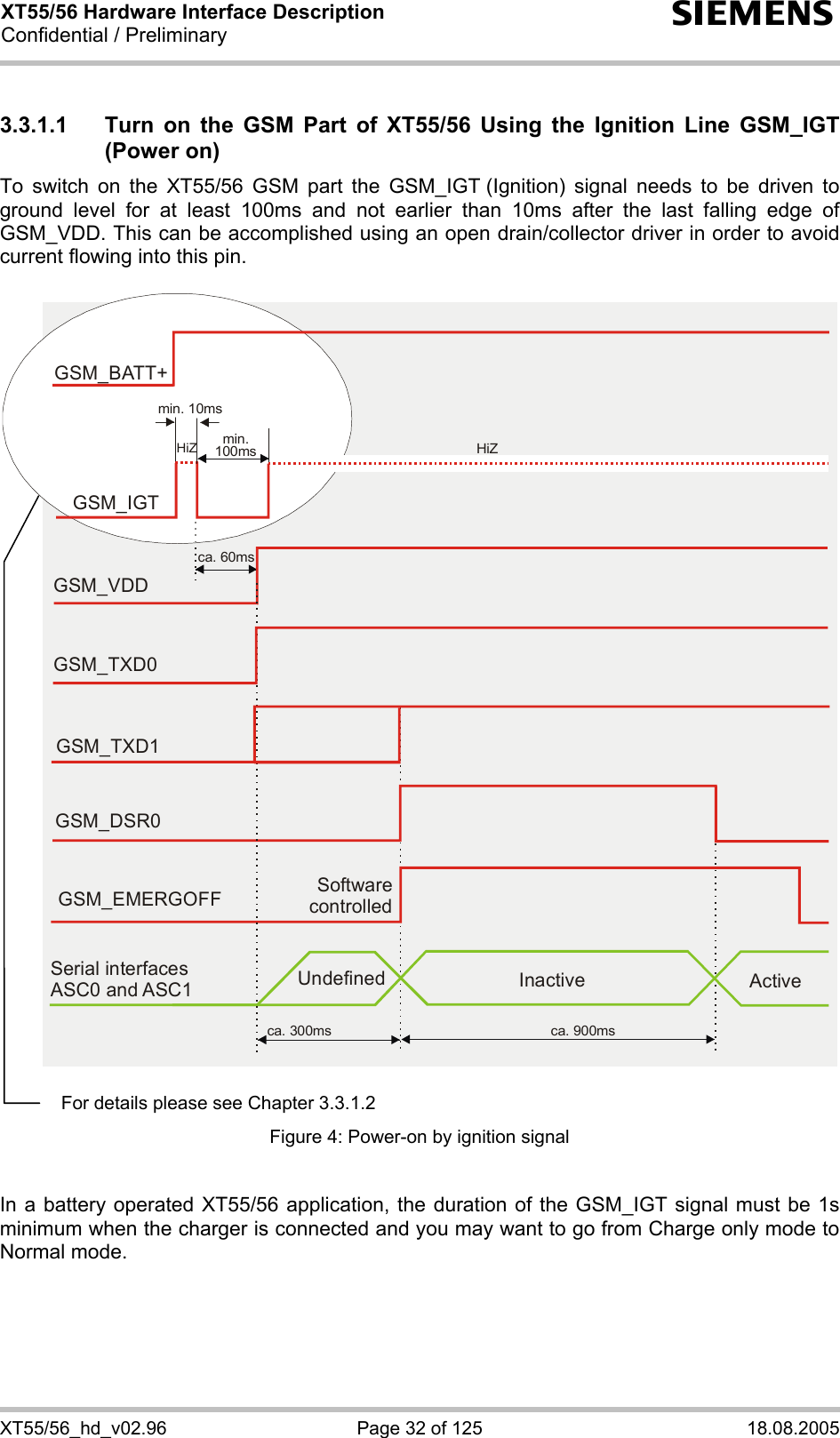
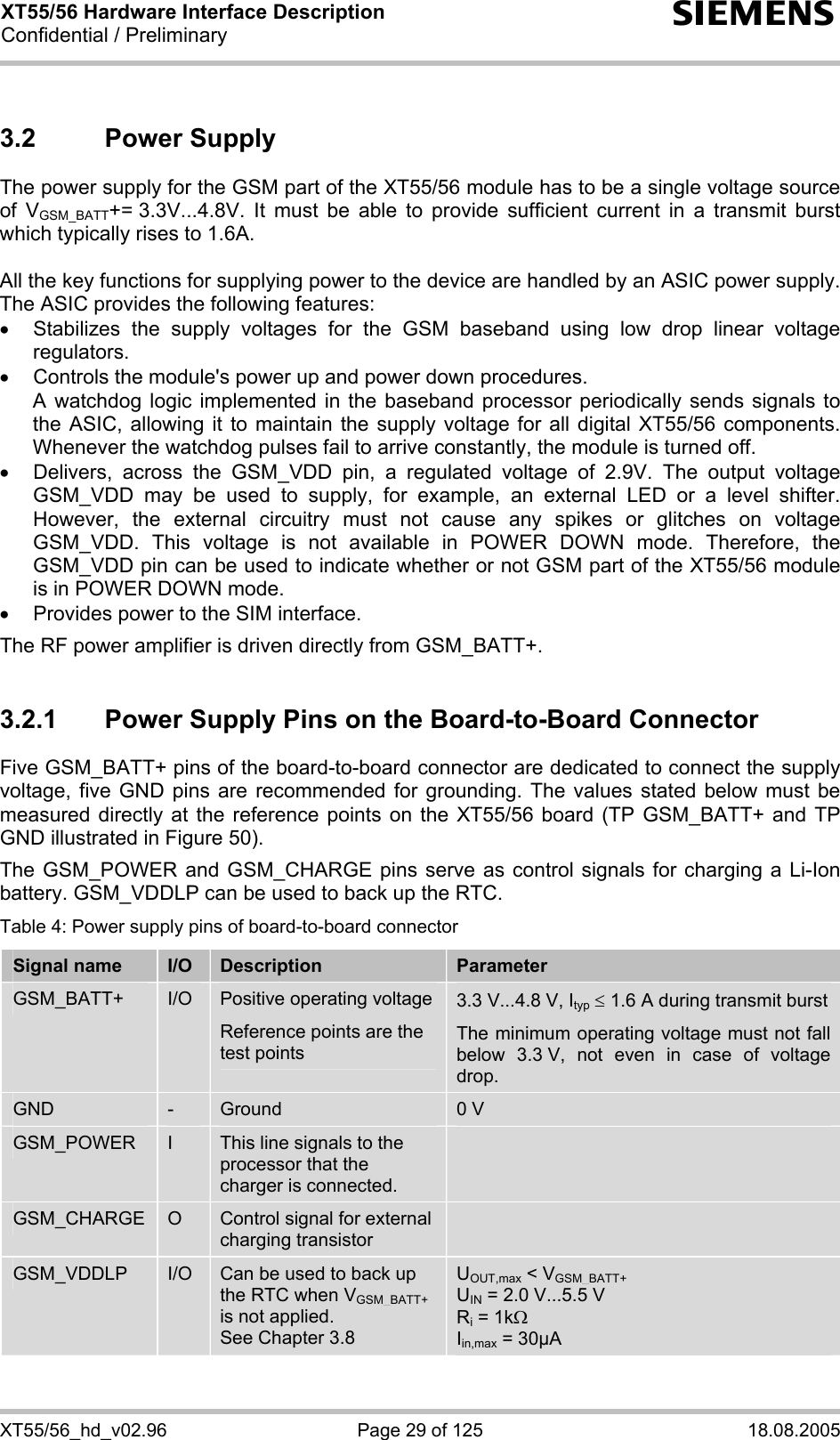
![XT55/56 Hardware Interface Description Confidential / Preliminary s XT55/56_hd_v02.96 Page 33 of 125 18.08.2005 Assertion of GSM_CTS indicates that the module is ready to receive data from the host application. In addition, if configured to a fixed bit rate (AT+IPR0), the module will send the URC “^SYSSTART” which notifies the host application that the first AT command can be sent to the module. The duration until this URC is output varies with the SIM card and may take a couple of seconds, particularly if the request for the SIM PIN is deactivated on the SIM card. Please note that no “^SYSSTART” URC will be generated if autobauding (AT+IPR=0) is enabled. To allow the application to detect the ready state of the module we recommend using hardware flow control which can be set with AT\Q or AT+ICF (see [1] for details). The default setting of XT55/56 is AT\Q0 (no flow control) which shall be altered to AT\Q3 (RTS/CTS handshake). If the application design does not integrate RTS/CTS lines the host application shall wait at least for the “^SYSSTART” URC. However, if the URCs are neither used (due to autobauding) then the only way of checking the module’s ready state is polling. To do so, try to send characters (e.g. “at”) until the module is responding. 3.3.1.2 Timing of the Ignition Process When designing your application platform take into account that powering up the GSM part of the XT55/56 module requires the following steps. • The ignition line cannot be operated until VGSM_BATT+ passes the level of 3.0V. • The ignition line shall not be operated earlier than 10ms after the last falling edge of GSM_VDD. • 10ms after VGSM_BATT+ has reached 3.0V the ignition line can be switched low. The duration of the falling edge must not exceed 1ms. • Another 100ms are required to power up the module. • Ensure that VGSM_BATT+ does not fall below 3.0V while the ignition line is driven. Otherwise the module cannot be activated. • If the GSM_VDDLP line is fed from an external power supply as explained in Chapter 3.8, the GSM_IGT line is HiZ before the rising edge of GSM_BATT+. Figure 5: Timing of power-on process if GSM_VDDLP is not used 3.0V0VGSM_BATT+min. 100msmax. 1ms10msGSM_IGTHiZHiZ](https://usermanual.wiki/Telit-Cinterion-Deutschland/XT55.Updated-Usaer-Manual/User-Guide-585513-Page-33.png)
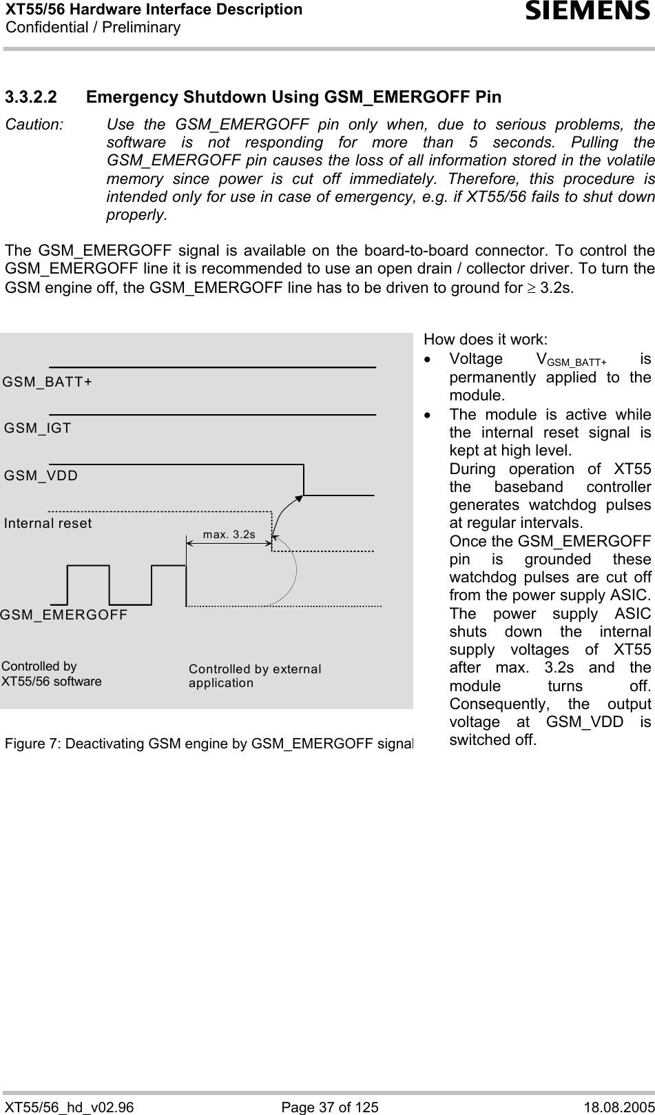
![XT55/56 Hardware Interface Description Confidential / Preliminary s XT55/56_hd_v02.96 Page 38 of 125 18.08.2005 3.3.3 Automatic Shutdown Automatic shutdown takes effect if • the XT55/56 board is exceeding the critical limits of overtemperature or undertemperature • the battery is exceeding the critical limits of overtemperature or undertemperature • undervoltage is detected The automatic shutdown procedure is equivalent to the power-down initiated with the AT^SMSO command, i.e. XT55/56 logs off from the network and the software enters a secure state avoiding loss of data. NOTE: This does not apply if overvoltage conditions or unrecoverable hardware or software errors occur (see below for details). Alert messages transmitted before the device switches off are implemented as Unsolicited Result Codes (URCs). The presentation of these URCs can be enabled or disabled with the two AT commands AT^SBC and AT^SCTM. The URC presentation mode varies with the condition, please see Chapters 3.3.3.1 to 3.3.3.4 for details. For further instructions on AT commands refer to [1]. 3.3.3.1 Temperature Dependent Shutdown The board temperature is constantly monitored by an internal NTC resistor located on the PCB. The NTC that detects the battery temperature must be part of the battery pack circuit as described in Chapter 3.5. The values detected by either NTC resistor are measured directly on the board or the battery and therefore, are not fully identical with the ambient temperature. Each time the board or battery temperature goes out of range or back to normal, XT55/56 instantly displays an alert (if enabled). • URCs indicating the level "1" or "-1" allow the user to take appropriate precautions, such as protecting the module from exposure to extreme conditions. The presentation of the URCs depends on the settings selected with the AT^SCTM write command: AT^SCTM=1: Presentation of URCs is always enabled. AT^SCTM=0 (default): Presentation of URCs is enabled for 15 seconds time after start-up of XT55/56. After 15 seconds operation, the presentation will be disabled, i.e. no alert messages can be generated. • URCs indicating the level "2" or "-2" are instantly followed by an orderly shutdown. The presentation of these URCs is always enabled, i.e. they will be output even though the factory setting AT^SCTM=0 was never changed. The maximum temperature ratings are stated in Table 26. Refer to Table 6 for the associated URCs. All statements are based on test conditions according to IEC 60068-2-2 (still air).](https://usermanual.wiki/Telit-Cinterion-Deutschland/XT55.Updated-Usaer-Manual/User-Guide-585513-Page-38.png)
![XT55/56 Hardware Interface Description Confidential / Preliminary s XT55/56_hd_v02.96 Page 39 of 125 18.08.2005 Table 6: Temperature dependent behavior Sending temperature alert (15 s after start-up, otherwise only if URC presentation enabled) ^SCTM_A: 1 Caution: Tamb of battery close to over temperature limit. ^SCTM_B: 1 Caution: Tamb of board close to over temperature limit. ^SCTM_A: -1 Caution: Tamb of battery close to under temperature limit. ^SCTM_B: -1 Caution: Tamb of board close to under temperature limit. ^SCTM_A: 0 Battery back to uncritical temperature range. ^SCTM_B: 0 Board back to uncritical temperature range. Automatic shutdown (URC appears no matter whether or not presentation was enabled) ^SCTM_A: 2 Alert: Tamb of battery equal or beyond over temperature limit. XT55/56 switches off. ^SCTM_B: 2 Alert: Tamb of board equal or beyond over temperature limit. XT55/56 switches off. ^SCTM_A: -2 Alert: Tamb of battery equal or below under temperature limit. XT55/56 switches off. ^SCTM_B: -2 Alert: Tamb of board equal or below under temperature limit. XT55/56 switches off. 3.3.3.2 Temperature Control during Emergency Call If the temperature limit is exceeded while an emergency call is in progress the engine continues to measure the temperature, but deactivates the shutdown functionality. If the temperature is still out of range when the call ends, the module switches off immediately (without another alert message). 3.3.3.3 Undervoltage Shutdown if Battery NTC is Present In applications where the module’s charging technique is used and an NTC is connected to the GSM_BATT_TEMP terminal, the software constantly monitors the applied voltage. If the measured battery voltage is no more sufficient to set up a call the following URC will be presented: ^SBC: Undervoltage. The message will be reported, for example, when you attempt to make a call while the voltage is close to the critical limit and further power loss is caused during the transmit burst. To remind you that the battery needs to be charged soon, the URC appears several times before the module switches off. To enable or disable the URC use the AT^SBC command. The URC will be enabled when you enter the write command and specify the power consumption of your GSM application. Step by step instructions are provided in [1].](https://usermanual.wiki/Telit-Cinterion-Deutschland/XT55.Updated-Usaer-Manual/User-Guide-585513-Page-39.png)
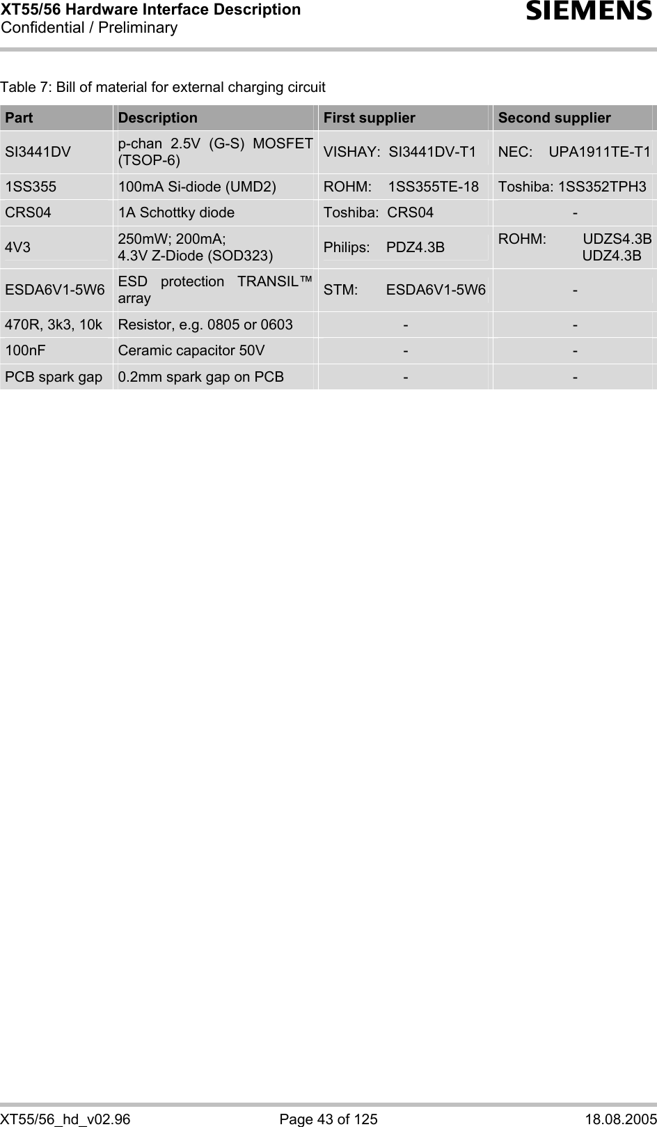
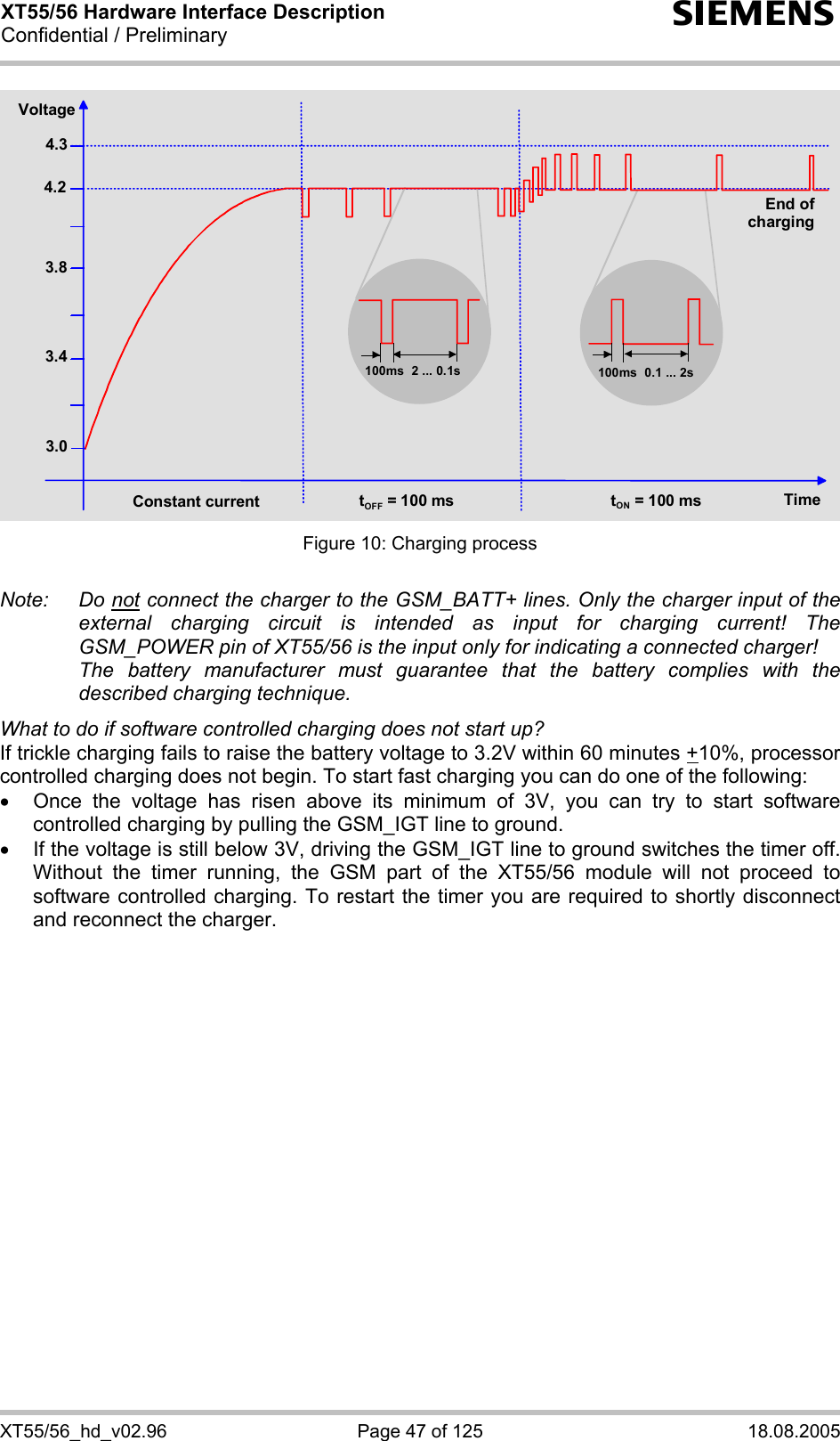
![XT55/56 Hardware Interface Description Confidential / Preliminary s XT55/56_hd_v02.96 Page 42 of 125 18.08.2005 3.5 Charging Control of the GSM Part The GSM part of the XT55/56 module integrates a charging management for Li-Ion batteries. You can skip this chapter if charging is not your concern, or if you are not using the implemented charging algorithm. XT55/56 has no on-board charging circuit. To benefit from the implemented charging management you are required to install a charging circuit within your application. In this case, XT55/56 needs to be powered from a Li-Ion battery pack, e.g. as specified in Table 8. Note: The charging control described in this chapter is integrated in the GSM part of the XT55/56 and has been optimized for it only. When using the charging control function for the entire XT55/56 module, please consider the current consumption of the GPS part and your application. The value can be set with the AT^SBC command. This command should be used to specify the power consumption if the GSM part, the GPS part and your application are powered from the same battery. For further details refer to [1]. For using the trickle charging functionality you should design the 470R (illustrated in Figure 8) according to the current consumption of your application. The module only delivers, via its GSM_POWER line and GSM_CHARGE line, the control signals needed to start and stop the charging process. The charging circuit should include a transistor and should be designed as illustrated in Figure 8. A list of parts recommended for the external circuit is given in Table 7. to GSM_BATT+Input fromcharger(5.5V - 8V)under loadGSM_CHARGE470R 1SS3553k3100nF 10kSI3441DV4V31/ 5 ESDA6V1-5W6to GSM_POWERGSM_BATT_TEMP1/ 5 ESDA6V1-5W6NTC+Battery packPCB spark gapCRS04- Figure 8: Schematic of approved charging transistor, trickle charging and ESD protection](https://usermanual.wiki/Telit-Cinterion-Deutschland/XT55.Updated-Usaer-Manual/User-Guide-585513-Page-42.png)
![XT55/56 Hardware Interface Description Confidential / Preliminary s XT55/56_hd_v02.96 Page 44 of 125 18.08.2005 3.5.1 Battery Pack Characteristics The charging algorithm has been optimized for a Li-Ion battery pack that meets the characteristics listed below. It is recommended that the battery pack you want to integrate into your XT55/56 application is compliant with these specifications. This ensures reliable operation, proper charging and, particularly, allows you to monitor the battery capacity using the AT^SBC command (see [1] for details). Failure to comply with these specifications might cause AT^SBC to deliver incorrect battery capacity values. A battery pack especially designed to operate with XT55/56 modules is specified in Chapter 3.5.2. • Li-Ion battery pack specified for a maximum charging voltage of 4.2 V and a capacity of 800 mAh. Battery packs with a capacity down to 600 mAh or more than 800 mAh are allowed, too. • Since charging and discharging largely depend on the battery temperature, the battery pack should include an NTC resistor. If the NTC is not inside the battery it must be in thermal contact with the battery. The NTC resistor must be connected between GSM_BATT_TEMP and GND. Required NTC characteristics are: 10 kΩ +5% @ 25°C, B25/85 = 3435K +3% (alternatively acceptable: 10 kΩ +2% @ 25°C, B25/50 = 3370K +3%). Please note that the NTC is indispensable for proper charging, i.e. the charging process will not start if no NTC is present. • Ensure that the pack incorporates a protection circuit capable of detecting overvoltage (protection against overcharging), undervoltage (protection against deep discharging) and overcurrent. The circuit must be insensitive to pulsed current. • On the XT55/56 module, a built-in measuring circuit constantly monitors the supply voltage. In the event of undervoltage, it causes XT55/56 to power down. Undervoltage thresholds are specific to the battery pack and must be evaluated for the intended model. When you evaluate undervoltage thresholds, consider both the current consumption of XT55/56 and of the application circuit. • The internal resistance of the battery and the protection should be as low as possible. It is recommended not to exceed 150m, even in extreme conditions at low temperature. The battery cell must be insensitive to rupture, fire and gassing under extreme conditions of temperature and charging (voltage, current). • The battery pack must be protected from reverse pole connection. For example, the casing should be designed to prevent the user from mounting the battery in reverse orientation. • The battery pack must be approved to satisfy the requirements of CE conformity. Figure 9 shows the circuit diagram of a typical battery pack design that includes the protection elements described above. Figure 9: Battery pack circuit diagram to GSM_BATT_TEMP to GNDNTCPolyfuseϑProtection Circuit+-Battery cellto GSM_BATT+](https://usermanual.wiki/Telit-Cinterion-Deutschland/XT55.Updated-Usaer-Manual/User-Guide-585513-Page-44.png)
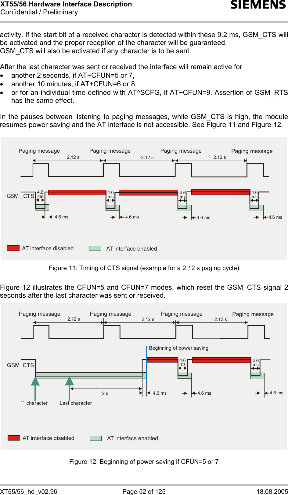
![XT55/56 Hardware Interface Description Confidential / Preliminary s XT55/56_hd_v02.96 Page 50 of 125 18.08.2005 3.6 Power Saving SLEEP mode reduces the functionality of the GSM part of the XT55/56 module to a minimum and, thus, minimizes the current consumption to the lowest level. Settings can be made using the AT+CFUN command. For details see below and [1]. SLEEP mode falls into two categories: • NON-CYCLIC SLEEP mode AT+CFUN=0 • CYCLIC SLEEP modes, selectable with AT+CFUN=5, 6, 7, 8 or 9. IMPORTANT: Please keep in mind that power saving works properly only when PIN authentication has been done. If you attempt to activate power saving while the SIM card is not inserted or the PIN not correctly entered (Limited Service), the selected <fun> level will be set, though power saving does not take effect. For the same reason, power saving cannot be used if the GSM part of the XT55/56 operates in Alarm mode. To check whether power saving is on, you can query the status of AT+CFUN if you have chosen CYCLIC SLEEP mode. If available, you can take advantage of the status LED controlled by the GSM_SYNC pin (see Chapter 3.12.2.2). The LED is off in all SLEEP modes when no activity occurs, but resumes flashing to indicate temporary wake-up states during CYLCIC SLEEP modes. The LED patterns are shown in Table 18. The wake-up procedures are quite different depending on the selected SLEEP mode. Table 11 compares the wake-up events that can occur in NON-CYCLIC and CYCLIC SLEEP modes. 3.6.1 No Power Saving (AT+CFUN=1) The functionality level <fun>=1 is where power saving is switched off. This is the default after startup. 3.6.2 NON-CYCLIC SLEEP Mode (AT+CFUN=0) If level 0 has been selected (AT+CFUN=0), the serial interface is blocked. The module shortly deactivates power saving to listen to a paging message sent from the base station and then immediately resumes power saving. Level 0 is called NON-CYCLIC SLEEP mode, since the serial interface is not alternatingly made accessible as in CYCLIC SLEEP mode. The first wake-up event fully activates the module, enables the serial interface and terminates the power saving mode. In short, it takes the GSM part of the XT55/56 back to the highest level of functionality <fun>=1. In NON-CYCLIC mode, the falling edge of the GSM_RTS0 or GSM_RTS1 lines wakes up the module to <fun>=1. To efficiently use this feature it is recommended to enable hardware flow control (RTS/CTS handshake) as in this case the GSM_CTS line notifies the application when the module is ready to send or receive characters. See section 3.6.5.1 for details.](https://usermanual.wiki/Telit-Cinterion-Deutschland/XT55.Updated-Usaer-Manual/User-Guide-585513-Page-50.png)
![XT55/56 Hardware Interface Description Confidential / Preliminary s XT55/56_hd_v02.96 Page 51 of 125 18.08.2005 3.6.3 CYCLIC SLEEP Mode (AT+CFUN=5, 6, 7, 8) The major benefit over the NON-CYCLIC SLEEP mode is that the serial interface is not permanently blocked and that packet switched calls may go on without terminating the selected CYCLIC SLEEP mode. This allows the GSM part of the XT55/56 to become active, for example to perform a GPRS data transfer, and to resume power saving after the GPRS data transfer is completed. The CYCLIC SLEEP modes give you greater flexibility regarding the wake-up procedures: For example, in all CYCLIC SLEEP modes, you can enter AT+CFUN=1 to permanently wake up the module. In modes CFUN=7 and 8, the GSM part of the XT55/56 automatically resumes power saving, after you have sent or received a short message or made a call. CFUN=5 and 6 do not offer this feature, and therefore, are only supported for compatibility with earlier releases. Please refer to Table 11 for a summary of all modes. The CYCLIC SLEEP mode is a dynamic process which alternatingly enables and disables the serial interface. By setting/resetting the GSM_CTS signal, the module indicates to the application whether or not the UART is active. The timing of GSM_CTS is described below. Both the application and the module must be configured to use hardware flow control (RTS/CTS handshake). The default setting of the GSM part of the XT55/56 is AT\Q0 (no flow control) which must be altered to AT\Q3. See [1] for details. Note: If both serial interfaces ASC0 and ASC1 are connected, both are synchronized. This means that SLEEP mode takes effect on both, no matter on which interface the AT command was issued. Although not explicitly stated, all explanations given in this chapter refer equally to ASC0 and ASC1, and accordingly to GSM_CTS0 and GSM_CTS1. 3.6.4 CYCLIC SLEEP Mode AT+CFUN=9 Mode AT+CFUN=9 is similar to AT+CFUN=7 or 8, but provides two additional features: • The time the module stays active after GSM_RTS was asserted or after the last character was sent or received, can be configured individually using the command AT^SCFG. Default setting is 2 seconds like in AT+CFUN=7. The entire range is from 0.5 seconds to 1 hour, selectable in tenths of seconds. For details see [1]. • GSM_RTS0 and GSM_RTS1 are not only used for flow control (as in modes AT+CFUN=5, 6, 7 or 8), but also cause the module to wake up temporarily. See section 3.6.5.1 for details. 3.6.5 Timing of the GSM_CTS Signal in CYCLIC SLEEP Modes The GSM_CTS signal is enabled in synchrony with the module’s paging cycle. It goes active low each time when the module starts listening to a paging message block from the base station. The timing of the paging cycle varies with the base station. The duration of a paging interval can be calculated from the following formula: 4.615 ms (TDMA frame duration) * 51 (number of frames) * DRX value. DRX (Discontinuous Reception) is a value from 2 to 9, resulting in paging intervals from 0.47 to 2.12 seconds. The DRX value of the base station is assigned by the network operator. Each listening period causes the GSM_CTS signal to go active low: If DRX is 2, the GSM_CTS signal is activated every 0.47 seconds, if DRX is 3, the GSM_CTS signal is activated every 0.71 seconds and if DRX is 9, the GSM_CTS signal is activated every 2.1s. The GSM_CTS signal is active low for 4.6 ms. This is followed by another 4.6 ms UART](https://usermanual.wiki/Telit-Cinterion-Deutschland/XT55.Updated-Usaer-Manual/User-Guide-585513-Page-51.png)
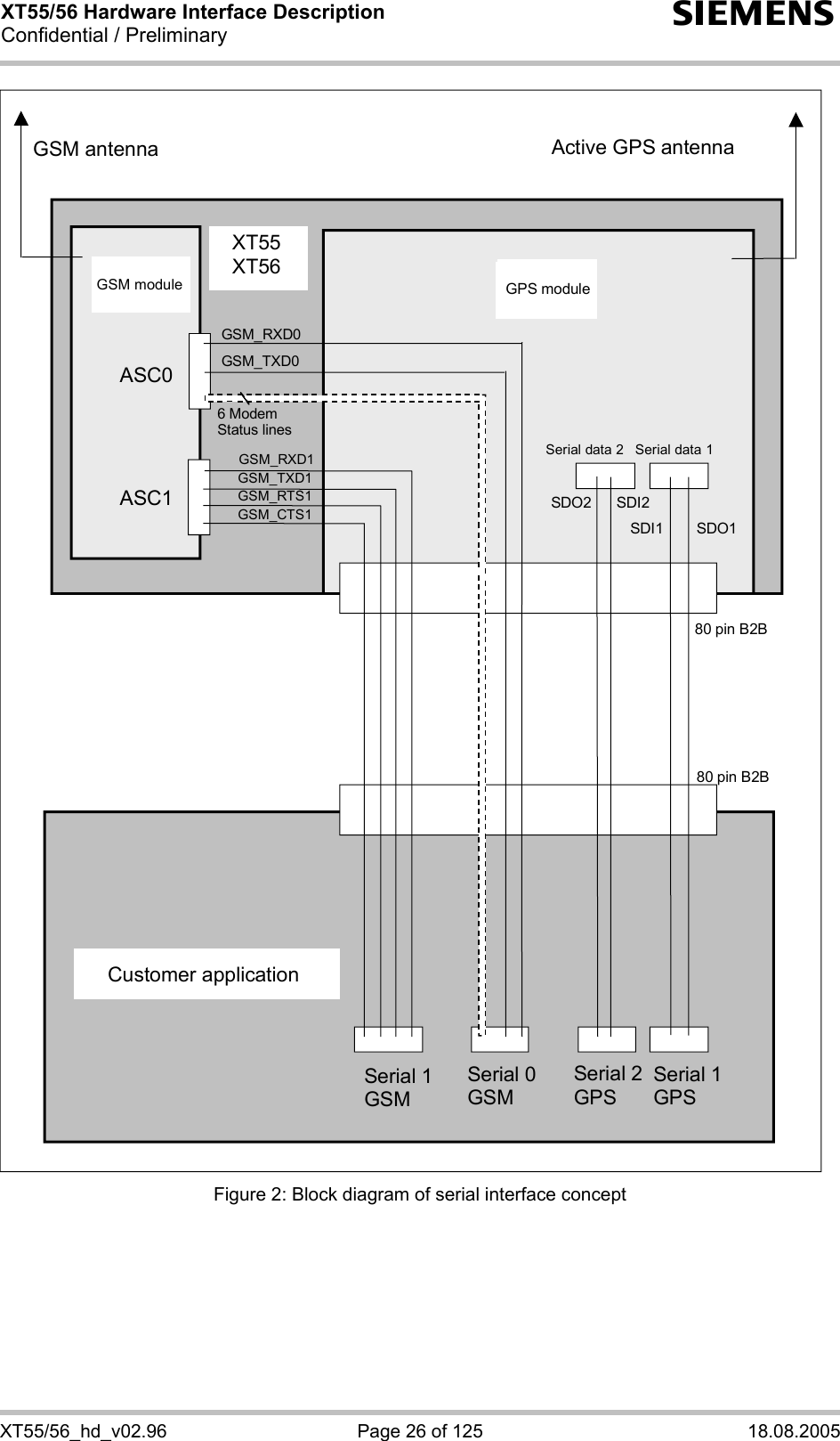
![XT55/56 Hardware Interface Description Confidential / Preliminary s XT55/56_hd_v02.96 Page 57 of 125 18.08.2005 3.9 Serial Interfaces of the XT55/56 GSM Part The GSM part of the XT55/56 module offers two unbalanced, asynchronous serial interfaces conforming to ITU-T V.24 protocol DCE signaling. The electrical characteristics do not comply with ITU-T V.28. The significant levels are 0V (for low data bit or ON condition) and 2.65V (for high data bit or OFF condition). For electrical characteristics please refer to Table 38. Figure 2 shows the serial interfaces of the XT55/56 module. The GSM engine is designed for use as a DCE. Based on the conventions for DCE-DTE connections it communicates with the customer application (DTE) using the following signals: ASC0 • Port TXD @ application sends data to the module’s GSM_TXD0 signal line • Port RXD @ application receives data from the module’s GSM_RXD0 signal line ASC1 • Port TXD @ application sends data to module’s GSM_TXD1 signal line • Port RXD @ application receives data from the module’s GSM_RXD1 signal line 3.9.1 Features of the first Serial Interface of the GSM Part (ASC0) • 8-wire serial interface • Includes the data lines GSM_TXD0 and GSM_RXD0, the status lines GSM_RTS0 and GSM_CTS0 and, in addition, the modem control lines GSM_DTR0, GSM_DSR0, GSM_DCD0 and GSM_RING0. • It is primarily designed for voice calls, CSD calls, fax calls and GPRS services and for controlling the GSM engine with AT commands. Full Multiplex capability allows the interface to be partitioned into three virtual channels, yet with CSD and fax services only available on the first logical channel. Please note that when the ASC0 interface runs in Multiplex mode, ASC1 cannot be used. For more detailed characteristics see [13]. • The GSM_DTR0 signal will only be polled once per second from the internal firmware of XT55/56. • The GSM_RING0 signal serves to indicate incoming calls and other types of URCs (Unsolicited Result Code). It can also be used to send pulses to the host application, for example to wake up the application from power saving state. For further details see Chapter 3.12.3. • Autobauding is only selectable on ASC0 and supports the following bit rates: 1200, 2400, 4800, 9600, 19200, 38400, 57600, 115200, 230400 bps. • Autobauding is not compatible with multiplex mode, see [13]. • ASC0 interface is intended for firmware upgrade of the GSM part](https://usermanual.wiki/Telit-Cinterion-Deutschland/XT55.Updated-Usaer-Manual/User-Guide-585513-Page-57.png)
![XT55/56 Hardware Interface Description Confidential / Preliminary s XT55/56_hd_v02.96 Page 58 of 125 18.08.2005 3.9.2 Features of the second Serial Interface of GSM Part (ASC1) • 4-wire serial interface • Includes only the data lines GSM_TXD1 and GSM_RXD1 plus GSM_RTS1 and GSM_CTS1 for hardware handshake. This interface is intended for voice calls, GPRS services and for controlling the GSM engine with AT commands. It is not suited for CSD calls, fax calls and Multiplex mode. • On ASC1 no GSM_RING line is available. The indication of URCs on the second interface depends on the settings made with the AT^SCFG command. For details refer to [1]. 3.9.3 ASC0 and ASC1 Configuration • Both interfaces are configured for 8 data bits, no parity and 1 stop bit, and can be operated at bit rates from 300bps to 230400 bps. • XON/XOFF software flow control can be used on both interfaces (except if power saving is active). Table 13: DCE-DTE wiring of 1st serial interface (GSM part) DCE (XT55/56) DTE (application) V.24 circuit Pin function Signal direction Pin function Signal direction 103 GSM_TXD0 Input /TXD Output 104 GSM_RXD0 Output /RXD Input 105 GSM_RTS0 Input /RTS Output 106 GSM_CTS0 Output /CTS Input 108/2 GSM_DTR0 Input /DTR Output 107 GSM_DSR0 Output /DSR Input 109 GSM_DCD0 Output /DCD Input 125 GSM_RING0 Output /RING Input Table 14: DCE-DTE wiring of 2nd serial interface (GSM part) DCE (XT55/56) DTE (application) V.24 circuit Pin function Signal direction Pin function Signal direction 103 GSM_TXD1 Input /TXD Output 104 GSM_RXD1 Output /RXD Input 105 GSM_RTS1 Input /RTS Output 106 GSM_CTS1 Output /CTS Input](https://usermanual.wiki/Telit-Cinterion-Deutschland/XT55.Updated-Usaer-Manual/User-Guide-585513-Page-58.png)
![XT55/56 Hardware Interface Description Confidential / Preliminary s XT55/56_hd_v02.96 Page 59 of 125 18.08.2005 3.10 Audio Interfaces XT55/56 comprises three audio interfaces available on the board-to-board connector: • Two analog audio interfaces, each with a balanced analog microphone input and a balanced analog earpiece output. The second analog interface provides a supply circuit to feed an active microphone. • Serial digital audio interface (DAI) using PCM (Pulse Code Modulation) to encode analog voice signals into digital bit streams. This means you can connect up to three audio devices in any combination, although analog and digital audio cannot be operated at the same time. Using the AT^SAIC command you can easily switch back and forth. M U X ADC DSP DAC Air InterfaceDigital Audio Interface (DAI) GSM_MICP1 GSM_MICN1 GSM_MICP2 GSM_MICN2 GSM_EPP1 GSM_EPN1 GSM_EPP2 GSM_EPN2 GSM_SCLK GSM_RXDDAI GSM_TFSDAI GSM_RFSDAI GSM_TXDDAI Figure 16: Audio block diagram XT55/56 offers six audio modes which can be selected with the AT^SNFS command, no matter which of the three interfaces is currently active. The electrical characteristics of the voiceband part vary with the audio mode. For example, sending and receiving amplification, sidetone paths, noise suppression etc. depend on the selected mode and can be altered with AT commands (except for mode 1). On each audio interface you can use all audio AT commands specified in [1] to alter parameters. The only exception are the DAC and ADC gain amplifier attenuation <outBbcGain> and <inBbcGain> which cannot be modified when the digital audio interface is used, since in this case the DAC and ADC are switched off. Please refer to Chapter 3.10 for specifications of the audio interface and an overview of the audio parameters. Detailed instructions on using AT commands are presented in [1]. Table 31 on page 105 summarizes the characteristics of the various audio modes and shows what parameters are supported in each mode.](https://usermanual.wiki/Telit-Cinterion-Deutschland/XT55.Updated-Usaer-Manual/User-Guide-585513-Page-59.png)
![XT55/56 Hardware Interface Description Confidential / Preliminary s XT55/56_hd_v02.96 Page 60 of 125 18.08.2005 When shipped from factory, all audio parameters of XT55/56 are set to interface 1 and audio mode 1. This is the default configuration optimized for the Votronic HH-SI-30.3/V1.1/0 handset and used for type approving the Siemens reference configuration. Audio mode 1 has fix parameters which cannot be modified. To adjust the settings of the Votronic handset simply change to another audio mode. In transmit direction, all audio modes contain internal scaling factors (digital amplification) that are not accessible by the user. To avoid saturation with a full scale digital input signal on the DAI, and to obtain a one-to-one digital access to the speech coder in audio mode 5 and 6, it is recommended to set the parameter <inCalibrate> of the selected audio mode as follows: Audio mode 1 and 4: 23196 Audio mode 2: 17396 Audio mode 3: 21901 Audio mode 5 and 6: 21402 3.10.1 Microphone Circuit Interface 1 This interface has no microphone supply circuit and therefore, has an impedance of 50kΩ. When connecting a microphone or another signal source to interface 1 you are required to add two 100 nF capacitors, one to each line. Interface 2 This interface comes with a microphone supply circuit and can be used to feed an active microphone. It has an impedance of 2kΩ. If you do not use it or if you want to connect another type of signal source, for example, an op amp or a dynamic microphone, it needs to be decoupled with capacitors. The power supply can be switched off and on by using the command AT^SNFM. For details see [1]. Figure 17 shows the microphone inputs at both analog interfaces of XT55/56. 2.65 V to ADC Power down GSM_MICP1 GSM_MICN1 GSM_MICP2 GSM_MICN2 1 k 1 k 1 k 1 k33 µF Ri=50k Ri=2k Figure 17: Schematic of microphone inputs](https://usermanual.wiki/Telit-Cinterion-Deutschland/XT55.Updated-Usaer-Manual/User-Guide-585513-Page-60.png)
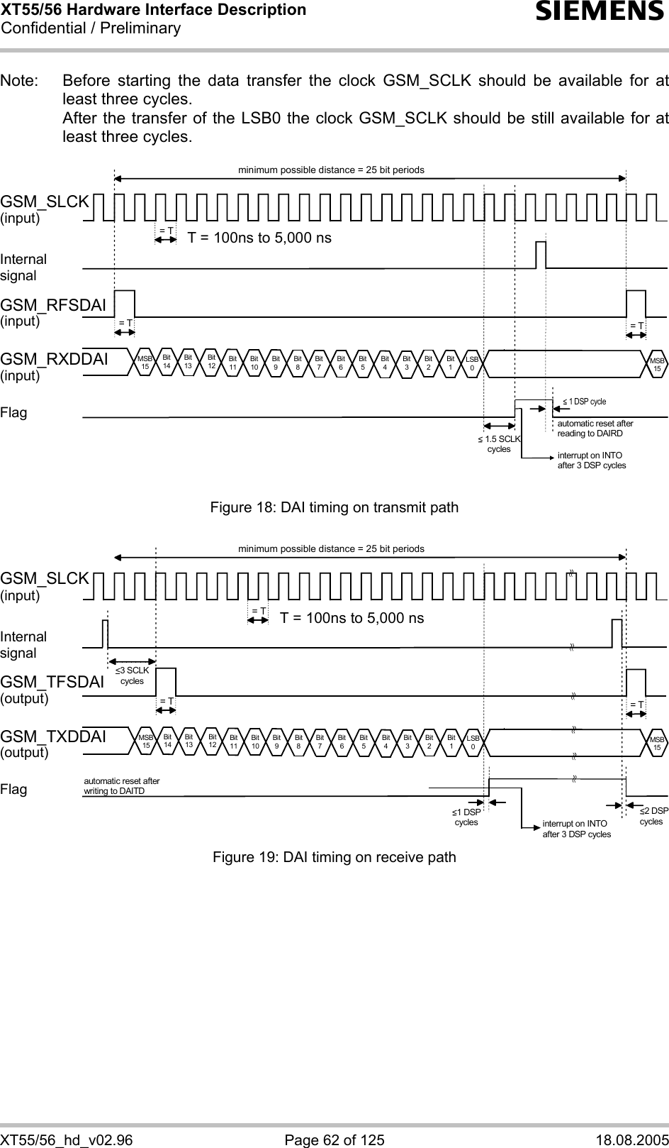
![XT55/56 Hardware Interface Description Confidential / Preliminary s XT55/56_hd_v02.96 Page 61 of 125 18.08.2005 3.10.2 Speech Processing The speech samples from the ADC or DAI are handled by the DSP of the baseband controller to calculate e.g. amplifications, sidetone, echo cancellation or noise suppression depending on the configuration of the active audio mode. These processed samples are passed to the speech encoder. Received samples from the speech decoder are passed to the DAC or DAI after post processing (frequency response correction, adding sidetone etc.). Full rate, half rate, enhanced full rate, adaptive multi rate (AMR), speech and channel encoding including voice activity detection (VAD) and discontinuous transmission (DTX) and digital GMSK modulation are also performed on the GSM baseband processor. Customer specific audio parameters can be evaluated and supplied by Siemens on request. These parameters can be downloaded to XT55/56 using an AT command. For further information refer to [10] or contact your Siemens distributor. 3.10.3 DAI Timing To support the DAI function, XT55/56 integrates a simple five-line serial interface with one input data clock line (GSM_SCLK) and input / output data and frame lines (GSM_TXDDAI, GSM_TFSDAI, GSM_RXDDAI, GSM_RFSDAI). The serial interface is always active if the external input data clock GSM_SLCK is present, i.e. the serial interface is not clocked by the DSP of the XT55/56 baseband processor. GSM_SLCK must be supplied from the application and can be in a frequency range between 0.2 and 10 MHz. Serial transfer of 16-bit words is done in both directions. Data transfer to the application is initiated by the module via a short pulse of GSM_TFSDAI. The duration of the GSM_TFSDAI pulse is one GSM_SCLK period, starting at the rising edge of SLCK. During the following 16 SLCK cycles, the 16-bit sample will be transferred on the GSM_TXDDAI line. The next outgoing sample will be transferred after the next GSM_TFSDAI pulse which occurs every 125 µs. The GSM_TFSDAI pulse is the master clock of the sample transfer. From the rising edge of the GSM_TFSDAI pulse, the application has 100 µs to transfer the 16-bit input sample on the GSM_RXDDAI line. The rising edge of the GSM_RFSDAI pulse (supplied by the application) may coincide with the falling edge of GSM_TFSDAI or occur slightly later - it is only significant that, in any case, the transfer of the LSB input sample will be completed within the specified duration of 100 µs. Audio samples are transferred from the module to the application in an average of 125µs. This is determined by the 8kHz sampling rate, which is derived from and synchronized to the GSM network. As SLCK is independent of the GSM network, the distance between two succeeding sample transfers may vary about + 1 SLCK period. The application is required to adapt its sampling rate to the GSM_TFSDAI rate. Failure to synchronize the timing between the module and the application may cause audible pops and clicks in a conversation. The timing characteristics of both data transfer directions are shown in Figure 18 and Figure 19.](https://usermanual.wiki/Telit-Cinterion-Deutschland/XT55.Updated-Usaer-Manual/User-Guide-585513-Page-61.png)
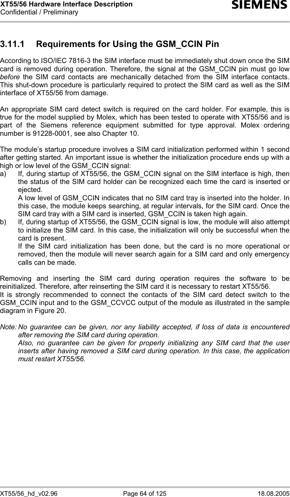
![XT55/56 Hardware Interface Description Confidential / Preliminary s XT55/56_hd_v02.96 Page 65 of 125 18.08.2005 3.11.2 Design Considerations for SIM Card Holder The schematic below is a sample configuration that illustrates the Molex SIM card holder located on the DSB45 Support Box (evaluation kit used for type approval of the Siemens XT55/56 reference setup, see [9]). X503 is the designation used for the SIM card holder in [9]. Molex card holder GSM moduleGSM_CCVCCGSM_CCINGSM_CCIOGSM_CCCLKGSM_CCRSTGSM_CCGND47pF Figure 20: SIM card holder of DSB45 Support Box Table 16: Pin assignment of Molex SIM card holder on DSB45 Support Box Pin no. Signal name I/O Function 1 CCVCC I Supply voltage for SIM card, generated by the GSM engine 2 CCRST I Chip card reset, prompted by the GSM engine 3 CCCLK I Chip card clock 4 CCGND - Individual ground line for the SIM card to improve EMC 5 CCVPP - Not connected 6 CCIO I/O Serial data line, bi-directional 7 CCDET1 - Connect to GSM_CCVCC 8 CCDET2 Connects to the GSM_CCIN input of the GSM engine. Serves to recognize whether a SIM card is in the holder. Pins 1 through 8 (except for 5) are the minimum requirement according to the GSM Recommendations, where pins 7 and 8 are needed for SIM card tray detection through the GSM_CCIN pin. Figure 21: Pin numbers of Molex SIM card holder on DSB45 Support Box Place the capacitors C1205 and C1206 (or instead one capacitor of 200nF) as close as possible to the pins 1 (CCVCC) and 4 (GND) of the card holder. Connect the capacitors to the pins via low resistance tracks. 45127836](https://usermanual.wiki/Telit-Cinterion-Deutschland/XT55.Updated-Usaer-Manual/User-Guide-585513-Page-65.png)
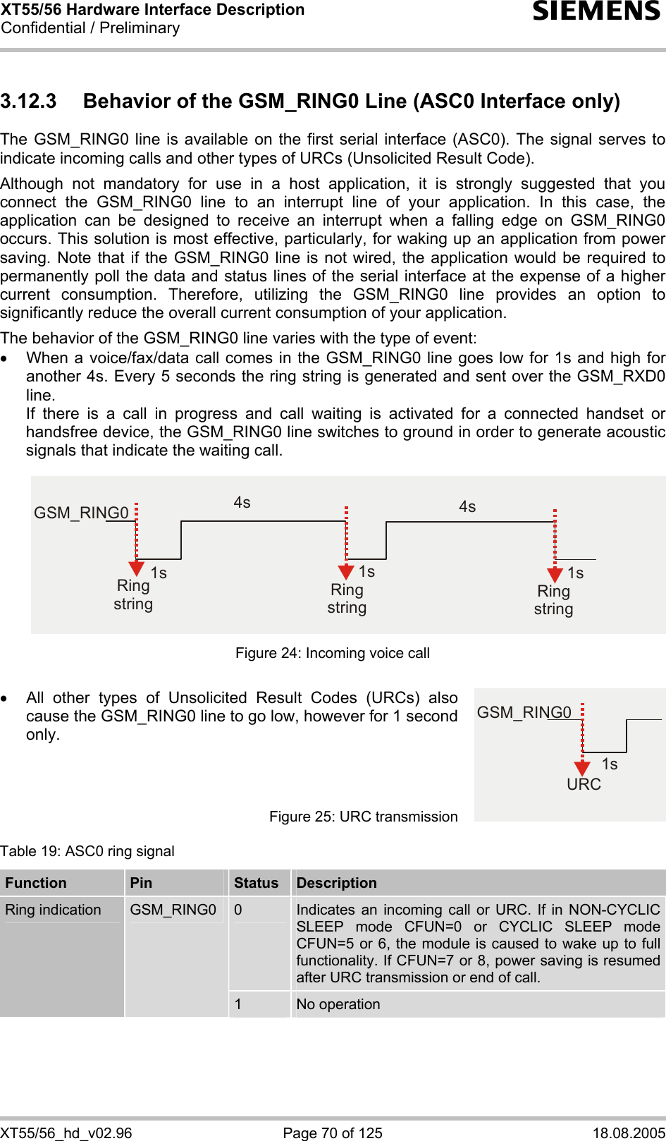
![XT55/56 Hardware Interface Description Confidential / Preliminary s XT55/56_hd_v02.96 Page 67 of 125 18.08.2005 3.12.2 Outputs 3.12.2.1 Synchronization Signal The synchronization signal serves to indicate growing power consumption during the transmit burst. The signal is generated by the GSM_SYNC pin. Please note that this pin can adopt two different operating modes which you can select by using the AT^SSYNC command (mode 0 and 1). For details refer to the following chapter and to [1]. To generate the synchronization signal the pin needs to be configured to mode 0 (= default). This setting is recommended if you want your application to use the synchronization signal for better power supply control. Your platform design must be such that the incoming signal accommodates sufficient power supply to the XT55/56 module if required. This can be achieved by lowering the current drawn from other components installed in your application. The timing of the synchronization signal is shown below. High level of the GSM_SYNC pin indicates increased power consumption during transmission. Figure 22: GSM_SYNC signal during transmit burst *) The duration of the GSM_SYNC signal is always equal, no matter whether the traffic or the access burst are active. Transmit burst1 Tx 577 µs every 4.616 ms2 Tx 1154 µs every 4.616 ms300 µsGSM_SYNC signal*)](https://usermanual.wiki/Telit-Cinterion-Deutschland/XT55.Updated-Usaer-Manual/User-Guide-585513-Page-67.png)
![XT55/56 Hardware Interface Description Confidential / Preliminary s XT55/56_hd_v02.96 Page 68 of 125 18.08.2005 3.12.2.2 Using the GSM_SYNC Pin to Control a Status LED As an alternative to generating the synchronization signal, the SYNC pin can be used to control a status LED on your application platform. Especially in the development and test phase of an application, system integrators are advised to use the LED mode of the SYNC pin in order to evaluate their product design and identify the source of errors. To avail of this feature you need to set the SYNC pin to mode 1 by using the AT^SSYNC command. For details see [1]. Table 18: Coding of the status LED LED mode Operating status of XT55/56 Permanently off XT55/56 is in one of the following modes: • POWER DOWN mode • ALARM mode • CHARGE-ONLY mode • NON-CYCLIC SLEEP mode • CYCLIC SLEEP mode with no temporary wake-up event in progress. 600 ms on / 600 ms off Limited Network Service: No SIM card inserted or no PIN entered, or network search in progress, or ongoing user authentication, or network login in progress. 75 ms on / 3 s off IDLE mode: The mobile is logged to the network (monitoring control channels and user interactions). No call in progress. 75 ms on / 75 ms off / 75 ms on / 3 s off One or more GPRS contexts activated. 0.5 s on / off depending on transmission activity Packet switched data transfer in progress. LED goes on within 1 second after data packets were exchanged. Flash duration is approximately 0.5 s. 75 ms URC Permanently on Depending on type of call: Voice call: Connected to remote party. CSD call: Connected to remote party or exchange of parameters while setting up or disconnecting a call. LED Off = SYNC pin low. LED On = SYNC pin high (if LED is connected as illustrated in Figure 23) Note: When a temporary wake-up event (URC, call, packet switched transfer) occurs in CYCLIC SLEEP mode the LED flashes. See Table 11 for details on the various SLEEP modes and wake-up events.](https://usermanual.wiki/Telit-Cinterion-Deutschland/XT55.Updated-Usaer-Manual/User-Guide-585513-Page-68.png)
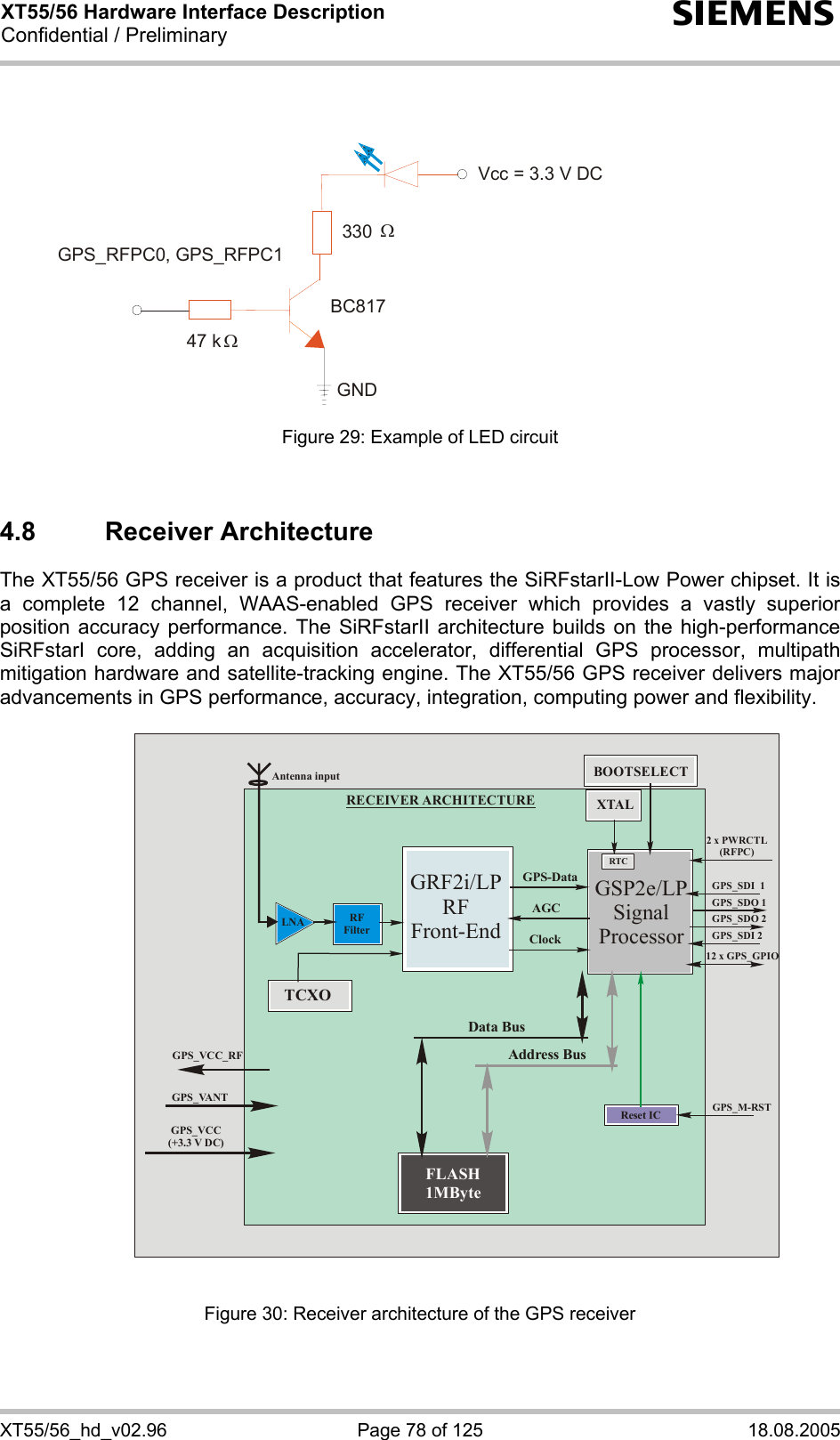
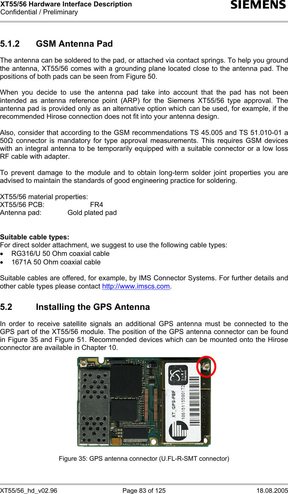
![XT55/56 Hardware Interface Description Confidential / Preliminary s XT55/56_hd_v02.96 Page 71 of 125 18.08.2005 4 GPS Application Interface The XT55/56 module integrates a GPS receiver which offers the full performance of GPS technology. The GPS receiver continuously tracks all satellites in view, thus providing accurate satellite position data. The GPS block can be used even if the XT55/56 module is deregistered from the GSM network. 4.1 Theory of Operation Figure 26: Theory of operation The XT55/56 GPS part is designed to use L1 Frequency (C/A Code) GPS receiver and performs the entire GPS signal processing, from antenna input to serial position data output. The processing steps involved are: • RF section In the RF section the GPS signal detected by the antenna is amplified, filtered and converted to an intermediate frequency (IF). An A/D converter transforms the analogue intermediate frequency into a digital IF signal. • GPS channels The received digital IF signal bit stream is passed to the baseband section, where it is fed into the correlators. The function of the correlators is to acquire and track the satellite signals. There are 12 channels used in parallel, with each correlator looking for a characteristic PRN code sequence in the bit stream. Once the correlator has found a valid signal, pseudo range, carrier phase and orbit information can be extracted from the GPS signal. • Navigation The on-board processor is running an algorithm that calculates the position, velocity and time. This calculation is called navigation solution. Once the navigation solution is calculated, it can be transformed into the desired coordinate system, e.g. Latitude/ Longitude/ Altitude. For further details refer to [4]. • Interface The data of the navigation solution are available at the serial RS-232 interface.](https://usermanual.wiki/Telit-Cinterion-Deutschland/XT55.Updated-Usaer-Manual/User-Guide-585513-Page-71.png)
![XT55/56 Hardware Interface Description Confidential / Preliminary s XT55/56_hd_v02.96 Page 72 of 125 18.08.2005 4.2 Technical Data Industry leading GPS performance • 12 channel GPS receiver • Signal acquisition using 1920 time / frequency search channels • Multipath-mitigation hardware • Cold start < 45 sec Low power • Typ. 220mW without active antenna (continuous mode) • TricklePower™ mode reduces power to < 60mW • Adaptive TricklePower™ switches between full and TricklePower™ • Push-to-Fix reduces power by as much as 98% Additional software options (can be obtained separately) • AVL (for further information refer to [4]) • SiRFXtrac (high sensitivity stand alone software) • SiRFDrive (high sensitivity dead reckoning software) Protocols • SDI1 / SDO1: NMEA 9600 baud, Msg.: GLL, GGA, RMC, VTG, GSV, GSA, ZDA 8 data bits, no parity, 1 stop bit • SDI2 / SDO2: RTCM, 9600 baud Specification • Position accuracy Autonomous: < 10 m Beacon DGPS: < 2.5 m • Receiver Tracking: L1, CA code Channels: 12 Max. update rate: 10 Hz Sensitivity: -142 dBm +2 dB 1) Max. altitude: <60.000 ft Max. velocity: <1.000 knots Protocol support: NMEA, SiRF binary • Acquisition rate SnapStart: < 3 sec Hotstart: < 8 sec Warmstart: < 38 sec Coldstart: < 45 sec 1) The specified GPS receiver sensitivity of the XT55/56 (GPS software version 2.3) in tracking mode is related to the ARP (antenna reference point). However, the applied antenna, the antenna amplifier, the customer application and / or the applied reference setup might cause variations of the stated receiver sensitivity value.](https://usermanual.wiki/Telit-Cinterion-Deutschland/XT55.Updated-Usaer-Manual/User-Guide-585513-Page-72.png)
![XT55/56 Hardware Interface Description Confidential / Preliminary s XT55/56_hd_v02.96 Page 73 of 125 18.08.2005 4.3 GPS Operating Modes Mode Function Normal operation The receiver is continuously running in Normal mode, as long as the operating voltage Vcc is supplied. Position fixes are generated at the maximum update rate. This enables the receiver a warm- and hotstart. However, the cold- and warmstart times of the receiver do not differ significantly under good visibility conditions. Trickle Power mode Vcc is continuously supplied to the receiver in Trickle Power mode. By using a especially configurable software, the user can force the receiver to acquire a position fix periodically. Between two fixes, the receiver will be in a low power mode. The power-on scenario in Trickle Power mode on the XT55/56 GPS part differs from one in continuous mode. If the receiver fails to acquire satellites within a given period of time (approx. 150 sec), the receiver enters an extended sleep phase. The duration of this sleep phase is approx. 30 sec. After that, the receiver wakes up, starts a reset and tries to acquire satellites. This procedure will be repeated until the GPS receiver can detect satellites. For further details refer to [1]. Push-to-Fix mode In this mode the receiver will turn on every 30 minutes to perform a system update consisting of a GPS RTC calibration and satellite ephemeris data collection if required (i.e. a new satellite has become visible) as well as all software tasks to support SnapSart in the event of an NMI. Ephemeris collection time in general takes 18 to 30 seconds. If ephemeris data is not required the system will recalibrate and shut down. In either case, the amount of time the receiver remains off will be in proportion to how long it stayed on: Off period = On Period*(1-Duty Cycle) Duty Cycle The off period has a possible range between 10 and 7200 seconds. The default is 1800 seconds.](https://usermanual.wiki/Telit-Cinterion-Deutschland/XT55.Updated-Usaer-Manual/User-Guide-585513-Page-73.png)
![XT55/56 Hardware Interface Description Confidential / Preliminary s XT55/56_hd_v02.96 Page 74 of 125 18.08.2005 4.3.1 Trickle Power Mode The default mode of XT55/56 GPS part is continuous mode, but the user can set the XT55/56 GPS part into the Trickle Power mode using the input command message. The XT55/56 GPS part enters the Trickle Power mode corresponding to Figure 27 (800ms OFF time and 200ms ON time) as soon as valid GPS data are available. As a result the average power consumption is reduced by approximately 80 % (approximately 150mW). The settings for the Trickle Power mode can be modified by using the SiRFstar demo software. For example if the XT55/56 GPS part is configured to enter the OnTime mode each 10s for a duration of 200ms the average power consumption can be reduced up to approx. 95% (approx. 15mW, ca. 4.8mA at Vcc=3.3V). For more details refer to [1]. Figure 27: Example for current in Trickle Power mode](https://usermanual.wiki/Telit-Cinterion-Deutschland/XT55.Updated-Usaer-Manual/User-Guide-585513-Page-74.png)
![XT55/56 Hardware Interface Description Confidential / Preliminary s XT55/56_hd_v02.96 Page 75 of 125 18.08.2005 4.3.2 Comparison of Trickle Power and Push-to-Fix Mode A comparison of the Trickle Power mode and Push-to-Fix mode is shown in Figure 28. This diagram shows that for position update intervals less than approximately 600 seconds (i.e. rates faster than one fix per 10 minutes), the Trickle Power mode at an update interval of 10 seconds offers a lower power solution. The user would then be required to filter the output position data to use only the data points corresponding to the desired update interval. For example, if the desired position output is at 60 second intervals, then the user would only need one out of every six position outputs at a 10 second Trickle Power update interval. Alternatively, the user could perform smoothing or averaging of the position data and provide an output at the desired rate. Please note that neither Trickle Power mode nor Push-to-Fix mode are supported if running XT55/56 AVL software. For further details regarding power supply ratings see [4]. Figure 28: Comparing typical current in Trickle Power and Push-to-Fix mode](https://usermanual.wiki/Telit-Cinterion-Deutschland/XT55.Updated-Usaer-Manual/User-Guide-585513-Page-75.png)
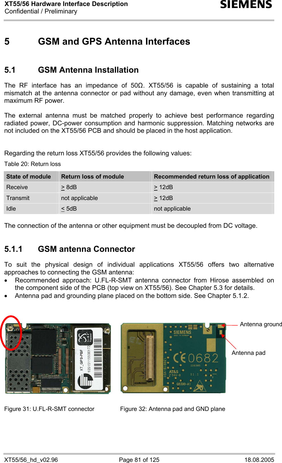
![XT55/56 Hardware Interface Description Confidential / Preliminary s XT55/56_hd_v02.96 Page 77 of 125 18.08.2005 4.6 Serial Interfaces of the XT55/56 GPS Part The GPS part of the XT55/56 module offers two serial interfaces: SD1 • 2-wire serial interface • Includes the SDI1 (receive) and SDO1 (transmit) lines • Supported baud rate: 9600…115200 bps. See also [1] for details on the used GPS protocol. SD2 • 2-wire serial interface • Includes the SDI2 (receive) and SDO2 (transmit) lines. It is intended for communication with the GSM/ GPRS part of the XT55/56 module. See Figure 2 for details. • Supported baud rate: 9600…115200 bps. See also [1] for details on the used GPS protocol. SD1 and SD2 • Both interfaces are configured for 8 data bits, no parity and 1 stop bit • For more detailed characteristics see [1] 4.7 GPS Control Signals GPS_M-RST: This pin provides an active-low reset input to the board. It causes the board to reset and start searching for satellites. Reset is an optional input and, if not utilized, it may be left open. GPS_BOOTSEL: Set this pin to high for reprogramming the flash of the XT55/56 GPS part (for instance updating to a new XT55/56 GPS firmware). GPS_RFPC0, GPS_RFPC1 (including pull-up resistors): These pins are input pins for Trickle-Power mode control. To use the Trickle-Power mode function connect the RFPC0 and RFPC1 as shown in Figure 58. The pull-up resistors ensure the correct voltage level during start-up and reset procedure of the GPS base band processor. GPS_GPIO8, GPS_GPIO4: These pins are control outputs for the Trickle-Power mode. GPS_GPIO8 must be connected to GPS_RFPC0 and GPS_GPIO4 to GPS_RFPC1. GPS_GPIO8, GPS_GPIO4 can also be used to control a LED. A possible circuit is shown in Figure 29. If the LED lights permanently the GPS receiver is searching for satellites. If the GPS receiver is in Trickle-Power mode, the LED flashes in rhythm, i.e. the GPS receiver receives valid position data. Timing differs between GPS_GPIO4 and GPS_GPIO8. Note: If Trickle power is switched off the LED lights permanently.](https://usermanual.wiki/Telit-Cinterion-Deutschland/XT55.Updated-Usaer-Manual/User-Guide-585513-Page-77.png)
![XT55/56 Hardware Interface Description Confidential / Preliminary s XT55/56_hd_v02.96 Page 103 of 125 18.08.2005 6.5 Electrical Characteristics of the Voiceband Part 6.5.1 Setting Audio Parameters by AT Commands The audio modes 2 to 6 can be adjusted according to the parameters listed below. Each audio mode is assigned a separate set of parameters. Table 30: Audio parameters adjustable by AT command Parameter Influence to Range Gain range Calculation inBbcGain MICP/MICN analog amplifier gain of baseband controller before ADC 0...7 0...42dB 6dB steps inCalibrate digital attenuation of input signal after ADC 0...32767 -...0dB 20 * log (inCalibrate/ 32768) outBbcGain EPP/EPN analog output gain of baseband controller after DAC 0...3 0...-18dB 6dB steps outCalibrate[n] n = 0...4 digital attenuation of output signal after speech decoder, before summation of sidetone and DAC present for each volume step[n] 0...32767 -...+6dB 20 * log (2 * outCalibrate[n]/ 32768) sideTone digital attenuation of sidetone is corrected internally by outBbcGain to obtain a constant sidetone independent of output volume 0...32767 -...0dB 20 * log (sideTone/ 32768) Note: The parameters inCalibrate, outCalibrate and sideTone accept also values from 32768 to 65535. These values are internally truncated to 32767.](https://usermanual.wiki/Telit-Cinterion-Deutschland/XT55.Updated-Usaer-Manual/User-Guide-585513-Page-103.png)
![XT55/56 Hardware Interface Description Confidential / Preliminary s XT55/56_hd_v02.96 Page 104 of 125 18.08.2005 6.5.2 Audio Programming Model The audio programming model shows how the signal path can be influenced by varying the AT command parameters. The model is the same for all three interfaces, except for the parameters <outBbcGain> and <inBbcGain> which cannot be modified if the digital audio interface is being used, since in this case the DAC is switched off. The parameters inBbcGain and inCalibrate can be set with AT^SNFI. All the other parameters are adjusted with AT^SNFO. ADAD-∞...0dBSpeech coderneg. gain (attenuation) 0dB; -6db, -12dB; -18dB +0...42dB in 6dB steps 1k 1k 1k 1k 2.65V 10uF + <sideTone> AT parameters are given in brackets <…> and marked red and italic. <outCalibrate[n]> n = 0...4 <inCalibrate> <inBbcGain> <outBbcGain> Speech decoderGSM_MIC2 GSM_TFSDAI, GSM_TXDDAI GSM_RFSDAI, GSM_RXDDAI GSM_MIC1 <io><ep><mic> Figure 48: AT audio programming model](https://usermanual.wiki/Telit-Cinterion-Deutschland/XT55.Updated-Usaer-Manual/User-Guide-585513-Page-104.png)
![XT55/56 Hardware Interface Description Confidential / Preliminary s XT55/56_hd_v02.96 Page 105 of 125 18.08.2005 6.5.3 Characteristics of Audio Modes The electrical characteristics of the voiceband part depend on the current audio mode set with the AT^SNFS command. Table 31: Voiceband characteristics (typical) Audio mode no. AT^SNFS= 1 (Default settings, not adjustable) 2 3 4 5 6 Name Default Handset Basic Handsfree Headset User Handset Plain Codec 1 Plain Codec 2 Purpose DSB with Votronic handset Siemens Car Kit Portable Siemens Headset DSB with individual handset Direct access to speech coder Direct access to speech coder Gain setting via AT command. Defaults: inBbcGain outBbcGain Fix 4 (24dB) 1 (-6dB) Adjustable 2 (12dB) 1 (-6dB) Adjustable 5 (30dB) 2 (-12dB) Adjustable 4 (24dB) 1 (-6dB) Adjustable 0 (0dB) 0 (0dB) Adjustable 0 (0dB) 0 (0dB) Default audio interface 1 2 2 1 1 2 3) Power supply ON (2.65V) ON (2.65V) ON (2.65V) ON (2.65V) OFF (GND) OFF (GND)Sidetone ON --- Adjustable Adjustable Adjustable Adjustable Volume control OFF Adjustable Adjustable Adjustable Adjustable Adjustable Limiter (receive) ON ON ON ON --- --- Compressor (receive) --- OFF1) --- --- --- --- AGC (send) --- --- ON --- --- --- Echo control (send) Suppression Cancellation +suppression --- Suppres-sion --- --- Noise suppression2) --- up to 10dB 10dB --- --- --- MIC input signal for 0dBm0 @ 1024 Hz (default gain) 23mV 58mV 7.5mV @ -3dBm0 due to AGC 23mV 315mV 315mV EP output signal in mV rms. @ 0dBm0, 1024 Hz, no load (default gain); @ 3.14 dBm0 284mV 120mV default @ max volume 300mV default @ max volume 284mV default @ max volume 895mV 3.7Vpp 895mV 3.7Vpp Sidetone gain at default settings 22.8dB - dB Affected by AGC, 13dB @ 7.5mV (MIC) 22.8dB - dB - dB 1) Adaptive, receive volume increases with higher ambient noise level. The compressor can be activated by loading an application specific audio parameter set (see [10]). 2) In audio modes with noise reduction, the microphone input signal for 0dBm shall be measured with a sine burst signal for a tone duration of 5 seconds and a pause of 2 sec. The sine signal appears as noise and, after approx. 12 sec, is attenuated by the noise reduction by up to 10dB.](https://usermanual.wiki/Telit-Cinterion-Deutschland/XT55.Updated-Usaer-Manual/User-Guide-585513-Page-105.png)
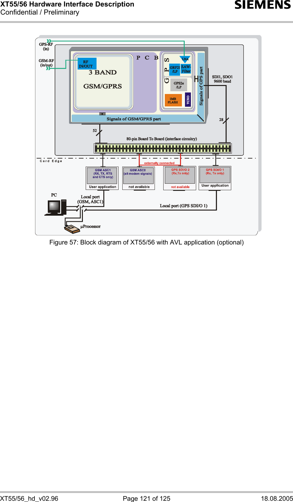
![XT55/56 Hardware Interface Description Confidential / Preliminary s XT55/56_hd_v02.96 Page 120 of 125 18.08.2005 9 Example Applications The XT55/56 module offers different options for integrating additional software, such as AVL and SiRF Demo software. For further details refer to [1] and [4]. Figure 56: Block diagram of XT55/56 for SiRF Demo application](https://usermanual.wiki/Telit-Cinterion-Deutschland/XT55.Updated-Usaer-Manual/User-Guide-585513-Page-120.png)