Telit Communications S p A DE921 CDMA Module User Manual
Telit Communications S.p.A. CDMA Module Users Manual
UserManual.wiki
>
Telit Communications S p A
>
DE921 User Manual
Users Manual
Navigation menu
Upload a User Manual
Namespaces
Wiki Guide
HTML
PDF
Info
Views
User Manual
Discussion / Help
Navigation

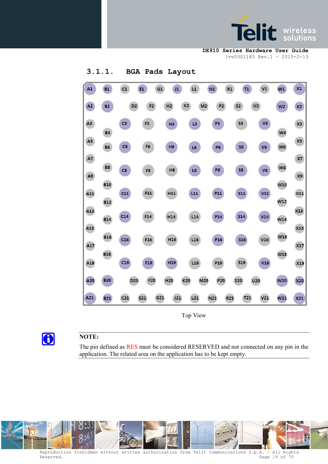
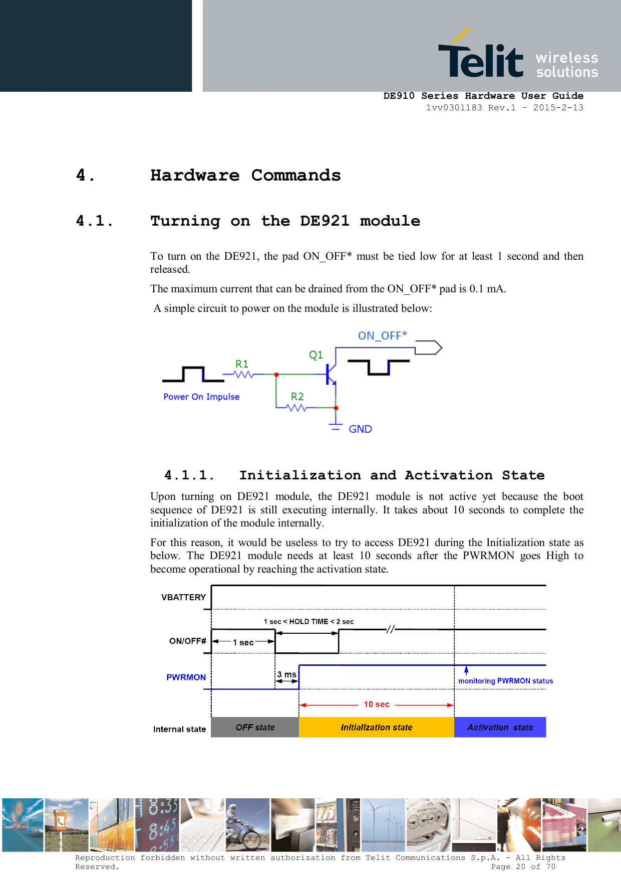
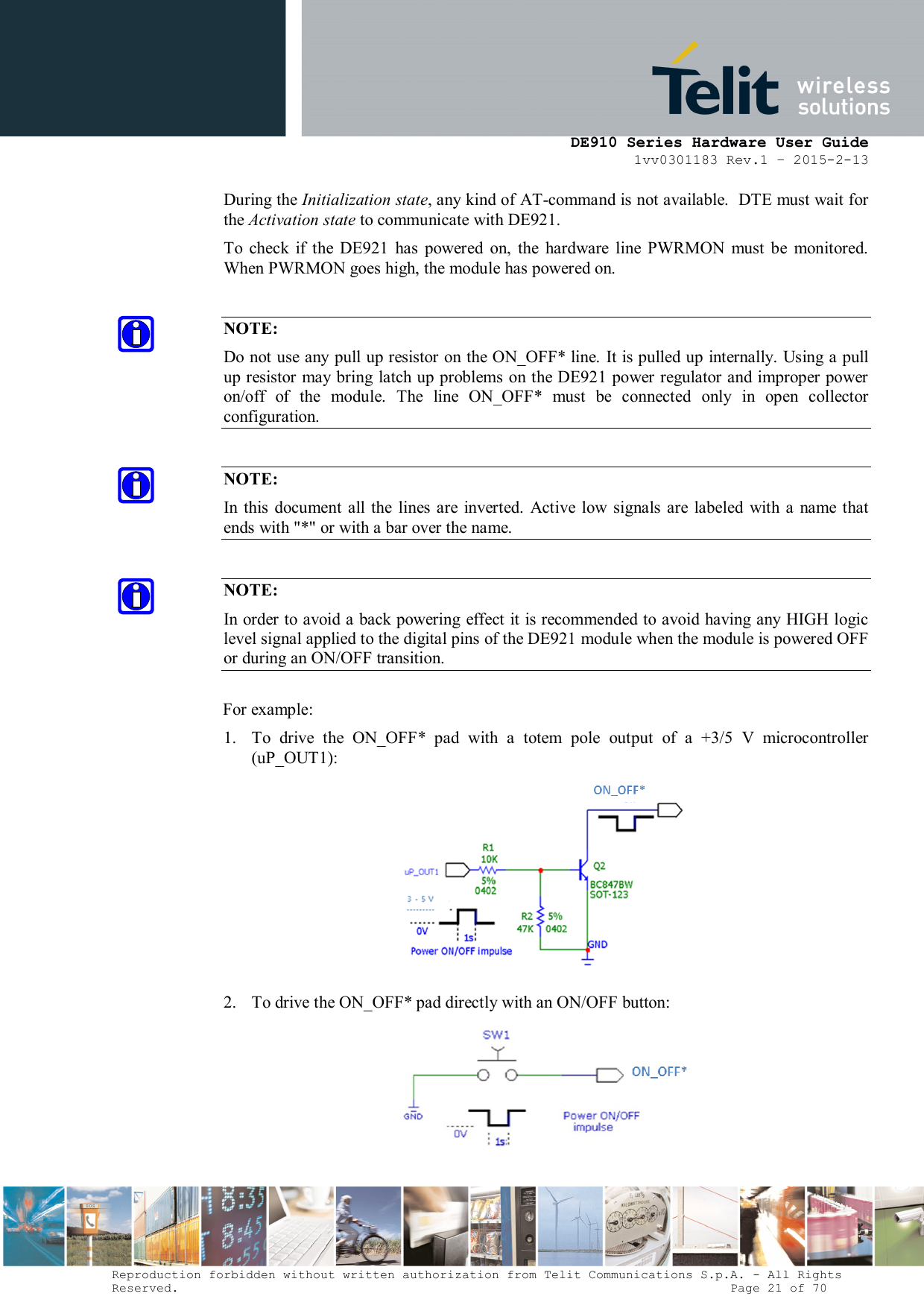
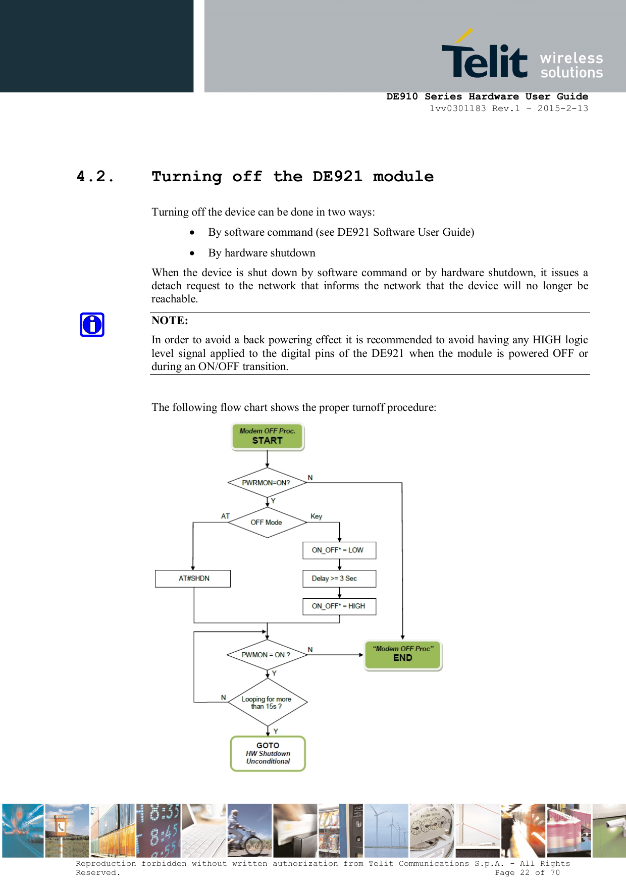

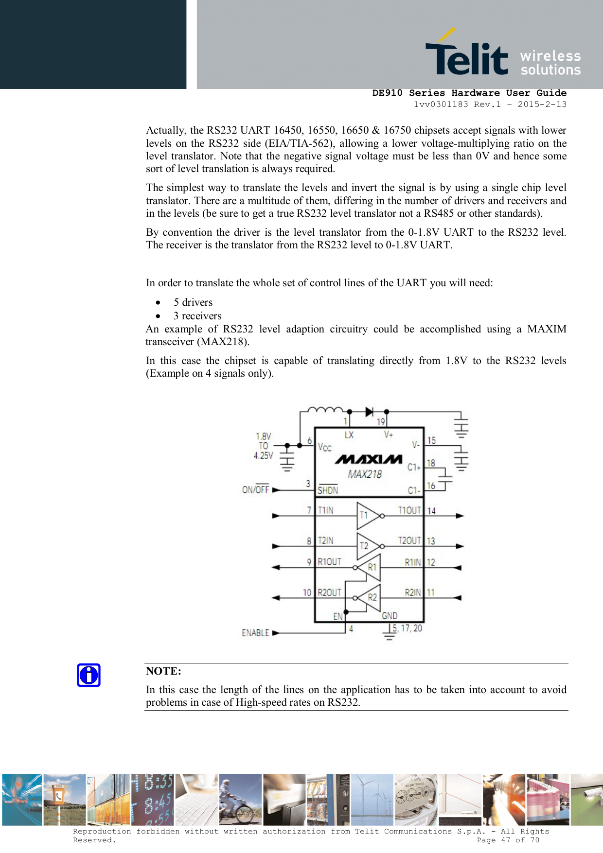
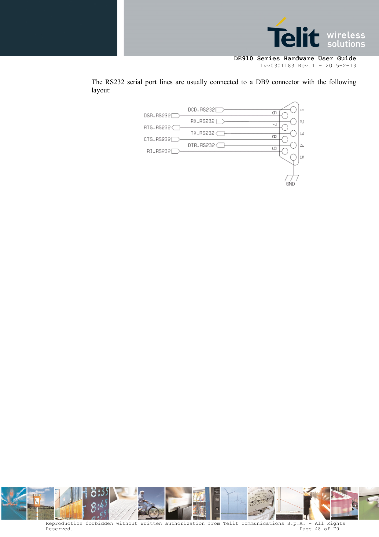
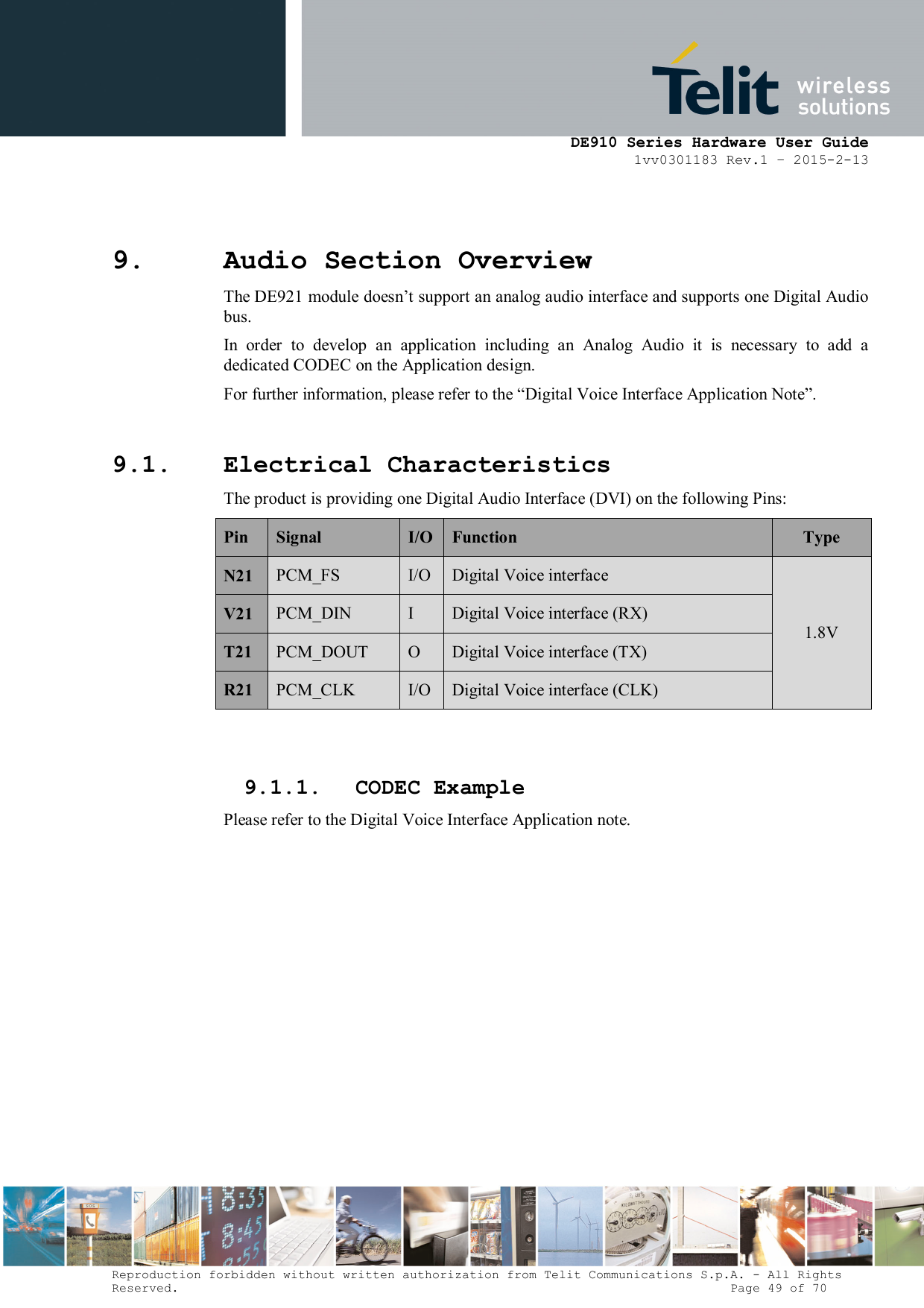
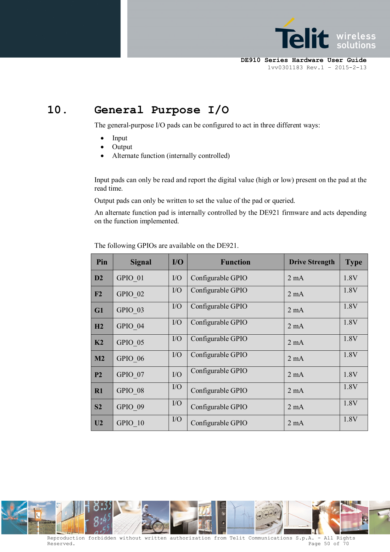
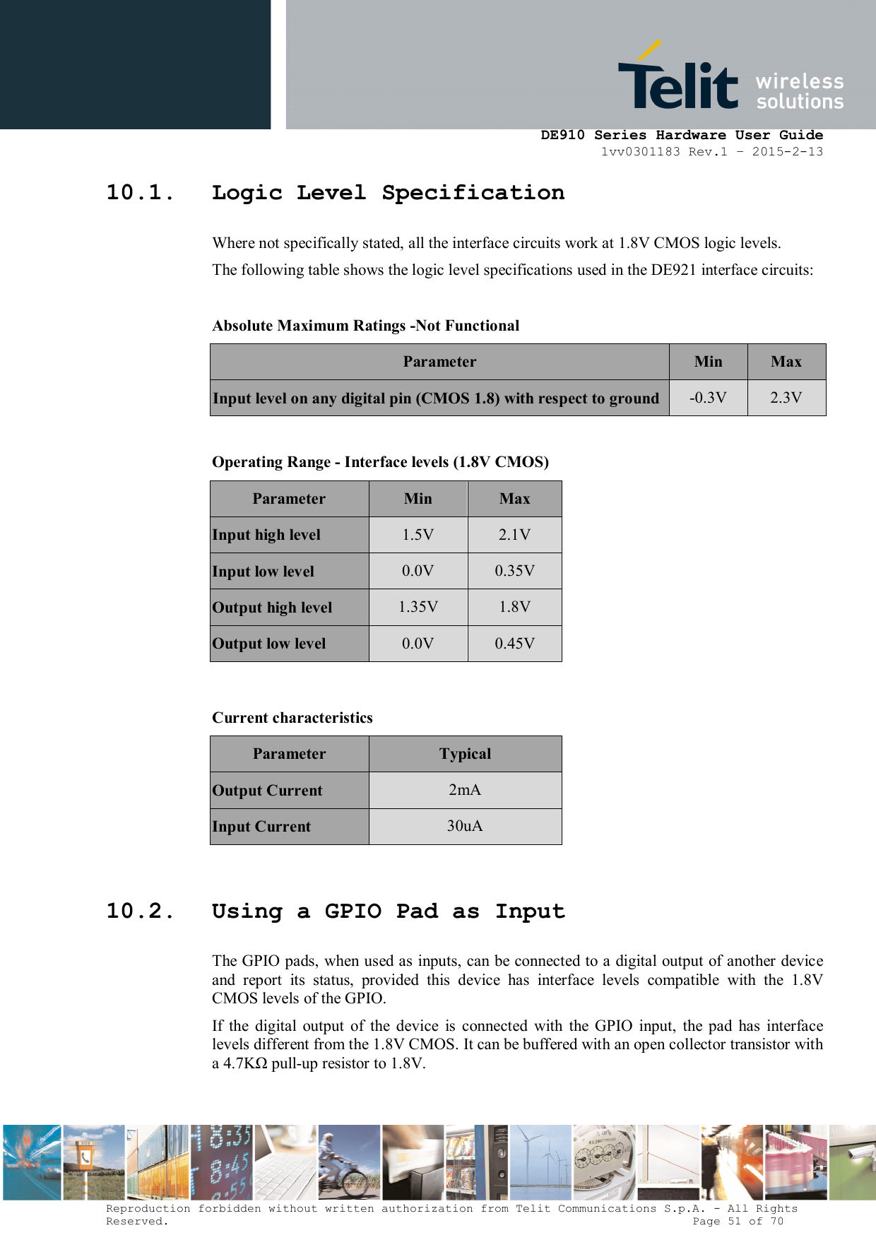
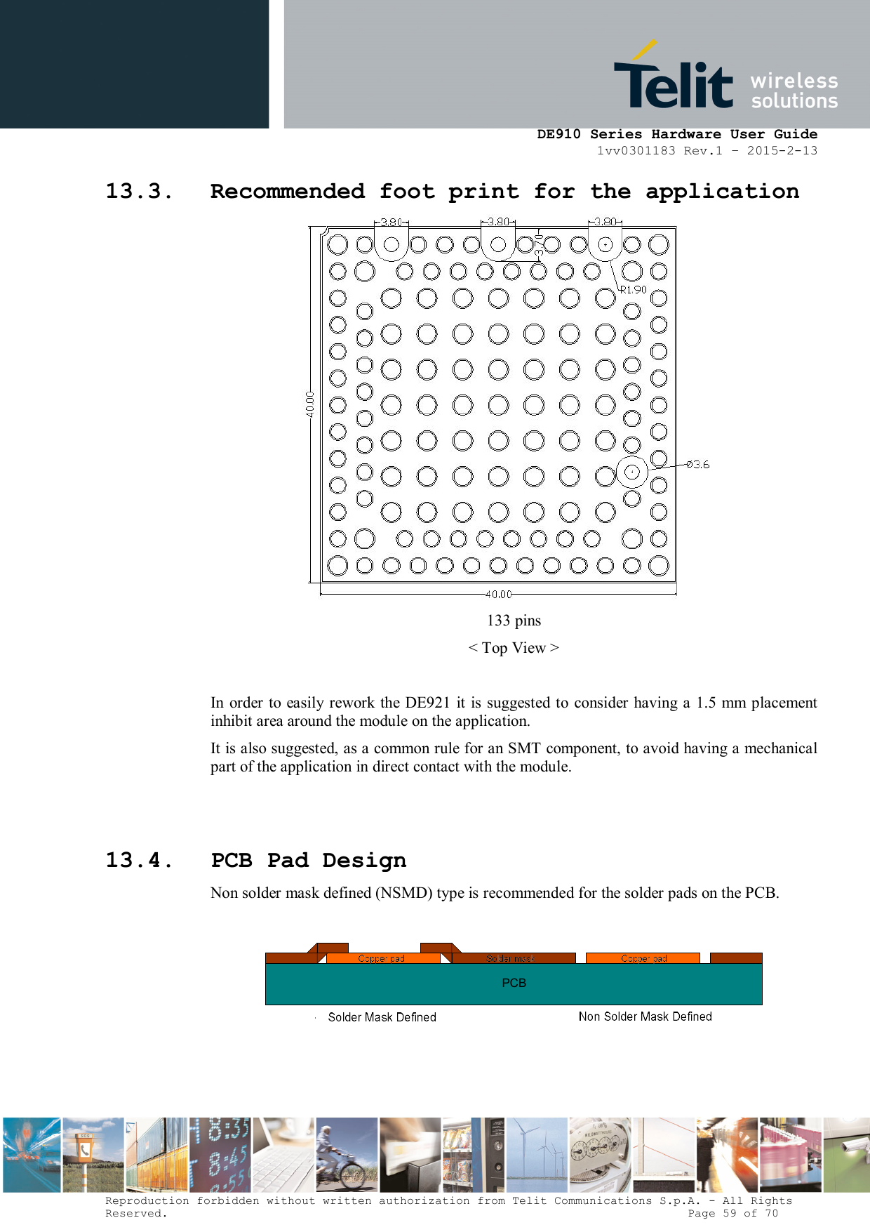
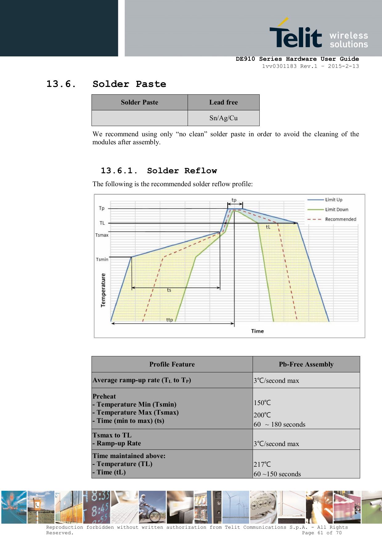
![DE910 Series Hardware User Guide 1vv0301183 Rev.1 – 2015-2-13 Reproduction forbidden without written authorization from Telit Communications S.p.A. - All Rights Reserved. Page 60 of 70 13.5. Recommendations for PCB Pad Dimensions (mm) It is not recommended to place via or micro-via not covered by solder resist in an area of 0.3 mm around the pads unless it carries the same signal as the pad itself (see following figure). Description Diameter [mm] Solder resist opening A 1.9 Except for ANT and VBATT 2.3 Metal pad B 1.6 2.0 Holes in pad are allowed only for blind holes and not for through holes. Recommendations for PCB Pad Surfaces: Finish Layer thickness (um) Properties Electro-less Ni / Immersion Au 3 ~ 7 / 0.05 ~ 0.15 good solder ability protection, high shear force values The PCB must be able to resist the higher temperatures which are occurring at the lead-free process. This issue should be discussed with the PCB-supplier. Generally, the wettability of tin-lead solder paste on the described surface plating is better compared to lead-free solder paste.](https://usermanual.wiki/Telit-Communications-S-p-A/DE921/User-Guide-2690261-Page-60.png)