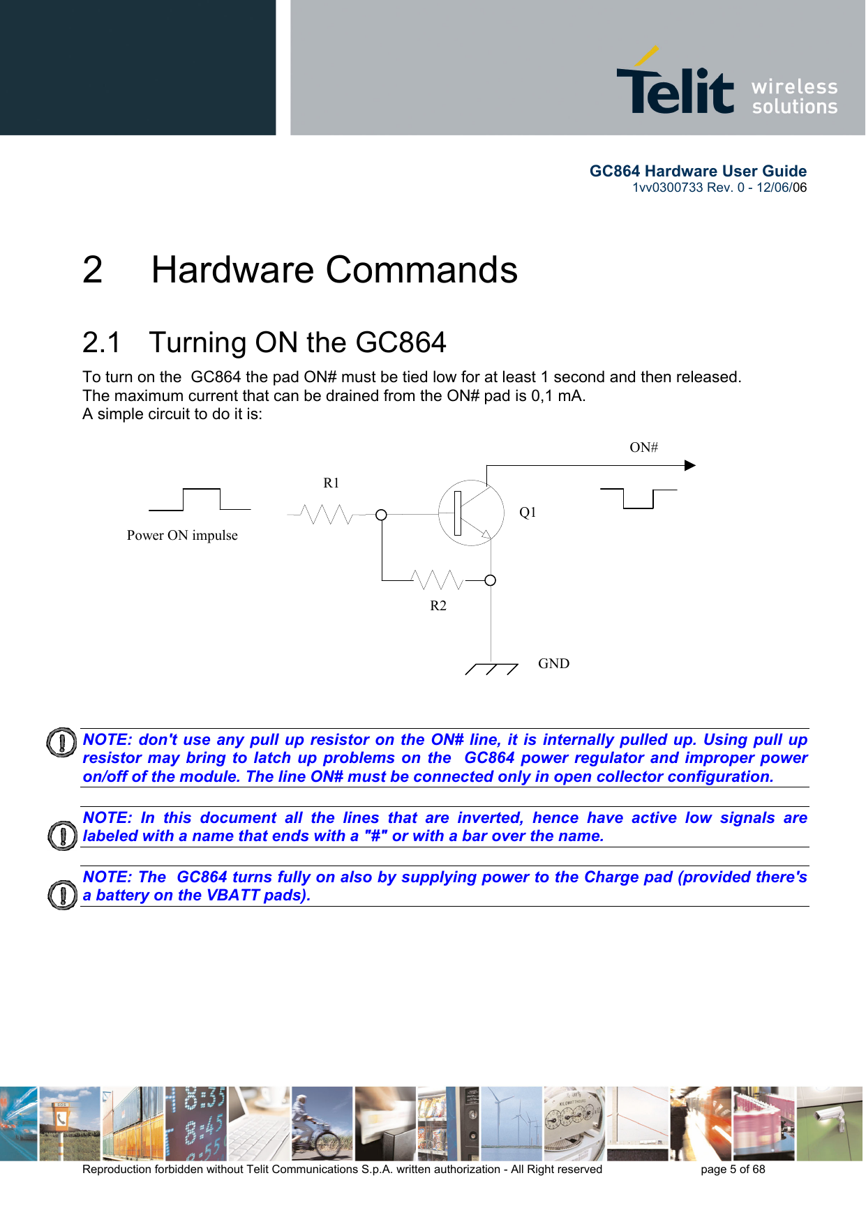
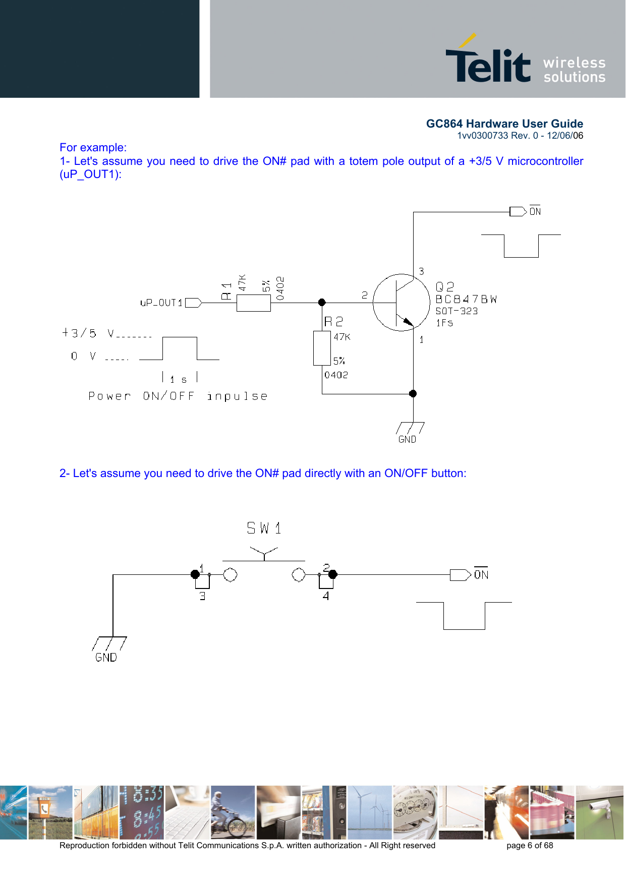
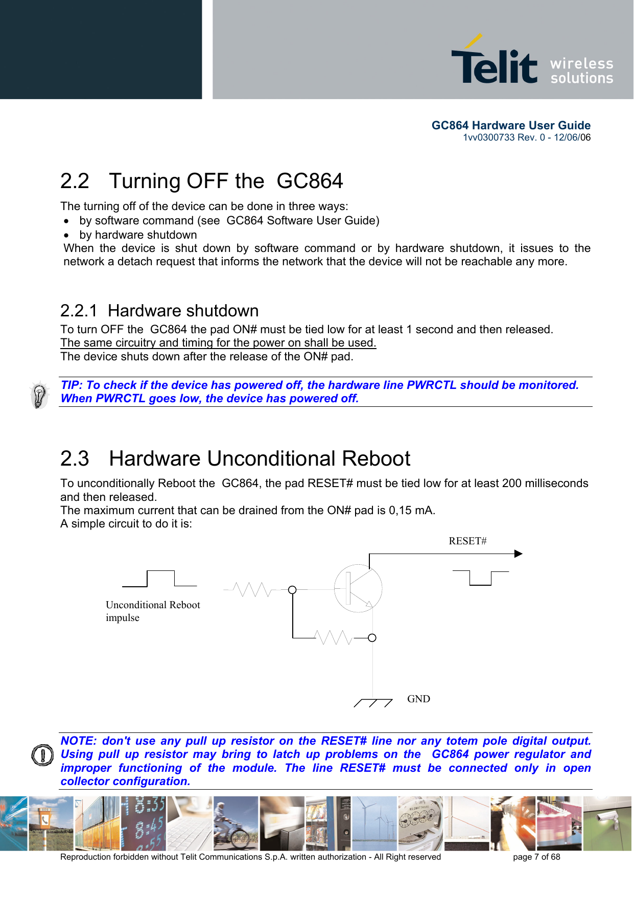
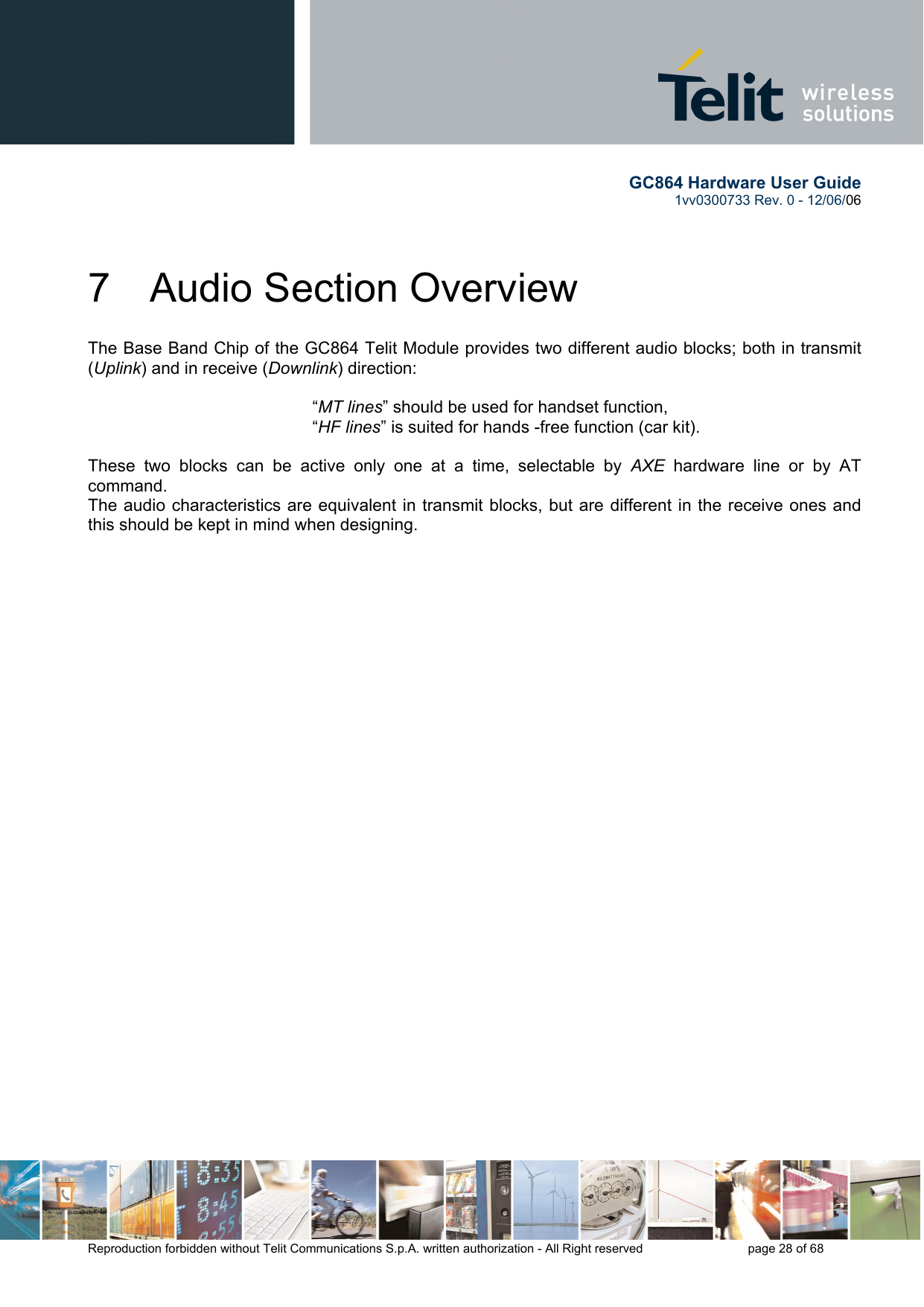
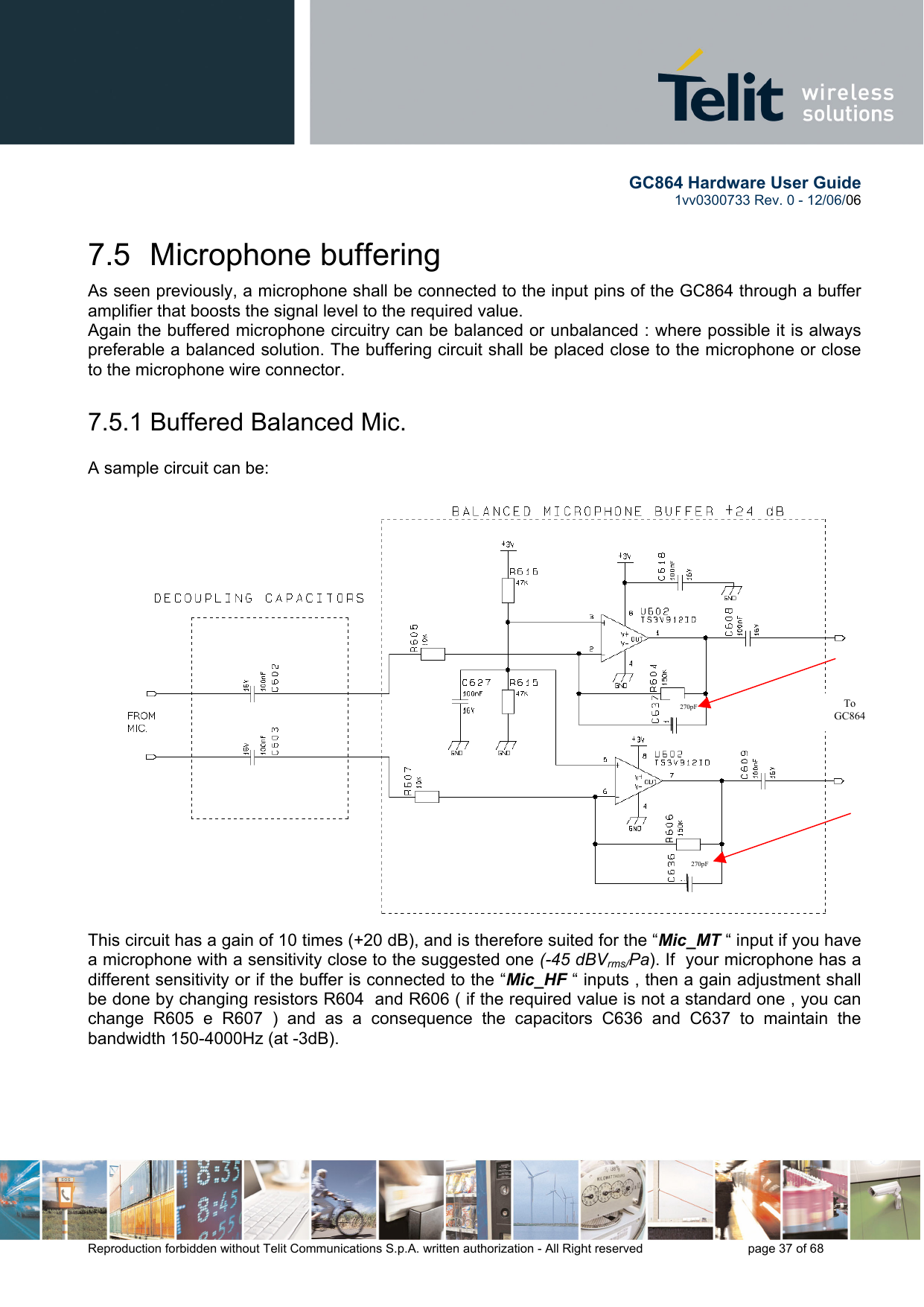
Telit Communications S p A GC864 Quad-Band GSM/GPRS module - Type: GC864 User Manual GC864 Hardware User Guide
Telit Communications S.p.A. Quad-Band GSM/GPRS module - Type: GC864 GC864 Hardware User Guide
UserManual.wiki
>
Telit Communications S p A
>
GC864 User Manual
Users Manual
Navigation menu
Upload a User Manual
Namespaces
Wiki Guide
HTML
PDF
Info
Views
User Manual
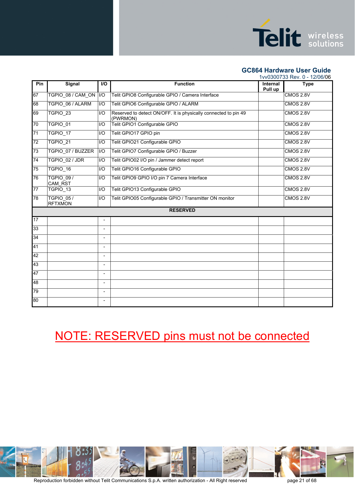
Discussion / Help
Navigation


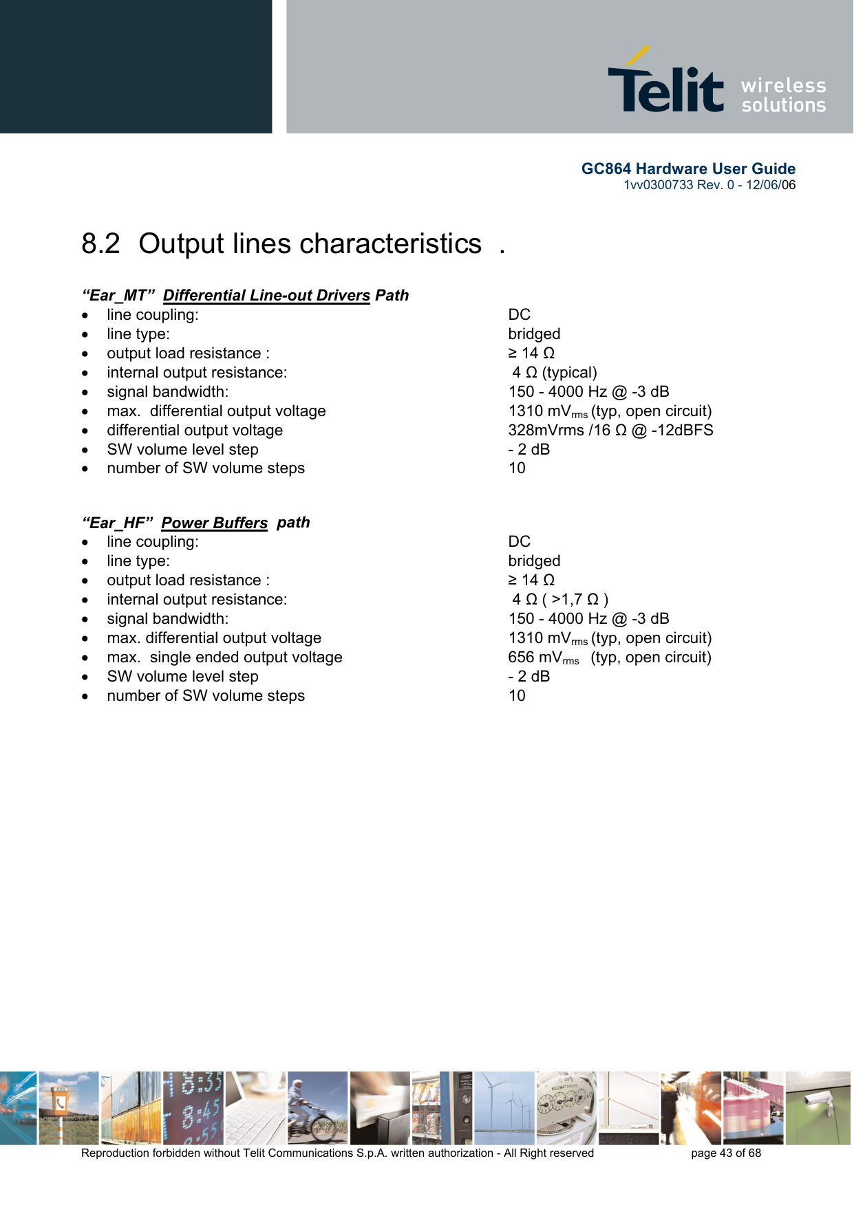
![GC864 Hardware User Guide 1vv0300733 Rev. 0 - 12/06/06 Reproduction forbidden without Telit Communications S.p.A. written authorization - All Right reserved page 31 of 68 TIP: definition of the nominal sensitivity of the microphone lines . The nominal sensitivity of the microphone lines indicates the voltage level on the GC864 pins present during "normal spoken" conditions. For a handset , the "normal spoken” conditions take place when the talker mouth is 7cm far from the microphone ; under these conditions the voice will produce an acoustic pressure of -4,7dBPa @1kHz on the microphone membrane . TIP: electrical equivalent signal and operating voice levels . At "normal spoken" conditions, a microphone having the suggested nominal sensitivity of -45dBVrms/Pa , will produce the electrical equivalent signal : that means : During a call , this level varies according to the volume of the talker voice; usually the following rough thumb rule for the dynamic range may be used : 1) the talker is screaming . This is the strongest voice level condition : the signal increases by +20dB ; 2) the talker is whispering. This is the lowest voice level condition: the voice level decreases by –50dB . These changes must be considered for designing the external microphone amplifier . TIP: example of external microphone amplifier calculation . Let’s suppose to use the 1stdifferential microphone path .In this case the maximum differential input voltage to “Mic_MT” lines is 365mVrms(1,03Vpp) corresponding to –8,76dBV. Now we can calculate the maximum voltage gain of an external microphone amplifier GA : ()[]dBVGdBMicLevel A76,820 −=++ []76,8207,49 −=++− AG AG−=+− 209,40 dBGA94,20= you can set GA= +20dB to use standard resistor values . MicLevel = ( -45) + (-4.7) = -49.7 dBVrms MicVoltage = 10 ( -49.7 / 20 ) = 3.3* 10 -3 Vrms](https://usermanual.wiki/Telit-Communications-S-p-A/GC864/User-Guide-687742-Page-31.png)
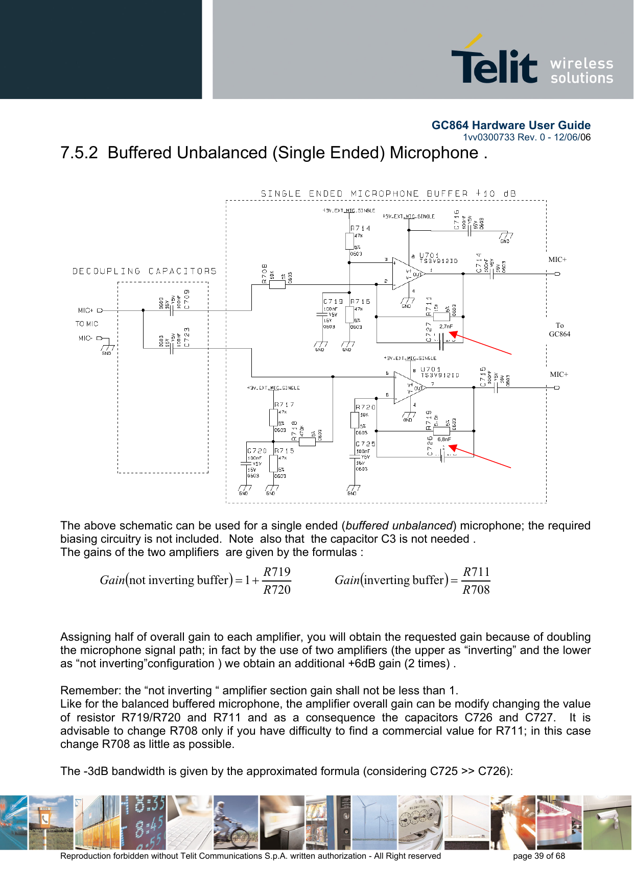
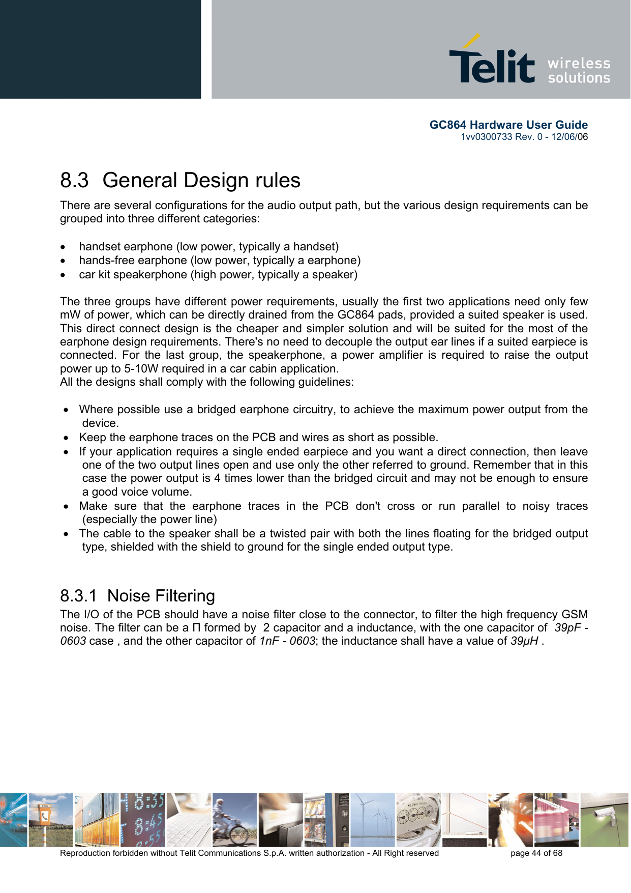
![GC864 Hardware User Guide 1vv0300733 Rev. 0 - 12/06/06 Reproduction forbidden without Telit Communications S.p.A. written authorization - All Right reserved page 38 of 68 The buffer gain is given by the formula: 607606605604RRRRGain == The C636 and C637 capacitors are placed in order to cut off the gain at higher frequencies than the transmitted GSM band, the cutoff frequency (-3dB) should be 3500Hz in order to have -1dB at 3kHz. The cutoff frequency is given by the formula: 636*606*21637*604*21.CRCRfreqππ== [Hz] TIP: example of calculation . Let's assume you have a microphone with a sensitivity of -45 dBVrms/Pa and you want to use it in 1st differential microphone path (“Mic_MT” inputs) in "normal spoken" conditions at acoustic pressure of -4.7dBPa. As reported at page 33 , the electrical level output from the microphone will be : corresponding to: When the talker is screaming ,we will have a signal of 330 mVrms on the “Mic_MT “ inputs for a buffer gain GA : GA =20 log (AmplifierOutput / MicVoltage) =20 log (330 * 10 -3 )/( 3.3 * 10 -3 ) = 20 log 10=20dB The corresponding values for the resistors on the buffer could be ( if we keep the input resistance 10kΩ ) R604 = R606 = gain* R603= gain* R605 = 10* 15 = 150 kΩ The commercial values of 150kΩ & 15kΩ are then chosen. As a consequence the values of the capacitors C636 and C637 shall be: C636=C637= 1/ (2π*4000*R606)= 265 *10 -12 F A commercial value of 270pF gives a cutoff frequency of 3931Hz with an errorless than 1,8% . MicLevel = ( -45) + (-4.7) = -49.7 dBVrms MicVoltage = 10 ( -49.7 / 20 ) = 3.3* 10 -3 Vrms](https://usermanual.wiki/Telit-Communications-S-p-A/GC864/User-Guide-687742-Page-38.png)
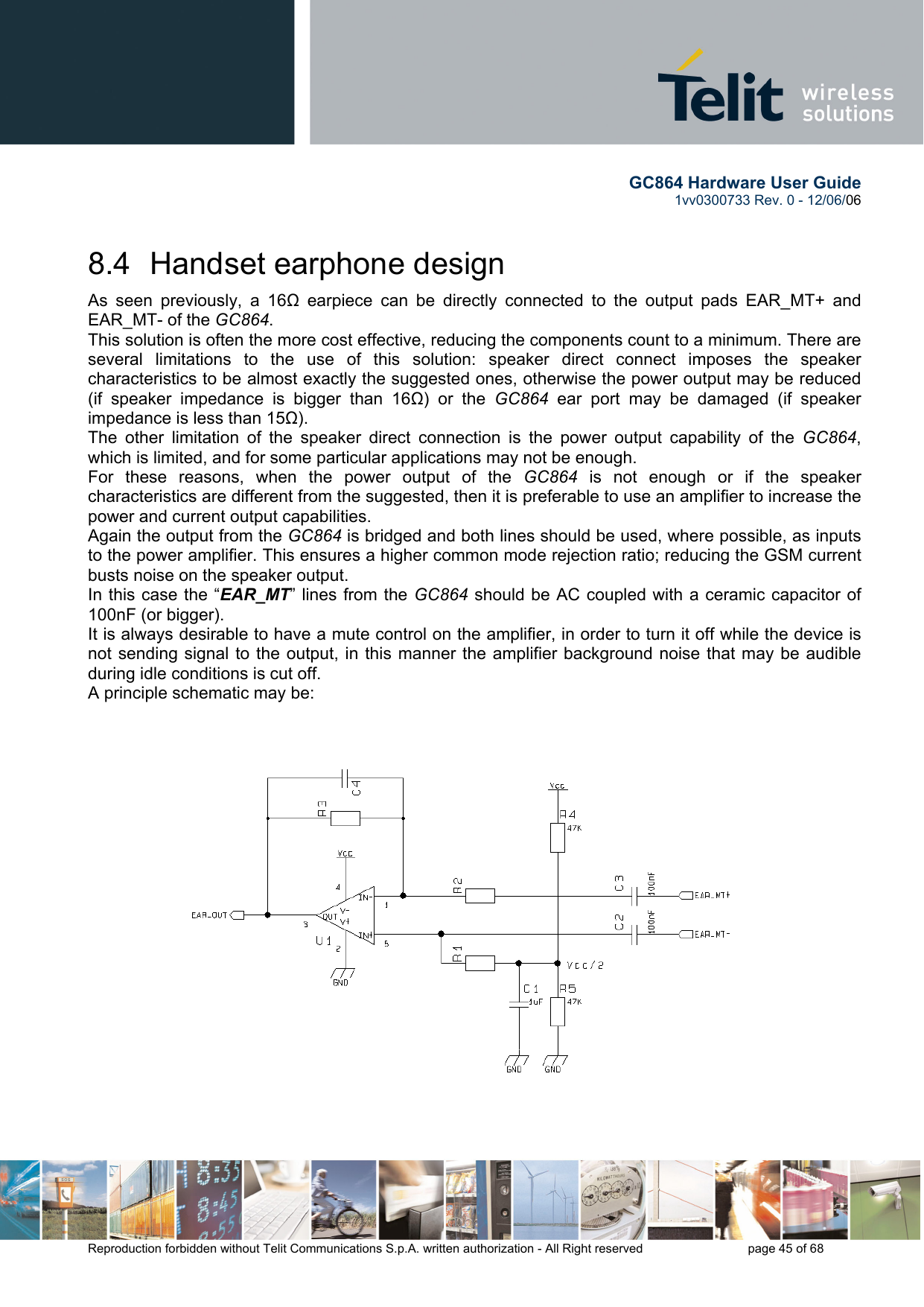
![GC864 Hardware User Guide 1vv0300733 Rev. 0 - 12/06/06 Reproduction forbidden without Telit Communications S.p.A. written authorization - All Right reserved page 40 of 68 727*711*21726*719*21.CRCRfreqππ== [Hz] The buffer bandwidth at -3dB shall be 4KHz. Note that the biasing of the operational amplifier is given for the inverting amplifier by the series divider R714-R715. The 100nF capacitor C719 is needed to filter the noise that could be coupled to that divider. For the not inverting operational amplifier the biasing is given by a different divider R715-R717 with the capacitor C720 and through a series resistor R718 of 470KΩ. TIP: example of calculation. Llet's assume you have a microphone with a sensitivity of -45dBVrms/Pa and you want to use it in 2nd differential microphone path (“Mic_HF” inputs) in "normal spoken" conditions at acoustic pressure of -4.7dBPa. As reported at page XX , the electrical level output from the microphone will be : but we have to consider 20dB loss due to the higher distance from the mouth of the talker ( 50cm ) . corresponding to In order to have a signal of 1 mVrms at the “Mic_HF” inputs , as suggested at TIP “environment consideration “, the buffer must have a gain or +10 dB Keeping in mind that “ balancing the line will double the signal”, to calculate the resistor values assign half of required gain GA to each amplifier section . And therefore GS =1,5times (or +3,52dB) . Choosing as 10kΩ as the input resistance , the corresponding values for the resistors on the buffer will be : R711 = GS * R708= 1.5*10 =15 kΩ R719 = (GS -1) * R720 = (1.5 -1)*10 =5 kΩ The commercial values of 15kΩ and 5.6kΩ be accepted . MicLevel = ( -45) + (-4.7) = -49.7 dBVrms MicVoltage = 10 ( -69.7 / 20 ) = 0,33* 10 -3 MicLevel = ( -49.7) + (-20) = -69.7 dBVrmsGA= “Mic_HF /MicVoltage = (1*10 -3)/(0,33*10 3](https://usermanual.wiki/Telit-Communications-S-p-A/GC864/User-Guide-687742-Page-40.png)
![GC864 Hardware User Guide 1vv0300733 Rev. 0 - 12/06/06 Reproduction forbidden without Telit Communications S.p.A. written authorization - All Right reserved page 46 of 68 The resulting gain and high pass cut can be obtained with the formula: 23RRGain = 4*3*21.CRfreqπ= [Hz] And an example of internal Ear amplifier could be: Some amplifier require a low impedance load at high frequency in order to avoid auto oscillation, this can be made with a capacitor (100nF) in series with a resistor (15Ω). When designing your application, remember to provide an adequate bypass capacitor to the amplifier and place it close to the power input pin of the IC, keeping the traces as short as possible. 8.5 Hands-free earphone (low power) design The same design considerations made for the handset are valid for the hands-free earphone. +12dBGC864](https://usermanual.wiki/Telit-Communications-S-p-A/GC864/User-Guide-687742-Page-46.png)


![040247K5%noMount=YESR111L18ALP2982AIM5X–2_8–NOPBMA05AU1021V_IN3ON–OFF4BYPASS5V_OUT2GNDIICSCL/AGILENT6BCAM_SCL/IIC_SCL9BCAM_M_CLK10D;5ACAM_M_CLK5A;5CCAM_SDA/IIC_SDA5D;6BTP101TP106GNDVAUX1TP105GND04021K5%R104GNDTP108VAUX1TP110040200noMount=YESR113GNDGNDGNDJP11625V040215nFX7RnoMount=YESC106JP120JP10910VCONT–A10uFC104FORBIDDENVIETATEALL RIGHTS RESERVEDRIPRODUZIONE E DIVULGAZIONE REPRODUCTION AND DISCLOSURETUTTI I DIRITTI RISERVATIPROJECTA3DESCRIPTIONDRAWING CODEFORMMODIFYOF SHEETSDATESHEET N.VERIFIEDPROJECTDRAWNPATH /home/users/areaMod. 067 rev.1 11/02 ANNOTATIONFILE NAMEBCDEA42 98 1071 3 1165040247K5%noMount=YESR110VCC_MAIN_CAM6.3V06032.2uFX5RC109CAM_DRDY/AGILENT6BPD[5]5A4773540103470SO107213PD[1]5AJP106JP107GNDGNDGNDTP109040200R115040200R112PD[0]5APD[2]5A040200R10610V0402100nFY5VC1126BCAM_PWR_ON/AGILENTVCC_MAIN_CAMSN74LVC1G08DCKRU1015VCC3GNDTGPIO_08/CAM_ON9BPD[4]5AJP114040200R105CAM_SYNC/AGILENT5AMON1/CAM_CLK10DPD[3]5APD[6]5AVCC_MAIN_CAMCAM_SDA/IIC_SDA6B;9B4773540103470SO109213TP10225V040215nFX7RC10525V040215nFX7RnoMount=YESC111TGPIO_08/CAM_ON5D040200R109noMount=YES52437–2472SO105321456789101112131415161718192021222324CAM_SCL/IIC_SCL5CTP1114773540103470SO106213TP107TGPIO_09/CAM_RST5COT101JP105JP1174779723130417SO102321456789101112131415161718192021222324252627282930040200R114SN74LVC1G08DCKRCEU101241040200R116040200R1084779723130417SO101321456789101112131415161718192021222324252627282930TP1046.3V06032.2uFX5RC11050V040233pFCOGC107GNDPD[7]5BCAM_PWR_ON/AGILENT6B6.3V06032.2uFX5RC108GNDJP108TGPIO_09/CAM_RST9B040200R1070402100K5%R103GNDGNDJP112TP112TP103JP1214773540102470noMount=YESSO10421JP110GND4773540103470SO108213MON1/CAM_CLK9B10276Furlan M. 0609051 30276SE11170Pasqualini N.cs1170.cir I2CBUS DUAL CAMERA060905SCLKRESET_NDVDD28ShieldSDINPS1VALIDHAVDD28VCLKOUTLED_CTRLTransChip TC5747MF24L (24pin)VALIDVPS2AGNDDGNDCLK_ININTERFACE CONNECTORSTC5747MF24LDOUT1DOUT3DOUT2DOUT0DOUT6DOUT4DOUT5DOUT7DOUT8GM862TRIZIUM– 1 –](https://usermanual.wiki/Telit-Communications-S-p-A/GC864/User-Guide-687742-Page-66.png)