Telit Communications S p A GC864Q2 Quadband GSM/ GPRS Module User Manual GC864 Hardware User Guide
Telit Communications S.p.A. Quadband GSM/ GPRS Module GC864 Hardware User Guide
UserManual.wiki
>
Telit Communications S p A
>
GC864Q2 User Manual
User Manual
Navigation menu
Upload a User Manual
Namespaces
Wiki Guide
HTML
PDF
Info
Views
User Manual
Discussion / Help
Navigation


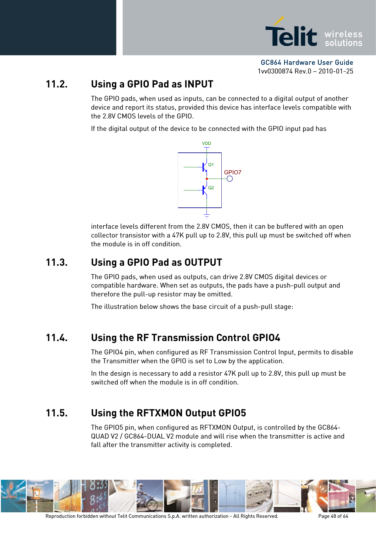
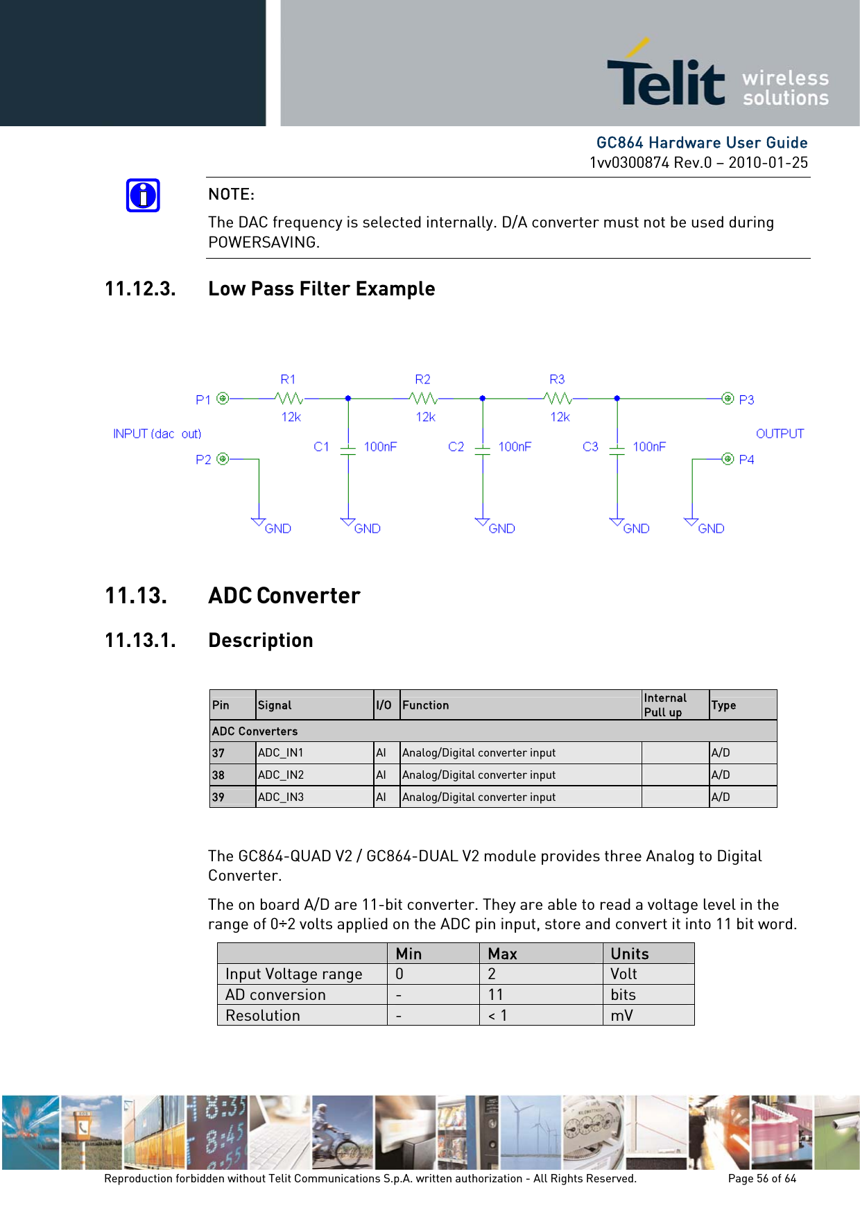
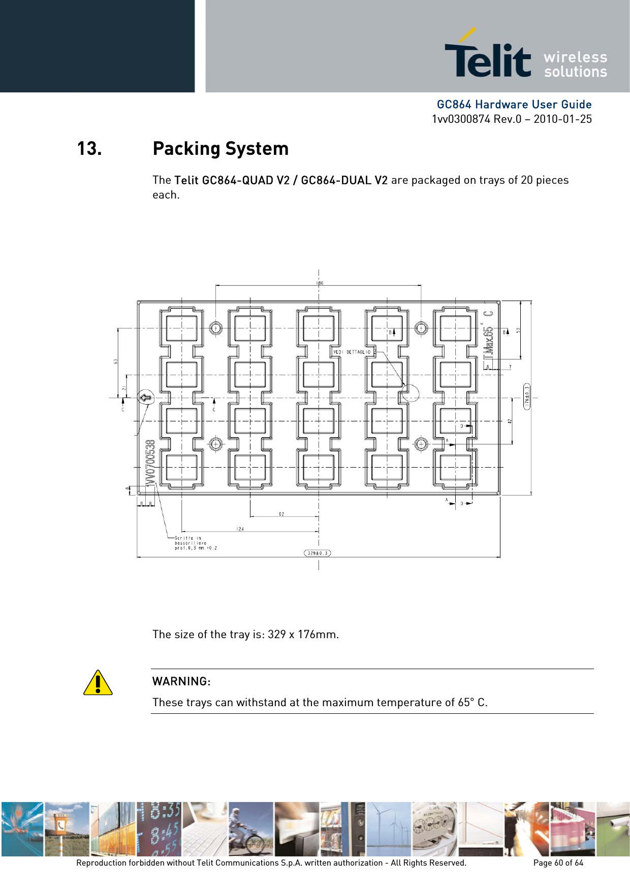
![GC864 Hardware User Guide 1vv0300874 Rev.0 – 2010-01-25 Reproduction forbidden without Telit Communications S.p.A. written authorization - All Rights Reserved. Page 55 of 64 11.12. DAC Converter 11.12.1. Description Pin Signal I/O Function Internal Pull up Type DAC Converter 40 DAC_OUT AO Digital/Analog converter output D/A The GC864-QUAD V2 / GC864-DUAL V2 module provides one Digital to Analog Converter. The on board DAC is a 10-bit converter, able to generate a analogue value based a specific input in the range from 0 up to 1023. However, an external low-pass filter is necessary. Min Max Units Voltage range (filtered) 0 2,6 Volt Range 0 1023 Steps The precision is 10 bits, so if we consider that the maximum voltage is 2V, the integrated voltage could be calculated with the following formula: Integrated output voltage = 2 * value / 1023 DAC_OUT line must be integrated (for example with a low band pass filter) in order to obtain an analog voltage. 11.12.2. Enabling DAC The AT command below is available to use the DAC function: AT#DAC[=<enable>[,<value>]] <value> – scale factor of the integrated output voltage (0–1023, with 10 bit precision), and it must be present if <enable>=1. Refer to SW User Guide or AT Commands Reference Guide for the full description of this function. Refer to SW User Guide or AT Commands Reference Guide for the full description of this function.](https://usermanual.wiki/Telit-Communications-S-p-A/GC864Q2/User-Guide-1259662-Page-55.png)