Telit Communications S p A GE864 GSM 850/1900MHz Module User Manual Telit GE863 QUAD PY Hardware User Guide
Telit Communications S.p.A. GSM 850/1900MHz Module Telit GE863 QUAD PY Hardware User Guide
Contents
- 1. Users Manual
- 2. user manual
Users Manual

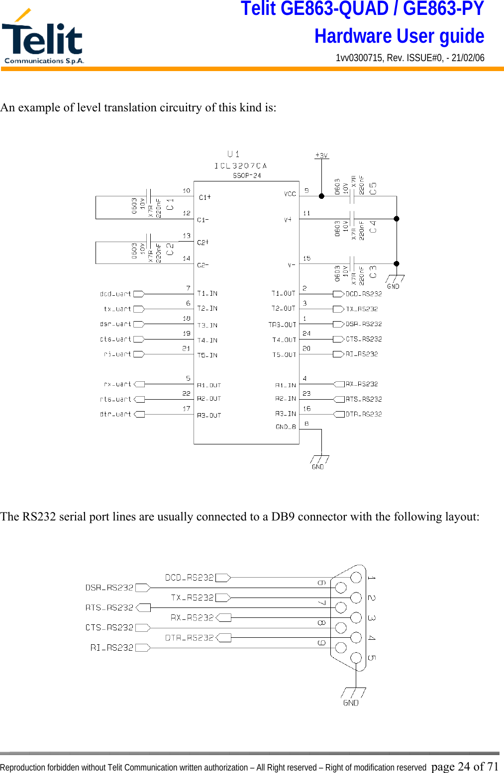
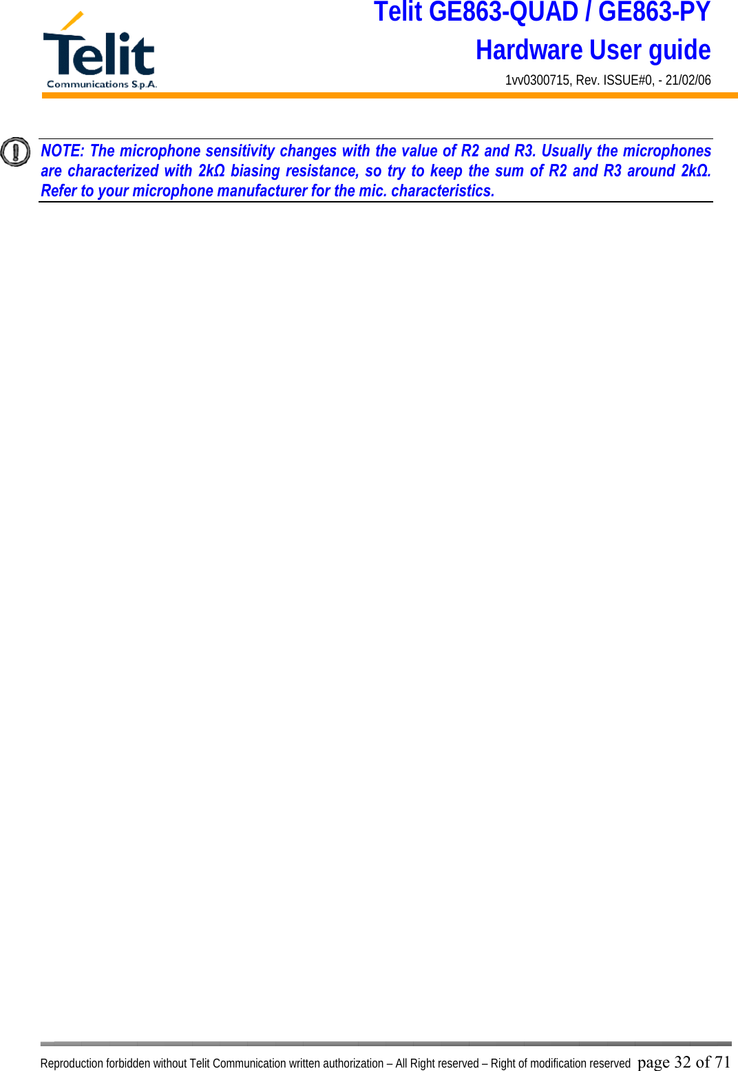
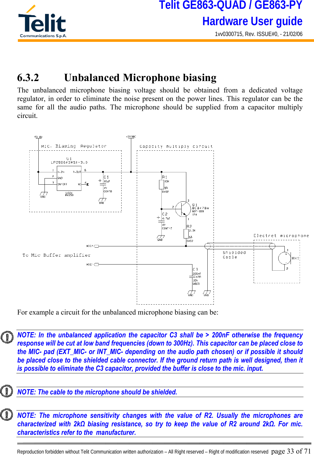
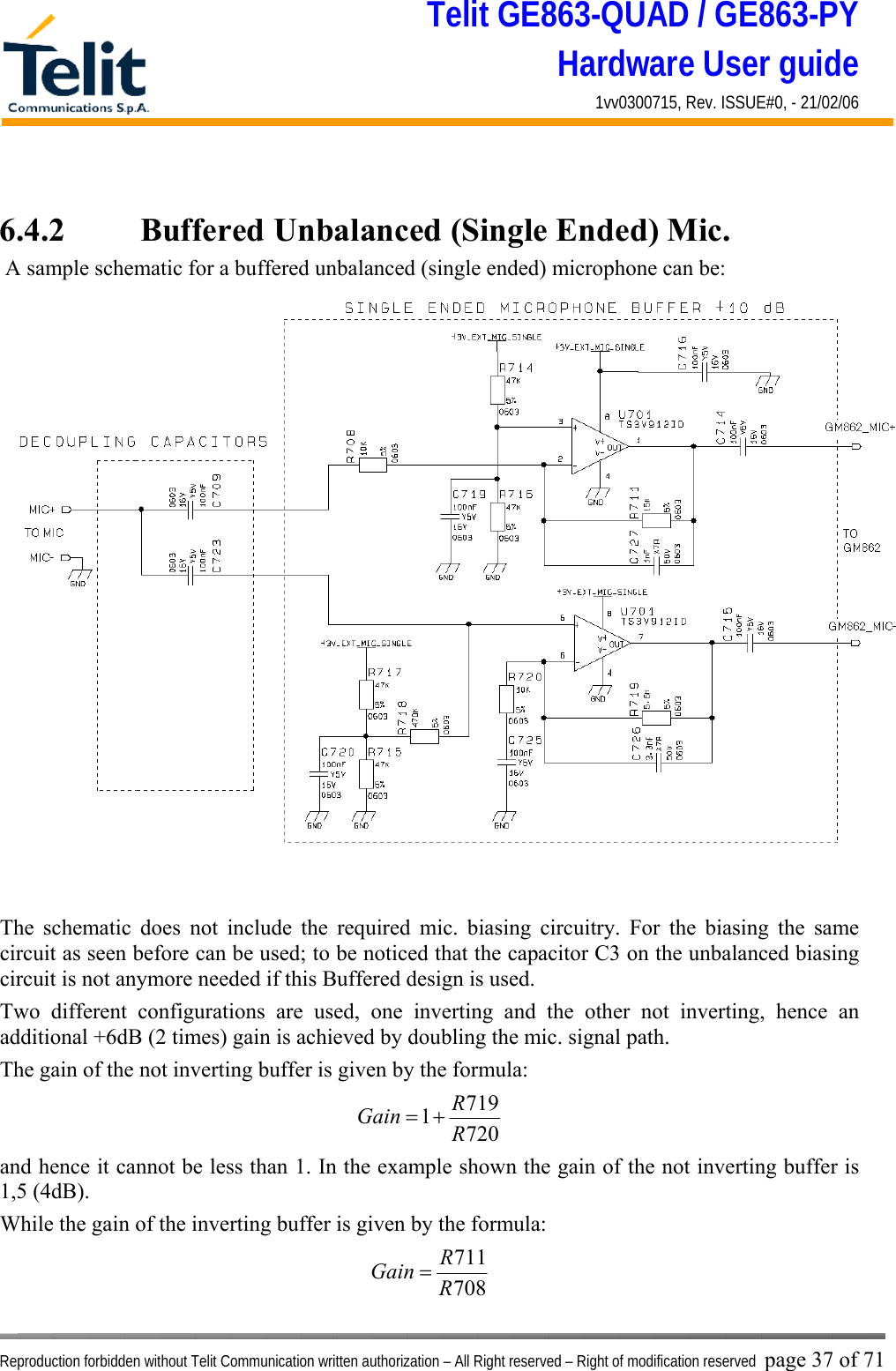
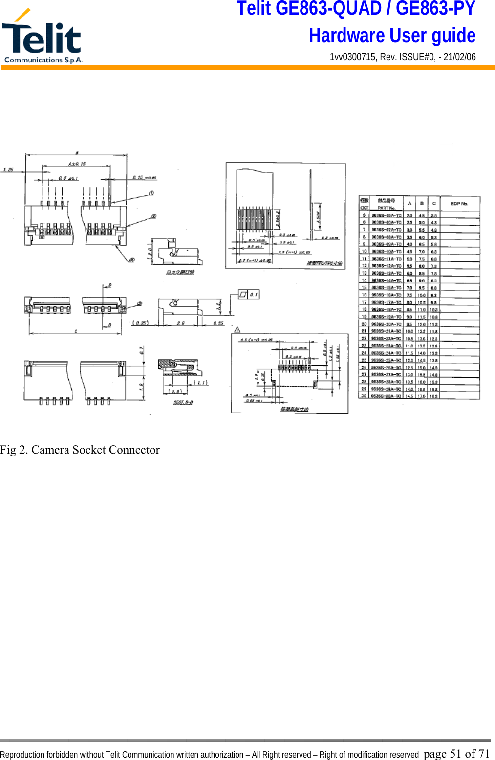
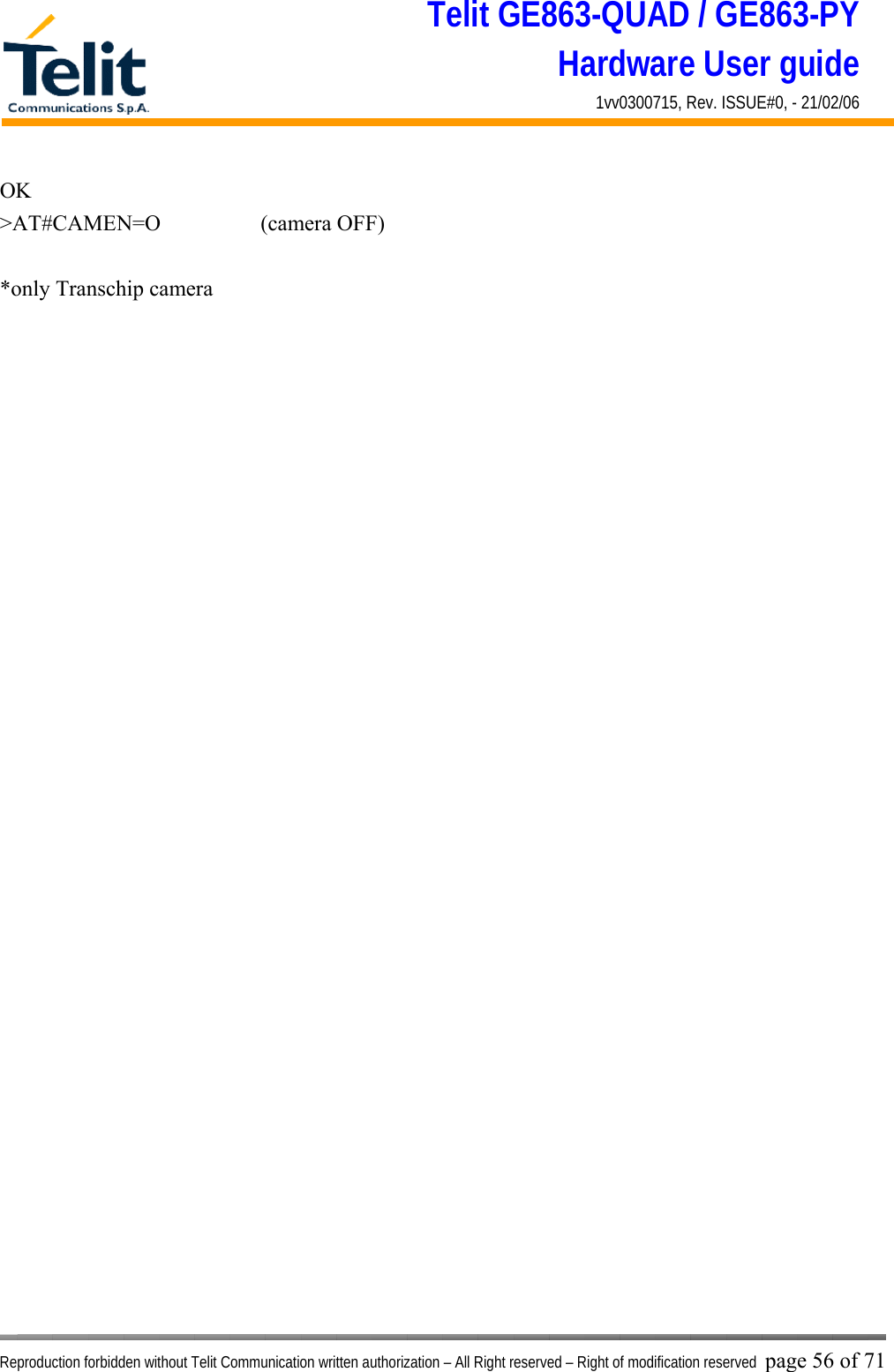
![Telit GE863-QUAD / GE863-PY Hardware User guide 1vv0300715, Rev. ISSUE#0, - 21/02/06 Reproduction forbidden without Telit Communication written authorization – All Right reserved – Right of modification reserved page 35 of 71 607606605604RRRRGain == The C636 and C637 capacitors are placed in order to cut off the gain at higher frequencies than the transmitted GSM band, the cutoff frequency (-3dB) should be 8 kHz in order to have -1dB at 4kHz. The cutoff frequency is given by the formula: 636*606*21637*604*21.CRCRfreqππ== [Hz] For example: - Let's assume you have a microphone with these characteristics: - sensitivity -45 dBVrms/Pa and you want to use it in the internal mic. audio path. With the mic. having nominal sensitivity -45dBVrms/Pa at the "normal spoken" conditions: -4.7dB Pa at 7 cm from the mouth of the talker. At that acoustic pressure the voltage output from the microphone is: Mic Voltage Output (dB) = ( -45) + (-4.7) = -49.7 dBVrms corresponding to: Mic_Voltage_Output = 10 ( -49.7 / 20 ) = 3.3* 10 -3 Vrms in order to have a signal of 50 mVrms on the GE863-QUAD/PY internal mic. inputs then the buffer must have a gain of: Voltage @ GE863-QUAD/PY_intmic/ Mic_Voltage_Output = (50 * 10 -3 )/( 3.3 * 10 -3 ) = 15 Hence in these conditions the signal level on the input pads of the internal mic. of the GE863-QUAD/PY is 24 dB (15 times) higher than the microphone output and therefore the buffer has to gain 24 dB. The corresponding values for the resistors on the buffer could be ( if we keep the input resistance 10kΩ ) R604 = R606 = gain* R603= gain* R605 = 15* 10 = 150 kΩ The commercial values of 150kΩ & 10kΩ are then chosen.](https://usermanual.wiki/Telit-Communications-S-p-A/GE864.Users-Manual/User-Guide-680636-Page-35.png)
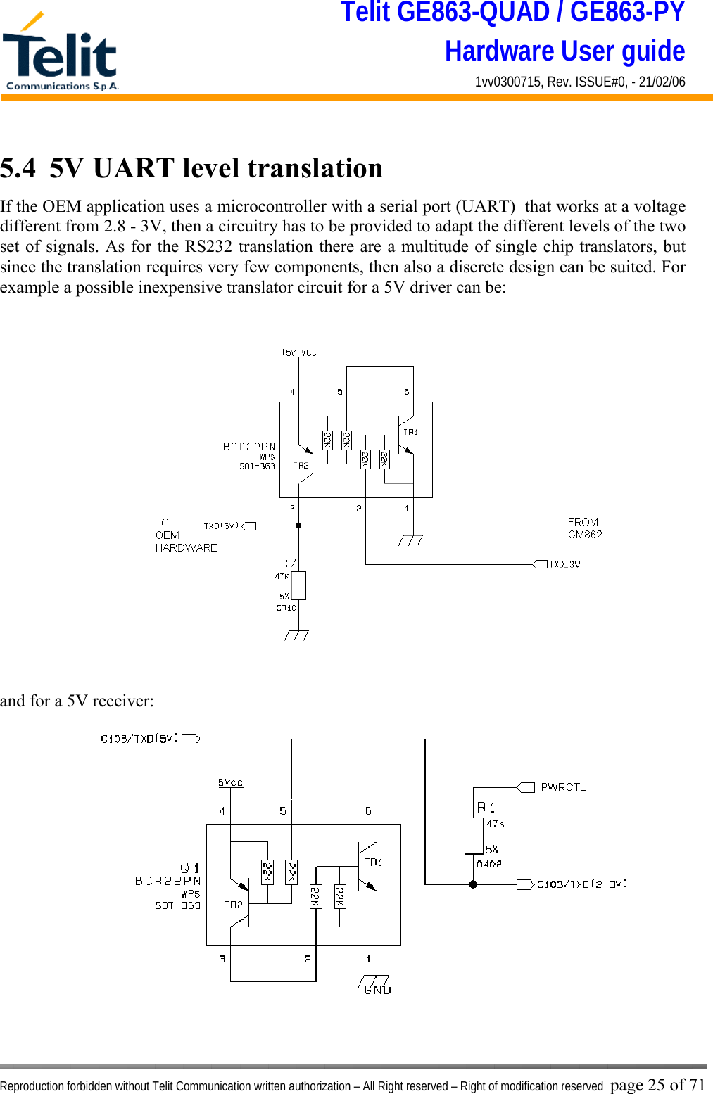
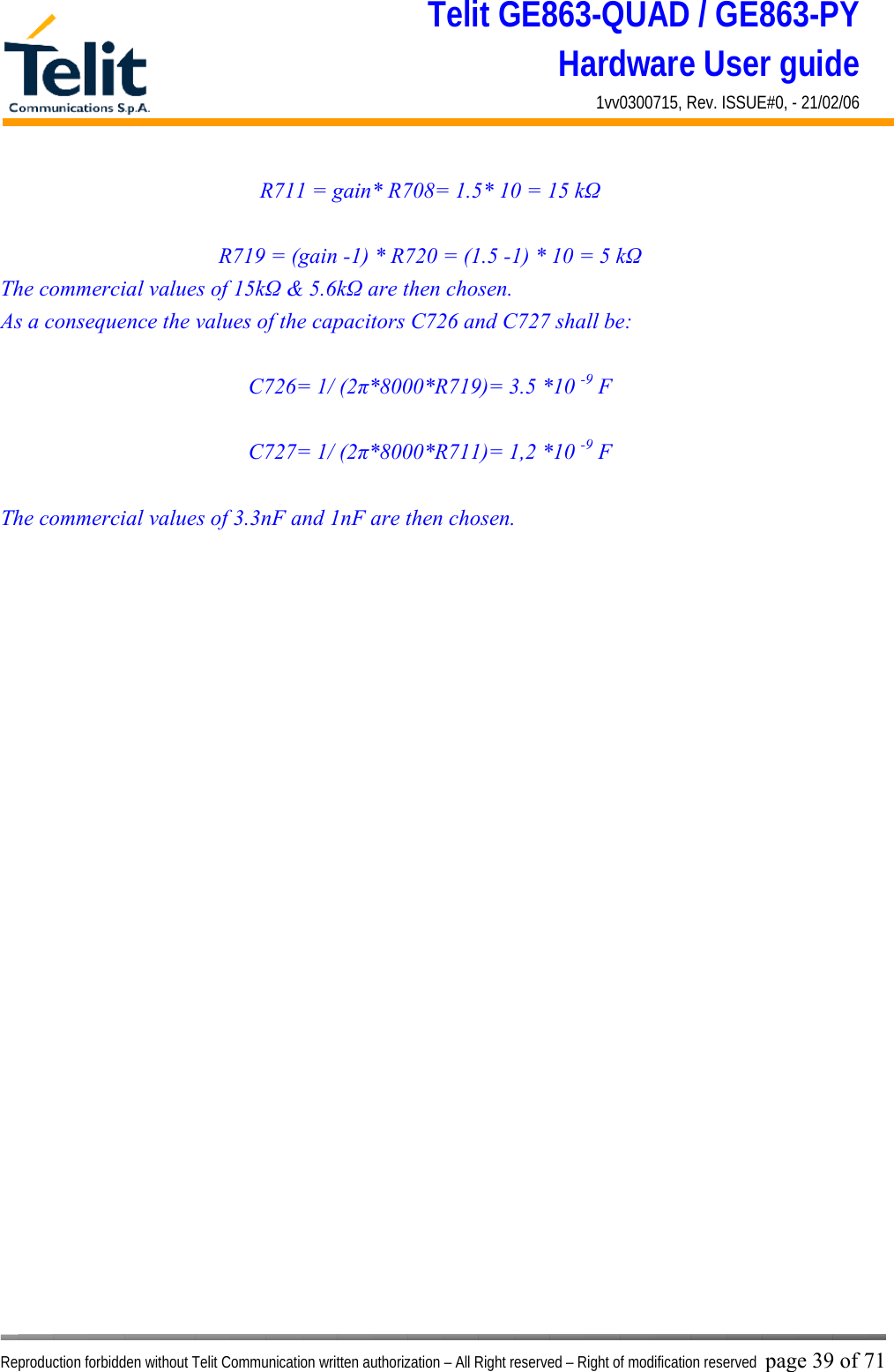
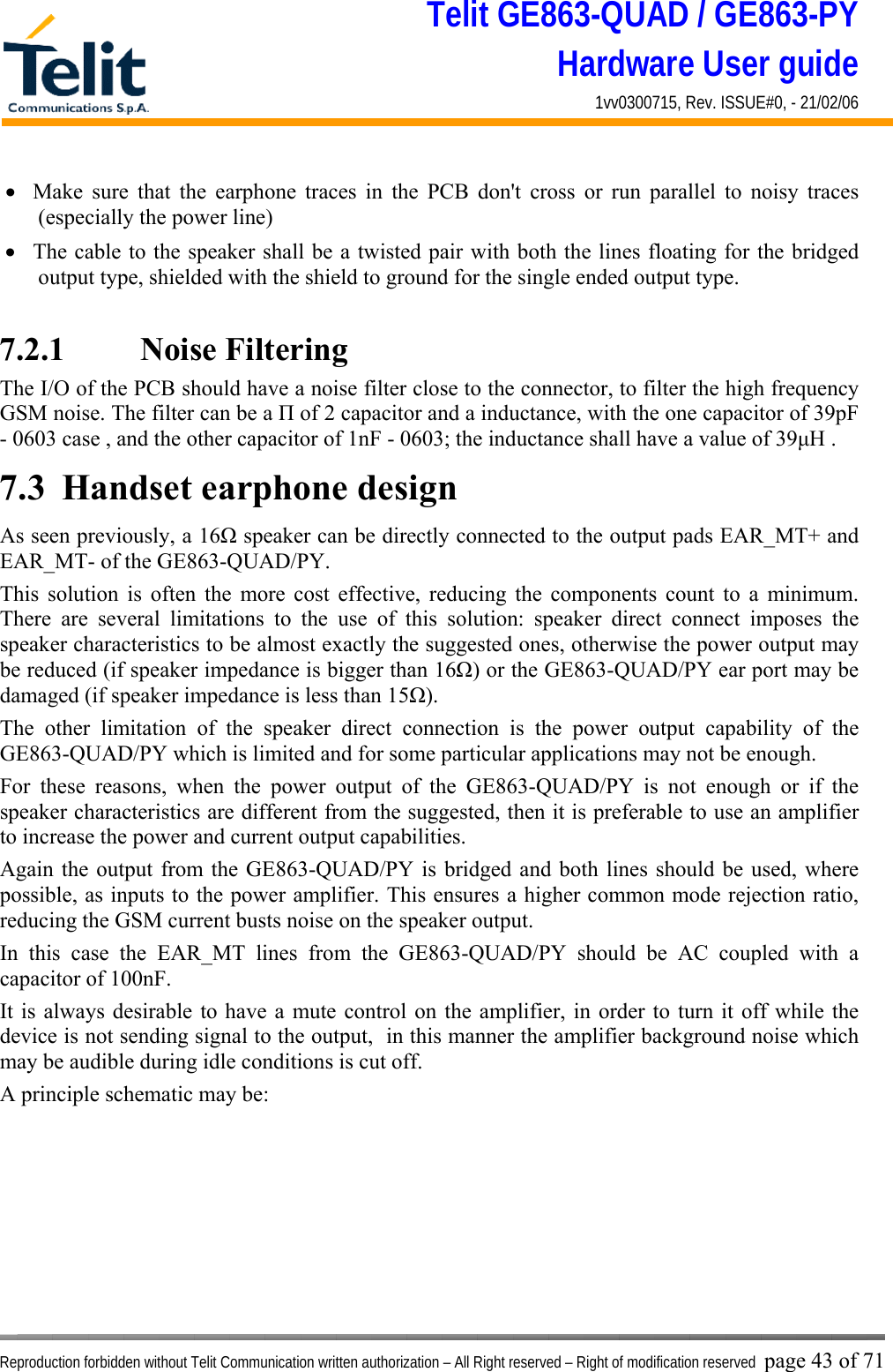
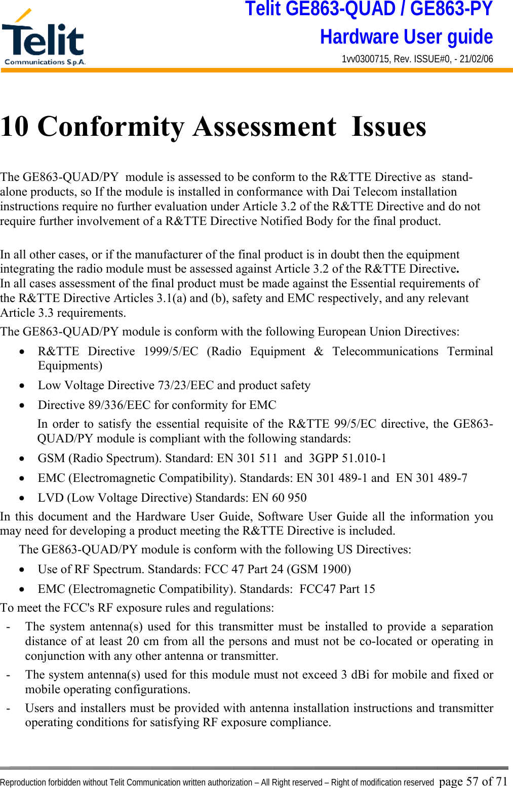
![Telit GE863-QUAD / GE863-PY Hardware User guide 1vv0300715, Rev. ISSUE#0, - 21/02/06 Reproduction forbidden without Telit Communication written authorization – All Right reserved – Right of modification reserved page 38 of 71 As shown in the balanced buffered mic. the gain adjustments can be done by changing R719 - R720 and R708 - R711 and as a consequence the capacitors C726 and C727. The bandwidth (-3dB) is given by the approximated formula (considering C725 >> C726) : 727*711*21726*719*21.CRCRfreqππ== [Hz] The buffer bandwidth at -3dB shall be 8kHz. Note that the biasing of the operational amplifier is given for the inverting amplifier by the series divider R714-R715. The 100nF capacitor C719 is needed to filter the noise that could be coupled to that divider. For the not inverting operational the biasing is given by a different divider R715-R717 with the capacitor C720 and through a series resistor R718 of 470KΩ. For example: - Let's assume you have a microphone with these characteristics: - sensitivity -45 dBVrms/Pa and you want to use it in the external mic. audio path. With the mic. having nominal sensitivity -45dBVrms/Pa at the "normal spoken" conditions: -4.7dB Pa but at 50 cm from the mouth of the talker an additional 20 dB loss shall be considered. At that acoustic pressure the voltage output from the microphone is: Mic Voltage Output (dB) = ( -45) + (-4.7) -20 = -69.7 dBVrms corresponding to: Mic_Voltage_Output = 10 ( -69.7 / 20 ) = 3.3* 10 -4 Vrms in order to have a signal of 1 mVrms (10 dB lower than the nominal input for the GE863-QUAD/PY external mic. path) on the GE863-QUAD/PY internal mic. inputs then the buffer must have a gain of: Voltage @ GE863-QUAD/PY_intmic/ Mic_Voltage_Output = (1 * 10 -3 )/( 3.3 * 10 -4 ) = 3 Hence in these conditions the signal level on the input pads of the internal mic. of the GE863-QUAD/PY is 10 dB (3 times) higher than the microphone output and therefore the buffer has to gain 10 dB. To calculate the resistor values it must be kept in mind that balancing the line will double the signal and hence already add +6 dB, therefore the buffer must gain only 1.5 times. The corresponding values for the resistors on the buffer could be ( if we keep the input resistance 10kΩ )](https://usermanual.wiki/Telit-Communications-S-p-A/GE864.Users-Manual/User-Guide-680636-Page-38.png)
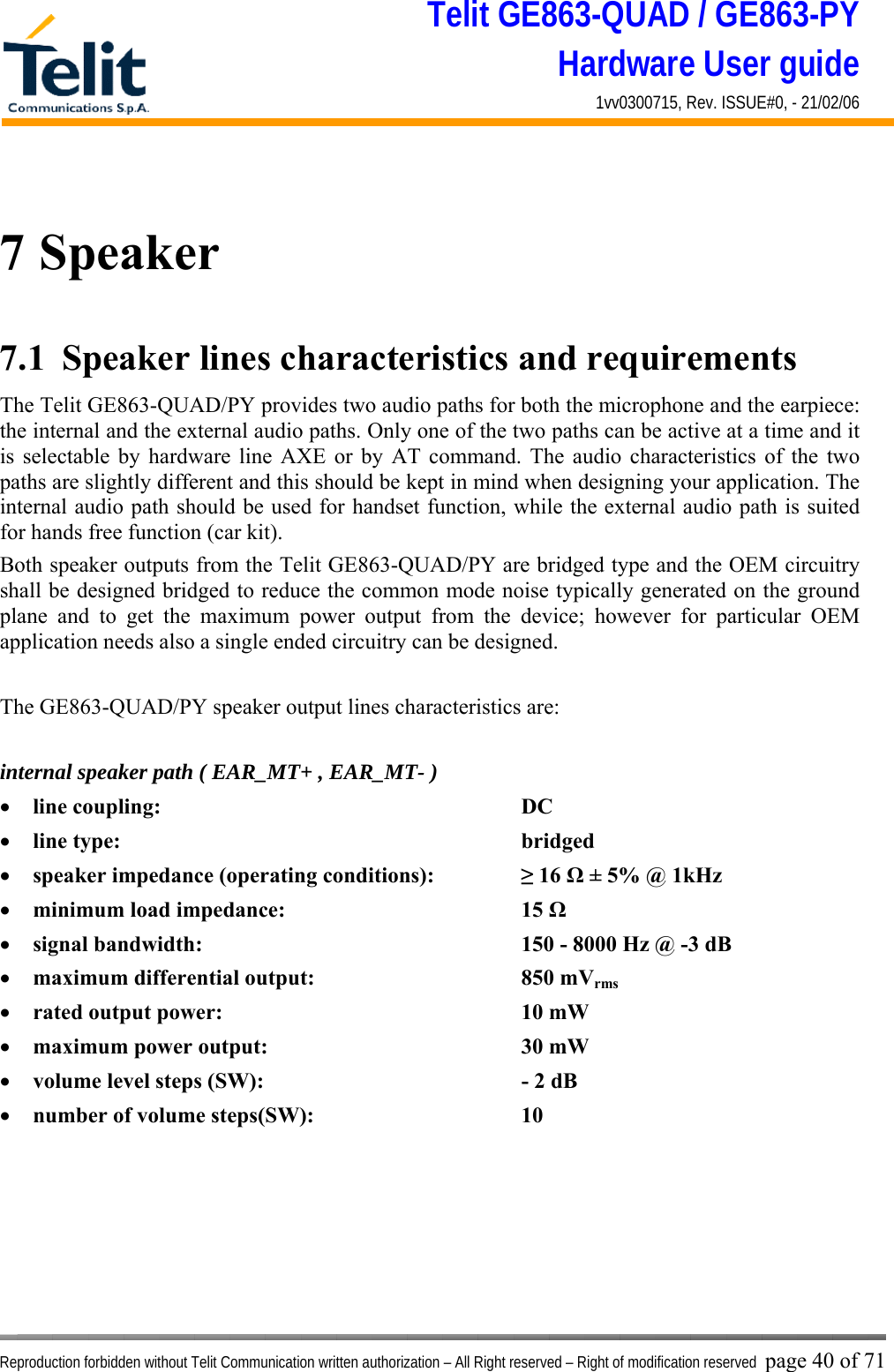
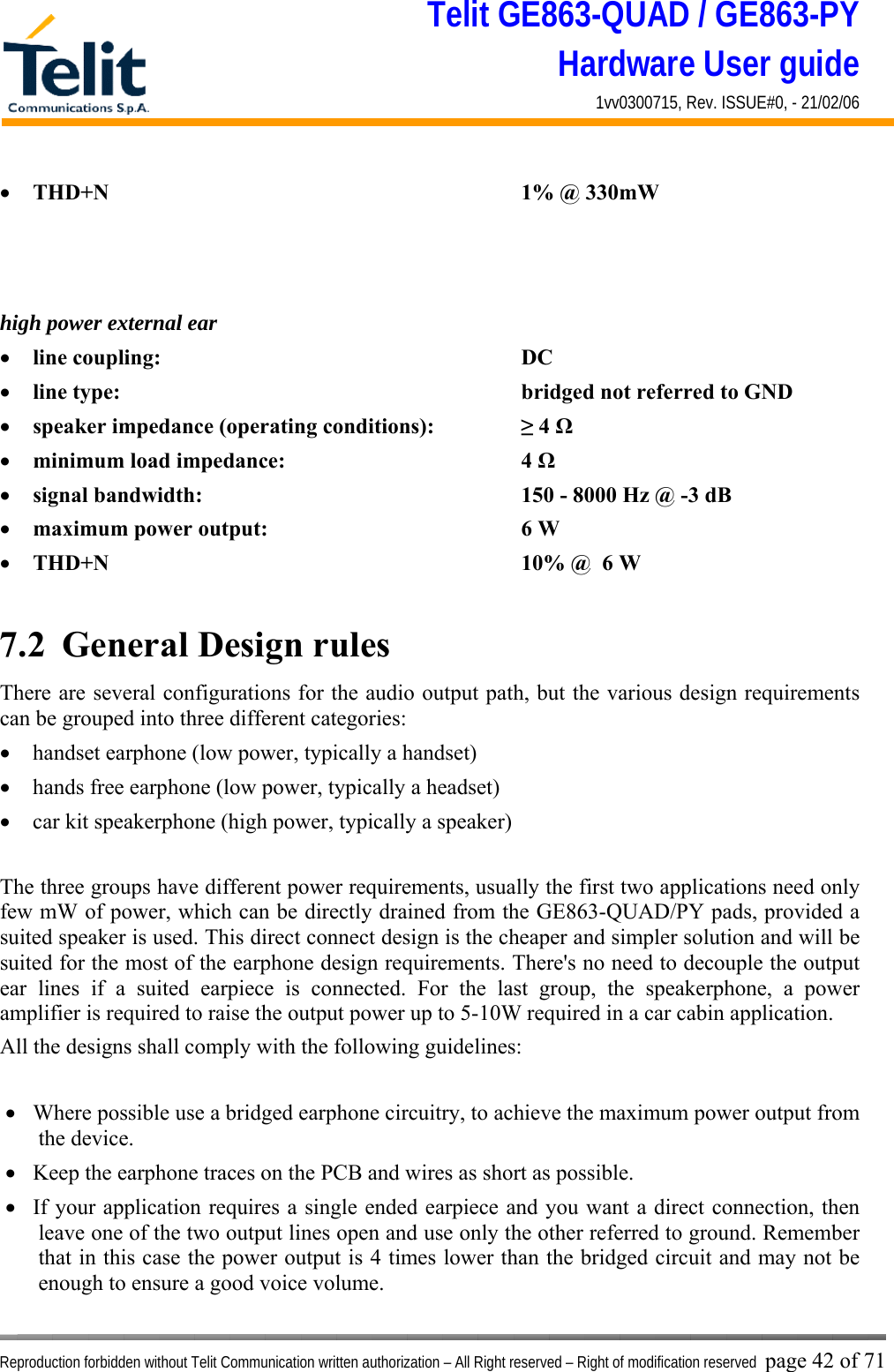
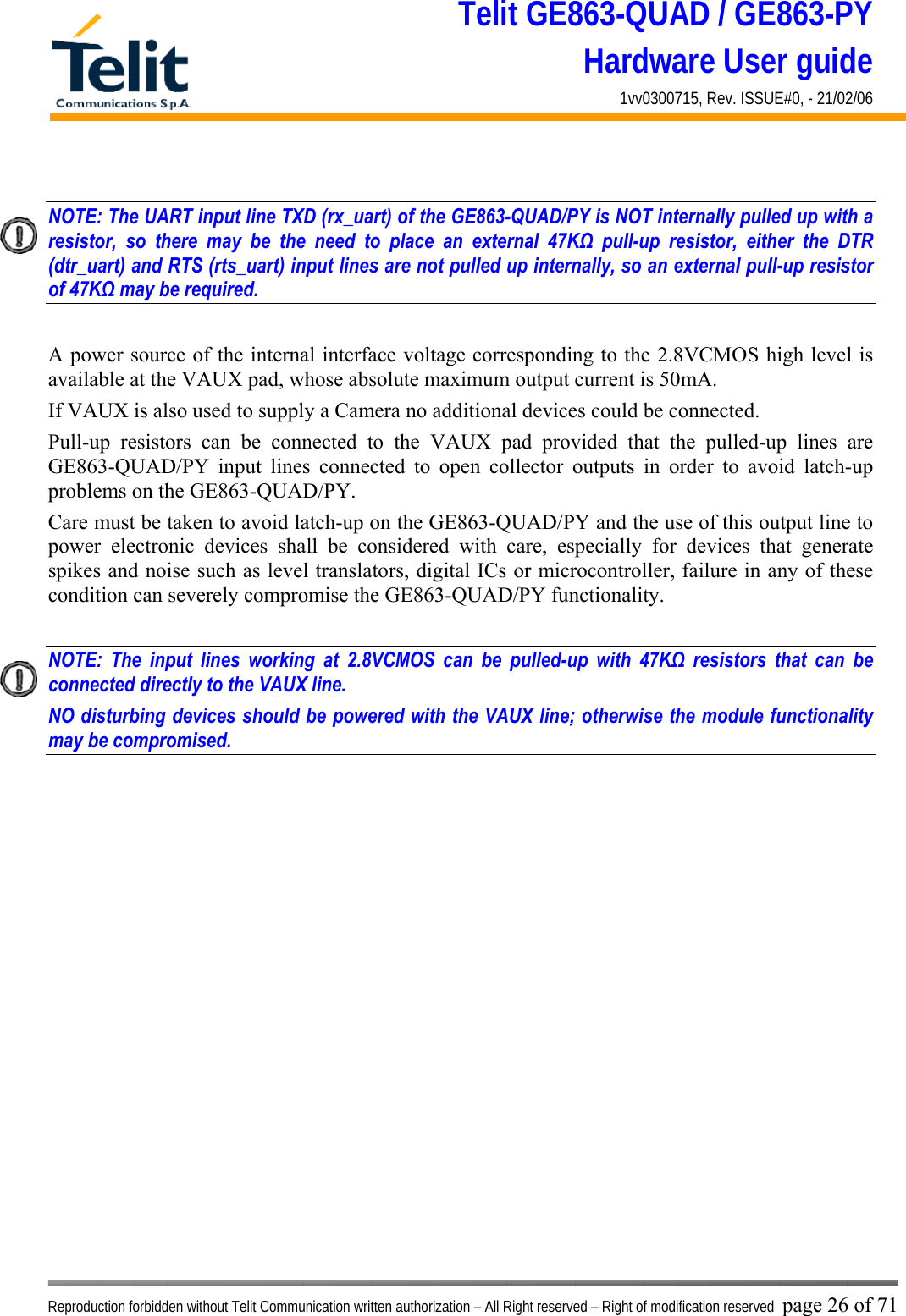
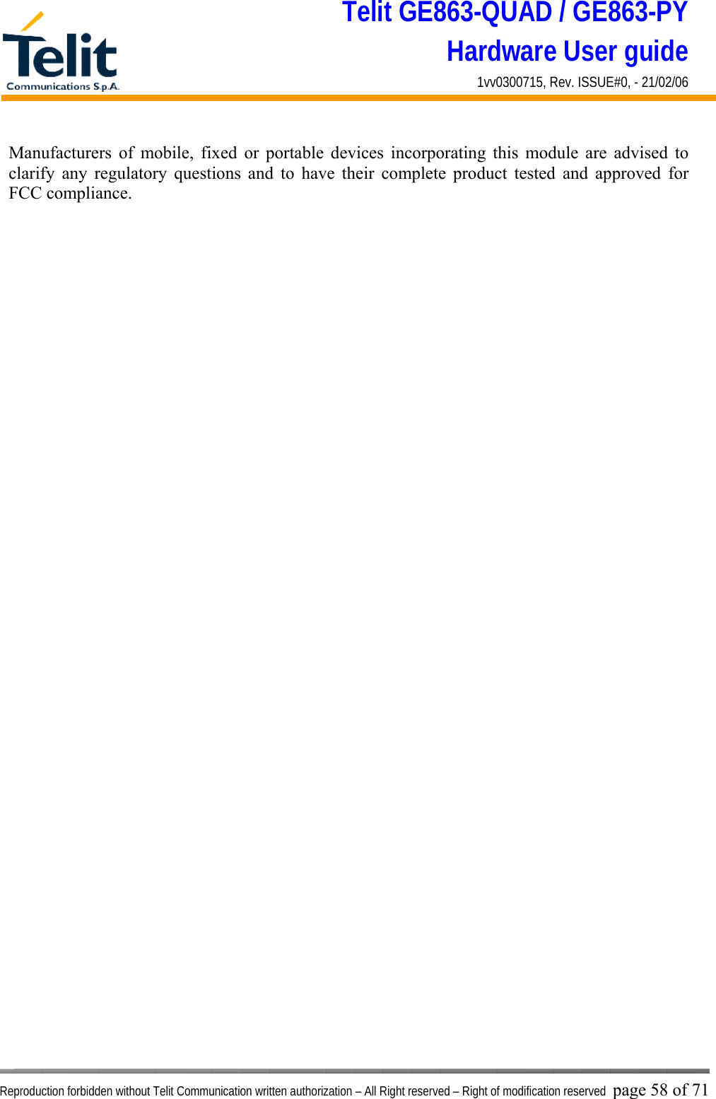
![Telit GE863-QUAD / GE863-PY Hardware User guide 1vv0300715, Rev. ISSUE#0, - 21/02/06 Reproduction forbidden without Telit Communication written authorization – All Right reserved – Right of modification reserved page 44 of 71 The resulting gain and high pass cut can be obtained with the formula: 23RRGain = 4*3*21.CRfreqπ= [Hz] And an example of internal Ear amplifier is:](https://usermanual.wiki/Telit-Communications-S-p-A/GE864.Users-Manual/User-Guide-680636-Page-44.png)
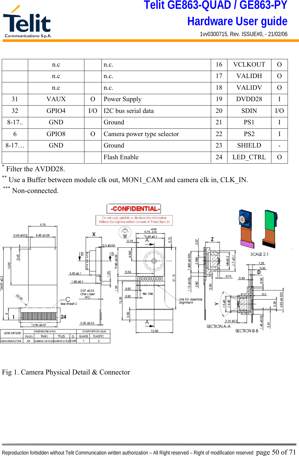
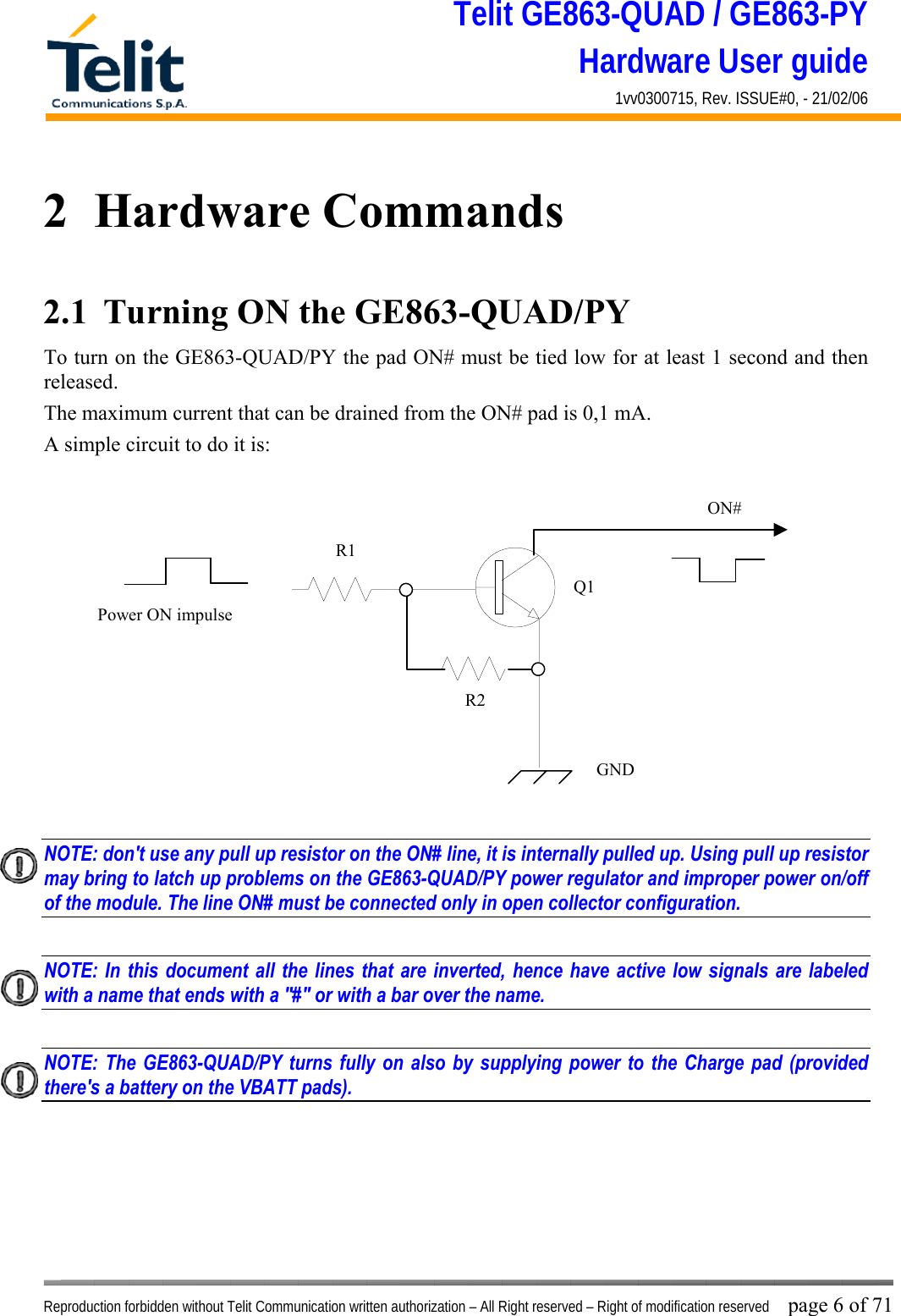
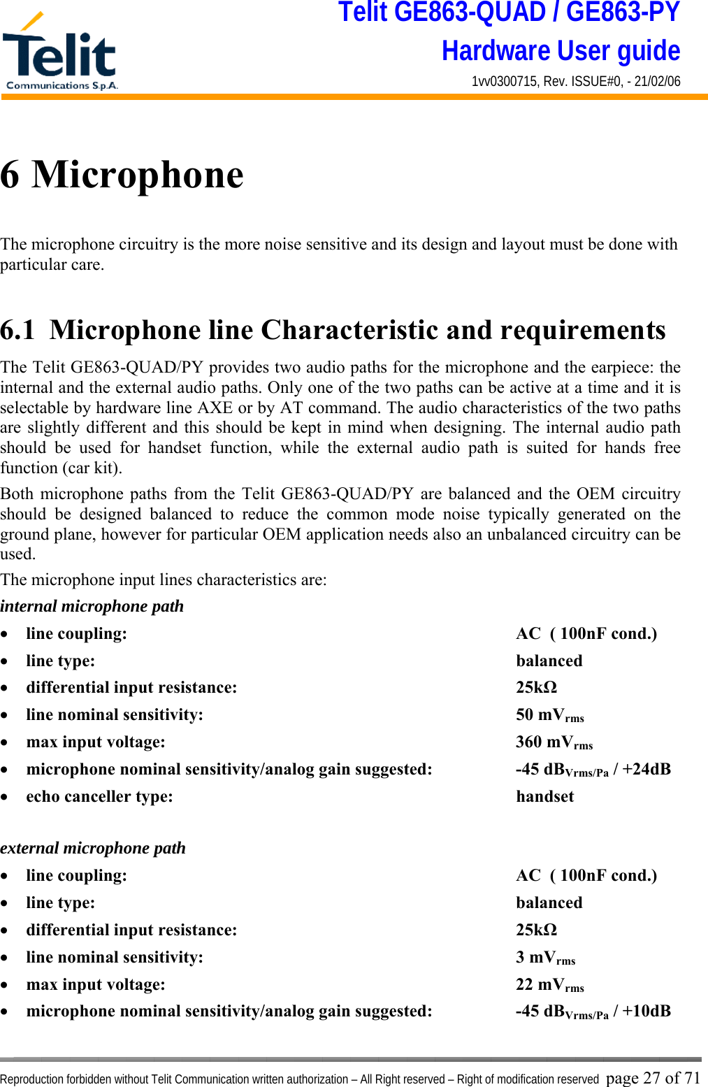
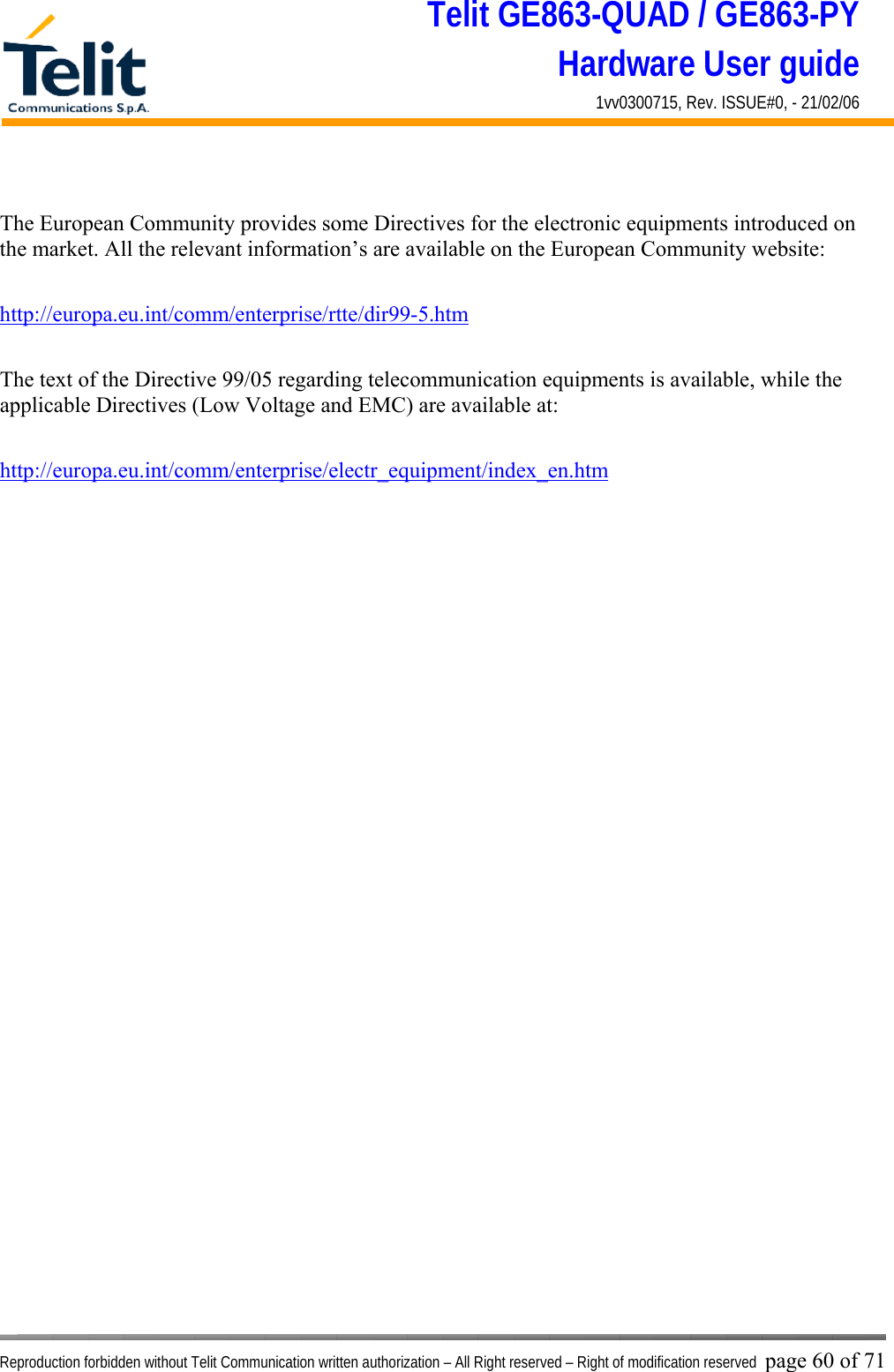
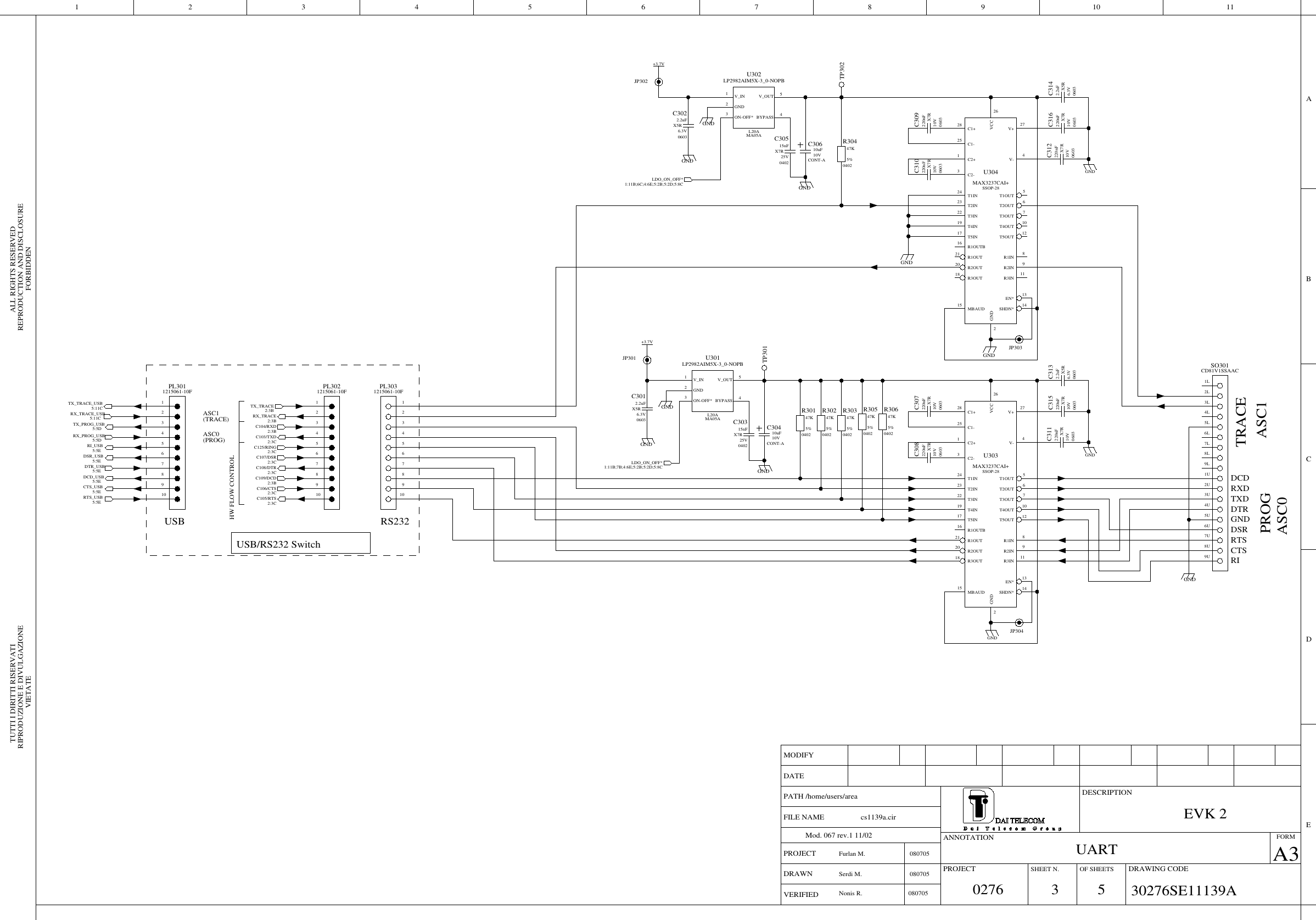
![Telit GE863-QUAD / GE863-PY Hardware User guide 1vv0300715, Rev. ISSUE#0, - 21/02/06 Reproduction forbidden without Telit Communication written authorization – All Right reserved – Right of modification reserved page 53 of 71 9.1.3 Block Diagram for supported cameras The numbers on the left side of the Camera’s connectors refers to Module Connector’s pin number. DVDD is VAUX1 power supply from GE863-QUAD/PY 1 2 3 4 5 6 7 8 9 10 11 12 13 14 15 16 17 18 19 20 21 22 23 24 GNDAVDDCAM_CLKGNDDVDDIICSDA_CAMGNDGNDPD[1]PD[0]PD[6]CAM_CLKDVDD AVDDGND CAMERA TRANSCHIP MON1_CAM](https://usermanual.wiki/Telit-Communications-S-p-A/GE864.Users-Manual/User-Guide-680636-Page-53.png)

![040247K5%noMount=YESR111L18ALP2982AIM5X–2_8–NOPBMA05AU1021V_IN3ON–OFF4BYPASS5V_OUT2GNDIICSCL/AGILENT6BCAM_SCL/IIC_SCL9BCAM_M_CLK10D;5ACAM_M_CLK5A;5CCAM_SDA/IIC_SDA5D;6BTP101TP106GNDVAUX1TP105GND04021K5%R104GNDTP108VAUX1TP110040200noMount=YESR113GNDGNDGNDJP11625V040215nFX7RnoMount=YESC106JP120JP10910VCONT–A10uFC104FORBIDDENVIETATEALL RIGHTS RESERVEDRIPRODUZIONE E DIVULGAZIONE REPRODUCTION AND DISCLOSURETUTTI I DIRITTI RISERVATIPROJECTA3DESCRIPTIONDRAWING CODEFORMMODIFYOF SHEETSDATESHEET N.VERIFIEDPROJECTDRAWNPATH /home/users/areaMod. 067 rev.1 11/02 ANNOTATIONFILE NAMEBCDEA42 98 1071 3 1165040247K5%noMount=YESR110VCC_MAIN_CAM6.3V06032.2uFX5RC109CAM_DRDY/AGILENT6BPD[5]5A4773540103470SO107213PD[1]5AJP106JP107GNDGNDGNDTP109040200R115040200R112PD[0]5APD[2]5A040200R10610V0402100nFY5VC1126BCAM_PWR_ON/AGILENTVCC_MAIN_CAMSN74LVC1G08DCKRU1015VCC3GNDTGPIO_08/CAM_ON9BPD[4]5AJP114040200R105CAM_SYNC/AGILENT5AMON1/CAM_CLK10DPD[3]5APD[6]5AVCC_MAIN_CAMCAM_SDA/IIC_SDA6B;9B4773540103470SO109213TP10225V040215nFX7RC10525V040215nFX7RnoMount=YESC111TGPIO_08/CAM_ON5D040200R109noMount=YES52437–2472SO105321456789101112131415161718192021222324CAM_SCL/IIC_SCL5CTP1114773540103470SO106213TP107TGPIO_09/CAM_RST5COT101JP105JP1174779723130417SO102321456789101112131415161718192021222324252627282930040200R114SN74LVC1G08DCKRCEU101241040200R116040200R1084779723130417SO101321456789101112131415161718192021222324252627282930TP1046.3V06032.2uFX5RC11050V040233pFCOGC107GNDPD[7]5BCAM_PWR_ON/AGILENT6B6.3V06032.2uFX5RC108GNDJP108TGPIO_09/CAM_RST9B040200R1070402100K5%R103GNDGNDJP112TP112TP103JP1214773540102470noMount=YESSO10421JP110GND4773540103470SO108213MON1/CAM_CLK9B10276Furlan M. 0609051 30276SE11170Pasqualini N.cs1170.cir I2CBUS DUAL CAMERA060905SCLKRESET_NDVDD28ShieldSDINPS1VALIDHAVDD28VCLKOUTLED_CTRLTransChip TC5747MF24L (24pin)VALIDVPS2AGNDDGNDCLK_ININTERFACE CONNECTORSTC5747MF24LDOUT1DOUT3DOUT2DOUT0DOUT6DOUT4DOUT5DOUT7DOUT8GM862TRIZIUM– 1 –](https://usermanual.wiki/Telit-Communications-S-p-A/GE864.Users-Manual/User-Guide-680636-Page-69.png)