Telit Communications S p A GE910G Quad band GSM/GPRS module User Manual 1vv0300962 GE910 Hardware User Guide r9 bis3
Telit Communications S.p.A. Quad band GSM/GPRS module 1vv0300962 GE910 Hardware User Guide r9 bis3
Contents
- 1. User manual revised
- 2. User manual
User manual revised

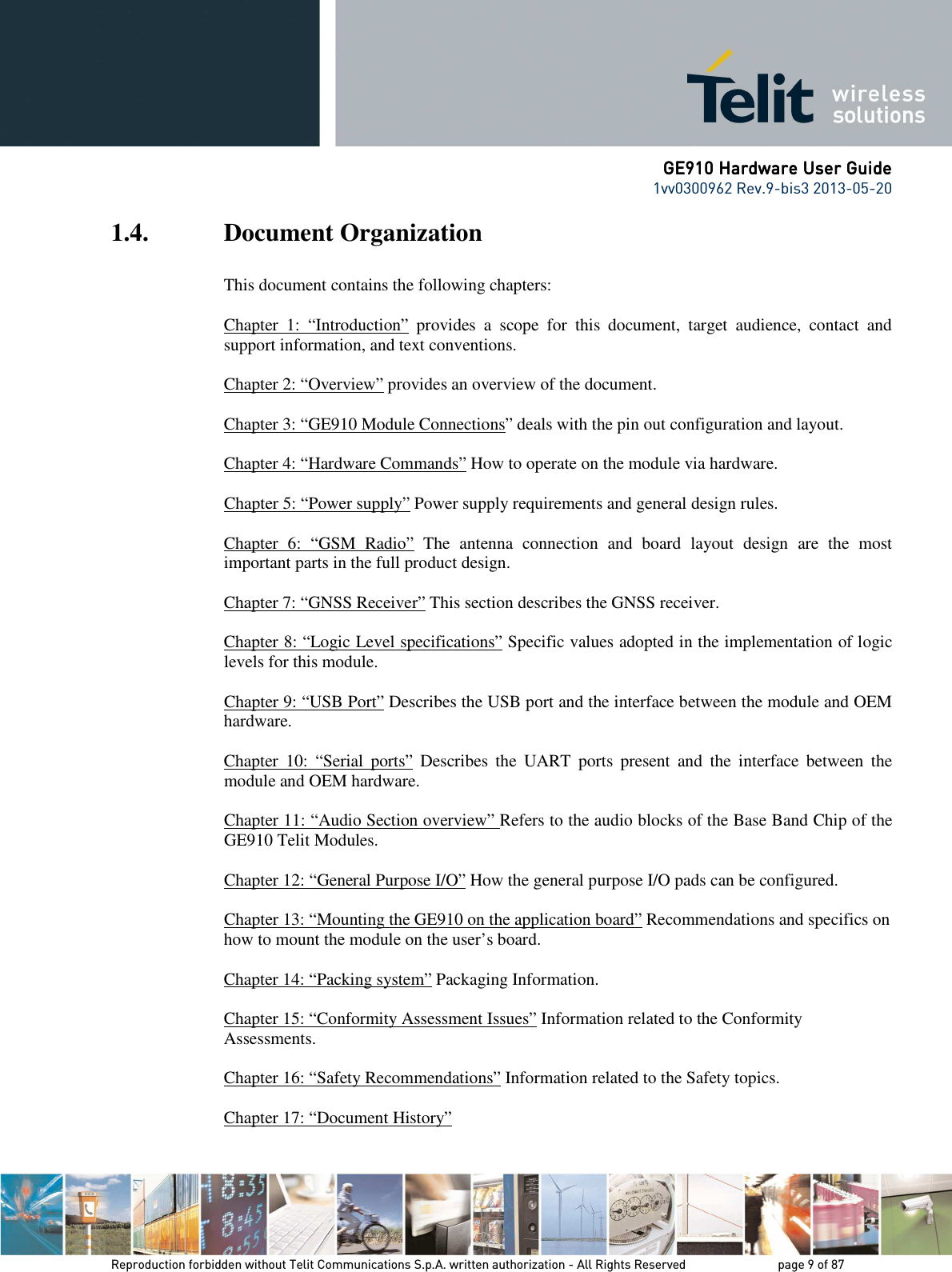


![GE910 Hardware User GuideGE910 Hardware User GuideGE910 Hardware User GuideGE910 Hardware User Guide 1vv0300962 Rev.9-bis3 2013-05-20 Reproduction forbidden without Telit Communications S.p.A. written authorization - All Rights Reserved page 50 of 87 Mod. 0805 2011-07 Rev.2 7.4.10. External LNA Enable The GE910 is already provided by an internal LNA. In case the Application needs to include an additional LNA stage, the module is provided by a digital signal usable to enable the power supply of the external amplifier. The signal is set to High only when the GPS receiver is active. The electrical characteristics of the GPS_LNA_EN signal are: Level Min [V] Max [V] Output High Level 1.6 1.9 Output Low Level 0V 0.2 Example of external antenna bias circuitry:](https://usermanual.wiki/Telit-Communications-S-p-A/GE910G.User-manual-revised/User-Guide-1968260-Page-50.png)
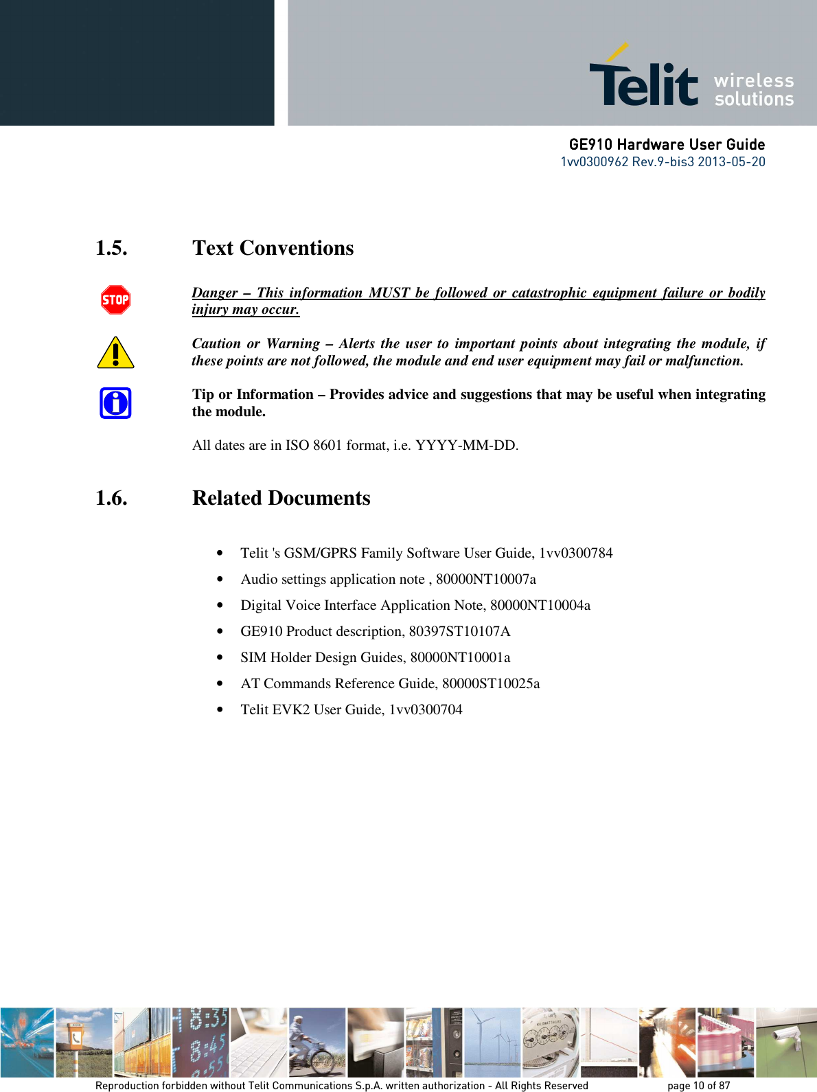
![GE910 Hardware User GuideGE910 Hardware User GuideGE910 Hardware User GuideGE910 Hardware User Guide 1vv0300962 Rev.9-bis3 2013-05-20 Reproduction forbidden without Telit Communications S.p.A. written authorization - All Rights Reserved page 72 of 87 Mod. 0805 2011-07 Rev.2 It is not recommended to place via or micro-via not covered by solder resist in an area of 0.3 mm around the pads unless it carries the same signal of the pad itself (see following figure). Holes in pad are allowed only for blind holes and not for through holes. When using the hole in pad, we suggest the via filling. Recommendations for PCB pad surfaces: Finish Layer thickness [µm] Properties Electro-less Ni / Immersion Au 3 –7 / 0.05 – 0.15 good solder ability protection, high shear force values The PCB must be able to resist the higher temperatures which are occurring at the lead-free process. This issue should be discussed with the PCB-supplier. Generally, the wettability of tin-lead solder paste on the described surface plating is better compared to lead-free solder paste. Inhibit area for micro-via](https://usermanual.wiki/Telit-Communications-S-p-A/GE910G.User-manual-revised/User-Guide-1968260-Page-72.png)