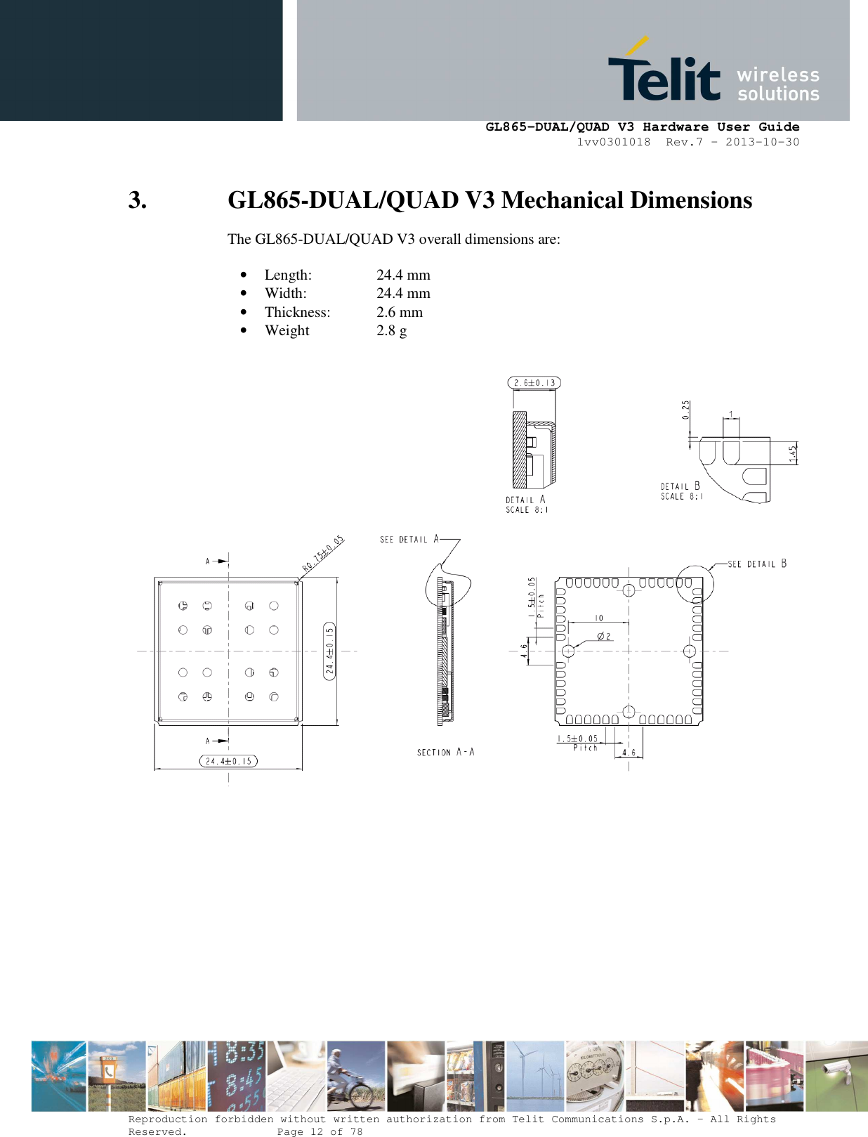
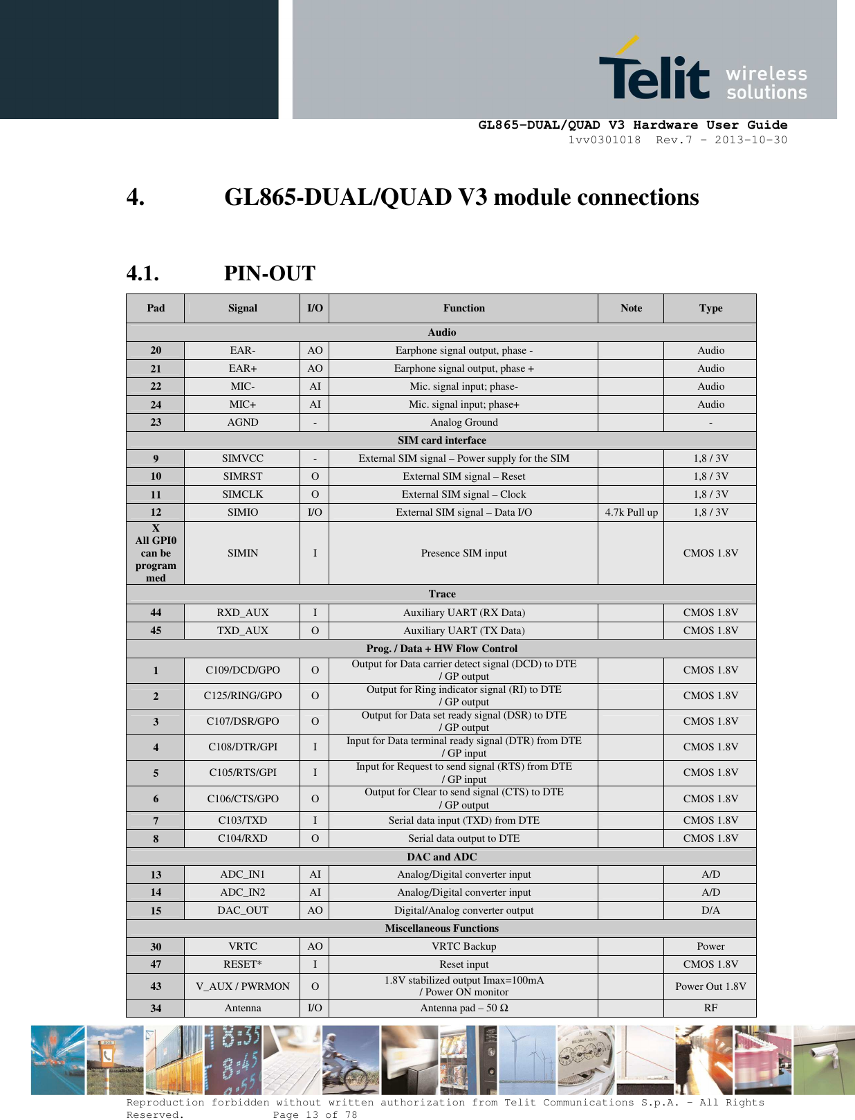
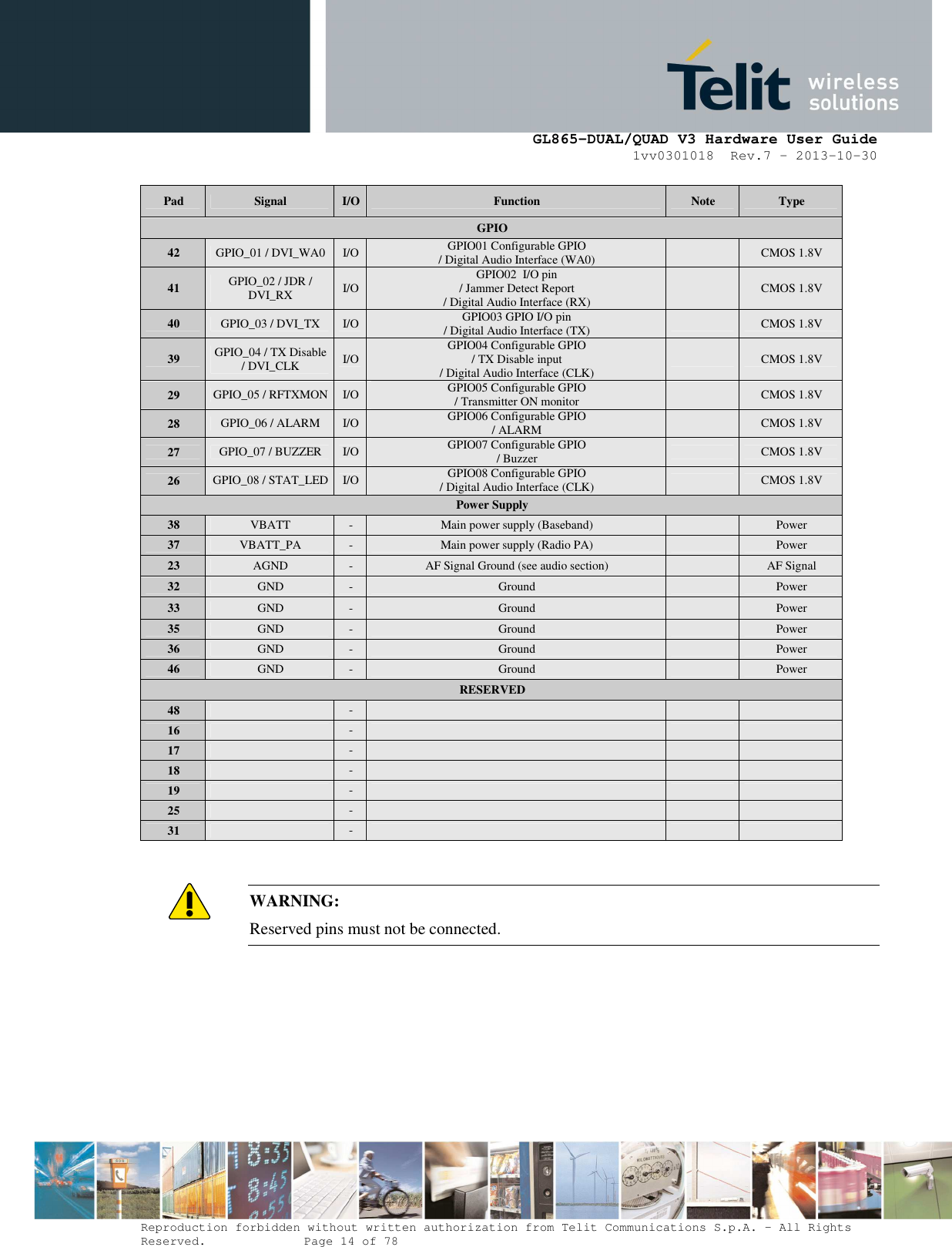
Telit Communications S p A GL865Q3 Quad Band GSM/GPRS module User Manual
Telit Communications S.p.A. Quad Band GSM/GPRS module
UserManual.wiki
>
Telit Communications S p A
>
GL865Q3 User Manual
User manual
Navigation menu
Upload a User Manual
Namespaces
Wiki Guide
HTML
PDF
Info
Views
User Manual
Discussion / Help
Navigation

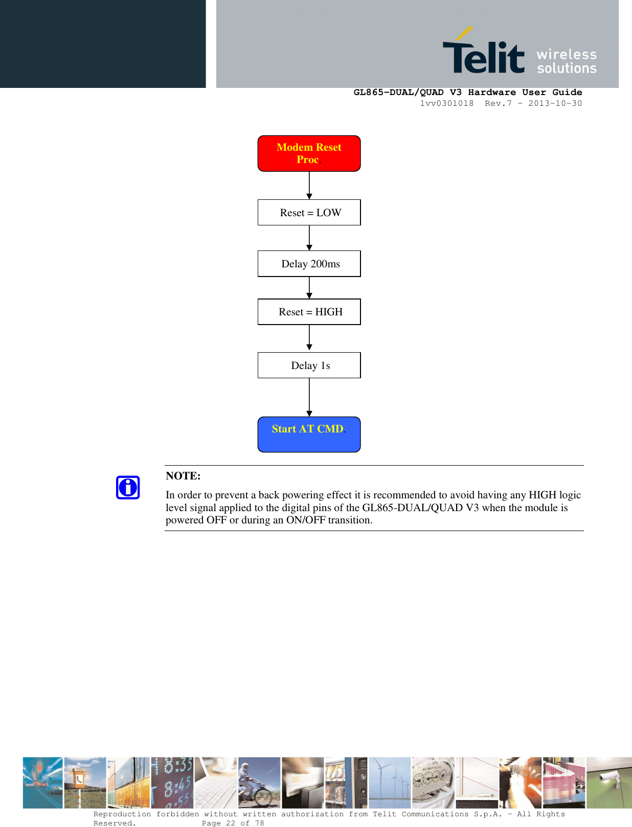
![GL865-DUAL/QUAD V3 Hardware User Guide 1vv0301018 Rev.7 – 2013-10-30 Reproduction forbidden without written authorization from Telit Communications S.p.A. - All Rights Reserved. Page 58 of 78 Mod. 0805 2011-07 Rev.2 12.1.2. Enabling DAC An AT command is available to use the DAC function. The command is: AT#DAC= [<enable> [, <value>]] <value> - scale factor of the integrated output voltage (0..1023 - 10 bit precision) it must be present if <enable>=1 Refer to SW User Guide or AT Commands Reference Guide for the full description of this function. NOTE: The DAC frequency is selected internally. D/A converter must not be used during POWERSAVING. 12.1.3. Low Pass Filter Example](https://usermanual.wiki/Telit-Communications-S-p-A/GL865Q3/User-Guide-2125318-Page-58.png)
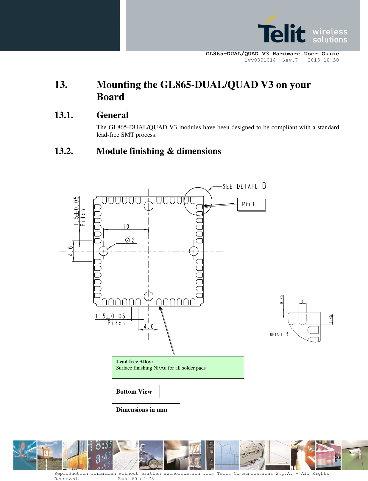
![GL865-DUAL/QUAD V3 Hardware User Guide 1vv0301018 Rev.7 – 2013-10-30 Reproduction forbidden without written authorization from Telit Communications S.p.A. - All Rights Reserved. Page 63 of 78 Mod. 0805 2011-07 Rev.2 Holes in pad are allowed only for blind holes and not for through holes. Recommendations for PCB pad surfaces: Finish Layer thickness [µm] Properties Electro-less Ni / Immersion Au 3 –7 / 0.05 – 0.15 good solder ability protection, high shear force values The PCB must be able to resist the higher temperatures which are occurring at the lead-free process. This issue should be discussed with the PCB-supplier. Generally, the wettability of tin-lead solder paste on the described surface plating is better compared to lead-free solder paste. It is not necessary to panel the application PCB, however in that case it is suggested to use milled contours and predrilled board breakouts; scoring or v-cut solutions are not recommended. Inhibit area for micro-via](https://usermanual.wiki/Telit-Communications-S-p-A/GL865Q3/User-Guide-2125318-Page-63.png)