Telit Communications S p A LE910C1NA Wireless Module User Manual LE910Cx HW User Guide
Telit Communications S.p.A. Wireless Module LE910Cx HW User Guide
UserManual.wiki
>
Telit Communications S p A
>
LE910C1NA User Manual
User guide
Navigation menu
Upload a User Manual
Namespaces
Wiki Guide
HTML
PDF
Info
Views
User Manual
Discussion / Help
Navigation
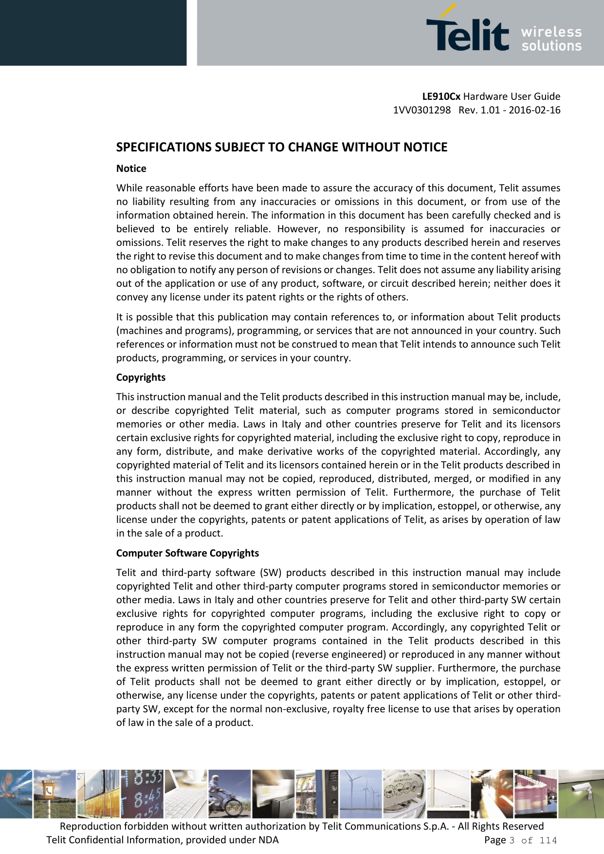


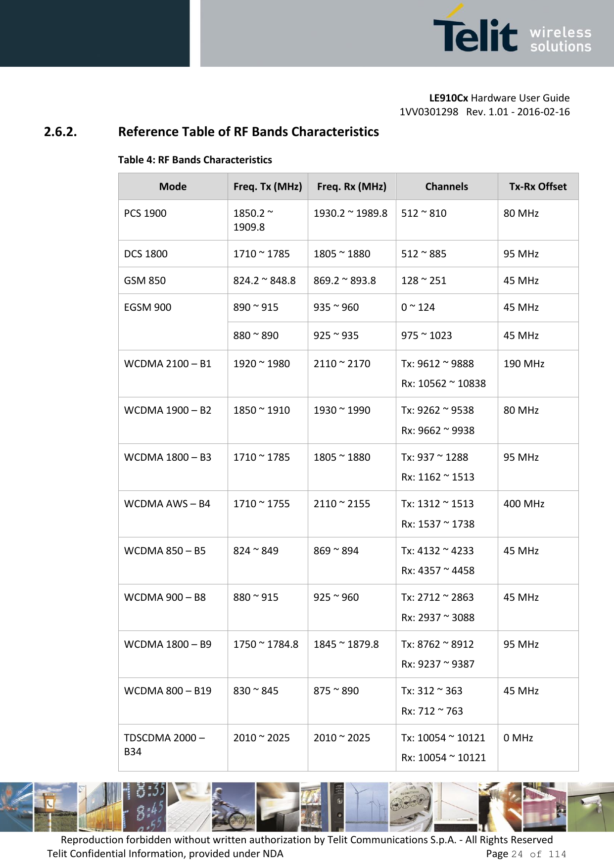


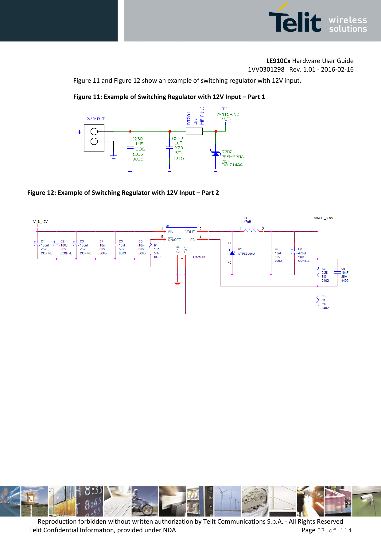
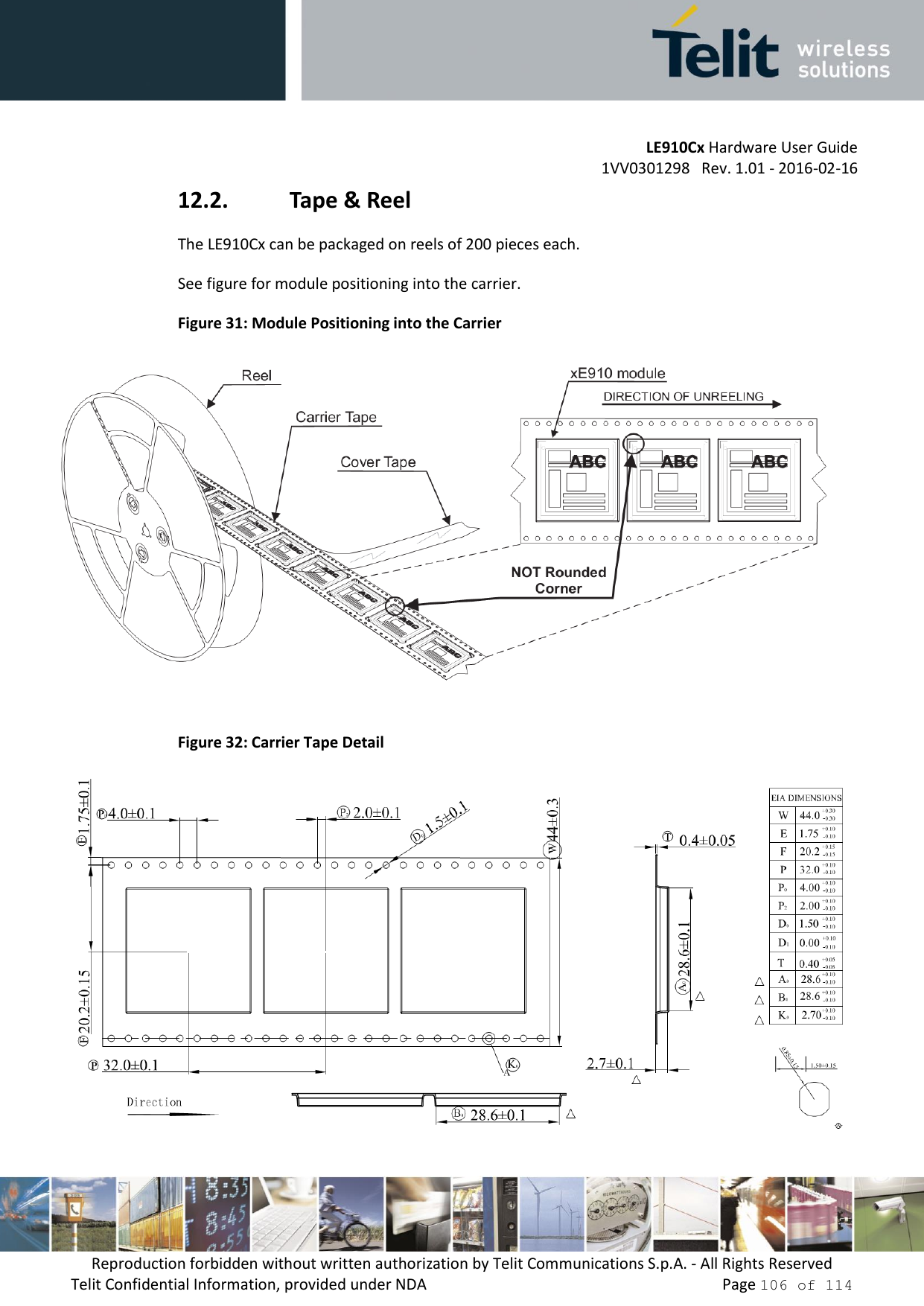
![LE910Cx Hardware User Guide 1VV0301298 Rev. 1.01 - 2016-02-16 Reproduction forbidden without written authorization by Telit Communications S.p.A. - All Rights Reserved Telit Confidential Information, provided under NDA Page 43 of 114 4. Electrical Specifications 4.1. Absolute Maximum Ratings – Not Operational A deviation from the value ranges listed below may harm the LE910Cx module. Table 7: Absolute Maximum Ratings – Not Operational Symbol Parameter Min Max Unit VBATT Battery supply voltage on pin VBATT -0.5 +6.0 [V] VBATT TRANSIENT Transient voltage on pin VBATT (< 10 ms) -0.5 +7.0 [V] VBATT_PA Battery supply voltage on pin VBATT_PA -0.3 +6.0 [V] 4.2. Recommended Operating Conditions Table 8: Recommended Operating Conditions Symbol Parameter Min Typ Max Unit Tamb Ambient temperature -40 +25 +85 [°C] VBATT Battery supply voltage on pin VBATT 3.4 3.8 4.2 [V] VBATT_PA Battery supply voltage on pin VBATT_PA 3.4 3.8 4.2 [V] IBATT_PA + IBATT Peak current to be used to dimension decoupling capacitors on pin VBATT_PA - 80 2000 [mA]](https://usermanual.wiki/Telit-Communications-S-p-A/LE910C1NA/User-Guide-3334829-Page-43.png)
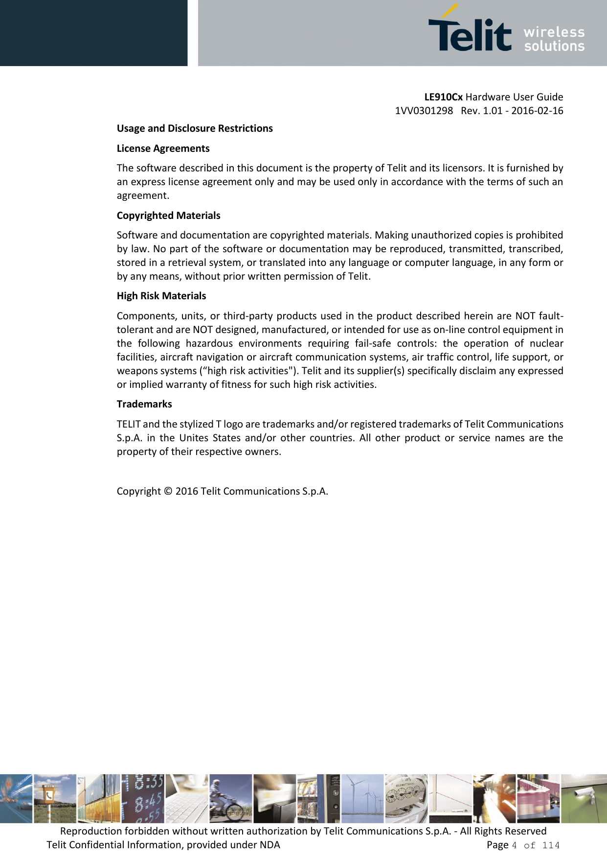
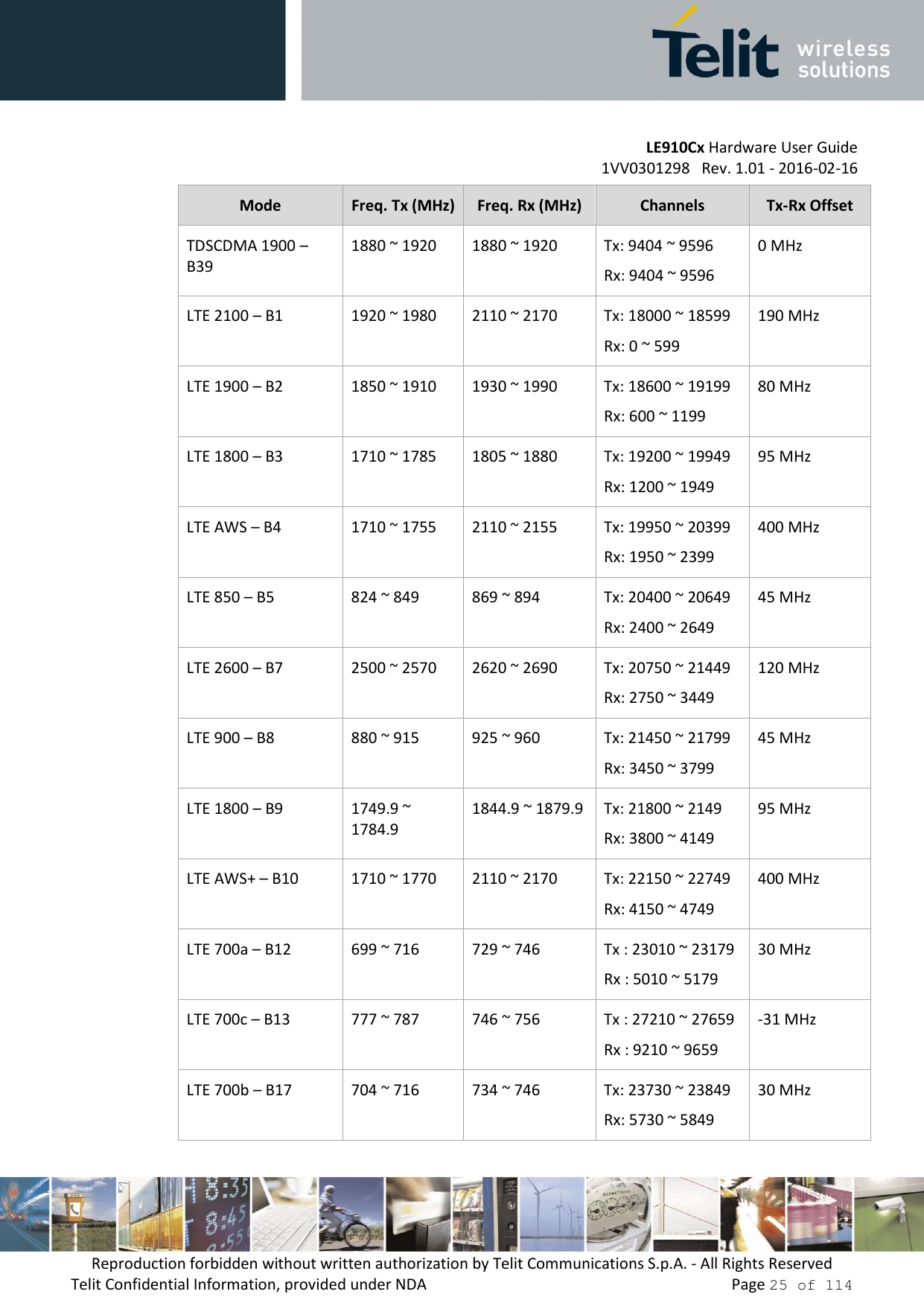
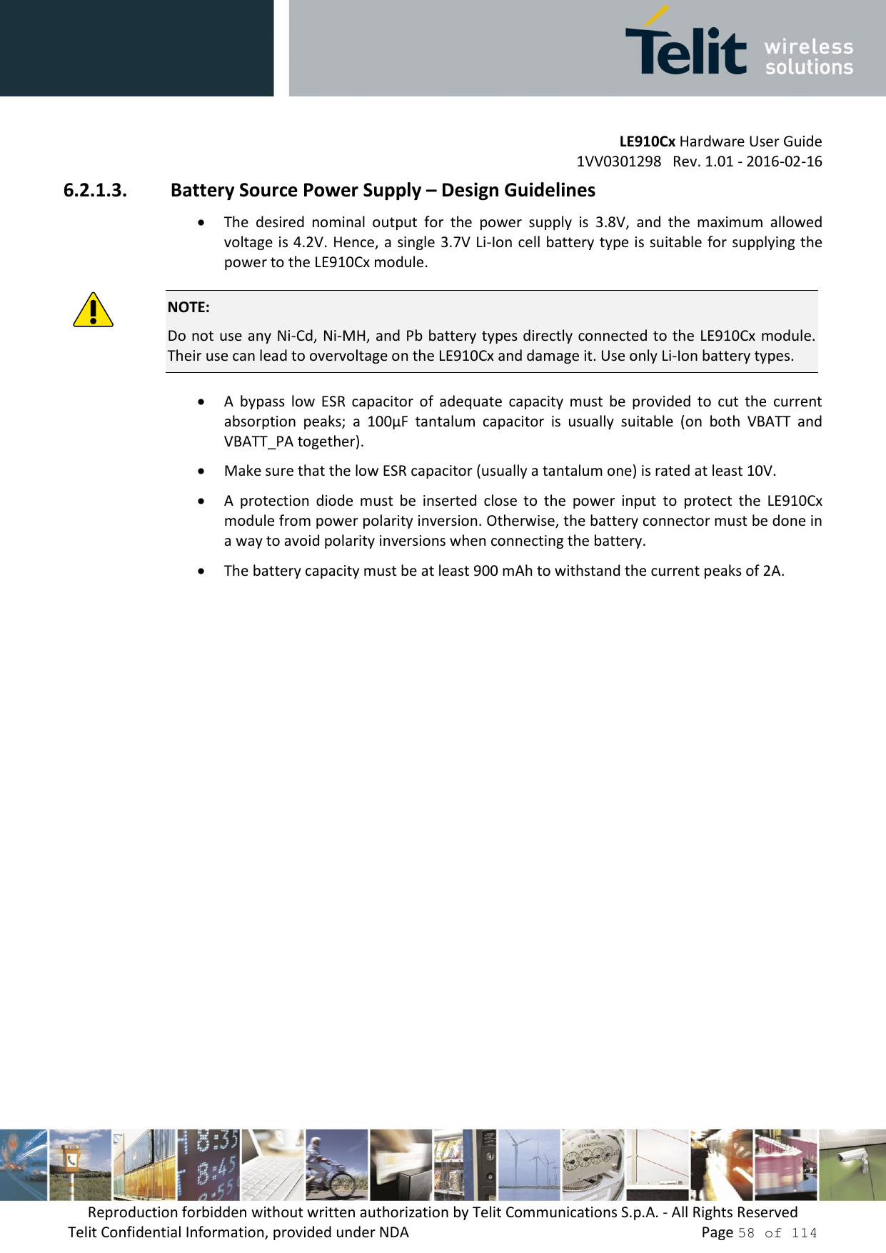
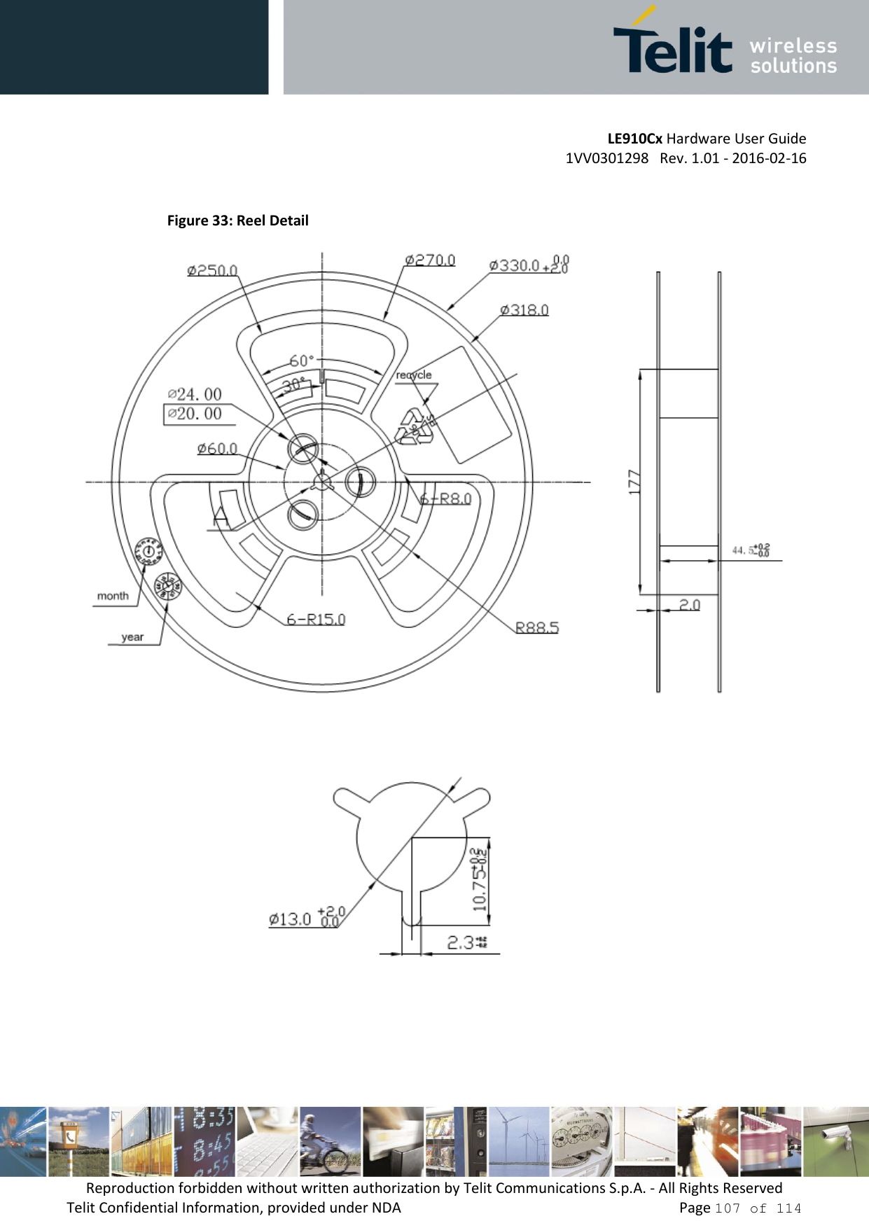
![LE910Cx Hardware User Guide 1VV0301298 Rev. 1.01 - 2016-02-16 Reproduction forbidden without written authorization by Telit Communications S.p.A. - All Rights Reserved Telit Confidential Information, provided under NDA Page 44 of 114 4.3. Logic Level Specifications Unless otherwise specified, all the interface circuits of the LE910Cx are 1.8V CMOS logic. Only few specific interfaces (such as USIM and SD Card) are capable of dual voltage I/O. The following tables show the logic level specifications used in the LE910Cx interface circuits. The data specified in the tables below is valid throughout all drive strengths and the entire temperature ranges. NOTE: Do not connect LE910Cx’s digital logic signal directly to OEM’s digital logic signal with a level higher than 2.7V for 1.8V CMOS signals. 4.3.1. 1.8V Pads - Absolute Maximum Ratings Table 9: Absolute Maximum Ratings - Not Functional Parameter Min Max Input level on any digital pin when on -0.3V +2.16V Input voltage on analog pins when on -0.3V +2.16 V 4.3.2. 1.8V Standard GPIOs Table 10: Operating Range – Interface Levels (1.8V CMOS) Pad Parameter Min Max Unit Comment VIH Input high level 1.25V -- [V] VIL Input low level -- 0.6V [V] VOH Output high level 1.4V -- [V] VOL Output low level -- 0.45V [V] IIL Low-level input leakage current -1 -- [uA] No pull-up IIH High-level input leakage current -- +1 [uA] No pull-down RPU Pull-up resistance 30 390 [kΩ]](https://usermanual.wiki/Telit-Communications-S-p-A/LE910C1NA/User-Guide-3334829-Page-44.png)
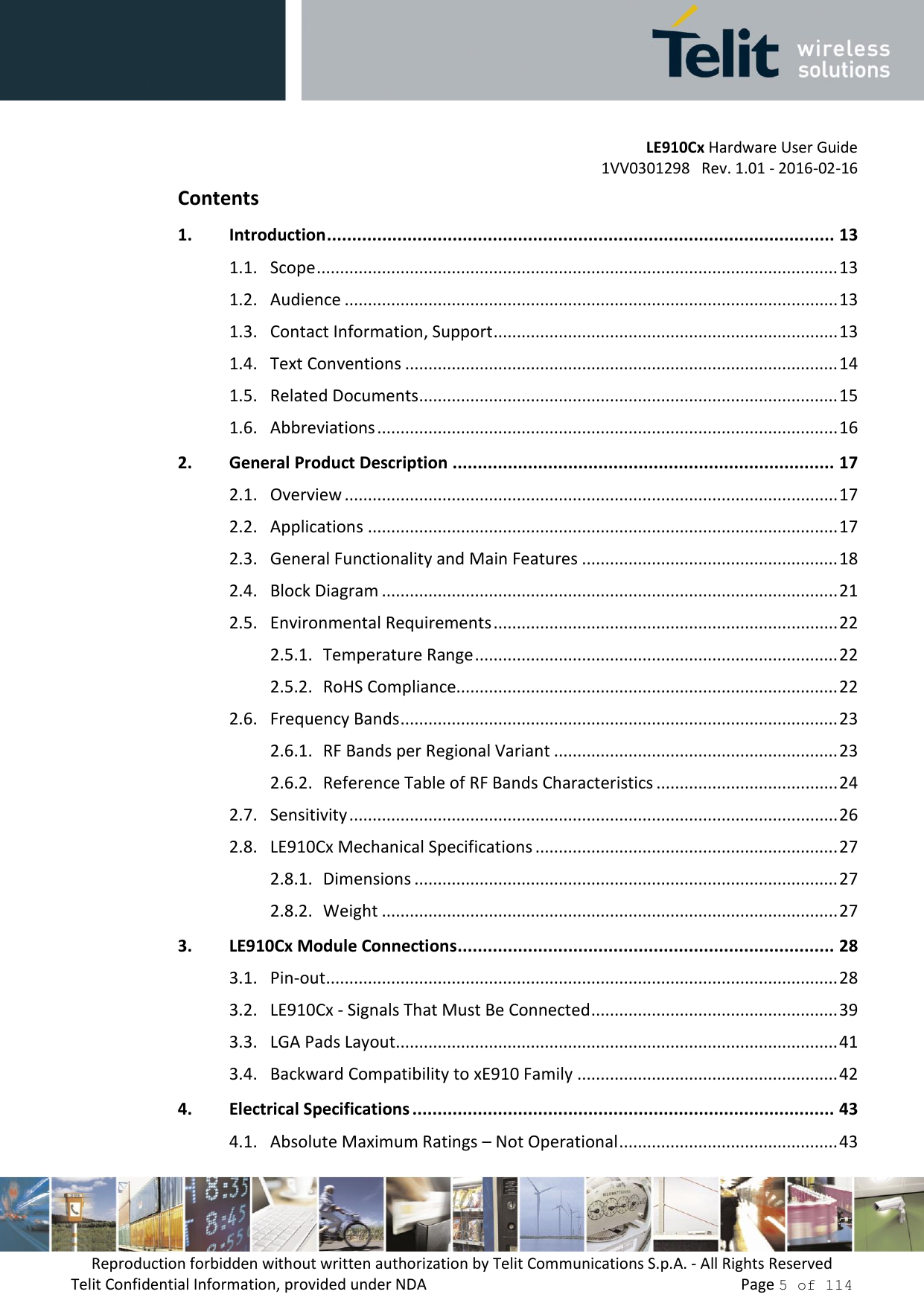
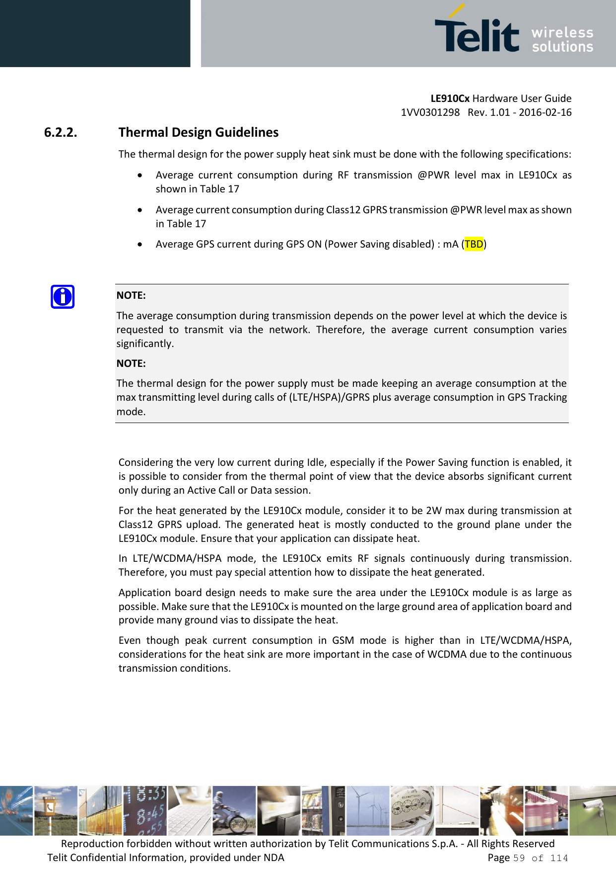
![LE910Cx Hardware User Guide 1VV0301298 Rev. 1.01 - 2016-02-16 Reproduction forbidden without written authorization by Telit Communications S.p.A. - All Rights Reserved Telit Confidential Information, provided under NDA Page 45 of 114 Pad Parameter Min Max Unit Comment RPD Pull-down resistance 30 390 [kΩ] Ci Input capacitance -- 5 [pF] NOTE: Pull-Up and Pull-Down resistance of GPIO3, GPIO7 and GPIO8 is different than above mentioned GPIO3 pull resistance is specified as 10KΩ to 50KΩ 4.3.3. 1.8V SD Card Pads Table 11: Operating Range – SD Card Pads Working at 1.8V Pad Parameter Min Max Unit Comment VIH Input high level 1.27V 2V [V] VIL Input low level -0.3V 0.58V [V] VOH Output high level 1.4V -- [V] VOL Output low level 0 0.45V [V] IIL Low-level input leakage current -2 - [uA] No pull-up IIH High-level input leakage current - 2 [uA] No pull-down RPU Pull-up resistance 10 100 [kΩ] RPD Pull-down resistance 10 100 [kΩ] Ci Input capacitance 5 [pF] 4.3.4. 1.8V SIM Card Pads Table 12: Operating Range – SIM Pads Working at 1.8V Pad Parameter Min Max Unit Comment VIH Input high level 1.35V 2V [V] VIL Input low level -0.3V 0.43V [V] VOH Output high level 1.35V 1.875V [V]](https://usermanual.wiki/Telit-Communications-S-p-A/LE910C1NA/User-Guide-3334829-Page-45.png)
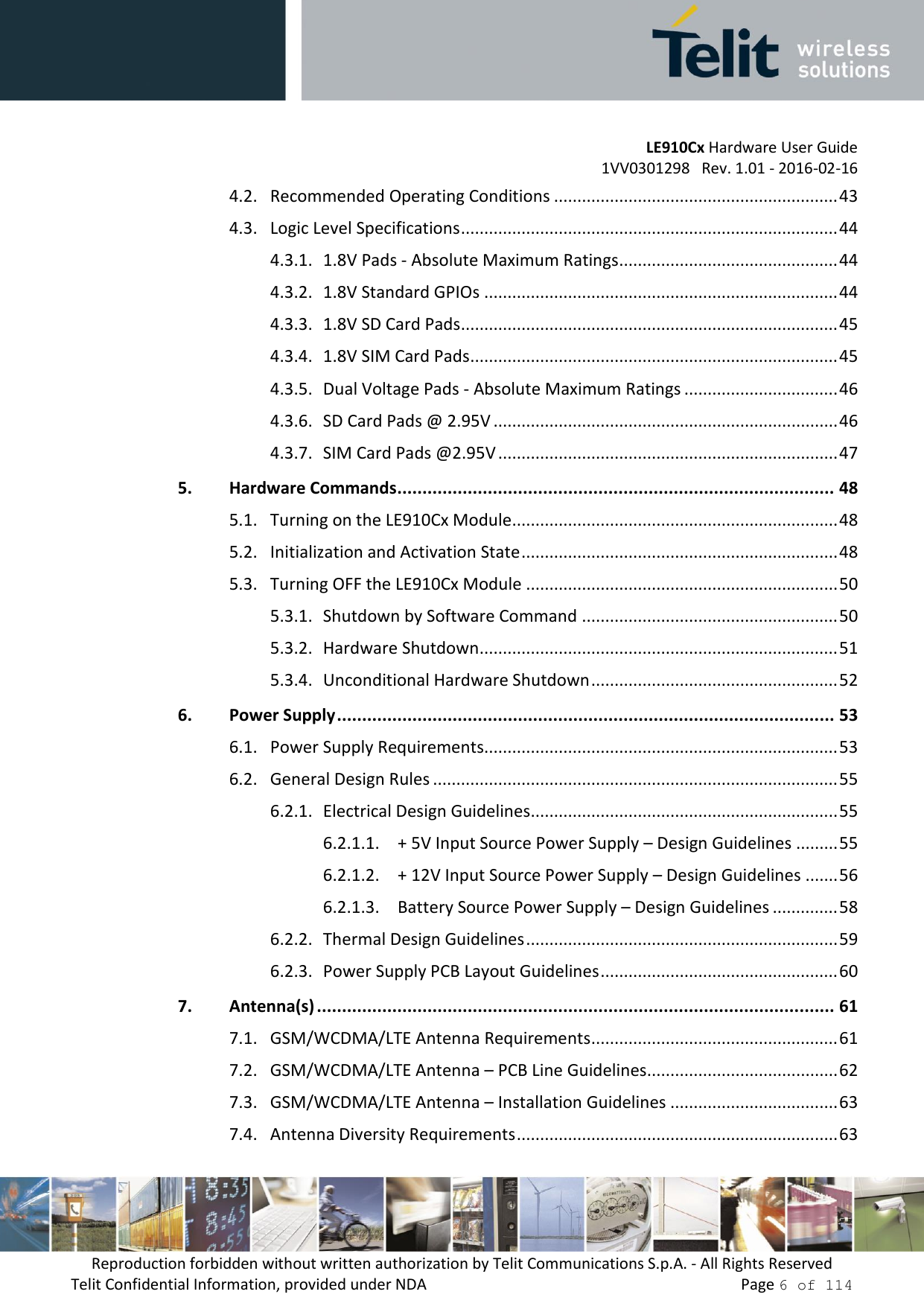
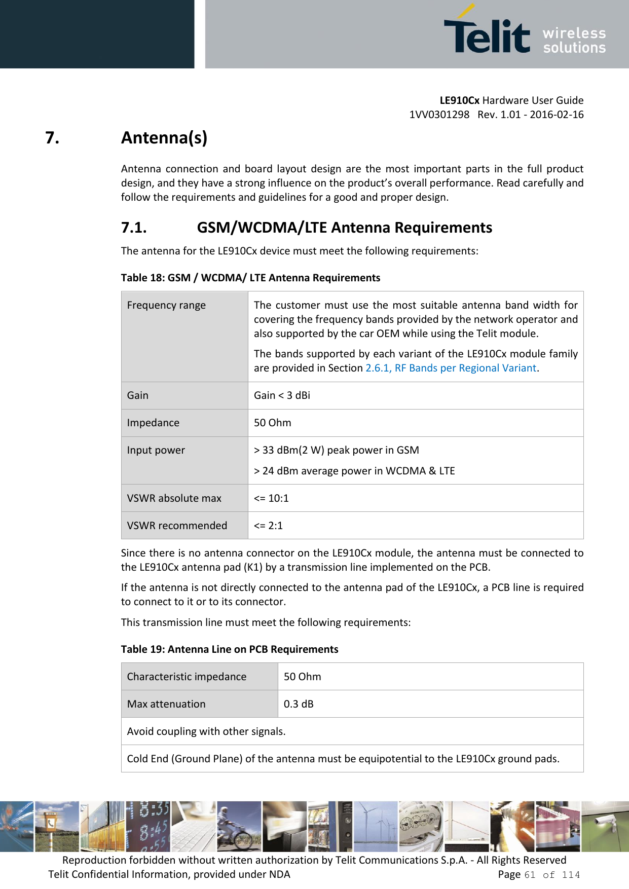
![LE910Cx Hardware User Guide 1VV0301298 Rev. 1.01 - 2016-02-16 Reproduction forbidden without written authorization by Telit Communications S.p.A. - All Rights Reserved Telit Confidential Information, provided under NDA Page 46 of 114 Pad Parameter Min Max Unit Comment VOL Output low level 0V 0.4V [V] IIL Low-level input leakage current -2 - [uA] No pull-up IIH High-level input leakage current - 2 [uA] No pull-down RPU Pull-up resistance 10 100 [kΩ] RPD Pull-down resistance 10 100 [kΩ] Ci Input capacitance 5 [pF] 4.3.5. Dual Voltage Pads - Absolute Maximum Ratings Table 13: Absolute Maximum Ratings - Not Functional Parameter Min Max Input level on any digital pin when on -0.3V +3.6V Input voltage on analog pins when on -0.3V +3.6 V 4.3.6. SD Card Pads @ 2.95V Table 14: Operating Range – For SD Card Pads Operating at 2.95V Pad Parameter Min Max Unit Comments VIH Input high level 1.9V 3.1V [V] VIL Input low level -0.3V 0.7V [V] VOH Output high level 2.1V 3.05V [V] VOL Output low level 0V 0.4V [V] IIL Low-level input leakage current -10 [uA] No pull-up IIH High-level input leakage current 10 [uA] No pull-down RPU Pull-up resistance 10 100 [kΩ]](https://usermanual.wiki/Telit-Communications-S-p-A/LE910C1NA/User-Guide-3334829-Page-46.png)
![LE910Cx Hardware User Guide 1VV0301298 Rev. 1.01 - 2016-02-16 Reproduction forbidden without written authorization by Telit Communications S.p.A. - All Rights Reserved Telit Confidential Information, provided under NDA Page 47 of 114 Pad Parameter Min Max Unit Comments RPD Pull-down resistance 10 100 [kΩ] Ci Input capacitance 5 [pF] 4.3.7. SIM Card Pads @2.95V Table 15: Operating Range – For SIM Pads Operating at 2.95V Pad Parameter Min Max Unit Comment VIH Input high level 2.1V 3.1V [V] VIL Input low level -0.3V 0.55V [V] VOH Output high level 2.25V 3.1V [V] VOL Output low level 0V 0.4V [V] IIL Low-level input leakage current -10 [uA] No pull-up IIH High-level input leakage current 10 [uA] No pull-down RPU Pull-up resistance 10 100 [kΩ] RPD Pull-down resistance 10 100 [kΩ] Ci Input capacitance 5 [pF]](https://usermanual.wiki/Telit-Communications-S-p-A/LE910C1NA/User-Guide-3334829-Page-47.png)
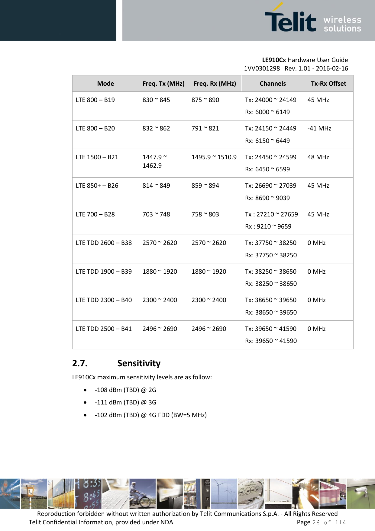
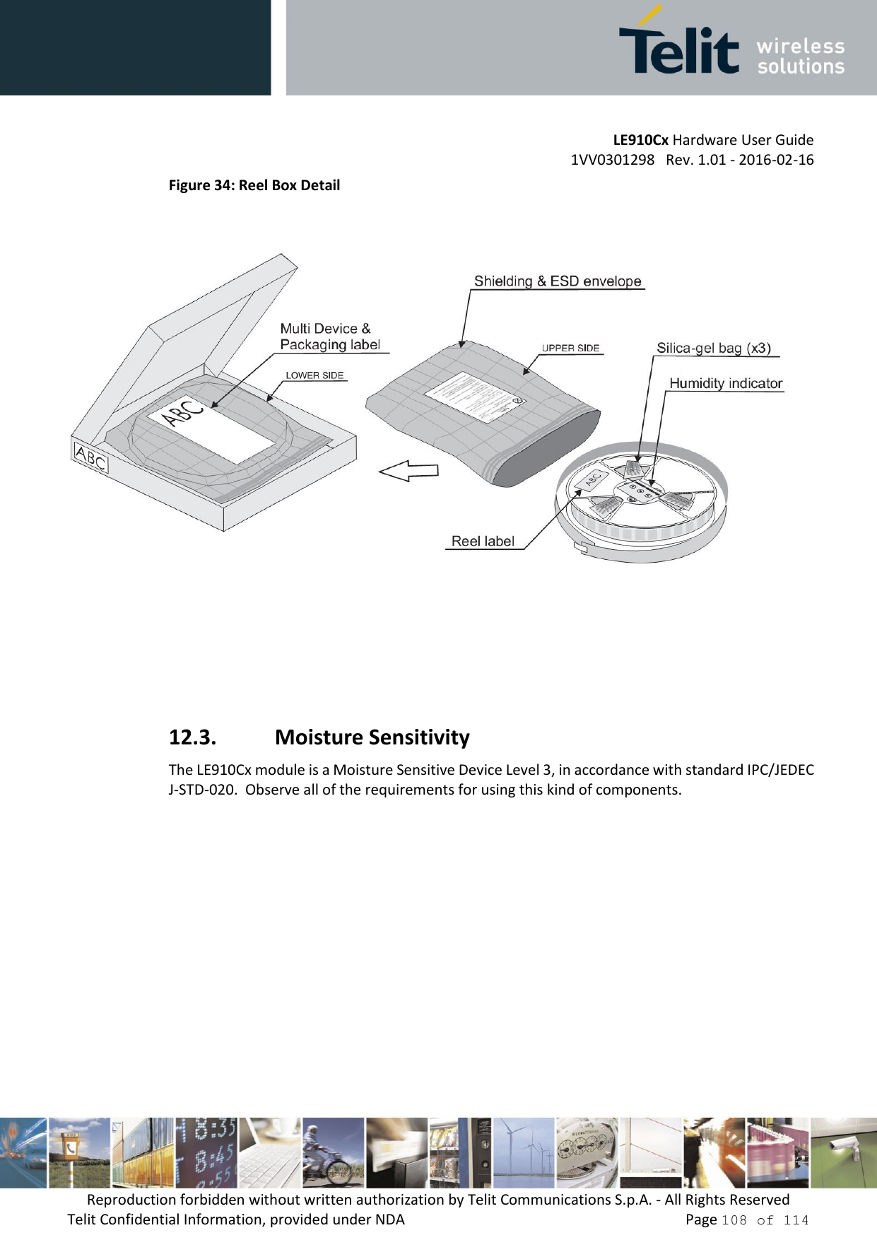
![LE910Cx Hardware User Guide 1VV0301298 Rev. 1.01 - 2016-02-16 Reproduction forbidden without written authorization by Telit Communications S.p.A. - All Rights Reserved Telit Confidential Information, provided under NDA Page 53 of 114 6. Power Supply The power supply circuitry and board layout are very important parts of the full product design, with critical impact on the overall product performance. Read the following requirements and guidelines carefully to ensure a good and proper design. 6.1. Power Supply Requirements The LE910Cx power requirements are as follows: Table 16: Power Supply Requirements Nominal supply voltage 3.8V Supply voltage range 3.4V – 4.2V Max ripple on module input supply 30mV Table 17 provides typical current consumption values of LE910Cx for various operation modes. Table 17: LE910Cx Current Consumption Mode Average [Typical] Mode Description 1) Switched Off Switched off 25µA Module is powered but switched Off (RTC On) 2) IDLE Mode (Standby Mode; No Call in Progress) AT+CFUN=4 1.0mA Tx and Rx are disabled ; module is not registered on the network (Flight mode) DRX GSM 2.0mA DRx2 1.4mA DRx5 WCDMA 1.4mA DRx7 1.2mA DRx8 LTE 1.8mA Paging cycle #128 frames (1.28 sec DRx cycle) 1.4mA Paging cycle #256 frames (2.56 sec DRx cycle)](https://usermanual.wiki/Telit-Communications-S-p-A/LE910C1NA/User-Guide-3334829-Page-53.png)
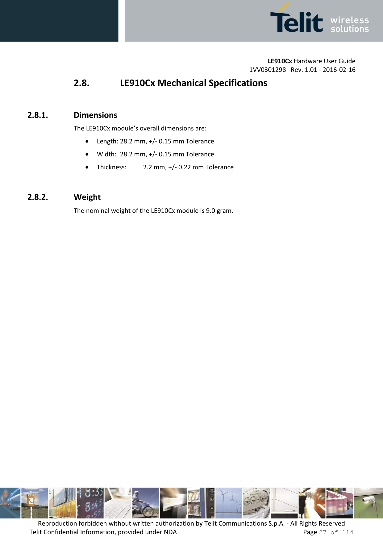
![LE910Cx Hardware User Guide 1VV0301298 Rev. 1.01 - 2016-02-16 Reproduction forbidden without written authorization by Telit Communications S.p.A. - All Rights Reserved Telit Confidential Information, provided under NDA Page 54 of 114 Mode Average [Typical] Mode Description 3) Operative Mode (LTE) LTE (0 dBm) 190mA LTE CAT 4 channel BW 20 MHz, RB=1, Tx = 0 dBm (Test case: BAND 1, Channel 300) LTE (22 dBm) 500mA LTE CAT 4 channel BW 20 MHz, RB=1, Tx = 22 dBm (Test case: BAND 1, Channel 300) 4) Operative Mode (WCDMA) WCDMA Voice 200mA WCDMA voice call (Tx = 10 dBm) WCDMA HSDPA (0 dBm) 150mA WCDMA data call (Cat 14, Tx = 0 dBm, Max throughput) WCDMA HSDPA (22 dBm) 310mA WCDMA data call (Cat 14, Tx = 22 dBm, Max throughput) 5) Operative Mode (GSM) GSM Tx and Rx mode GSM900 PL5 250mA GSM voice call DCS1800 PL0 170mA GPRS 4 Tx + 1 Rx GSM900 PL5 430mA GPRS Sending Data mode (CS-4) DCS1800 PL0 340mA * Worst/best case current values depend on network configuration - not under module control. NOTE: The electrical design for the power supply must ensure a peak current output of at least 2A. NOTE: In GSM/GPRS mode, RF transmission is not continuous, but is packed into bursts at a base frequency of about 216 Hz with relative current peaks as high as about 2A. Therefore, the power supply must be designed to withstand these current peaks without big voltage drops. This means that both the electrical design and the board layout must be designed for this current flow. If the layout of the PCB is not well designed, a strong noise floor is generated on the ground. This will reflect on all the audio paths producing an audible annoying noise at 216 Hz. If the voltage drops during the peaks, current absorption is too high. The device may even shut down as a consequence of the supply voltage drop.](https://usermanual.wiki/Telit-Communications-S-p-A/LE910C1NA/User-Guide-3334829-Page-54.png)


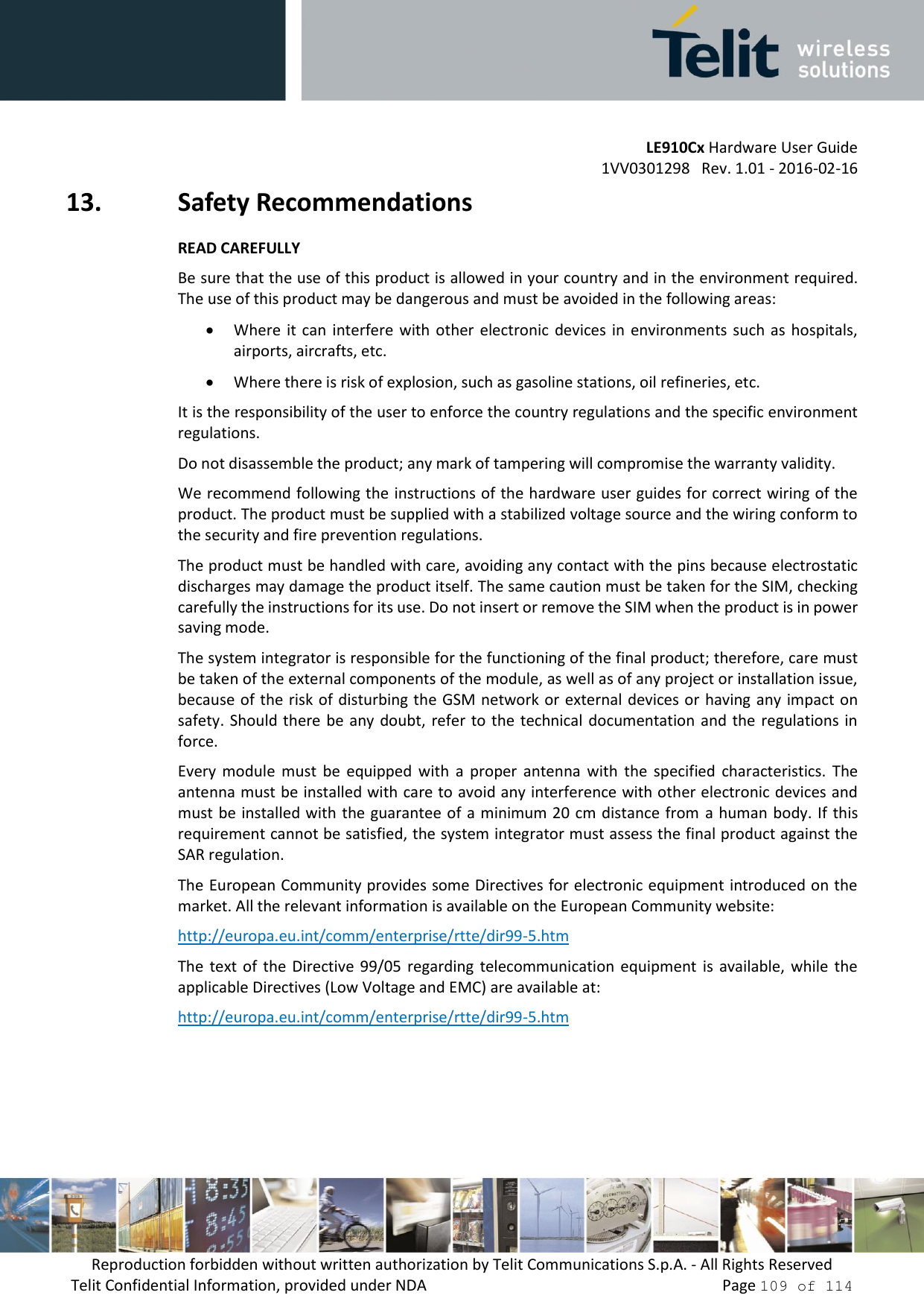
![LE910Cx Hardware User Guide 1VV0301298 Rev. 1.01 - 2016-02-16 Reproduction forbidden without written authorization by Telit Communications S.p.A. - All Rights Reserved Telit Confidential Information, provided under NDA Page 110 of 114 14. Conformity assessment issues14.1. FCC/ISED Regulatory noticesModification statement Telit has not approved any changes or modifications to this device by the user. Any changes or modifications could void the user’s authority to operate the equipment. Telit n’approuve aucune modification apportée à l’appareil par l’utilisateur, quelle qu’en soit la nature. Tout changement ou modification peuvent annuler le droit d’utilisation de l’appareil par l’utilisateur. Interference statement (if it is not placed in the device) This device complies with Part 15 of the FCC Rules and Industry Canada licence-exempt RSS standard(s). Operation is subject to the following two conditions: (1) this device may not cause interference, and (2) this device must accept any interference, including interference that may cause undesired operation of the device. Le présent appareil est conforme aux CNR d'Industrie Canada applicables aux appareils radio exempts de licence. L'exploitation est autorisée aux deux conditions suivantes : (1) l'appareil ne doit pas produire de brouillage, et (2) l'utilisateur de l'appareil doit accepter tout brouillage radioélectrique subi, même si le brouillage est susceptible d'en compromettre le fonctionnement. Wireless notice This device complies with FCC/ISED radiation exposure limits set forth for an uncontrolled environment and meets the FCC radio frequency (RF) Exposure Guidelines and RSS‐102 of the ISED radio frequency (RF) Exposure rules. Antenna gain must be below: Frequency Band Freq [MHz] Gain [dBi] 850 MHz 850 0.63 1900 MHz 1900 2.511700 MHz 1700 5.00700 MHz700 5.63This transmitter must not be co-located or operating in conjunction with any other antenna or transmitter. Le présent appareil est conforme à l'exposition aux radiations FCC / ISED définies pour un environnement non contrôlé et répond aux directives d'exposition de la fréquence de la FCC radiofréquence (RF) et RSS‐102 de la fréquence radio (RF) ISED règles d'exposition. Gain de l'antenne doit être ci-dessous:](https://usermanual.wiki/Telit-Communications-S-p-A/LE910C1NA/User-Guide-3334829-Page-110.png)
![LE910Cx Hardware User Guide 1VV0301298 Rev. 1.01 - 2016-02-16 Reproduction forbidden without written authorization by Telit Communications S.p.A. - All Rights Reserved Telit Confidential Information, provided under NDA Page 111 of 114 L'émetteur ne doit pas être colocalisé ni fonctionner conjointement avec à autre antenne ou autre émetteur. FCC Class B digital device notice This equipment has been tested and found to comply with the limits for a Class B digital device, pursuant to part 15 of the FCC Rules. These limits are designed to provide reasonable protection against harmful interference in a residential installation. This equipment generates, uses and can radiate radio frequency energy and, if not installed and used in accordance with the instructions, may cause harmful interference to radio communications. However, there is no guarantee that interference will not occur in a particular installation. If this equipment does cause harmful interference to radio or television reception, which can be determined by turning the equipment off and on, the user is encouraged to try to correct the interference by one or more of the following measures: -Reorient or relocate the receiving antenna.-Increase the separation between the equipment and receiver.-Connect the equipment into an outlet on a circuit different from that to which the receiveris connected.-Consult the dealer or an experienced radio/TV technician for help.Labelling Requirements for the Host device The host device shall be properly labelled to identify the modules within the host device. The certification label of the module shall be clearly visible at all times when installed in the host device, otherwise the host device must be labelled to display the FCC ID and IC of the module, preceded by the words "Contains transmitter module", or the word "Contains", or similar wording expressing the same meaning, as follows: Contains FCC ID: RI7LE910C1NA Contains IC: 5131A-LE910C1NAL'appareil hôte doit être étiqueté comme il faut pour permettre l'identification des modules qui s'y trouvent. L'étiquette de certification du module donné doit être posée sur l'appareil hôte à un endroit bien en vue en tout temps. En l'absence d'étiquette, l'appareil hôte doit porter une étiquette donnant le FCC ID et le IC du module, précédé des mots « Contient un module d'émission », du mot « Contient » ou d'une formulation similaire exprimant le même sens, comme suit :Contains FCC ID: RI7LE910C1NA Contains IC: 5131A-LE910C1NA Frequency Band Freq [MHz] Gain [dBi] 850 MHz 850 0.63 1900 MHz 1900 2.511700 MHz 1700 5.00700 MHz700 5.63](https://usermanual.wiki/Telit-Communications-S-p-A/LE910C1NA/User-Guide-3334829-Page-111.png)