Telit Communications S p A LE920A4NA Wireless Module User Manual 1vv0301261 LE920A4 HW User Guide r4 3
Telit Communications S.p.A. Wireless Module 1vv0301261 LE920A4 HW User Guide r4 3
Contents
- 1. User Manual
- 2. User manual
User manual

LE920A4 Auto
HW User Guide
Doc#: 1VV0301261
Rev. 4.3 – 2017-12-07

LE920A4 HW User Guide
Doc#: 1VV0301261
Rev. 4.3 Page 2 of 123 2017-12-07
SPECIFICATIONS ARE SUBJECT TO CHANGE WITHOUT NOTICE
NOTICE
While reasonable efforts have been made to assure the accuracy of this document, Telit
assumes no liability resulting from any inaccuracies or omissions in this document, or from
use of the information obtained herein. The information in this document has been carefully
checked and is believed to be reliable. However, no responsibility is assumed for
inaccuracies or omissions. Telit reserves the right to make changes to any products
described herein and reserves the right to revise this document and to make changes from
time to time in content hereof with no obligation to notify any person of revisions or changes.
Telit does not assume any liability arising out of the application or use of any product,
software, or circuit described herein; neither does it convey license under its patent rights
or the rights of others.
It is possible that this publication may contain references to, or information about Telit
products (machines and programs), programming, or services that are not announced in
your country. Such references or information must not be construed to mean that Telit
intends to announce such Telit products, programming, or services in your country.
COPYRIGHTS
This instruction manual and the Telit products described in this instruction manual may be,
include or describe copyrighted Telit material, such as computer programs stored in
semiconductor memories or other media. Laws in the Italy and other countries preserve for
Telit and its licensors certain exclusive rights for copyrighted material, including the
exclusive right to copy, reproduce in any form, distribute and make derivative works of the
copyrighted material. Accordingly, any copyrighted material of Telit and its licensors
contained herein or in the Telit products described in this instruction manual may not be
copied, reproduced, distributed, merged or modified in any manner without the express
written permission of Telit. Furthermore, the purchase of Telit products shall not be deemed
to grant either directly or by implication, estoppel, or otherwise, any license under the
copyrights, patents or patent applications of Telit, as arises by operation of law in the sale
of a product.
COMPUTER SOFTWARE COPYRIGHTS
The Telit and 3rd Party supplied Software (SW) products described in this instruction
manual may include copyrighted Telit and other 3rd Party supplied computer programs
stored in semiconductor memories or other media. Laws in the Italy and other countries
preserve for Telit and other 3rd Party supplied SW certain exclusive rights for copyrighted
computer programs, including the exclusive right to copy or reproduce in any form the
copyrighted computer program. Accordingly, any copyrighted Telit or other 3rd Party
supplied SW computer programs contained in the Telit products described in this instruction
manual may not be copied (reverse engineered) or reproduced in any manner without the
express written permission of Telit or the 3rd Party SW supplier. Furthermore, the purchase
of Telit products shall not be deemed to grant either directly or by implication, estoppel, or
otherwise, any license under the copyrights, patents or patent applications of Telit or other
3rd Party supplied SW, except for the normal non-exclusive, royalty free license to use that
arises by operation of law in the sale of a product.

LE920A4 HW User Guide
Doc#: 1VV0301261
Rev. 4.3 Page 3 of 123 2017-12-07
USAGE AND DISCLOSURE RESTRICTIONS
I. License Agreements
The software described in this document is the property of Telit and its licensors. It is
furnished by express license agreement only and may be used only in accordance with the
terms of such an agreement.
II. Copyrighted Materials
Software and documentation are copyrighted materials. Making unauthorized copies is
prohibited by law. No part of the software or documentation may be reproduced,
transmitted, transcribed, stored in a retrieval system, or translated into any language or
computer language, in any form or by any means, without prior written permission of Telit
III. High Risk Materials
Components, units, or third-party products used in the product described herein are NOT
fault-tolerant and are NOT designed, manufactured, or intended for use as on-line control
equipment in the following hazardous environments requiring fail-safe controls: the
operation of Nuclear Facilities, Aircraft Navigation or Aircraft Communication Systems, Air
Traffic Control, Life Support, or Weapons Systems (High Risk Activities"). Telit and its
supplier(s) specifically disclaim any expressed or implied warranty of fitness for such High
Risk Activities.
IV. Trademarks
TELIT and the Stylized T Logo are registered in Trademark Office. All other product or
service names are the property of their respective owners.
V. Third Party Rights
The software may include Third Party Right software. In this case you agree to comply with
all terms and conditions imposed on you in respect of such separate software. In addition
to Third Party Terms, the disclaimer of warranty and limitation of liability provisions in this
License shall apply to the Third Party Right software.
TELIT HEREBY DISCLAIMS ANY AND ALL WARRANTIES EXPRESS OR IMPLIED
FROM ANY THIRD PARTIES REGARDING ANY SEPARATE FILES, ANY THIRD PARTY
MATERIALS INCLUDED IN THE SOFTWARE, ANY THIRD PARTY MATERIALS FROM
WHICH THE SOFTWARE IS DERIVED (COLLECTIVELY “OTHER CODE”), AND THE
USE OF ANY OR ALL THE OTHER CODE IN CONNECTION WITH THE SOFTWARE,
INCLUDING (WITHOUT LIMITATION) ANY WARRANTIES OF SATISFACTORY
QUALITY OR FITNESS FOR A PARTICULAR PURPOSE.
NO THIRD PARTY LICENSORS OF OTHER CODE SHALL HAVE ANY LIABILITY FOR
ANY DIRECT, INDIRECT, INCIDENTAL, SPECIAL, EXEMPLARY, OR CONSEQUENTIAL
DAMAGES (INCLUDING WITHOUT LIMITATION LOST PROFITS), HOWEVER CAUSED
AND WHETHER MADE UNDER CONTRACT, TORT OR OTHER LEGAL THEORY,
ARISING IN ANY WAY OUT OF THE USE OR DISTRIBUTION OF THE OTHER CODE
OR THE EXERCISE OF ANY RIGHTS GRANTED UNDER EITHER OR BOTH THIS
LICENSE AND THE LEGAL TERMS APPLICABLE TO ANY SEPARATE FILES, EVEN IF
ADVISED OF THE POSSIBILITY OF SUCH DAMAGES.

LE920A4 HW User Guide
Doc#: 1VV0301261
Rev. 4.3 Page 4 of 123 2017-12-07
APPLICABILITY TABLE
This documentation applies to the following products:
Table 1: Applicability Table
Module Name Description
LE920A4-NA North America regional variant (AT&T, T-Mobile)
LE920A4-NV (*)
North America regional variant (Verizon)
LE920A4-EU Europe regional variant
HE920A-EU (*) Non-LTE Europe variant
LE920A4-CN China variant
LE920A4-AP (*) APAC variant
(*) Variants which were not designed yet
LE920A4 HW User Guide
Doc#: 1VV0301261
Rev. 4.3 Page 5 of 123 2017-12-07
CONTENTS
1. INTRODUCTION .............................................................................................9
Scope ............................................................................................................. 9
Audience......................................................................................................... 9
Contact Information, Support .......................................................................... 9
Text Conventions ...........................................................................................10
Related Documents .......................................................................................11
2. GENERAL PRODUCT DESCRIPTION ......................................................... 12
Overview........................................................................................................12
Applications ...................................................................................................12
General Functionality and Main Features.......................................................13
Block Diagram ...............................................................................................15
Environmental Requirements .........................................................................17
2.5.1. Temperature Range .......................................................................................17
2.5.2. RoHS Compliance .........................................................................................17
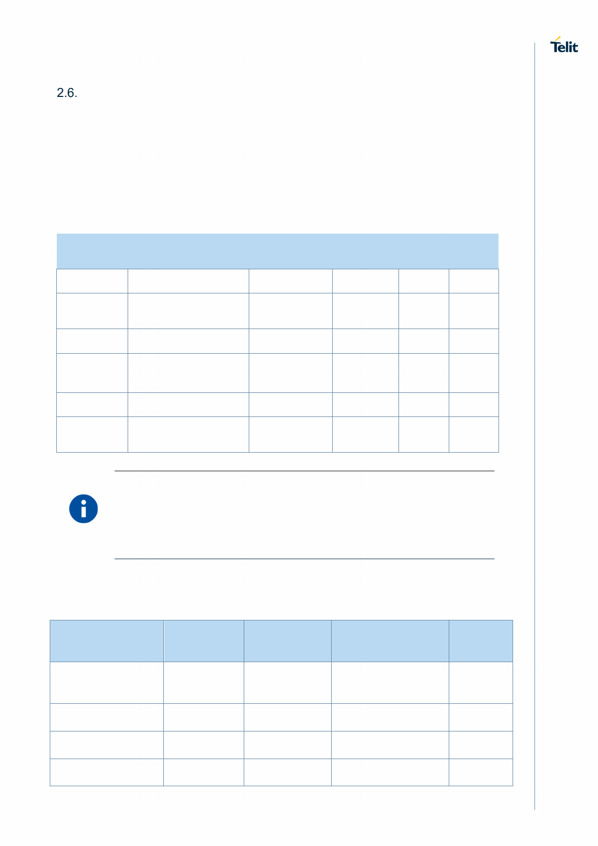
Frequency Bands ...........................................................................................18
2.6.1. RF Bands per Regional Variant .....................................................................18
2.6.2. Reference Table of RF Bands Characteristics ...............................................18
RF parameters ...............................................................................................21
2.7.1. Sensitivity ......................................................................................................21
2.7.2. Output power .................................................................................................21
Mechanical Dimensions .................................................................................22
Weight ...........................................................................................................22
3. MODULE CONNECTIONS ............................................................................ 23
Pin-out ...........................................................................................................23
Signals That Must Be Connected ...................................................................37
LE940A4 LGA Pads Layout ...........................................................................40
4. ELECTRICAL SPECIFICATIONS ................................................................. 41
Absolute Maximum Ratings – Not Operational ...............................................41
Recommended Operating Conditions ............................................................41
Logic Level Specifications ..............................................................................41
4.3.1. 1.8V Pads - Absolute Maximum Ratings ........................................................42
4.3.2. 1.8V Standard GPIOs ....................................................................................42
4.3.3. 1.8V SD Card Pads .......................................................................................43
4.3.4. 1.8V SIM Card Pads ......................................................................................43
4.3.5. Dual Voltage Pads - Absolute Maximum Ratings ...........................................44

LE920A4 HW User Guide
Doc#: 1VV0301261
Rev. 4.3 Page 6 of 123 2017-12-07
4.3.6. SD Card Pads @ 2.95V .................................................................................44
4.3.7. SIM Card Pads @2.95V.................................................................................44
5. HARDWARE COMMANDS ........................................................................... 46
Turning on the Module ...................................................................................46
Initialization and Activation State ...................................................................46
Turning off the Module ...................................................................................48
5.3.1. Shutdown by Software Command ..................................................................49
5.3.2. Hardware Shutdown ......................................................................................49
5.3.3. Unconditional Hardware Reset ......................................................................51
5.3.4. Unconditional Hardware Shutdown ................................................................52
6. POWER SUPPLY .......................................................................................... 54
Power Supply Requirements ..........................................................................54
General Design Rules ....................................................................................56
6.2.1. Electrical Design Guidelines ..........................................................................56
6.2.1.1. + 5V Input Source Power Supply Design Guidelines ......................................56
6.2.1.2. + 12V Input Source Power Supply Design Guidelines ....................................57
6.2.1.3. Battery Source Power Supply Design Guidelines ...........................................59
6.2.2. Thermal Design Guidelines ............................................................................59
6.2.3. Power Supply PCB Layout Guidelines ...........................................................60
7. ANTENNA(S) ................................................................................................ 62
GSM/WCDMA/TD-SCDMA/LTE Antenna Requirements ...............................62
GSM/WCDMA/TD-SCDMA/LTE Antenna – PCB Line Guidelines ..................63
GSM/WCDMA/TD-SCDMA/LTE Antenna – Installation Guidelines ................64
Antenna Diversity Requirements ....................................................................64
GPS/GNSS Antenna Requirements ...............................................................65
7.5.1. Combined GPS/GNSS Antenna .....................................................................65
7.5.2. Linear and Patch GPS/GNSS Antenna ..........................................................66
7.5.3. Front End Design Considerations ..................................................................66
7.5.4. GPS/GNSS Antenna – PCB Line Guidelines .................................................66
7.5.5. GPS/GNSS Antenna – Installation Guidelines ...............................................67
8. HARDWARE INTERFACES .......................................................................... 68
USB Port........................................................................................................69
8.1.1. USB OTG support ..........................................................................................70
HSIC Interface ...............................................................................................70
Ethernet Connectivity (optional) .....................................................................71
8.3.1. SGMII Interface..............................................................................................71
8.3.2. Ethernet Control Interface ..............................................................................71
LE920A4 HW User Guide
Doc#: 1VV0301261
Rev. 4.3 Page 7 of 123 2017-12-07
Serial Ports ....................................................................................................72
8.4.1. Modem Serial Port 1 ......................................................................................72
8.4.2. Modem Serial Port 2 ......................................................................................74
8.4.3. RS232 Level Translation ................................................................................75
Peripheral Ports .............................................................................................77
8.5.1. SPI – Serial Peripheral Interface ....................................................................77
8.5.2. I2C - Inter-integrated Circuit ...........................................................................78
8.5.3. SD/MMC Card Interface .................................................................................78
8.5.4. WiFi (SDIO) Control Interface ........................................................................80
Audio Interface ..............................................................................................81
8.6.1. Analog Audio .................................................................................................81
8.6.2. Analog Audio Characteristics .........................................................................82
8.6.2.1. Analog Inputs Characteristics ........................................................................82
8.6.2.2. Analog Output Characteristics .......................................................................84
8.6.3. Digital Audio ..................................................................................................85
8.6.3.1. Short Frame Timing Diagrams .......................................................................86
8.6.3.2. Long Frame Timing Diagrams ........................................................................88
General Purpose I/O ......................................................................................90
8.7.1. Using a GPIO Pad as Input ............................................................................91
8.7.2. Using a GPIO Pad as an Interrupt Source .....................................................92
8.7.3. Using a GPIO Pad as Output .........................................................................92
9. MISCELLANEOUS FUNCTIONS .................................................................. 93
Indication of Network Service Availability .......................................................93
RTC – Real Time Clock .................................................................................93
VAUX Power Output ......................................................................................93
ADC Converter ..............................................................................................95
9.4.1. Description .....................................................................................................95
9.4.2. Using ADC Converter ....................................................................................95
Using the Temperature Monitor Function .......................................................95
Fuel Gauge (optional) ....................................................................................95
GNSS Characteristics ....................................................................................97
10. MOUNTING THE MODULE ON YOUR BOARD ........................................... 98
General ..........................................................................................................98
Finishing & Dimensions .................................................................................98
Recommended Foot Print for the Application .................................................99
Stencil ............................................................................................................99
PCB Pad Design .......................................................................................... 100
Recommendations for PCB Pad Dimensions (mm) ...................................... 100
LE920A4 HW User Guide
Doc#: 1VV0301261
Rev. 4.3 Page 8 of 123 2017-12-07
Solder Paste ................................................................................................ 101
10.7.1. Solder Reflow .............................................................................................. 101
11. APPLICATION GUIDE ................................................................................ 103
Debug of the Module in Production .............................................................. 103
Bypass Capacitor on Power Supplies .......................................................... 104
SIM Interface ............................................................................................... 105
11.3.1. SIM Schematic Example .............................................................................. 105
EMC Recommendations .............................................................................. 105
Download and Debug Port ........................................................................... 106
11.5.1. Fast Boot Mode ........................................................................................... 106
11.5.2. Recovery Boot Mode ................................................................................... 106
Antenna Detection ....................................................................................... 107
12. PACKING SYSTEM .................................................................................... 108
Tray ............................................................................................................. 108
Tape & Reel ................................................................................................. 111
Moisture Sensitivity ...................................................................................... 112
13. SAFETY RECOMMENDATIONS................................................................. 113
14. CONFORMITY ASSESSMENT ISSUES ..................................................... 114
FCC/ISED Regulatory notices ...................................................................... 114
15. ACRONYMS ................................................................................................ 116
16. DOCUMENT HISTORY ............................................................................... 119

LE920A4 HW User Guide Introduction
Doc#: 1VV0301261 Scope
Rev. 4.3 Page 9 of 123 2017-12-07
1. Introduction
Scope
This document introduces the Telit LE920A4 module and presents possible and
recommended hardware solutions for developing a product based on this module. All the
features and solutions detailed in this document are applicable to all module variants,
where “module” refers to the variants listed in the applicability table.
If a specific feature is applicable to a specific product only, it will be clearly marked.
NOTE:
Module refers to all modules listed in the Applicability Table.
This document takes into account all the basic functions of a wireless module; a valid
hardware solution is suggested for each function, and incorrect solutions and common
errors to be avoided are pointed out.
Obviously, this document cannot embrace every hardware solution or every product that
can be designed. Obviously, avoiding invalid solutions must be considered mandatory.
Where the suggested hardware configurations need not be considered mandatory, the
information given should be used as a guide and a starting point for properly developing
your product with the Telit module.
NOTE:
The integration of the module within a user application must be done
according to the design rules described in this manual.
Audience
This document is intended for Telit customers, especially system integrators, about to
implement their applications using the Telit module.
Contact Information, Support
For general contact, technical support services, technical questions and report
documentation errors, contact Telit Technical Support at:
• TS-EMEA@telit.com
• TS-AMERICAS@telit.com
• TS-APAC@telit.com
• TS-SRD@telit.com

LE920A4 HW User Guide Introduction
Doc#: 1VV0301261 Text Conventions
Rev. 4.3 Page 10 of 123 2017-12-07
Alternatively, use:
http://www.telit.com/support
For detailed information about where you can buy the Telit modules or for
recommendations on accessories and components visit:
http://www.telit.com
To register for product news and announcements or for product questions contact Telit’s
Technical Support Center (TTSC).
Our aim is to make this guide as helpful as possible. Keep us informed of your comments
and suggestions for improvements.
Telit appreciates feedback from the users of our information.
Text Conventions
The following conventions are used to emphasize specific types of information:
DANGER:
Danger – This information MUST be followed or catastrophic equipment
failure or bodily injury may occur.
WARNING:
Caution or Warning – Alerts the user to important points about integrating the
module, if these points are not followed, the module and end user equipment
may fail or malfunction.
NOTE:
Tip or Information – Provides advice and suggestions that may be useful
when integrating the module.
All dates are in ISO 8601 format, i.e. YYYY-MM-DD.

LE920A4 HW User Guide Introduction
Doc#: 1VV0301261 Related Documents
Rev. 4.3 Page 11 of 123 2017-12-07
Related Documents
Table 2: Related Documents
Document Title Document Number
Ref 1: LE920A4 AT Command User Guide 80490ST10778A
Ref 2: LE920A4 Software Guide 1VV0301332
Ref 3: Generic EVB HW User Guide 1VV0301249
Ref 4: LE920A4 Interface Board HW User Guide 1VV0301248
Ref 5: Digital Voice Interface_Application_Note 80000NT11246A
Ref 6: Telit_LE920A4_LE910Cx_Wi-
Fi_Interface_Application_Note_r1
80490NT11511A
Ref 7: Antenna Detection Application Note 80000NT10002A
Ref 8: High-Speed Inter-Chip USB Electrical Specification,
version 1.0
(a supplement to the USB 2.0 specification, Section 3.8.2)
Ref 9: ETH_Expansion_board_Application Note 80490NT11622A

LE920A4 HW User Guide General Product Description
Doc#: 1VV0301261 Overview
Rev. 4.3 Page 12 of 123 2017-12-07
2. General Product Description
Overview
The LE920A4 module is Telit’s platform for automotive telematics on-board units (OBU's)
for applications, such as automotive telematics and eCall, based on the following
technologies:
• 4G cellular for voice and data communication
• GNSS (optional) - GPS, GLONASS, BeiDou, Galileo, QZSS, for positioning
service
• Embedded security
o ARM Trust Zone services (optional)
• Designed for automotive markets
1
quality needs
In its most basic use case, the module can be applied as a wireless communication front-
end for telematics products, offering GNSS and mobile communication features to an
external host CPU through its rich interfaces.
The module can further support customer software applications and security features. The
module provides a software application development environment with sufficient system
resources for creating rich on-board applications. Thanks to a dedicated application
processor and embedded security resources, product developers and manufacturers can
create products that guarantee fraud prevention and tamper evidence without extra effort
for additional security precautions.
The module can be self-sufficient and serve as a fully integrated solution for applications,
such as location-based cellular telematics, navigation, road pricing and eCall. In such a
case, the customer would simply complement the module with a power supply, speaker
amplifier, microphone, antennas, and an HMI (if applicable).
The module is available in hardware variants as listed in Table 1: Applicability Table. The
designated RF band sets per each variant are detailed in Section 2.6, Frequency Bands.
Applications
The module can be used for telematics applications where tamper-resistance,
confidentiality, integrity, and authenticity of end-user information are required, for
example:
• Emergency call
• Telematics services
• Road pricing
• Pay-as-you-drive insurance
• Stolen vehicles tracking
• Internet connectivity
1
In accordance with Telit’s Robustness Validation, using AEC-Q100-defined qualification tests

LE920A4 HW User Guide General Product Description
Doc#: 1VV0301261 General Functionality and Main Features
Rev. 4.3 Page 13 of 123 2017-12-07
General Functionality and Main Features
The LE920A4 family of automotive cellular modules features an advanced LTE and multi-
RAT modem together with a powerful on-chip application processor and a rich set of
interfaces.
The major functions and features are listed below:
Table 3: Main Features
Function Features
Modem • Multi-RAT cellular modem for voice and data communication
o LTE FDD/TDD Cat4 (150/50 Mbps DL/UL)
o GSM/GPRS/EDGE
o WCDMA up to DC HSPA+, Rel.9
o TD-SCDMA (China variant only)
• Support for European eCall , US E911, and ERA Glonass
• Support for SIM profile switching
• Regional variants with optimal choice of RF bands for
worldwide coverage of countries and MNOs
• State-of-the-art GNSS solution with
GPS/GLONASS/BeiDou/Galileo/QZSS receiver
Audio
subsystem
• Embedded analog codec with two microphone inputs
• Embedded analog codec with one stereo or two mono
outputs
• PCM/I2S digital audio interface
•
Up to 48
kHz sample rate, 16 bit words
Two USIM ports
– dual voltage
• Class B and Class C support
• Hot-swap support
•
Data rates up to 4 MHz
Application
processor Application processor to run customer application code
• 32 bit ARM Cortex-A7 up to 1.2 GHz running the Linux
operating system
• Flash + DDR are large enough to allow for customer’s own
software applications
• Default memory configuration is 4 Gb (512 MB) Flash + 2 Gb
(256 MB) RAM
• Other memory configurations can be supported upon request,
for example: 2 Gbit Flash + 2 Gbit DDR or 4 Gbit Flash +
4
Gbit DDR.

LE920A4 HW User Guide General Product Description
Doc#: 1VV0301261 General Functionality and Main Features
Rev. 4.3 Page 14 of 123 2017-12-07
Function Features
Interfaces Rich set of interfaces, including:
• SD/MMC Card Interface supporting SD3.0 standard
• SDIO for external WiFi transceiver supporting SDIO3.0
standard
• SGMII for external Ethernet transceiver (optional)
o Compliant with IEEE802.3
o Full duplex operation at 1 Gbps
o Half/full duplex operation at 10/100 Mbps
o Support for VLAN tagging
o Support for IEEE1588, PTP (Precision Time Protocol)
• USB2.0 – USB port is typically used for:
o Flashing of firmware and module configuration
o Production testing
o Accessing the Application Processor’s file system
o AT command access
o High-speed WWAN access to external host
o Diagnostic monitoring and debugging
o Communication between Java application environment
and an external host CPU
o NMEA data to an external host CPU
• HSIC
o High-speed 480 Mbps (240 MHz DDR) USB transfers are
100% host driver compatible with traditional USB cable
connected topologies
o Bidirectional data strobe signal (STROBE)
o Bidirectional data signal (DATA)
o No power consumption unless a transfer is in progress
o Maximum trace length 10 cm
o Signals driven at 1.2V standard LVCMOS levels
• Peripheral Ports – SPI, I2C, UART
• GPIOs
• Analog audio I/F
•
Antenna ports

LE920A4 HW User Guide General Product Description
Doc#: 1VV0301261 Block Diagram
Rev. 4.3 Page 15 of 123 2017-12-07
Function Features
Major software
features
• Advanced security features
o Boot integrity of firmware up to customer applications
o Disable/secure re-enable of debug
o Embedded security
• FOTA (optional)
• Telit Unified AT command set
• Java VM (optional) with the following features:
o Rich and standardized application environment for
customer applications
o State-of-the-art and high performance Java SE8
embedded Virtual Machine
o Oracle Java SE8 Embedded, Compact Profile 1
o JIT-enabled
Form factor Form factor (40x34mm), accommodating the multiple RF bands in
each region variant
Environment
and quality
requirements
The entire module is designed and qualified by Telit for satisfying the
environment and quality requirements for use in automotive
applications
2
.
Single supply
module The module generates all its internal supply voltages.
RTC RTC is maintained as long as VBATT is supplied
Operating
temperature Range -40 °C to +85 °C
(conditions as defined in Section 2.5.1,Temperature Range)
Block Diagram
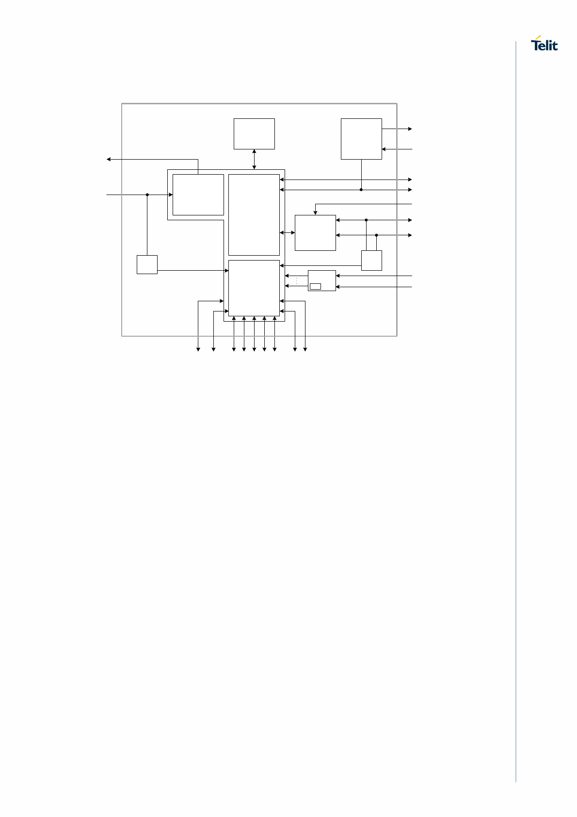
Figure 1 shows an overview of the internal architecture of the module.
It includes the following sub-functions:
• Application processor, Modem subsystem and Location processing with their
external interfaces. These three functions are contained in a single SOC.
• RF front end, including antenna diagnosis circuitry
• Analog Audio codec for attaching external speaker amplifier and microphone
• Rich IO interfaces. Depending on which of the module’s software features are
enabled, some of its interfaces that are exported through multiplexing may be used
internally and thus may not be usable by the application.
• PMIC with the RTC function inside
2
In accordance with Telit’s Robustness Validation, using AEC-Q100-defined qualification tests
LE920A4 HW User Guide General Product Description
Doc#: 1VV0301261 Block Diagram
Rev. 4.3 Page 16 of 123 2017-12-07
Figure 1: High-level Block Diagram
ANT
DIAG
Memories
RF
Frontend
GNSS Antennna
GPIO
Cellular Antenna 1
Cellular Antenna 2
Microphone
Ear / Line out
PCM In/out
SIM
GNSS_Sync
Application
Processor
Modem
Location
HSICI2C
ANT
DIAG
USB2.0SGMIISPI
UART
JTAG
Audio
CODEC
2xSDIO
PMIC VBATT
ADC
VBATT_PA
RTC

LE920A4 HW User Guide General Product Description
Doc#: 1VV0301261 Environmental Requirements
Rev. 4.3 Page 17 of 123 2017-12-07
Environmental Requirements
2.5.1. Temperature Range
Table 4: Temperature Range
Operating
temperature
range
-20 ~ +55°C
This range is defined by 3GPP (the global standard for
wireless mobile communication). Telit guarantees its modules
to comply with all the 3GPP requirements and to have full
functionality of the module with in this range.
-40 ~ +85°C
Telit guarantees full functionality within this range as well.
However, there may possibly be some performance deviations
in this extended range relative to 3GPP requirements, which
means that some RF parameters may deviate from the 3GPP
specification in the order of a few dB. For example: receiver
sensitivity or maximum output power may be slightly degraded.
Even so, all the functionalities, such as call connection, SMS,
USB communication, UART activation etc., will be maintained,
and the effect of such degradations will not lead to malfunction.
–40°C ~ +95°C
eCall must be functional (until the module is broken)
Storage and non-
operating
temperature
range
–40°C ~ +105°C
2.5.2. RoHS Compliance
As a part of Telit corporate policy of environmental protection, the module complies with
the RoHS (Restriction of Hazardous Substances) directive of the European Union (EU
directive 2011/65/EU).
LE920A4 HW User Guide General Product Description
Doc#: 1VV0301261 Frequency Bands
Rev. 4.3 Page 18 of 123 2017-12-07
Frequency Bands
The operating frequencies in GSM850, EGSM900, DCS1800, PCS1900, WCDMA & LTE
modes conform to the 3GPP specifications.
2.6.1. RF Bands per Regional Variant
Table 5 summarizes of all region variants within the module family, showing the supported
band sets in each variant.
Table 5: RF Bands per Regional Variant
Region
Variant LTE FDD LTE TDD HSPA+ TD-
SCDMA 2G
LE920A4-NA
2, 4, 5, 7, 12 - 2, 4, 5 - 2, 5
LE920A4-NV
(TBD) 2, 4, 5, 7(*), 13 - 2, 5 - -
LE920A4-EU 1, 3, 5(*), 7, 8, 20, 28(*) - 1, 3, 5(*), 8 - 3, 8
HE920A-EU
(Non-LTE,
TBD)
- - 1, 3, 5, 8 - 2, 3, 5,
8
LE920A4-CN 1, 3, 5, 8, 26 38, 39, 40, 41M 1, 5, 8 34, 39 3, 8
LE920A4-AP
(TBD) 1, 3, 5, 7, 8, 19, 21, 26,
28 - 1, 3, 5, 6, 8,
19 - 2, 3, 5,
8
NOTE:
(*) Optional bands with a different schedule than the standard configuration,
can be removed if not required
Band 41M for China: 2,555-2,655 MHz
2.6.2. Reference Table of RF Bands Characteristics
Table 6: RF Bands Characteristics
Mode Freq. Tx
(MHz)
Freq. Rx
(MHz) Channels Tx-Rx
Offset
PCS 1900 1850.2 ~
1909.8
1930.2 ~
1989.8
512 ~ 810 80 MHz
DCS 1800 1710 ~ 1785 1805 ~ 1880 512 ~ 885 95 MHz
GSM 850 824.2 ~ 848.8 869.2 ~ 893.8 128 ~ 251 45 MHz
EGSM 900 890 ~ 915 935 ~ 960 0 ~ 124 45 MHz

LE920A4 HW User Guide General Product Description
Doc#: 1VV0301261 Frequency Bands
Rev. 4.3 Page 19 of 123 2017-12-07
Mode Freq. Tx
(MHz)
Freq. Rx
(MHz) Channels Tx-Rx
Offset
880 ~ 890 925 ~ 935 975 ~ 1023 45 MHz
WCDMA 2100 – B1 1920 ~ 1980 2110 ~ 2170 Tx: 9612 ~ 9888
Rx: 10562 ~ 10838
190 MHz
WCDMA 1900 – B2 1850 ~ 1910 1930 ~ 1990 Tx: 9262 ~ 9538
Rx: 9662 ~ 9938
80 MHz
WCDMA 1800 – B3 1710 ~ 1785 1805 ~ 1880 Tx: 937 ~ 1288
Rx: 1162 ~ 1513
95 MHz
WCDMA AWS – B4 1710 ~ 1755 2110 ~ 2155 Tx: 1312 ~ 1513
Rx: 1537 ~ 1738
400 MHz
WCDMA 850 – B5 824 ~ 849 869 ~ 894 Tx: 4132 ~ 4233
Rx: 4357 ~ 4458
45 MHz
WCDMA 900 – B8 880 ~ 915 925 ~ 960 Tx: 2712 ~ 2863
Rx: 2937 ~ 3088
45 MHz
WCDMA 1800 – B9 1750 ~
1784.8
1845 ~ 1879.8 Tx: 8762 ~ 8912
Rx: 9237 ~ 9387
95 MHz
WCDMA 800 – B19 830 ~ 845 875 ~ 890 Tx: 312 ~ 363
Rx: 712 ~ 763
45 MHz
TDSCDMA 2000 –
B34
2010 ~ 2025 2010 ~ 2025 Tx: 10054 ~ 10121
Rx: 10054 ~ 10121
0 MHz
TDSCDMA 1900 –
B39
1880 ~ 1920 1880 ~ 1920 Tx: 9404 ~ 9596
Rx: 9404 ~ 9596
0 MHz
LTE 2100 – B1 1920 ~ 1980 2110 ~ 2170 Tx: 18000 ~ 18599
Rx: 0 ~ 599
190 MHz
LTE 1900 – B2 1850 ~ 1910 1930 ~ 1990 Tx: 18600 ~ 19199
Rx: 600 ~ 1199
80 MHz
LTE 1800 – B3 1710 ~ 1785 1805 ~ 1880 Tx: 19200 ~ 19949
Rx: 1200 ~ 1949
95 MHz

LE920A4 HW User Guide General Product Description
Doc#: 1VV0301261 Frequency Bands
Rev. 4.3 Page 20 of 123 2017-12-07
Mode Freq. Tx
(MHz)
Freq. Rx
(MHz) Channels Tx-Rx
Offset
LTE AWS – B4 1710 ~ 1755 2110 ~ 2155 Tx: 19950 ~ 20399
Rx: 1950 ~ 2399
400 MHz
LTE 850 – B5 824 ~ 849 869 ~ 894 Tx: 20400 ~ 20649
Rx: 2400 ~ 2649
45 MHz
LTE 2600 – B7 2500 ~ 2570 2620 ~ 2690 Tx: 20750 ~ 21449
Rx: 2750 ~ 3449
120 MHz
LTE 900 – B8 880 ~ 915 925 ~ 960 Tx: 21450 ~ 21799
Rx: 3450 ~ 3799
45 MHz
LTE 1800 – B9 1749.9 ~
1784.9
1844.9 ~
1879.9
Tx: 21800 ~ 2149
Rx: 3800 ~ 4149
95 MHz
LTE AWS+ – B10 1710 ~ 1770 2110 ~ 2170 Tx: 22150 ~ 22749
Rx: 4150 ~ 4749
400 MHz
LTE 700a – B12 699 ~ 716 729 ~ 746 Tx : 23010 ~ 23179
Rx : 5010 ~ 5179
30 MHz
LTE 700c – B13 777 ~ 787 746 ~ 756 Tx : 27210 ~ 27659
Rx : 9210 ~ 9659
-31 MHz
LTE 700b – B17 704 ~ 716 734 ~ 746 Tx: 23730 ~ 23849
Rx: 5730 ~ 5849
30 MHz
LTE 800 – B19 830 ~ 845 875 ~ 890 Tx: 24000 ~ 24149
Rx: 6000 ~ 6149
45 MHz
LTE 800 – B20 832 ~ 862 791 ~ 821 Tx: 24150 ~ 24449
Rx: 6150 ~ 6449
-41 MHz
LTE 1500 – B21 1447.9 ~
1462.9
1495.9 ~
1510.9
Tx: 24450 ~ 24599
Rx: 6450 ~ 6599
48 MHz
LTE 850+ – B26 814 ~ 849 859 ~ 894 Tx: 26690 ~ 27039
Rx: 8690 ~ 9039
45 MHz

LE920A4 HW User Guide General Product Description
Doc#: 1VV0301261 RF parameters
Rev. 4.3 Page 21 of 123 2017-12-07
Mode Freq. Tx
(MHz)
Freq. Rx
(MHz) Channels Tx-Rx
Offset
LTE 700 – B28 703 ~ 748 758 ~ 803 Tx : 27210 ~ 27659
Rx : 9210 ~ 9659
45 MHz
LTE TDD 2600 –
B38
2570 ~ 2620 2570 ~ 2620 Tx: 37750 ~ 38250
Rx: 37750 ~ 38250
0 MHz
LTE TDD 1900 –
B39
1880 ~ 1920 1880 ~ 1920 Tx: 38250 ~ 38650
Rx: 38250 ~ 38650
0 MHz
LTE TDD 2300 –
B40
2300 ~ 2400 2300 ~ 2400 Tx: 38650 ~ 39650
Rx: 38650 ~ 39650
0 MHz
LTE TDD 2500 –
B41M
2555 ~ 2655 2555 ~ 2655 Tx: 40265 ~ 41215
Rx: 40265 ~ 41215
0 MHz
RF parameters
2.7.1. Sensitivity
The module’s maximum sensitivity levels are as follows:
• -108 dBm @ 2G
• -113 dBm @ 3G
• -102 dBm @ 4G FDD (BW=5 MHz)
2.7.2. Output power
LE920A4 typical values for Max output level are as follow:
• 2G:
- LB: 33dBm
- HB: 30dBm
• 3G/TD-SCDMA: 24dBm
• 4G (FDD & TDD):23dBm @1RB.

LE920A4 HW User Guide General Product Description
Doc#: 1VV0301261 Mechanical Dimensions
Rev. 4.3 Page 22 of 123 2017-12-07
Mechanical Dimensions
The module’s overall dimensions are as follows:
• Length: 34 mm, +/- 0.15 mm tolerance
• Width: 40 mm, +/- 0.15 mm tolerance
• Thickness: 2.9 mm, +/- 0.15 mm tolerance
NOTE:
A typical label thickness of 0.11 mm should be considered in addition to the
module thickness
Weight
The nominal weight of the module is 9.0 gram.
LE920A4 HW User Guide Module Connections
Doc#: 1VV0301261 Pin-out
Rev. 4.3 Page 23 of 123 2017-12-07
3. Module Connections
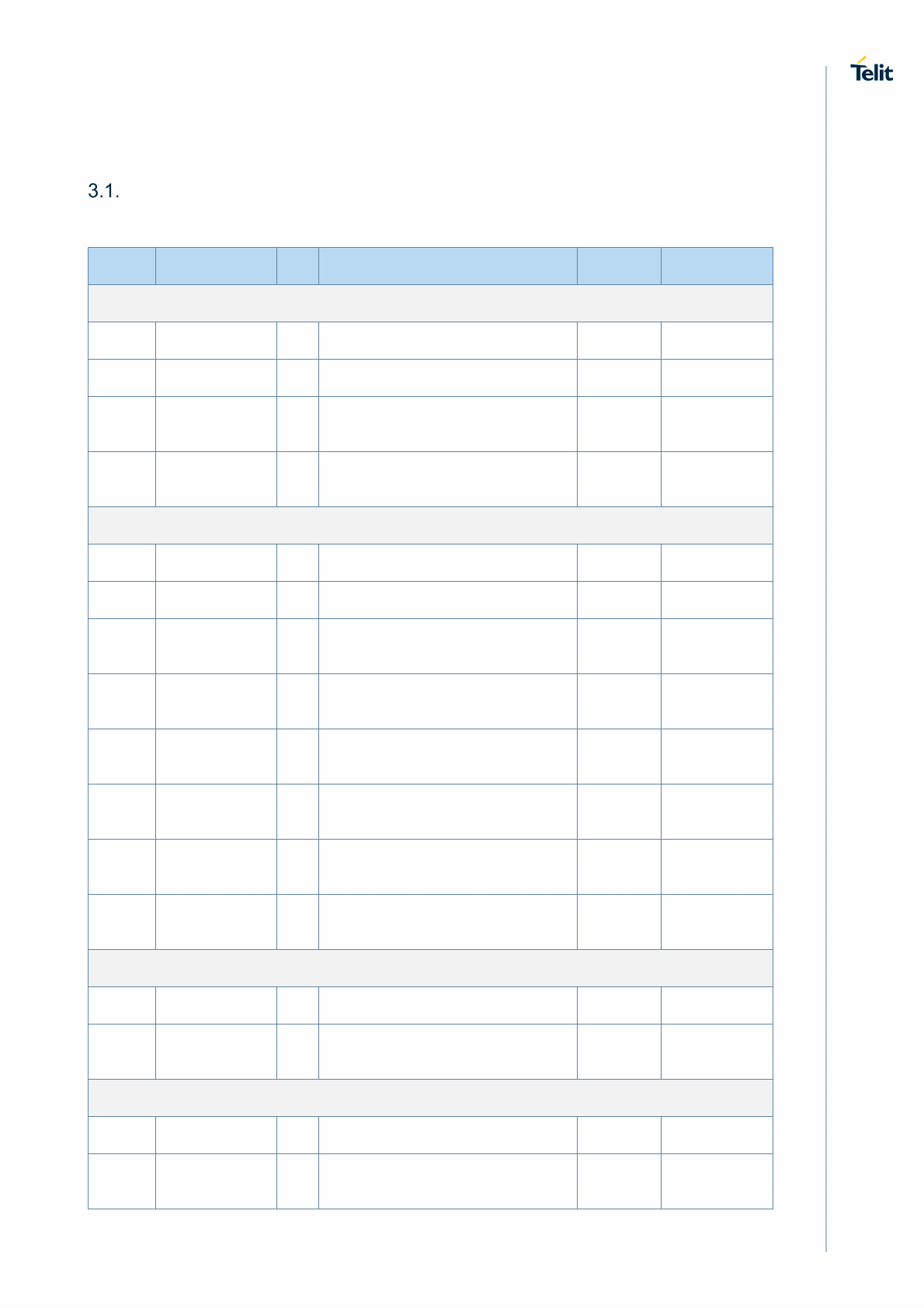
Pin-out
Table 7: Pin-out
PAD Signal I/O Function Type Comment
USB HS 2.0 Communication Port
D19 USB_D+ I/O USB differential data(+)
F19 USB_D- I/O USB differential data(-)
A18 USB_VBUS AI Power sense for the internal USB
transceiver Power
B19 USB_ID AI USB ID for supporting USB2.0
OTG
Asynchronous UART
AH19 C103/TXD I Serial data input (TXD) from DTE 1.8V
AF19 C104/RXD O Serial data output to DTE 1.8V
AA18 C105/RTS I Input for Request To Send signal
(RTS) from DTE 1.8V
AK19 C106/CTS O Output for Clear To Send signal
(CTS) to DTE 1.8V
AG18 C107/DSR O Output for Data Set Ready (DSR)
to DTE 1.8V Alternate Fn
GPIO_32
AC18 C108/DTR I Input for Data Terminal Ready
(DTR) from DTE 1.8V Alternate Fn
GPIO_34
AE18 C109/DCD O Output for Data Carrier Detect
(DCD) to DTE 1.8V Alternate Fn
GPIO_33
AJ18 C125/RING O Output for Ring Indication (RI) to
DTE 1.8V Alternate Fn
GPIO_31
Asynchronous Auxiliary UART
AB19 TX_AUX O Auxiliary UART (Tx Data to DTE) 1.8V
AD19 RX_AUX I Auxiliary UART (Rx Data from
DTE) 1.8V
SPI – Serial Peripheral Interface
P19 SPI_CLK O SPI clock output 1.8V
M19 SPI_MISO I SPI data Master Input Slave
Output 1.8V
LE920A4 HW User Guide Module Connections
Doc#: 1VV0301261 Pin-out
Rev. 4.3 Page 24 of 123 2017-12-07
PAD Signal I/O Function Type Comment
K19 SPI_MOSI O SPI data Master Output Slave
Input 1.8V
N18 SPI_CS O SPI chip select output 1.8V
SD/MMC Card Interface
AH17 SD/MMC_CM
D I/O SD command 1.8/2.95V
AD17 SD/MMC_CLK O SD card clock 1.8/2.95V
Y17 SD/MMC_DAT
A0 I/O SD Serial Data 0 1.8/2.95V
AF17 SD/MMC_DAT
A1 I/O SD Serial Data 1 1.8/2.95V
AB17 SD/MMC_DAT
A2 I/O SD Serial Data 2 1.8/2.95V
W17 SD/MMC_DAT
A3 I/O SD Serial Data 3 1.8/2.95V
U17 SD/MMC_CD I SD card detect input 1.8V Active Low
S17 VMMC - Power supply for MMC card pull-
up resistors 1.8/2.95V
WiFi (SDIO) Interface
AB3 WiFi_SD_CM
D I/O WiFi SD command 1.8V
AM3 WiFi_SD_CLK O WiFi SD clock 1.8V
AD3 WiFi_SD_DAT
A0 I/O WiFi SD Serial Data 0 1.8V
AF3 WiFi_SD_DAT
A1 I/O WiFi SD Serial Data 1 1.8V
AH3 WiFi_SD_DAT
A2 I/O WiFi SD Serial Data 2 1.8V
AK3 WiFi_SD_DAT
A3 I/O WiFi SD Serial Data 3 1.8V
Y3 WiFi_SDRST O WiFi Reset / Power enable control 1.8V Active Low
AA4 WLAN_SLEEP
_CLK O WiFi Sleep clock output 1.8V
X4 RFCLK2_QCA
O WiFi low-noise RF clock output 1.8V
LE920A4 HW User Guide Module Connections
Doc#: 1VV0301261 Pin-out
Rev. 4.3 Page 25 of 123 2017-12-07
PAD Signal I/O Function Type Comment
LTE-WiFi Coexistence
AS3 WCI_TX O Wireless coexistence interface
TXD 1.8V
AT2 WCI_RX
I Wireless coexistence interface
RXD 1.8V
SIM Card Interface 1
A10 SIMCLK1 O External SIM 1 signal – Clock 1.8/2.85V
B11 SIMRST1 O External SIM 1 signal – Reset 1.8/2.85V
B9 SIMIO1 I/O External SIM 1 signal - Data I/O 1.8/2.85V Internally PU
20 kΩ to
SIMVCC1
B7 SIMIN1 I External SIM1 signal - Presence 1.8V Active low
A8 SIMVCC1 - External SIM1 signal – power
supply for SIM1 1.8/2.85V
E8 Reserved for
ESIM_RST I Reserved for eSIM signal – Reset 1.8/2.85V
Reserved
SIM Card Interface 2
C16 SIMCLK2 O External SIM 2 signal – Clock 1.8/2.85V
D17 SIMRST2 O External SIM 2 signal – Reset 1.8/2.85V
E16 SIMIO2 I/O External SIM 2 signal – Data I/O 1.8/2.85V Internally PU
20kΩ to
SIMVCC2
C18 SIMIN2 I External SIM 2 signal – Presence 1.8V Active low
D15 SIMVCC2 - External SIM2 signal – Power
supply for SIM2 1.8/2.85V
Analog Audio interface
B5 EAR1_MT+ AO Earphone signal output1, phase + Audio
A4 EAR1_MT- AO Earphone signal output1, phase - Audio
B3 MIC1_MT+ AI Mic signal input1, phase + Audio
A2 MIC1_MT- AI Mic signal input1, phase - Audio
G6 MICBIAS AO Mic BIAS Audio
E2 EAR2_MT+ AO Earphone signal output2, phase + Audio

LE920A4 HW User Guide Module Connections
Doc#: 1VV0301261 Pin-out
Rev. 4.3 Page 26 of 123 2017-12-07
PAD Signal I/O Function Type Comment
D1 EAR2_MT- AO Earphone signal output2, phase - Audio
C2 MIC2_MT+ AI Mic signal input2, phase + Audio
B1 MIC2_MT- AI Mic signal input2, phase - Audio
Digital Voice Interface (DVI)
D11 DVI_WA0 O Digital Voice interface (WA0
master output) 1.8V
C8 DVI_RX I Digital Voice interface (Rx) 1.8V
D9 DVI_TX O Digital Voice interface (Tx) 1.8V
C10 DVI_CLK O Digital Voice interface (CLK master
output) 1.8V
C12 REF_CLK O Reference clock for external
Codec 1.8V
General Purpose Digital I/O
F9 GPIO_01 I/O GPIO_01 1.8V Alternate Fn
I2C
E10 GPIO_02 I/O GPIO_02 1.8V Alternate Fn
I2C
F11 GPIO_03 I/O GPIO_03 1.8V Alternate Fn
I2C
E12 GPIO_04 I/O GPIO_04 1.8V Alternate Fn
I2C
F13 GPIO_05 I/O GPIO_05 1.8V Alternate Fn
I2C
E14 GPIO_06 I/O GPIO_06 1.8V Alternate Fn
I2C
W19 GPIO_10 I/O GPIO_10 1.8V Alternate Fn
I2C
AN4 GPIO_20 I/O GPIO_20 1.8V
RF Section
AD1 Antenna I/O GSM/EDGE/UMTS/LTE main
antenna (50 Ohm) RF
AU9 ANT_DIV I UMTS/LTE antenna diversity input
(50 Ohm) RF
LE920A4 HW User Guide Module Connections
Doc#: 1VV0301261 Pin-out
Rev. 4.3 Page 27 of 123 2017-12-07
PAD Signal I/O Function Type Comment
GPS Section
S1 ANT_GPS I GPS antenna (50 Ohm) RF
V2 GPS_LNA_EN O Enables the external regulator for
GPS LNA 1.8V
W3 GPS_SYNC O GPS sync signal for Dead
Reckoning 1.8V
Miscellaneous Functions
AN8 RESET_N I Reset input Active low
AS1 ON_OFF_N I Power ON / Power OFF input Active low
AN12 SHDN_N I Unconditional Shutdown input Active low
P17 VAUX/PWRM
ON O Supply output for external
accessories / Power ON monitor 1.8V
D5 ADC_IN1 AI Analog/Digital Converter Input 1 Analog
E6 ADC_IN2 AI Analog/Digital Converter Input 2 Analog
F7 ADC_IN3 AI Analog/Digital Converter Input 3 Analog
AU3 STAT_LED O Status Indicator LED 1.8V
AN10 SW_RDY O Indicates that the boot sequence
has completed successfully 1.8V
SGMII Interface
ZZ11 SGMII_RX_P AI SGMII receive - plus PHY
ZZ13 SGMII_RX_M AI SGMII receive - minus PHY
ZZ15 SGMII_TX_P AO SGMII transmit - plus PHY
ZZ17 SGMII_TX_M AO SGMII transmit - minus PHY
Ethernet PHY Control Interface
G14 MAC_MDC O MAC to PHY Clock 2.85V
G12 MAC_MDIO I/O MAC to PHY Data 2.85V
G8 ETH_RST_N O Ethernet PHY Reset 2.85V
G10 ETH_INT_N I Ethernet PHY Interrupt 1.8V
LE920A4 HW User Guide Module Connections
Doc#: 1VV0301261 Pin-out
Rev. 4.3 Page 28 of 123 2017-12-07
PAD Signal I/O Function Type Comment
HSIC Interface
A14 HSIC_DATA I/O High-speed inter-chip interface -
data 1.2V
A16 HSIC_STB I/O High-speed inter-chip interface -
strobe 1.2V
I2C Interface
C14 I2C_SCL I/O I2C clock 1.8V Internal PU
2.2 kΩ to
1.8V
D13 I2C_SDA I/O I2C Data 1.8V Internal PU
2.2 kΩ to
1.8V
Power Supply
AP17 VBATT - Main Power Supply (Digital
Section) Power
AP19 VBATT - Main Power Supply (Digital
Section) Power
AR18 VBATT - Main Power Supply (Digital
Section) Power
AR20 VBATT - Main Power Supply (Digital
Section) Power
AS17 VBATT_PA - Main Power Supply (RF Section) Power
AS19 VBATT_PA - Main Power Supply (RF Section) Power
AT18 VBATT_PA - Main Power Supply (RF Section) Power
AU17 VBATT_PA - Main Power Supply (RF Section) Power
AU19 VBATT_PA - Main Power Supply (RF Section) Power
AT20 VBATT_PA - Main Power Supply (RF Section) Power
A0 GND - Ground
N0 GND Ground
R0 GND - Ground
T0 GND - Ground
V0 GND - Ground
X0 GND - Ground
LE920A4 HW User Guide Module Connections
Doc#: 1VV0301261 Pin-out
Rev. 4.3 Page 29 of 123 2017-12-07
PAD Signal I/O Function Type Comment
AA0 GND - Ground
AC0 GND - Ground
AE0 GND - Ground
AG0 GND - Ground
AJ0 GND - Ground
AL0 GND - Ground
AN0 GND - Ground
AR0 GND - Ground
AV0 GND - Ground
ZZ1 GND - Ground
F1 GND - Ground
M1 GND - Ground
P1 GND - Ground
U1 GND - Ground
W1 GND - Ground
Y1 GND - Ground
AB1 GND - Ground
AF1 GND - Ground
AH1 GND - Ground
AK1 GND - Ground
AU1 GND - Ground
N2 GND - Ground
R2 GND - Ground
T2 GND - Ground
X2 GND - Ground
AA2 GND - Ground
AC2 GND - Ground
AE2 GND - Ground

LE920A4 HW User Guide Module Connections
Doc#: 1VV0301261 Pin-out
Rev. 4.3 Page 30 of 123 2017-12-07
PAD Signal I/O Function Type Comment
AG2 GND - Ground
AJ2 GND - Ground
AL2 GND - Ground
AN2 GND - Ground
AR2 GND - Ground
D3 GND - Ground
P3 GND - Ground
AP3 GND - Ground
C4 GND - Ground
AR4 GND - Ground
AT4 GND - Ground
AP5 GND - Ground
AS5 GND - Ground
AU5 GND - Ground
A6 GND - Ground
C6 GND - Ground
AR6 GND - Ground
AT6 GND - Ground
D7 GND - Ground
AP7 GND - Ground
AS7 GND - Ground
AU7 GND - Ground
T8 GND - Ground
V8 GND - Ground
X8 GND - Ground
AA8 GND - Ground
AR8 GND - Ground
AT8 GND - Ground

LE920A4 HW User Guide Module Connections
Doc#: 1VV0301261 Pin-out
Rev. 4.3 Page 31 of 123 2017-12-07
PAD Signal I/O Function Type Comment
AV8 GND - Ground
U9 GND - Ground
W9 GND - Ground
Y9 GND - Ground
AP9 GND - Ground
AS9 GND - Ground
T10 GND - Ground
V10 GND - Ground
X10 GND - Ground
AA10 GND - Ground
AR10 GND - Ground
AT10 GND - Ground
AV10 GND - Ground
U11 GND - Ground
W11 GND - Ground
Y11 GND - Ground
AP11 GND - Ground
AS11 GND - Ground
AU11 GND - Ground
A12 GND - Ground
T12 GND - Ground
V12 GND - Ground
X12 GND - Ground
AA12 GND - Ground
AR12 GND - Ground
AT12 GND - Ground
AV12 GND - Ground
B13 GND - Ground

LE920A4 HW User Guide Module Connections
Doc#: 1VV0301261 Pin-out
Rev. 4.3 Page 32 of 123 2017-12-07
PAD Signal I/O Function Type Comment
AP13 GND - Ground
AS13 GND - Ground
AR14 GND - Ground
AT14 GND - Ground
AV14 GND - Ground
B15 GND - Ground
AP15 GND - Ground
AS15 GND - Ground
AU15 GND - Ground
AN16 GND - Ground
AR16 GND - Ground
AT16 GND - Ground
AV16 GND - Ground
B17 GND - Ground
AK17 GND - Ground
AM17 GND - Ground
E18 GND - Ground
G18 GND - Ground
T18 GND - Ground
V18 GND - Ground
X18 GND - Ground
AL18 GND - Ground
AN18 GND - Ground
AV18 GND - Ground
ZZ19 GND - Ground
H19 GND - Ground
Y19 GND - Ground
AM19 GND - Ground
LE920A4 HW User Guide Module Connections
Doc#: 1VV0301261 Pin-out
Rev. 4.3 Page 33 of 123 2017-12-07
PAD Signal I/O Function Type Comment
A20 GND - Ground
L20 GND - Ground
N20 GND - Ground
AV20 GND - Ground
Reserved
C0 Reserved - Reserved
E0 Reserved - Reserved
G0 Reserved - Reserved
J0 Reserved - Reserved
L0 Reserved - Reserved
AT0 Reserved - Reserved
K1 Reserved - Reserved
AM1 Reserved - Reserved
G2 Reserved - Reserved
J2 Reserved - Reserved
L2 Reserved - Reserved
AV2 Reserved - Reserved
ZZ3 Reserved - Reserved
F3 Reserved - Reserved
H3 Reserved - Reserved
K3 Reserved - Reserved
M3 Reserved - Reserved
S3 Reserved - Reserved
U3 Reserved - Reserved
E4 Reserved - Reserved
G4 Reserved - Reserved
J4 Reserved - Reserved
L4 Reserved - Reserved

LE920A4 HW User Guide Module Connections
Doc#: 1VV0301261 Pin-out
Rev. 4.3 Page 34 of 123 2017-12-07
PAD Signal I/O Function Type Comment
N4 Reserved - Reserved
R4 Reserved - Reserved
T4 Reserved - Reserved
V4 Reserved - Reserved
AG4 Reserved - Reserved
AJ4 Reserved - Reserved
AL4 Reserved - Reserved
AV4 Reserved - Reserved
ZZ5 Reserved - Reserved
F5 Reserved - Reserved
AM5 Reserved - Reserved
AN6 Reserved - Reserved
AV6 Reserved - Reserved
ZZ7 Reserved - Reserved
AM7 Reserved - Reserved
AP1 Reserved - Reserved for RESET_N in case
that backward compatibility to
LE920 is needed (instead of Pad
AN8)
Refer to Sec.
5.3.3,
Unconditional
Hardware
Reset
ZZ9 Reserved - Reserved
AM9 Reserved - Reserved
AM11 Reserved - Reserved
AM13 Reserved - Reserved
AU13 Reserved - Reserved
AN14 Reserved - Reserved
F15 Reserved - Reserved
AM15 Reserved - Reserved
G16 Reserved - Reserved
J16 Reserved - Reserved

LE920A4 HW User Guide Module Connections
Doc#: 1VV0301261 Pin-out
Rev. 4.3 Page 35 of 123 2017-12-07
PAD Signal I/O Function Type Comment
L16 Reserved - Reserved
N16 Reserved - Reserved
R16 Reserved - Reserved
T16 Reserved - Reserved
V16 Reserved - Reserved
X16 Reserved - Reserved
AA16 Reserved - Reserved
AC16 Reserved - Reserved
AE16 Reserved - Reserved
AG16 Reserved - Reserved
AJ16 Reserved - Reserved
AL16 Reserved - Reserved
F17 Reserved - Reserved
H17 Reserved - Reserved
K17 Reserved - Reserved
M17 Reserved - Reserved
C20 Reserved - Reserved
E20 Reserved - Reserved
G20 Reserved - Reserved
J20 Reserved - Reserved
R20 Reserved - Reserved
T20 Reserved - Reserved
V20 Reserved - Reserved
X20 Reserved - Reserved
AA20 Reserved - Reserved
AC20 Reserved - Reserved
AE20 Reserved - Reserved
AG20 Reserved - Reserved
LE920A4 HW User Guide Module Connections
Doc#: 1VV0301261 Pin-out
Rev. 4.3 Page 36 of 123 2017-12-07
PAD Signal I/O Function Type Comment
AJ20 Reserved - Reserved
AL20 Reserved - Reserved
AN20 Reserved - Reserved
R18 Reserved - Reserved
S19 Reserved - Reserved
U19 Reserved - Reserved
L18 Reserved - Reserved
J18 Reserved - Reserved
H1 Reserved - Reserved
AE4 Reserved - Reserved
AC4 Reserved - Reserved
WARNING:
GPIO_20 and WCI_RX are used as special HW flags during boot.
If they are used as GPIOs, they must be connected via a 3-state buffer to
avoid any undesirable effect during the boot.
NOTE:
When the UART signals are used as the communication port between the
Host and the Modem, RTS must be connected to GND (on the module side)
if flow control is not used.
If the UART port is not used, UART signals can be left floating.
NOTE:
Unless otherwise specified, RESERVED pins must be left unconnected
(floating).
The only exceptions are listed in the Section 3.2, Signals That Must Be
Connected.

LE920A4 HW User Guide Module Connections
Doc#: 1VV0301261 Signals That Must Be Connected
Rev. 4.3 Page 37 of 123 2017-12-07
Signals That Must Be Connected
Table 8 lists the signals that must be connected even if not used by the end application.
Table 8: Mandatory Signals
PAD Signal Notes
AP17, AP19, AR18, AR20, AS17,
AS19, AT18, AU17, AU19, AT20
VBATT &
VBATT_PA
A0, N0, R0, T0, V0, X0, AA0, AC0,
AE0, AG0, AJ0, AL0,
AN0, AR0, AV0, ZZ1, F1, M1, P1, U1,
W1, Y1, AB1, AF1,
AH1, AK1, AU1, N2, R2, T2, X2, AA2,
AC2, AE2, AG2,
AJ2, AL2, AN2, AR2, D3, P3, AP3, C4,
AR4, AT4, AP5,
AS5, AU5, A6, C6, AR6, AT6, D7, AP7,
AS7, AU7, T8, V8, X8, AA8, AR8, AT8,
AV8, U9, W9, Y9, AP9, AS9, T10, V10,
X10, AA10, AR10, AT10, AV10, U11,
W11, Y11, AP11,
AS11, AU11, A12, T12, V12, X12,
AA12, AR12, AT12,
AV12, B13, AP13, AS13, AR14, AT14,
AV14, B15, AP15,
AS15, AU15, AN16, AR16, AT16,
AV16, B17, AK17,
AM17, E18, G18, T18, V18, X18, AL18,
AN18, AV18,
ZZ19, H19, Y19, AM19, A20, L20, N20,
AV20
GND
AS1 ON/OFF Main power on off signal
AN12 SHDN_N Emergency power off
D19 USB_D+ If not used, connect to a
test point or an USB
connector
F19 USB_D- If not used, connect to a
test point or an USB
connector
A18 USB_VBUS If not used, connect to a
test point or an USB
connector

LE920A4 HW User Guide Module Connections
Doc#: 1VV0301261 Signals That Must Be Connected
Rev. 4.3 Page 38 of 123 2017-12-07
PAD Signal Notes
AH19 C103/TXD If not used, connect to a
test point
AF19 C104/RXD If not used, connect to a
test point
AA18 C105/RTS If flow control is not used,
connect to GND
AK19 C106/CTS If not used, connect to a
test point
AB19 TX_AUX If not used, connect to a
test point
AD19 RX_AUX If not used, connect to a
test point
AD1 Antenna MAIN antenna
AU9 ANT_DIV
S1 ANT_GPS
J2, L2, F3, H3, K3, E4, AN14 Reserved Connect to a test point for
Telit internal use
AN4 GPIO_20 If not used, connect to a
test point
AT2 WCI_RX If not used, connect to a
test point
AS1 ON/OFF Main power on off signal
AN12 SHDN_N Emergency power off
D19 USB_D+ If not used, connect to a
test point or an USB
connector
F19 USB_D- If not used, connect to a
test point or an USB
connector
A18 USB_VBUS If not used, connect to a
test point or an USB
connector
AK19 C106/CTS If not used, connect to a
test point

LE920A4 HW User Guide Module Connections
Doc#: 1VV0301261 Signals That Must Be Connected
Rev. 4.3 Page 39 of 123 2017-12-07
PAD Signal Notes
AB19 TX_AUX If not used, connect to a
test point
AD19 RX_AUX If not used, connect to a
test point
AD1 Antenna MAIN antenna
AU9 ANT_DIV
S1 ANT_GPS
J2, L2, F3, H3, K3, E4, AN14 Reserved Connect to a test point for
Telit internal use
AN4 GPIO_20 If not used, connect to a
test point
AT2 WCI_RX If not used, connect to a
test point
LE920A4 HW User Guide Module Connections
Doc#: 1VV0301261 LE940A4 LGA Pads Layout
Rev. 4.3 Page 40 of 123 2017-12-07
LE940A4 LGA Pads Layout
Figure 2: LGA Pads Layout
zz A B C D E F G H J K L M N P R S T U V W X Y AA AB AC AD AE AF AG AH AJ AK AL AM AN AP AR AS AT AU AV
0
GND RESERV
ED
RESERV
ED
RESERV
ED
RESERV
ED RFU GND GND GND GND GND GND GND GND GND GND GND GND GND RFU GND
1GND MIC2
_MT-
EAR2
_MT- GND TGPIO
_21
TGPI O
_22 GND GND ANT
_GPS GND GND GND GND ANT 1 GND GND GND ANT 2 RESERV
ED
ON
_OFF* GND
2MIC1
_MT-
MIC2
_MT+
EAR2
_MT+
RESERV
ED
RESERV
ED
RESERV
ED GND GND GND
GPS_
LNA
_EN
GND GND GND GND GND GND GND GND GND WCI_RX
DRFU
3RESERV
ED
MIC1
_MT+ GND RESERV
ED
RESERV
ED
RESERV
ED
JTAG_T
ORIGIN GND RESERV
ED
RESERV
ED
GPS_PP
S
WiFi
_SDRST
_TGPIO
WiFi_SD
CMD_TG
PIO14
WiFi_SD
0_TGPI
O15
WiFi_SD
1_TGPI
O16
WiFi_SD
2_TGPI
O17
WiFi_SD
3_TGPI
O18
WiFi_SD
CLK_TG
PIO19
GND WCI_TX
D
STAT
_LED
4EAR1
_MT- GND RESERV
ED
RESERV
ED
RESERV
ED RFU RFU RFU RFU RFU RFCLK2
_QCA
WLAN_S
LEEP_C
LK
I2C_SDA
_AUX
I2C_SCL
_AUX
RESERV
ED
RESERV
ED
RESERV
ED
TGPIO
_20 GND GND RFU
5RESERV
ED
EAR1
_MT+
ADC
_IN1
RESERV
ED
RESERV
ED GND GND GND
6GND GND ADC
_IN2
MIC_BIA
S
LED_DR
VGND GND RFU
7RESERV
ED SIMIN1 GND ADC
_IN3 RFU GND GND GND
8SIMVCC1 DVI_RX eSIM
RST
ETH_RS
T_N GND GND GND GND RESET_
NGND GND GND
9RESERV
ED SIMIO1 DVI
_TX
TGPIO
_01 GND GND GND RESERV
ED GND GND ANT
_DIV 1
10 SIMCLK1 DVI
_CLK
TGPIO
_02
ETH_IN_
NGND GND GND GND SW_
RDY GND GND GND
11 SGMII_R
X_P
SIM
RST1
DVI
_WAO
TGPIO
_03 GND GND GND RESERV
ED GND GND GND
12 GND REF
_CLK
TGPIO
_04
MAC_
MDIO GND GND GND GND SHDN GND GND GND
13 SGMII_R
X_M GND I2C
SDA
TGPIO
_05
RESERV
ED GND GND ANT
_DIV 2
14 HSIC_D
ATA
I2C
_SCL
TGPIO
_06
MAC_
MDC
JTAG_P
S_HOLD GND GND GND
15 SGMII_T
X_P GND SIMVCC2 HW_KE
Y
RESERV
ED GND GND GND
16 HSIC_S
TB SI MCLK2 SIMIO2 RESERV
ED
RESERV
ED
RESERV
ED
RESERV
ED
RESERV
ED
RESERV
ED
RESERV
ED
RESERV
ED
RESERV
ED
RESERV
ED
RESERV
ED
RESERV
ED
RESERV
ED
RESERV
ED GND GND GND GND
17 SGMII_T
X_M GND SIM
RST2 VRTC RESERV
ED
RESERV
ED
LED_DR
V_EN
VAUX/
PWR
MON
VMMC MMC
_CD
MMC
_DAT3
MMC
_DAT0
MMC
_DAT2
MMC
_CLK
MMC
_DAT1
MMC
_CMD GND GND VBATT VBATT
_PA
VBATT
_PA
18 USB
_VBUS SIMIN2 GND GND TGPIO_
12
TGPIO_
11
SPI
_CS*
TGPIO
_07 GND GND GND C105/
RTS*
C108/
DTR*
C109/
DCD
C107/
DSR*
C125/
RING* GND GND VBATT VBATT
_PA GND
19 GND USB_ID USB
_D+
USB
_D- GND SPI
_MOSI
SPI
_MISO
SPI
_CLK
TGPIO
_08
TGPIO
_09
TGPIO
_10 GND TX
_AUX
RX
_AUX
C104/
RXD
C103/
TXD
C106/
CTS* GND VBATT VBATT
_PA
VBATT
_PA
20
GND RESERV
ED
RESERV
ED
RESERV
ED
RESERV
ED GND GND RESERV
ED
RESERV
ED
RESERV
ED
RESERV
ED
RESERV
ED
RESERV
ED
RESERV
ED
RESERV
ED
RESERV
ED RFU RFU VBATT VBATT
_PA GND
New xE920 (34 mm X 40 mm) Form Factor Pin MAP
LE920A4 HW User Guide Electrical Specifications
Doc#: 1VV0301261 Absolute Maximum Ratings – Not Operational
Rev. 4.3 Page 41 of 123 2017-12-07
4. Electrical Specifications
Absolute Maximum Ratings – Not Operational
WARNING:
A deviation from the value ranges listed below may harm the module.
Table 9: Absolute Maximum Ratings – Not Operational
Symbol Parameter Min Max Unit
VBATT Battery supply voltage on VBATT pin -0.5 +6.0 [V]
VBATT
TRANSIENT Transient voltage on pin VBATT (< 10
ms) -0.5 +7.0 [V]
VBATT_PA Battery supply voltage on VBATT_PA
pin -0.3 +6.0 [V]
Recommended Operating Conditions
Table 10: Recommended Operating Conditions
Symbol Parameter Min Typ Max Unit
T
amb
Ambient temperature -40 +25 +85 [°C]
VBATT Battery supply voltage on
VBATT pin 3.4 3.8 4.2 [V]
VBATT_PA Battery supply voltage on
VBATT_PA pin 3.4 3.8 4.2 [V]
I
BATT_PA +
I
BATT
Peak current to be used to
dimension decoupling
capacitors on VBATT_PA
pin
- 80 2000 [mA]
Logic Level Specifications
Unless otherwise specified, all the interface circuits of the module are 1.8V CMOS logic.
Only few specific interfaces (such as USIM and SD Card) are capable of dual voltage I/O.
LE920A4 HW User Guide Electrical Specifications
Doc#: 1VV0301261 Logic Level Specifications
Rev. 4.3 Page 42 of 123 2017-12-07
The following tables show the logic level specifications used in the module’s interface
circuits. The data specified in the tables below is valid throughout all drive strengths and
the entire temperature ranges.
NOTE:
Do not connect the module’s digital logic signals directly to the OEM’s digital
logic signals with a level higher than 2.7V for 1.8V CMOS signals.
4.3.1. 1.8V Pads - Absolute Maximum Ratings
Table 11: Absolute Maximum Ratings - Not Functional
Parameter Min Max
Input level on any digital pin when on -0.3V +2.16V
Input voltage on analog pins when on -0.3V +2.16 V
4.3.2. 1.8V Standard GPIOs
Table 12: Operating Range – Interface Levels (1.8V CMOS)
Pad Parameter Min Max Unit Comment
VIH Input high level 1.25V -- [V]
VIL Input low level -- 0.6V [V]
VOH Output high level 1.4V -- [V]
VOL Output low level -- 0.45V [V]
IIL Low-level input leakage
current -1 -- [uA] No pull-up
IIH High-level input leakage
current -- +1 [uA] No pull-down
RPU Pull-up resistance 30 390 [kΩ] See Note
RPD Pull-down resistance 30 390 [kΩ] See Note
Ci Input capacitance -- 5 [pF]
LE920A4 HW User Guide Electrical Specifications
Doc#: 1VV0301261 Logic Level Specifications
Rev. 4.3 Page 43 of 123 2017-12-07
NOTE:
Pull-up and Pull-down resistance of GPIO5 is different from those mentioned
above.
GPIO5 pull resistance is specified as 10KΩ to 50KΩ.
4.3.3. 1.8V SD Card Pads
Table 13: Operating Range – SD Card Pads Working at 1.8V
Pad Parameter Min Max Unit Comment
VIH Input high level 1.27V 2V [V]
VIL Input low level -0.3V 0.58V [V]
VOH Output high level 1.4V -- [V]
VOL Output low level 0 0.45V [V]
IIL Low-level input leakage
current -2 - [uA] No pull-up
IIH High-level input leakage
current - 2 [uA] No pull-down
RPU Pull-up resistance 10 100 [kΩ]
RPD Pull-down resistance 10 100 [kΩ]
Ci Input capacitance 5 [pF]
4.3.4. 1.8V SIM Card Pads
Table 14: Operating Range – SIM Pads Working at 1.8V
Pad Parameter Min Max Unit Comment
VIH Input high level 1.35V 2V [V]
VIL Input low level -0.3V 0.43V [V]
VOH
Output high level 1.35V 1.875V [V]
VOL Output low level 0V 0.4V [V]
IIL Low-level input leakage
current -2 - [uA] No pull-up
IIH High-level input leakage
current - 2 [uA] No pull-down
LE920A4 HW User Guide Electrical Specifications
Doc#: 1VV0301261 Logic Level Specifications
Rev. 4.3 Page 44 of 123 2017-12-07
Pad Parameter Min Max Unit Comment
RPU Pull-up resistance 10 100 [kΩ]
RPD Pull-down resistance 10 100 [kΩ]
Ci Input capacitance 5 [pF]
4.3.5. Dual Voltage Pads - Absolute Maximum Ratings
Table 15: Absolute Maximum Ratings - Not Functional
Parameter Min Max
Input level on any digital pin when on -0.3V +3.6V
Input voltage on analog pins when on -0.3V +3.6 V
4.3.6. SD Card Pads @ 2.95V
Table 16: Operating Range – For SD Card Pads Operating at 2.95V
Pad Parameter Min Max Unit Comments
VIH Input high level 1.9V 3.1V [V]
VIL Input low level -0.3V 0.7V [V]
VOH Output high level 2.1V 3.05V [V]
VOL Output low level 0V 0.4V [V]
IIL Low-level input leakage
current -10 [uA] No pull-up
IIH High-level input leakage
current 10 [uA] No pull-down
RPU Pull-up resistance 10 100 [kΩ]
RPD Pull-down resistance 10 100 [kΩ]
Ci Input capacitance 5 [pF]
4.3.7. SIM Card Pads @2.95V
Table 17: Operating Range – For SIM Pads Operating at 2.95V
Pad Parameter Min Max Unit Comment
VIH Input high level 2.1V 3.1V [V]
VIL Input low level -0.3V 0.55V [V]

LE920A4 HW User Guide Electrical Specifications
Doc#: 1VV0301261 Logic Level Specifications
Rev. 4.3 Page 45 of 123 2017-12-07
Pad Parameter Min Max Unit Comment
VOH Output high level 2.25V 3.1V [V]
VOL Output low level 0V 0.4V [V]
IIL Low-level input leakage
current -10 [uA] No pull-up
IIH High-level input leakage
current 10 [uA] No pull-down
RPU Pull-up resistance 10 100 [kΩ]
RPD Pull-down resistance 10 100 [kΩ]
Ci Input capacitance 5 [pF]
LE920A4 HW User Guide Hardware Commands
Doc#: 1VV0301261 Turning on the Module
Rev. 4.3 Page 46 of 123 2017-12-07
5. Hardware Commands
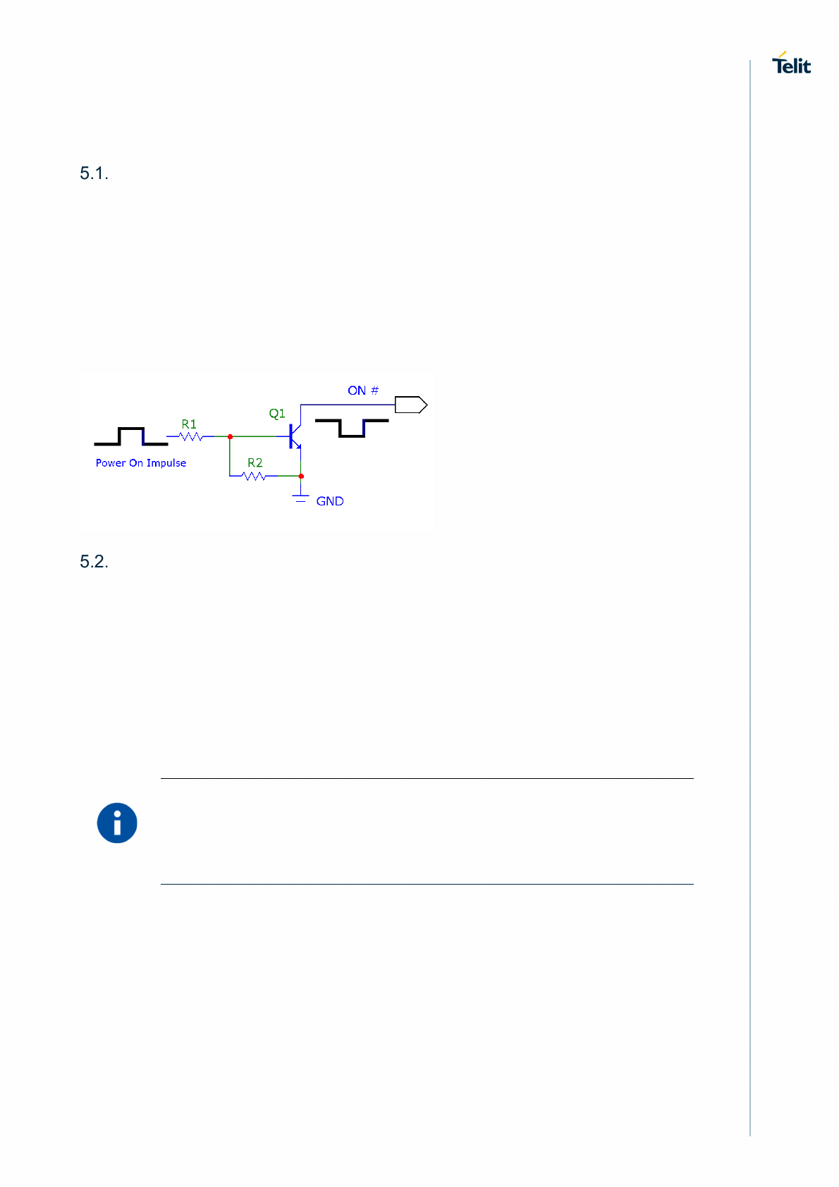
Turning on the Module
To turn on the module, the ON/OFF pad must be asserted low for at least 1 second and
then released.
The maximum current that can be drained from the ON/OFF pad is 0.1 mA. This pin is
internally pulled up; customers should expect to see ~ 800 mV on the output.
Figure 3 illustrates a simple circuit to power on the module using an inverted buffer output.
Figure 3: Power-on Circuit
Initialization and Activation State
After turning on the module, the module is not yet activated because the SW initialization
process of the module is still in process internally. It takes some time to fully complete the
HW and SW initialization of the module.
For this reason, it is impossible to access the module during the Initialization state.
As shown in Figure 4, the module becomes operational (in the Activation state) at least 20
seconds after the assertion of ON_OFF.
NOTE:
During the Initialization state, AT commands are not available. The DTE host
must wait for the Activation state prior to communicating with the module.
LE920A4 HW User Guide Hardware Commands
Doc#: 1VV0301261 Initialization and Activation State
Rev. 4.3 Page 47 of 123 2017-12-07
Figure 4: Module Initialization and Activation
NOTE:
During SW initialization of the module, the SW configures all pads and
interfaces to their desired mode. When PWRMON goes high, this indicates
that the initialization of all I/O pads is completed.
NOTE:
To check whether the module has completely powered on, monitor the
SW_RDY hardware line. When SW_RDY goes high, the module has
completely powered on and is ready to accept AT commands.
NOTE:
Do not use any pull-up resistor on the ON_OFF line as it is internally pulled
up. Using a pull-up resistor may cause latch-up problems on the module’s
power regulator and improper powering on/off of the module. The ON_OFF
line must be connected only in an open collector configuration.
NOTE:
For systems not requiring controlled power ON/OFF, automatic power on can
be supported by shorting the ON_OFF signal directly GND. In this case, the
module will start power on sequence immidiately after VBATT supply is
applied
1 Sec < T_Hold < 2 Sec
VBATT
ON_OFF
SW_RDY
T_RDY < 20 Sec
V_AUX
PWRMON
18 Sec < T_PWRMON < 20 Sec
OFF State Initialization State Active State
OK to Send AT
commands
All interfaces and pins
configured

LE920A4 HW User Guide Hardware Commands
Doc#: 1VV0301261 Turning off the Module
Rev. 4.3 Page 48 of 123 2017-12-07
NOTE:
To avoid a back-powering effect, it is recommended not to apply any HIGH
logic level signal to the digital pins of the module when it is powered OFF or
during an ON/OFF transition.
NOTE:
Active low signals are labeled with a name that ends with “_N”
Turning off the Module
Turning off the device can be done in different ways:
• AT#SHDN software command
• Hardware shutdown using ON/OFF pad
• Hardware Unconditional Shutdown using the SHDN_N
When the device is shut down by a software command or a hardware shutdown, it issues
a detach request to the network, informing the network that the device will not be
reachable any more.
NOTE:
To check if the device has powered off, monitor the PWRMON hardware
line. When PWRMON goes low, this indicates that the device has powered
off.
NOTE:
To avoid a back-powering effect, it is recommended to avoid having any
HIGH logic level signal applied to the digital pins of the module when it is
powered OFF or during an ON/OFF transition.
NOTE:
Using RESET_N for resetting the module is not recommended.
LE920A4 HW User Guide Hardware Commands
Doc#: 1VV0301261 Turning off the Module
Rev. 4.3 Page 49 of 123 2017-12-07
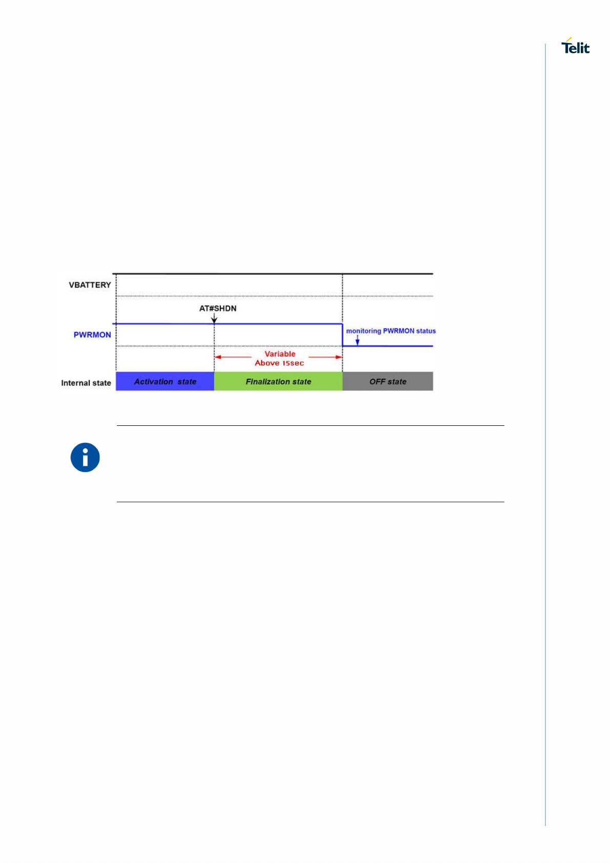
5.3.1. Shutdown by Software Command
The module can be shut down by a software command.
When a shutdown command is sent, the module goes into the Finalization state and at the
end of the finalization process shuts down PWRMON. The duration of the finalization state
can differ according to the current situation of the module, so a value cannot be defined.
Usually, it will take more than 15 seconds from sending a shutdown command until
reaching a complete shutdown. The DTE should monitor the status of PWRMON to
observe the actual power-off.
Figure 5: Shutdown by Software Command
NOTE:
To check whether the device has powered off, monitor the PWRMON
hardware line. When PWRMON goes low, the device has powered off.
5.3.2. Hardware Shutdown
To turn off the module, the ON/OFF pad must be asserted low for at least 2.5 seconds
and then released. Use the same circuitry and timing for power-on.
When the hold time of ON/OFF is above 2.5 seconds, the module goes into the
Finalization state and in the end shuts down PWRMON.
The duration of the Finalization state can differ according to the current situation of the
module, so a value cannot be defined.
Usually, it will take more than 15 seconds from sending a shutdown command until
reaching a complete shutdown. DTE should monitor the status of PWRMON to observe
the actual power-off.
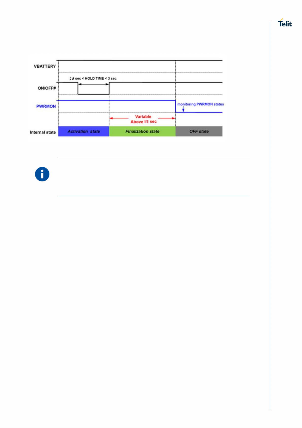
LE920A4 HW User Guide Hardware Commands
Doc#: 1VV0301261 Turning off the Module
Rev. 4.3 Page 50 of 123 2017-12-07
Figure 6: Hardware Shutdown via ON_OFF
NOTE:
To check whether the device has powered off, monitor the PWRMON
hardware line. When PWRMON goes low, the device has powered off.
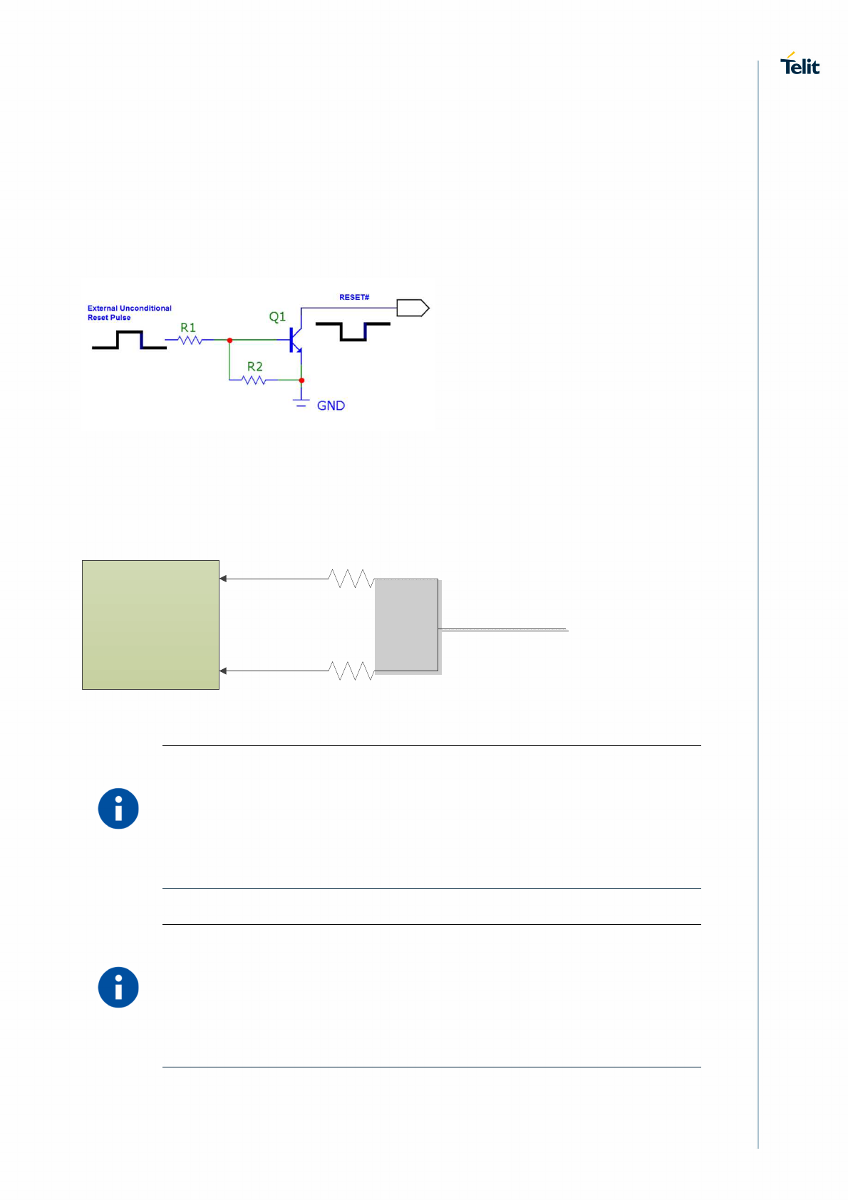
LE920A4 HW User Guide Hardware Commands
Doc#: 1VV0301261 Turning off the Module
Rev. 4.3 Page 51 of 123 2017-12-07
5.3.3. Unconditional Hardware Reset
To unconditionally restart the module, the RESET_N pad must be asserted low for a
period of 500-2000 milliseconds and then released.
Figure 7 shows a simple circuit for this action.
Figure 7: Circuit for Unconditional Hardware Reset
For keeping backward compatibility to LE920, it is recommended to prepare an alternate
connection of the RESET_N pad also to Pad AP1 while keeping Pad AN8 as the default
connection as is shown in Figure 8.
Figure 8: Alternate Connection of RESET_N Pad
LE920A4
AP1
AN8
DNP
0 Ohm
RESET#
NOTE:
In general, using RESET_N is not recommended.
The Unconditional Hardware Reset must always be implemented on the
boards, but the software must use it only as an emergency exit procedure,
and not as a normal Reset operation.
NOTE:
Do not use any pull-up resistor on the RESET_N line or any totem pole
digital output. Using a pull-up resistor may cause latch-up problems on the
module’s power regulator and improper functioning of the module. The
RESET_N line must be connected only in an open-collector configuration.
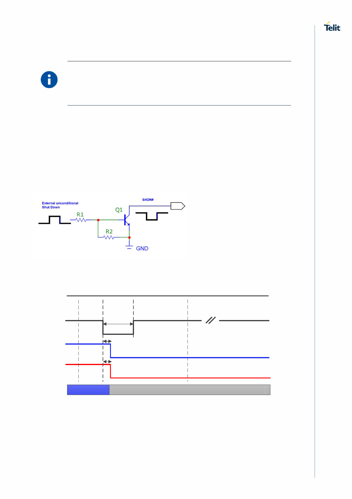
LE920A4 HW User Guide Hardware Commands
Doc#: 1VV0301261 Turning off the Module
Rev. 4.3 Page 52 of 123 2017-12-07
NOTE:
Asserting t
RESET
low for period longer than 2000 milliseconds will cause the
module to shut down.
5.3.4. Unconditional Hardware Shutdown
To unconditionally shut down the module, the SHDN_N pad must be tied low for at least
200 milliseconds and then released.
A simple circuit for applying unconditional shutdown is shown below:
Figure 9: Circuit for Unconditional Hardware Shutdown
The system power down timing for using SHDN_N is shown below
Figure 10 Power down timing using SHDN_N
200mS Sec < T_Hold
VBATT
SHDN_N
SW_RDY
T_RDY ~0 Sec
V_AUX
PWRMON
T_PWRMON ~0 Sec
OFF StateActive State

LE920A4 HW User Guide Hardware Commands
Doc#: 1VV0301261 Turning off the Module
Rev. 4.3 Page 53 of 123 2017-12-07
NOTE:
Do not use any pull-up resistor on the SHDN_N line or any totem pole digital
output. Using a pull-up resistor may cause latch-up problems on the module’s
power regulator and improper functioning of the module. The SHDN_N line
must be connected only in an open-collector configuration.
NOTE:
The Unconditional Hardware Shutdown must always be implemented on the
boards, but the software must use it only as an emergency exit procedure, and
not as a normal power-off operation.
LE920A4 HW User Guide Power Supply
Doc#: 1VV0301261 Power Supply Requirements
Rev. 4.3 Page 54 of 123 2017-12-07
6. Power Supply
The power supply circuitry and board layout are very important parts of the full product
design, with critical impact on the overall product performance. Read the following
requirements and the guidelines carefully to ensure a good and proper design.
Power Supply Requirements
The module’s power requirements are as follows:
Table 18: Power Supply Requirements
Nominal supply voltage 3.8V
Supply voltage range 3.4V – 4.2V
Max ripple on module input supply 30 mV
Table 19 provides typical current consumption values of the module for the various
available modes.
Table 19: Current Consumption
Mode Average (Typ.) Mode Description
Switched Off
Switched off 25 µA Module supplied but switched off (RTC is on)
Idle Mode (Standby Mode; No Call in Progress)
AT+CFUN=4 1.0 mA Tx and Rx disabled; module is not registered on
the network (Flight mode)
DRx GSM 2.0 mA DRx2
1.4 mA DRx5
WCDMA
1.4 mA DRx7
1.2 mA DRx8
LTE 1.8 mA Paging cycle #128 frames (1.28 sec DRx cycle)
1.4 mA Paging cycle #256 frames (2.56 sec DRx cycle)
Operative Mode (LTE)
LTE (0 dBm) 190 mA
LTE CAT 4 channel BW 20 MHz, RB=1,
Tx = 0 dBm
(Test case: BAND 1, Channel 300)
LE920A4 HW User Guide Power Supply
Doc#: 1VV0301261 Power Supply Requirements
Rev. 4.3 Page 55 of 123 2017-12-07
Mode Average (Typ.) Mode Description
LTE (22 dBm) 500 mA
LTE CAT 4 channel BW 20 MHz, RB=1,
Tx = 22 dBm
(Test case: BAND 1, Channel 300)
Operative Mode (WCDMA)
WCDMA Voice 200 mA WCDMA voice call (Tx = 10 dBm)
WCDMA
HSDPA
(0 dBm) 150 mA WCDMA data call (Cat 14, Tx = 0 dBm,
Max throughput)
WCDMA
HSDPA
(22 dBm) 310 mA WCDMA data call (Cat 14, Tx = 22 dBm,
Max throughput)
Operative Mode (GSM)
GSM Tx and Rx mode
GSM900 PL5 250 mA GSM voice call
DCS1800 PL0 170 mA
GPRS 4 Tx + 1 Rx
GSM900 PL5 430 mA GPRS Sending Data mode (CS-4)
DCS1800 PL0 340 mA
* Worst/best case depends on network configuration and is not under module control.
NOTE:
The electrical design for the power supply must ensure a peak current output
of at least 2.0A.

LE920A4 HW User Guide Power Supply
Doc#: 1VV0301261 General Design Rules
Rev. 4.3 Page 56 of 123 2017-12-07
NOTE:
In GSM/GPRS mode, RF transmission is not continuous, but is packed into
bursts at a base frequency of about 216 Hz with relative current peaks as
high as about 2.0A. Therefore, the power supply must be designed to
withstand these current peaks without big voltage drops. This means that
both the electrical design and the board layout must be designed for this
current flow.
If the layout of the PCB is not well designed, a strong noise floor is
generated on the ground. This will reflect on all the audio paths producing an
audible annoying noise at 216 Hz.
If the voltage drops during the peaks, current absorption is too high. The
device may even shut down as a consequence of the supply voltage drop.
General Design Rules
The principal guidelines for the Power Supply Design embrace three different design
steps:
• Electrical design
• Thermal design
• PCB layout
6.2.1. Electrical Design Guidelines
The electrical design of the power supply depends strongly on the power source where
this power is drained. Power sources can be distinguished by three categories:
• +5V input (typically PC internal regulator output)
• +12V input (typically automotive)
• Battery
6.2.1.1. + 5V Input Source Power Supply Design Guidelines
• The desired output for the power supply is 3.8V. So, the difference between the
input source and the desired output is not big, and therefore a linear regulator can
be used. A switching power supply is preferred to reduce power consumption.
• When using a linear regulator, a proper heat sink must be provided to dissipate the
power generated.
• A bypass low ESR capacitor of adequate capacity must be provided to cut the
current absorption peaks close to the module. A 100 μF tantalum capacitor is
usually suitable (on both VBATT and VBATT_PA together).
• Make sure that the low ESR capacitor on the power supply output (usually a
tantalum one) is rated at least 10V.
• A protection diode must be inserted close to the power input to protect the module
from power polarity inversion.
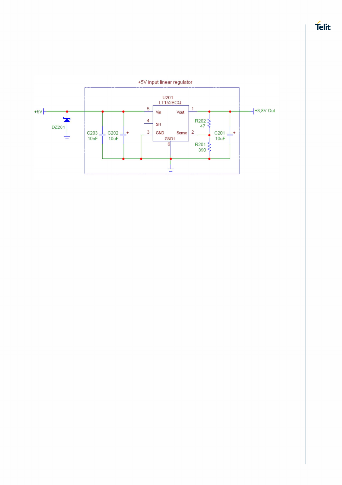
LE920A4 HW User Guide Power Supply
Doc#: 1VV0301261 General Design Rules
Rev. 4.3 Page 57 of 123 2017-12-07
Figure 11 shows an example of a linear regulator with 5V input.
Figure 11: Linear Regulator with 5V Input
6.2.1.2. + 12V Input Source Power Supply Design Guidelines
• The desired output for the power supply is 3.8V. Due to the big difference between
the input source and the desired output, a linear regulator is unsuitable and must
not be used. A switching power supply is preferable because of its better
efficiency, especially with the 2A peak current load which is expected during GSM
Tx.
• When using a switching regulator, a 500-kHz or higher switching frequency
regulator is preferable because of its smaller inductor size and its faster transient
response. This allows the regulator to respond quickly to the current peaks
absorption.
• In any case, the selection of the frequency and switching design is related to the
application to be developed due to the fact that the switching frequency can also
generate EMC interference.
• For car batteries (lead-acid accumulators) the input voltage can rise up to 15.8V.
This must be kept in mind when choosing components: all components in the
power supply must withstand this voltage.
• A bypass low ESR capacitor of adequate capacity must be provided to cut the
current absorption peaks. A 100μF tantalum capacitor is usually suitable (on both
VBATT and VBATT_PA together).
• Make sure that the low ESR capacitor on the power supply output (usually a
tantalum one) is rated at least 10V.
• For automotive applications, a spike protection diode must be inserted close to the
power input to clean the supply of spikes.
• A protection diode must be inserted close to the power input to protect the module
from power polarity inversion. This can be the same diode as for spike protection.
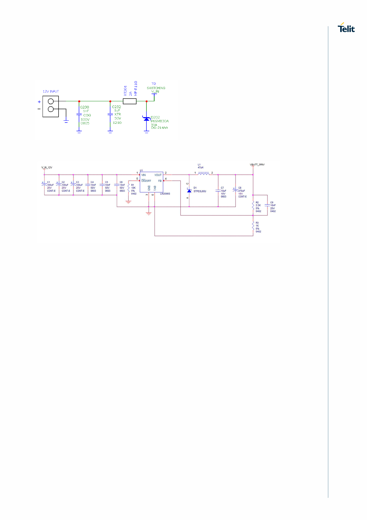
LE920A4 HW User Guide Power Supply
Doc#: 1VV0301261 General Design Rules
Rev. 4.3 Page 58 of 123 2017-12-07
Figure 12 and Figure 13 show an example of a switching regulator with 12V input.
Figure 12: Example of Switching Regulator with 12V Input – Part 1
Figure 13: Example of Switching Regulator with 12V Input – Part 2

LE920A4 HW User Guide Power Supply
Doc#: 1VV0301261 General Design Rules
Rev. 4.3 Page 59 of 123 2017-12-07
6.2.1.3. Battery Source Power Supply Design Guidelines
• The desired nominal output of the power supply is 3.8V, and the maximum allowed
voltage is 4.2V. Hence, a single 3.7V Li-Ion cell battery type is suitable for
powering the module.
WARNING:
Do not use any Ni-Cd, Ni-MH, and Pb battery types directly connected to the
module. Their use can lead to overvoltage on the module and damage it.
Use only Li-Ion battery types.
• A bypass low ESR capacitor of adequate capacity must be provided to cut the
current absorption peaks; a 100μF tantalum capacitor is usually suitable (on both
VBATT and VBATT_PA together).
• Make sure the low ESR capacitor (usually a tantalum one) is rated at least 10V.
• A protection diode must be inserted close to the power input to protect the module
from power polarity inversion. Otherwise, the battery connector must be designed
to avoid polarity inversions when connecting the battery.
• The battery capacity must be at least 500mAh to withstand the current peaks of
2A.
6.2.2. Thermal Design Guidelines
The thermal design for the power supply heat sink must be done with the following
specifications:
• Average current consumption during RF transmission @PWR level max in the
module as shown in Section 6.1, Power Supply Requirements
• Average current consumption during Class12 GPRS transmission for LE920A4-EU
and LE920A4-CN variants / Class10 GPRS transmission for LE920A4-NA @PWR
level max as shown in Section 6.1, Power Supply Requirements
• Average GPS current during GPS ON (Power Saving disabled) : mA (TBD)
NOTE:
The average consumption during transmissions depends on the power level
at which the device has to transmit via the network. The average current
consumption hence varies significantly.

LE920A4 HW User Guide Power Supply
Doc#: 1VV0301261 General Design Rules
Rev. 4.3 Page 60 of 123 2017-12-07
NOTE:
The thermal design for the power supply must be made keeping an average
consumption at the maximum transmitting level during calls of
LTE/HSPA/GPRS plus average consumption in GPS Tracking mode.
Considering the very low current during Idle, especially if the Power Saving function is
enabled, it is possible to consider from the thermal point of view that the device absorbs
significant current only during an Active Call or Data session.
For the heat generated by the module, consider it to be 2W max during transmission at
Class12 GPRS upload for LE920A4-EU and LE920A4-CN variants / Class10 GPRS
transmission for LE920A4-NA. The generated heat is mostly conducted to the ground
plane under the module. Ensure that your application can dissipate heat.
In LTE/WCDMA/HSPA mode, the module emits RF signals continuously during
transmission. Therefore, you must pay special attention how to dissipate the heat
generated.
While designing the application board, the designer must make sure that the module is
mounted on a large ground area of the application board, with many ground vias available
beneath the module for effective heat dissipation.
Even though peak current consumption in GSM mode is higher than in
LTE/WCDMA/HSPA, considerations for heat sink are more important in the case of
WCDMA due to the continuous transmission conditions.
6.2.3. Power Supply PCB Layout Guidelines
As seen in the electrical design guidelines, the power supply must have a low ESR
capacitor on the output to cut the current peaks and a protection diode on the input to
protect the supply from spikes and polarity inversion. The placement of these components
is crucial for the correct operation of the circuitry. A misplaced component can be useless
or can even decrease the power supply performances.
• The bypass low ESR capacitor must be placed close to the module power input
pads, or if the power supply is a switching type, it can be placed close to the
inductor to cut the ripple, as long as the PCB trace from the capacitor to module is
wide enough to ensure a drop-less connection even during the 2A current peaks.
• The protection diode must be placed close to the input connector where the power
source is drained.
• The PCB traces from the input connector to the power regulator IC must be wide
enough to ensure no voltage drops occur during the 2A current peaks.
Note that this is not done to save power loss but especially to avoid the voltage
drops on the power line at the current peaks frequency of 216 Hz that will reflect
on all the components connected to that supply (also introducing the noise floor at
the burst base frequency.)

LE920A4 HW User Guide Power Supply
Doc#: 1VV0301261 General Design Rules
Rev. 4.3 Page 61 of 123 2017-12-07
For this reason while a voltage drop of 300-400 mV may be acceptable from the
power loss point of view, the same voltage drop may not be acceptable from the
noise point of view. If your application does not have audio interface but only uses
the data feature of the module, this noise is not so disturbing, and the power
supply layout design can be more forgiving.
• The PCB traces to the module and to the bypass capacitor must be wide enough
to ensure that no significant voltage drops occur when the 2A current peaks are
absorbed. This is needed for the same above-mentioned reasons. Try to keep
these traces as short as possible.
• The PCB traces connecting the switching output to the inductor and the switching
diode must be kept as short as possible by placing the inductor and the diode very
close to the power switching IC (only for switching power supply). This is done to
reduce the radiated field (noise) at the switching frequency (usually 100-500 kHz).
• Use a good common ground plane.
• Place the power supply on the board in a way to guarantee that the high current
return paths in the ground plane do not overlap any noise-sensitive circuitry, such
as the microphone amplifier/buffer or earphone amplifier.
• The power supply input cables must be kept separate from noise-sensitive lines,
such as microphone/earphone cables.

LE920A4 HW User Guide Antenna(s)
Doc#: 1VV0301261 GSM/WCDMA/TD-SCDMA/LTE Antenna Requirements
Rev. 4.3 Page 62 of 123 2017-12-07
7. Antenna(s)
Antenna connection and board layout design are the most important parts in the full
product design, and they have a strong influence on the product’s overall performance.
Read carefully and follow the requirements and the guidelines for a good and proper
design.
GSM/WCDMA/TD-SCDMA/LTE Antenna Requirements
The antenna connected to the module must fulfill the following requirements:
Table 20: Antenna Requirements
Frequency range
The customer must use the most suitable antenna bandwidth
for covering the frequency bands provided by the network
operator and also supported by the car OEM while using the
Telit module.
The bands supported by each variant of the module family are
given in Section 0.
Gain Gain < 3 dBi
Impedance 50 Ohm
Input power > 33 dBm(2 W) peak power in GSM
> 24 dBm average power in WCDMA & LTE
VSWR absolute max <= 10:1
VSWR recommended <= 2:1
Since there is no antenna connector on the module, the antenna must be connected to
the module’s antenna pad (AD1) by a transmission line implemented on the PCB.
If the antenna is not directly connected to the antenna pad of the module, a PCB line is
required to connect to it or to its connector.
This transmission line must meet the following requirements:
Table 21: Antenna Line on PCB Requirements
Characteristic impedance 50 Ohm
Max attenuation 0.3 dB
Avoid coupling with other signals.

LE920A4 HW User Guide Antenna(s)
Doc#: 1VV0301261 GSM/WCDMA/TD-SCDMA/LTE Antenna – PCB Line Guidelines
Rev. 4.3 Page 63 of 123 2017-12-07
Cold End (Ground Plane) of the antenna must be equipotential to the module’s ground
pads.
Furthermore, if the device is developed for the US and/or Canada market, it must comply
with the FCC and/or IC approval requirements:
NOTE:
This device is to be used only for mobile and fixed application. The
antenna(s) used for this transmitter must be installed to provide a separation
distance of at least 20 cm from all persons and must not be co-located or
operating in conjunction with any other antenna or transmitter. End-Users
must be provided with transmitter operation conditions for satisfying RF
exposure compliance. OEM integrators must ensure that the end user has
no manual instructions to remove or install the module. Antennas used for
this module must not exceed 3dBi gain for mobile and fixed operating
configurations.
GSM/WCDMA/TD-SCDMA/LTE Antenna – PCB Line Guidelines
• Make sure that the transmission line’s characteristic impedance is 50 Ohm.
• Keep the line on the PCB as short as possible since the antenna line loss should
be less than around 0.3 dB.
• Line geometry should have uniform characteristics, constant cross section, and
avoid meanders and abrupt curves.
• Any suitable geometry/structure can be used for implementing the printed
transmission line affecting the antenna.
• If a ground plane is required in the line geometry, this plane must be continuous
and sufficiently extended so the geometry can be as similar as possible to the
related canonical model.
• Keep, if possible, at least one layer of the PCB used only for the ground plane; if
possible, use this layer as reference ground plane for the transmission line.
• Surround the PCB transmission line with ground (on both sides). Avoid having
other signal tracks facing the antenna line track directly.
• Avoid crossing any un-shielded transmission line footprint with other tracks on
different layers.
• The ground surrounding the antenna line on the PCB must be strictly connected to
the main ground plane by means of via-holes (once per 2mm at least) placed close
to the ground edges facing the line track.
• Place EM-noisy devices as far as possible from the module antenna line.
• Keep the antenna line far away from the module power supply lines.

LE920A4 HW User Guide Antenna(s)
Doc#: 1VV0301261 GSM/WCDMA/TD-SCDMA/LTE Antenna – Installation Guidelines
Rev. 4.3 Page 64 of 123 2017-12-07
• If EM-noisy devices are present on the PCB hosting the module, such as fast
switching ICs, take care to shield them with a metal frame cover.
• If EM-noisy devices are not present around the line, geometries like Micro strip or
Grounded Coplanar Waveguide are preferred because they typically ensure less
attenuation compared to a Strip line having the same length.
GSM/WCDMA/TD-SCDMA/LTE Antenna – Installation Guidelines
• Install the antenna in a location with access to the network radio signal.
• The antenna must be installed such that it provides a separation distance of at
least 20 cm from all persons and must not be co-located or operating in
conjunction with any other antenna or transmitter.
• The antenna must not be installed inside metal cases.
• The antenna must be installed according to the antenna manufacturer’s
instructions.
Antenna Diversity Requirements
This product includes an input for a second Rx antenna to improve the radio sensitivity.
The function is called Antenna Diversity.
Table 22: Antenna Diversity Requirements
Frequency range The customer must use the most suitable antenna band
width for covering the frequency bands provided by the
network operator and also supported by the car OEM while
using the Telit module.
The bands supported by each variant of the module family
are provided in Section 2.6.1, RF Bands per Regional
Variant.
Impedance 50Ω
VSWR recommended ≤ 2:1
Since there is no antenna connector on the module, the antenna must be connected to
the module’s antenna pad by a transmission line implemented on the PCB.
If the antenna is not directly connected at the antenna pad of the module, a PCB line is
required to connect to it or to its connector.
The second Rx antenna must not be located in close vicinity of the main antenna. To
improve the diversity gain and isolation and to reduce mutual interaction, the two
antennas should be located at the maximum reciprocal distance possible, taking into
consideration the available space within the application.

LE920A4 HW User Guide Antenna(s)
Doc#: 1VV0301261 GPS/GNSS Antenna Requirements
Rev. 4.3 Page 65 of 123 2017-12-07
NOTE:
If Rx Diversity is not used/connected, disable the Diversity functionality using
the AT#RXDIV or AT#LRXDIV command (refer to Ref 1: LE920A4 AT
Command User Guide) and leave the Diversity pad AU9 unconnected.
GPS/GNSS Antenna Requirements
The module supports an active antenna.
It is recommended to use antennas as follows:
• An external active antenna (17dB typ. Gain, GPS only)
• An external active antenna plus GNSS pre-filter (17dB typ. Gain)
NOTE:
The external GNSS pre-Filter is required for the GLONASS application.
The GNSS pre-filter must meet the following requirements:
• Source and load impedance = 50 Ohm
• Insertion loss (1575.42 – 1576.42 MHz) = 1.4 dB (Max)
• Insertion loss (1565.42 – 1585.42 MHz) = 2.0 dB (Max)
•
Insertion loss (1597.5515
–
1605.886
MHZ) = 2.0
dB (Max)
NOTE:
It is recommended to add a DC block to the customer’s GPS application to
prevent damage to the module due to undesired DC voltage.
NOTE:
It is recommended to add PI matching network near the GPS connector on
the application board in case that RF matching is needed.
7.5.1. Combined GPS/GNSS Antenna
The use of combined RF/GPS/GNSS antenna is NOT recommended. This solution can
generate an extremely poor GPS/GNSS reception. In addition, the combination of
antennas requires an additional diplexer, which adds significant power loss in the RF path.

LE920A4 HW User Guide Antenna(s)
Doc#: 1VV0301261 GPS/GNSS Antenna Requirements
Rev. 4.3 Page 66 of 123 2017-12-07
7.5.2. Linear and Patch GPS/GNSS Antenna
Using this type of antenna introduces at least 3 dB of loss compared to a circularly
polarized (CP) antenna. Having a spherical gain response instead of a hemispherical gain
response can aggravate the multipath behavior and create poor position accuracy.
7.5.3. Front End Design Considerations
Since there is no antenna connector on the module, the antenna must be connected to
the module through the PCB to the antenna pad.
If the antenna is not directly connected at the antenna pad of the module, a PCB line is
required. This line of transmission must meet the following requirements:
Table 23: Antenna Line on PCB Requirements
Characteristic impedance 50 Ohm
Max attenuation 0.3 dB
Avoid coupling with other signals.
Cold End (Ground Plane) of the antenna must be equipotential to the module’s ground
pads.
Furthermore, if the device is developed for the US and/or Canada market, it must comply
with the FCC and/or IC requirements.
This device is to be used only for mobile and fixed application.
7.5.4. GPS/GNSS Antenna – PCB Line Guidelines
• Ensure that the antenna line impedance is 50 Ohm.
• Keep the line on the PCB as short as possible to reduce the loss.
• The antenna line must have uniform characteristics, constant cross section, and
avoid meanders and abrupt curves.
• Keep one layer of the PCB used only for the ground plane; if possible.
• Surround (on the sides, over and under) the antenna line on the PCB with ground.
Avoid having other signal tracks directly facing the antenna line track.
• The ground around the antenna line on the PCB must be strictly connected to the
main ground plane by placing vias at least once per 2mm.
• Place EM-noisy devices as far as possible from the module antenna line.
• Keep the antenna line far away from the module power supply lines.
• If EM-noisy devices are around the PCB hosting the module, such as fast
switching ICs, ensure shielding the antenna line by burying it inside the layers of
PCB and surrounding it with ground planes; or shield it with a metal frame cover.
• If you do not have EM-noisy devices around the PCB of the module, use a Micro
strip line on the surface copper layer for the antenna line. The line attenuation will
be lower than a buried one.

LE920A4 HW User Guide Antenna(s)
Doc#: 1VV0301261 GPS/GNSS Antenna Requirements
Rev. 4.3 Page 67 of 123 2017-12-07
7.5.5. GPS/GNSS Antenna – Installation Guidelines
• The module, due to its sensitivity characteristics, is capable of performing a GNSS
localization fix inside buildings. (Still, the sensitivity could be affected by the
building characteristics, i.e. shielding.)
• The antenna must not be co-located or operating in conjunction with any other
antenna or transmitter.
• The antenna must not be installed inside metal cases.
• The antenna must be installed according to the antenna manufacturer’s
instructions.

LE920A4 HW User Guide Hardware Interfaces
Doc#: 1VV0301261 GPS/GNSS Antenna Requirements
Rev. 4.3 Page 68 of 123 2017-12-07
8. Hardware Interfaces
Table 24 summarizes all the hardware interfaces of the module.
Table 24: Hardware Interfaces
SGMII For Ethernet PHY support
Ethernet
Control
For controlling an external Ethernet PHY
HSIC x1
SDIO x2 (for SD/MMC card and for WLAN)
USB USB2.0, OTG support
SPI Master only, up to 50 MHz
I2C For sensors, audio control
UART 2 HS-UART (up to 4 Mbps)
Audio I/F I2S/PCM, Analog I/O
GPIO 8 ~ 23 (8 dedicated + 15 multiplexed with other signals)
USIM x2, dual voltage each (1.8V/2.85V)
ADC Up to x3
Antenna
ports
2 for Cellular, 1 for GNSS

LE920A4 HW User Guide Hardware Interfaces
Doc#: 1VV0301261 USB Port
Rev. 4.3 Page 69 of 123 2017-12-07
USB Port
The module includes a Universal Serial Bus (USB) transceiver, which operates at USB
high-speed (480 Mbits/sec). It can also operate with USB full-speed hosts (12 Mbits/sec).
It is compliant with the USB 2.0 specification and can be used for control and data
transfers as well as for diagnostic monitoring and firmware update.
The USB port is typically the main interface between the module and OEM hardware.
NOTE:
The USB_D+ and USB_D- signals have a clock rate of 480 MHz. The signal
traces must be routed carefully. Minimize trace lengths, number of vias, and
capacitive loading. The impedance value should be as close as possible to
90 Ohms differential.
Table 25 lists the USB interface signals.
Table 25: USB Interface Signals
Signal Pad No.
Usage
USB_VBUS A18
Power and cable detection for the internal USB transceiver.
Acceptable input voltage range 2.2V – 5.25V @ max 5 mA
consumption
USB_D- F19 Minus (-) line of the differential, bi-directional USB signal
to/from the peripheral device
USB D+ D19 Plus (+) line of the differential, bi-directional USB signal
to/from the peripheral device
USB_ID B19 USB ID signal supporting USB2.0 OTG (see note below)
NOTE:
USB_VBUS input power is internally used to detect the USB port and start
the enumeration process. A power supply pin with a maximum of 5 mA is
required.
Do not use pull up or a voltage divider for sourcing this supply
NOTE:
Even if USB communication is not used, it is still highly recommended to
place an optional USB connector on the application board.
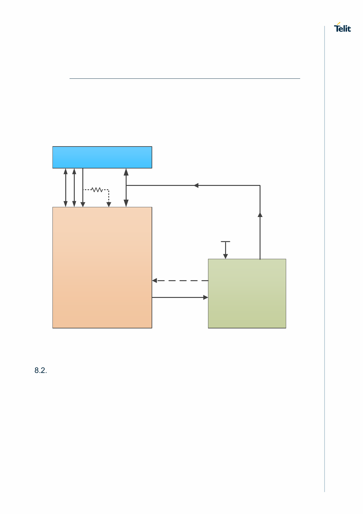
LE920A4 HW User Guide Hardware Interfaces
Doc#: 1VV0301261 HSIC Interface
Rev. 4.3 Page 70 of 123 2017-12-07
At least test points of the USB signals are required since the USB physical
communication is needed in the case of SW update.
8.1.1. USB OTG support
In order to support USB OTG, an additional 5V power supply as well as some additional
connectivity should be added externally.
The below drawing provides a high level application circuit for enabling OTG connectivity
Figure 14 OTG Connectivity
Any available USB OTG 5V Boost such as LTC3529EDCB can be used
HSIC Interface
The application processor exposes a High-Speed Inter-Chip (HSIC). HSIC eliminates the
analog transceiver from a USB interface for lower voltage operation and reduced power
dissipation. The HSIC interface is compliant with Ref 8: High-Speed Inter-Chip USB
Electrical Specification, version 1.0 (a supplement to the USB 2.0 specification, Section
3.8.2), and supports the following:
• High-speed 480 Mbps (240 MHz DDR) USB transfers are 100% host driver
compatible with traditional USB cable connected topologies
• Bidirectional data strobe signal (STROBE)
• Bidirectional data signal (DATA)
• No power consumption unless a transfer is in progress
SHDN
FAULT
VOUT
GPIOx
GPIOx
0 Ohm
LE920x4
USB Connector
USB D+
USB D-
USB ID
D19
USB ID (B19)
F19
ADC_IN1 (D5)
USB_VBUS (A18)
LTC3529EDCB
VBUS
VBATT
IDD-D+
LE920A4 HW User Guide Hardware Interfaces
Doc#: 1VV0301261 Ethernet Connectivity (optional)
Rev. 4.3 Page 71 of 123 2017-12-07
Further details will be provided in a future release of this document.
Ethernet Connectivity (optional)
Ethernet connectivity can be optionally added to LE920A4 by adding an external PHY.
PHY connectivity uses SGMII interface for Data and a few additional signals for PHY
control.
Further details can be found at Ref 8: High-Speed Inter-Chip USB Electrical Specification,
version 1.0
8.3.1. SGMII Interface
The LE920A4 module includes an integrated Ethernet MAC with an SGMII interface,
having the following key features:
• The SGMII interface can be used to connect to an external Ethernet PHY or an
external switch.
• When enabled, an additional network interface is available to the Linux kernel’s
router.
8.3.2. Ethernet Control Interface
When using an external PHY for Ethernet connectivity, the LE920A4 also includes the
control interface to manage this external PHY.
Table 26 lists the signals for controlling the external PHY.
Table 26: Ethernet Control Interface Signals
PAD
Signal I/O
Function Type COMMENT
G14 MAC_MDC O MAC to PHY Clock 2.85V
G12 MAC_MDIO I/O
MAC to PHY Data 2.85V
G8 ETH_RST_N
O Reset to Ethernet PHY 2.85V
G10 ETH_INT_N I Interrupt from Ethernet PHY 1.8V
NOTE:
The Ethernet control interface is internally (inside SoC) shared with the
USIM2 port! When Ethernet PHY is used, the USIM2 port cannot be used
(and vice versa).

LE920A4 HW User Guide Hardware Interfaces
Doc#: 1VV0301261
Rev. 4.3 Page 72 of 123 2017-12-07
NOTE:
ETH_INT_N is a 1.8V input. It has an internall pull up to 1.8V inside the
module thus it should be connected to an open drain interrupt pin of the
Ethernet PHY. In case the PHY does not support 1.8V I/O, proper level
shifter needs to be used.
Serial Ports
The serial port is typically a secondary interface between the module and OEM hardware.
Two serial ports are available on the module:
• MODEM SERIAL PORT 1(Main)
• MODEM SERIAL PORT 2 (Auxiliary)
Several configurations can be designed for the serial port on the OEM hardware. The
most common are:
• RS232 PC com port
• Microcontroller UART @ 1.8V (Universal Asynchronous Receive Transmit)
• Microcontroller UART @ 3.3V/5V or other voltages different from 1.8V
Depending on the type of serial port on the OEM hardware, a level translator circuit may
be needed to make the system operate. The only configuration that does not need level
translation is the 1.8V UART.
The levels for the module’s UART are the CMOS levels as described in Section 4.3, Logic
Level Specifications.
8.4.1. Modem Serial Port 1
Serial Port 1 is a +1.8V UART with all 8 RS232 signals.
It differs from the PC-RS232 in the signal polarity (RS232 is reversed) and levels.
Table 27 Serial Port 1 Signals
RS232
Pin
Number
Signal Pad
Number Name Usage
1 DCD -
DCD_UART
AE18 Data Carrier
Detect
Output from the module that
indicates carrier presence
2 RXD -
TX_UART AF19 Transmit line
*see Note
Output transmit line of the module
UART

LE920A4 HW User Guide Hardware Interfaces
Doc#: 1VV0301261 Serial Ports
Rev. 4.3 Page 73 of 123 2017-12-07
RS232
Pin
Number
Signal Pad
Number Name Usage
3 TXD -
RX_UART AH19 Receive line
*see Note
Input receive line of the module
UART
4 DTR -
DTR_UART
AC18 Data Terminal
Ready
Input to the module that controls
the DTE READY condition
5 GND A6, A12,
B13, 15... Ground Ground
6 DSR -
DSR_UART
AG18 Data Set
Ready
Output from the module that
indicates the module is ready
7 RTS -
RTS_UART
AA18 Request to
Send
Input to the module that controls
the Hardware flow control
8 CTS -
CTS_UART
AK19 Clear to Send
Output from the module that
controls the Hardware flow control
9 RI -
RI_UART AJ18 Ring Indicator
Output from the module that
indicates the Incoming Call
condition
NOTE:
DCD, DTR, DSR, RI signals that are not used for UART functions can be
configured as GPIO using AT commands.
NOTE:
To avoid a back-powering effect, it is recommended to avoid any HIGH logic
level signal applied to the digital pins of the module when it is powered OFF
or during an ON/OFF transition.
NOTE:
For minimum implementations, only the TXD and RXD lines must be
connected. The other lines can be left open provided a software flow control
is implemented.
LE920A4 HW User Guide Hardware Interfaces
Doc#: 1VV0301261 Serial Ports
Rev. 4.3 Page 74 of 123 2017-12-07
NOTE:
According to V.24, Rx/Tx signal names refer to the application side;
therefore, on the module side, these signal are in the opposite direction: TXD
on the application side will be connected to the receive line (here named
TXD / RX_UART) of the module serial port and vice versa for Rx.
NOTE:
Asserting the DTR pin low will prevent the UART and the entire module from
entering low power mode.
NOTE:
DTR pin can be left floating if not in use.
8.4.2. Modem Serial Port 2
Serial Port 2 is a +1.8V UART with Rx and Tx signals only.
Table 28 lists the signals of Serial Port 2.
Table 28: Modem Serial Port 2 Signals
PAD Signal I/O
Function Type Comment
AB19
TXD_AUX O Auxiliary UART (Tx Data to DTE) 1.8V
AD19
RXD_AUX
I Auxiliary UART (Rx Data to DTE) 1.8V
NOTE:
To avoid a back-powering effect, it is recommended to avoid having any
HIGH logic level signal applied to the digital pins of the module when it is
powered OFF or during an ON/OFF transition.

LE920A4 HW User Guide Hardware Interfaces
Doc#: 1VV0301261 Serial Ports
Rev. 4.3 Page 75 of 123 2017-12-07
NOTE:
The Auxiliary UART is used as the SW main debug console. It is required to
place test points on this interface even if not used.
8.4.3. RS232 Level Translation
To interface the module with a PC COM port or an RS232 (EIA/TIA-232) application, a
level translator is required. This level translator must perform the following actions:
• Invert the electrical signal in both directions
• Change the level from 0/1.8V to +15/-15V
The RS232 UART 16450, 16550, 16650 & 16750 chipsets accept signals with lower levels
on the RS232 side (EIA/TIA-562), allowing a lower voltage-multiplying ratio on the level
translator. Note that the negative signal voltage must be less than 0V and hence some
sort of level translation is always required.
The simplest way to translate the levels and invert the signal is by using a single chip-level
translator. There are a multitude of them, differing in the number of drivers and receivers
and in the levels (be sure to get a true RS232 level translator, not a RS485 or other
standards).
By convention, the driver is the level translator from the 0-1.8V UART to the RS232 level.
The receiver is the translator from the RS232 level to 0-1.8V UART.
To translate the whole set of control lines of the UART, the following is required:
• 2 drivers
• 2 receivers
NOTE:
The digital input lines operating at 1.8V CMOS have an absolute maximum
input voltage of 2.7V. The level translator IC outputs on the module side (i.e.
module inputs) will cause damage to the module inputs if the level translator
is powered by a +3.8V supply. So the level translator IC must be powered
from a dedicated +1.8V power supply.
An example of RS232 level adaption circuitry could use a MAXIM transceiver (MAX218).
In this case, the chipset is capable of translating directly from 1.8V to the RS232 levels
(Example on 4 signals only).
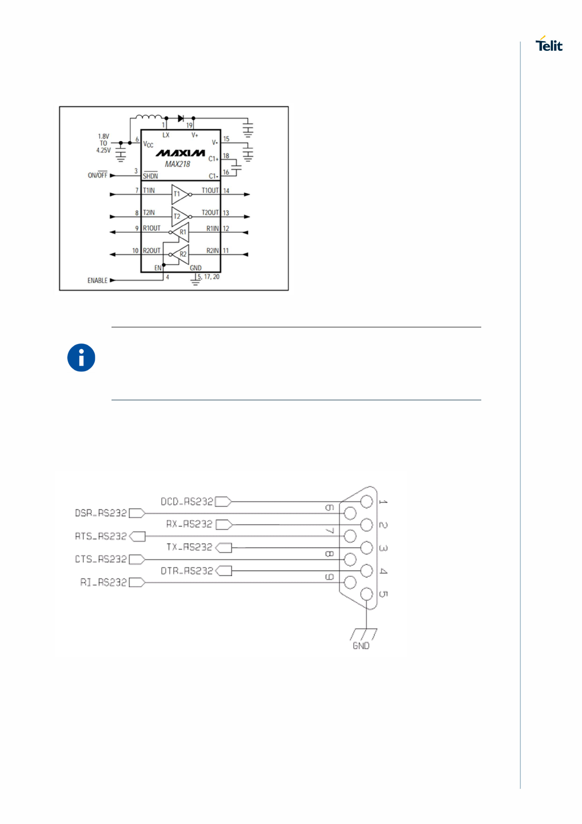
LE920A4 HW User Guide Hardware Interfaces
Doc#: 1VV0301261 Serial Ports
Rev. 4.3 Page 76 of 123 2017-12-07
Figure 15: RS232 Level Adaption Circuitry Example
NOTE:
In this case, the length of the lines on the application must be taken into
account to avoid problems in the case of High-speed rates on RS232.
The RS232 serial port lines are usually connected to a DB9 connector as shown in Figure
16. Signal names and directions are named and defined from the DTE point of view.
Figure 16: RS232 Serial Port Lines Connection Layout
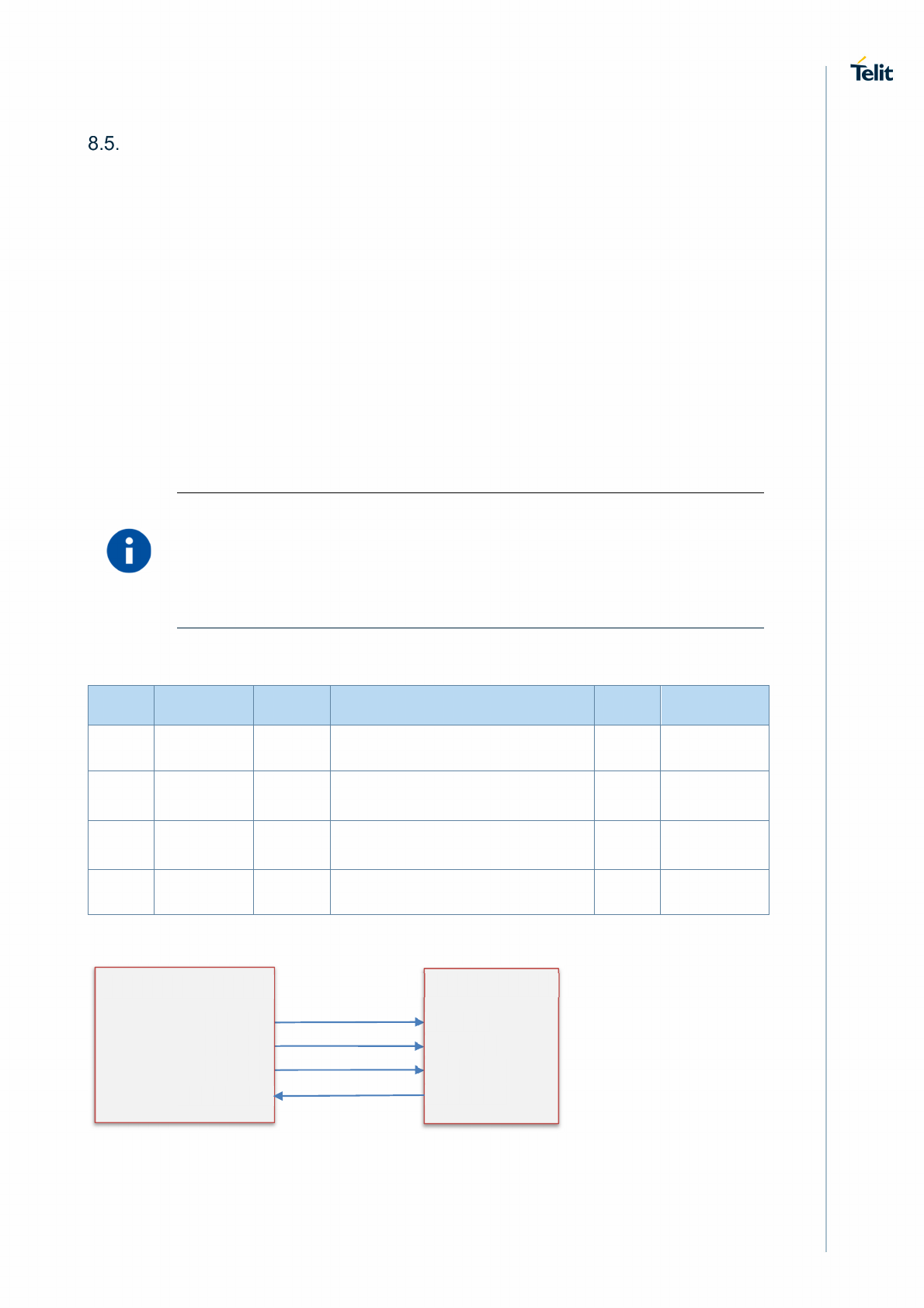
LE920A4 HW User Guide Hardware Interfaces
Doc#: 1VV0301261 Peripheral Ports
Rev. 4.3 Page 77 of 123 2017-12-07
Peripheral Ports
In addition to the serial ports, the module supports the following peripheral ports:
• SPI – Serial Peripheral Interface
• I2C – Inter-Integrated Circuit
• SD/MMC Card Interface
• SDIO Interface
8.5.1. SPI – Serial Peripheral Interface
The module’s SPI supports the following:
• Master mode only
• 1.8V CMOS level
• Up to 50 MHz clock rate
NOTE:
SPI is supported only on the Linux side.
The module supports Master mode only and cannot be configured as Slave
mode.
Table 29: SPI Signals
PAD Signal I/O Function Type Comment
P19 SPI_CLK O SPI clock output 1.8V
M19 SPI_MISO I SPI data Master input Slave
output
1.8V
K19 SPI_MOSI O SPI data Master output Slave
input
1.8V
N18 SPI_CS O SPI chip-select output 1.8V
Figure 17: SPI Signal Connectivity
Module (Master)
SPI_CS
SPI_CLK
SPI_MOSI
SPI_MISO
Host (Slave)
SPI_CS
SPI_CLK
SPI_MOSI
SPI_MISO

LE920A4 HW User Guide Hardware Interfaces
Doc#: 1VV0301261 Peripheral Ports
Rev. 4.3 Page 78 of 123 2017-12-07
8.5.2. I2C - Inter-integrated Circuit
The module supports an I2C interface on the following pins:
Table 30: I2C Signals
PAD Signal I/O Function Type Comments
C14 I2C_SCL O I2C Clock 1.8V
D13 I2C_SDA I/O I2C Data 1.8V
The I2C interface is used for controlling peripherals inside the module (such as codec,
etc.).
The I2C can also be used externally by the end customer application. However, to avoid
conflicts, the following addresses must not be used externally by the customer:
• Address 0x30 (8 bit, write), 0x31 (8 bit, read)
• Address 0x90 (8 bit, write), 0x91 (8 bit, read)
In addition, SW emulated I2C functionality can be used on GPIO 1-6 pins.
Any GPIO (among GPIO 1-6) can be configured as SCL or SDA.
The module supports I2C Master mode only.
NOTE:
SW-emulated I2C on GPIO lines is supported only from the modem side.
Refer to Ref 1: LE920A4 AT Command User Guide for command settings.
8.5.3. SD/MMC Card Interface
The module provides an SD port supporting the SD3.0 specification, which can be used to
support standard SD/MMC memory cards with the following features:
• Interface with SD/MMC memory cards up to 2 Tera Byte
• Max clock @ 2.95V - 50 MHz SDR
o Max Data: 25 MByte/s
o SD standard: HS-SDR25 at 2.95V
• Max clock @ 1.8V - 200 MHz SDR
o Max Data: 100 MByte/s
o SD standard: UHS-SDR104 at 1.8 V
• Max clock @ 1.8V - 50 MHz DDR
o Max Data: 50 MByte/s
o SD standard: UHS-DDR50 at 1.8 V
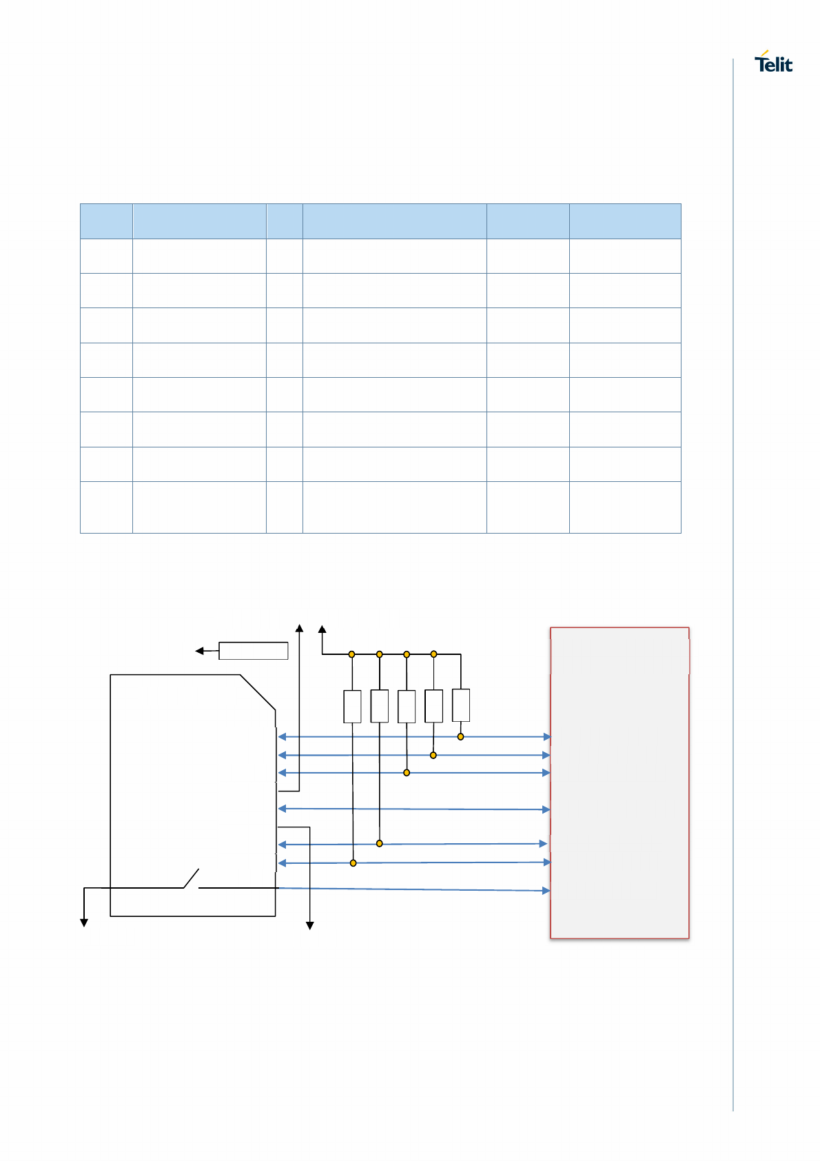
LE920A4 HW User Guide Hardware Interfaces
Doc#: 1VV0301261 Peripheral Ports
Rev. 4.3 Page 79 of 123 2017-12-07
Table 31 lists the module’s SD card signals.
Table 31: SD Card Signals
PAD Signal I/O
Function Type Comments
AH17
SD/MMC_CMD I/O
SD command 1.8/2.95V
AD17
SD/MMC_CLK O SD card clock 1.8/2.95V
Y17 SD/MMC_DATA0
I/O
SD Serial Data 0 1.8/2.95V
AF17 SD/MMC_DATA1
I/O
SD Serial Data 1 1.8/2.95V
AB17
SD/MMC_DATA2
I/O
SD Serial Data 2 1.8/2.95V
W17 SD/MMC_DATA3
I/O
SD Serial Data 3 1.8/2.95V
U17 SD/MMC_CD I SD card detect input 1.8V Active Low
S17 VMMC - Power supply for MMC
card pull-up resistors 1.8/2.95V Max Current
is 50 mA
Figure 18 shows the recommended connection diagram of the SD interface.
Figure 18: SD Interface Connectivity
SD/MMC_DATA2
SD/MMC_DATA3
SD/MMC_CMD
SD/MMC_CLK
SD/MMC_DATA0
SD/MMC_DATA1
Module
SDIO Interface
SD/MMC_CD
DATA2
DATA3
CMD
VDD
VSS
DATA0
DATA1
MicroSD
MMC_CD
GND
GND
10K
10K
10K
10K
10K
C=100nF
GND
External PS 3V VMMC
CLK
LE920A4 HW User Guide Hardware Interfaces
Doc#: 1VV0301261 Peripheral Ports
Rev. 4.3 Page 80 of 123 2017-12-07
NOTE:
SD/MMC is supported only on the Linux side.
The VMMC supply is limited to 50 mA max and can be used only to supply
the MMC card external pull-up resistors.
Pull-up resistors must be placed on the host application board.
The card detection input has an internal pull-up resistor.
NOTE:
The power supply to the SD/MMC card VCC is to be provided by the Host
application board. The module does not provide a dedicated power supply
for the SD/MMC card.
VMMC can be used to enable the external power supply (LDO Enable
signal).
8.5.4. WiFi (SDIO) Control Interface
The module provides an SDIO port supporting the SDIO3.0 specification, which can be
used to interface with a WiFi chipset (a Qualcomm QCA65x4 chipset or other WiFi
solutions - TBD)
The module includes an integrated SW driver for supporting the Qualcomm QCA65x4
chipset.
The SDIO port supports the SDIO 3.0 specification at 1.8V CMOS only, thus cannot be
used as an external SD/MMC card connection.
The module supports an LTE/WiFi coexistence mechanism via the WCI (Wireless
Coexistence Interface) port, which connects between the module and the external WiFi
IC.
For a detailed explanation, refer to Ref 6: Telit_LE920A4_LE910Cx_Wi-
Fi_Interface_Application_Note_r1.
Table 32: WiFi (SDIO) Control Interface
PAD Signal I/O Function Type Comments
AB3 WiFi_SD_CMD I/O WiFi SD Command 1.8V
AM3 WiFi_SD_CLK O WiFi SD Clock 1.8V 200 MHz
max.
AD3 WiFi_SD_DATA0 I/O WiFi SD Serial Data 0 1.8V
AF3 WiFi_SD_DATA1 I/O WiFi SD Serial Data 1 1.8V
LE920A4 HW User Guide Hardware Interfaces
Doc#: 1VV0301261 Audio Interface
Rev. 4.3 Page 81 of 123 2017-12-07
PAD Signal I/O Function Type Comments
AH3 WiFi_SD_DATA2 I/O WiFi SD Serial Data 2 1.8V
AK3 WiFi_SD_DATA3 I/O WiFi SD Serial Data 3 1.8V
Y3 WiFi_SDRST O WiFi Reset / Output Control 1.8V Active low
AS3 WCI_TX O Wireless coexistence
interface TXD 1.8V
AT2 WCI_RX I Wireless coexistence
interface RXD 1.8V
NOTE:
It is recommended that WiFi_SDRST be equipped with a pull-up resistor to
1.8V on the host application to disable the WiFi reset function if needed.
Audio Interface
The module provides analog and digital audio interfaces.
8.6.1. Analog Audio
The module provides a single analog audio path for transmitting and receiving on the
following pins:
Table 33: Analog Audio Signals
PAD Signal I/O Function Type Comment
B5 EAR1_MT+ AO Earphone Signal Output 1,
phase + Analog
A4 EAR1_MT- AO Earphone Signal Output 1,
phase - Analog
B3 MIC1_MT+ AI Mic Signal Input 1, phase + Analog
A2 MIC1_MT- AI Mic Signal Input 1, phase - Analog
G6 MICBIAS AO Mic bias Analog
E2 EAR2_MT+ AO Earphone Signal Output 2,
phase + Analog
D1 EAR2_MT- AO Earphone Signal Output 2,
phase - Analog
LE920A4 HW User Guide Hardware Interfaces
Doc#: 1VV0301261 Audio Interface
Rev. 4.3 Page 82 of 123 2017-12-07
PAD Signal I/O Function Type Comment
C2 MIC2_MT+ AI Mic Signal Input 2, phase + Analog
B1 MIC2_MT- AI Mic Signal Input 2, phase - Analog
For more details, refer to Ref 5: Digital Voice Interface_Application_Note.
WARNING:
The analog audio implementation uses an internal CODEC (inside the
module). The internal codec uses the same signals as the external digital
audio interface.
Therefore, applications that use analog audio (that is, the codec inside the
module) must make sure that the digital audio interface is either not
connected, set to Hi-Z, or set to ‘input’ to Host application.
8.6.2. Analog Audio Characteristics
The tables below list the analog audio characteristics of the audio codec included in the
module.
8.6.2.1. Analog Inputs Characteristics
Table 34: Microphone Input Characteristics (Valid for both MIC1 and MIC2)
Parameter Conditions Min Typ Max
Input
impedance 30 kΩ 50 kΩ
Max
microphone
input
Mic Digital Gain = 0dB
Mic Analog Gain = 1dBf = 1 kHz
Differential mode
450mV
P-P
THD + N Mic Gain = 0dB
f = 1 kHz
Mic Input = 1V
P-P,
Differential
mode
-80 dB
Table 35: MIC Bias Specification (Pin G6)
Parameter Conditions Min Typ Max
Voltage Load = 1 mA 1.5V 1.525V 1.55V
Max current 2 mA

LE920A4 HW User Guide Hardware Interfaces
Doc#: 1VV0301261 Audio Interface
Rev. 4.3 Page 83 of 123 2017-12-07
Parameter Conditions Min Typ Max
PSRR @217 Hz 85 dB
@10 kHz 81 dB

LE920A4 HW User Guide Hardware Interfaces
Doc#: 1VV0301261 Audio Interface
Rev. 4.3 Page 84 of 123 2017-12-07
8.6.2.2. Analog Output Characteristics
Table 36: EAR Output Characteristics (Valid for both EAR1 and EAR2)
Parameter Conditions Min Typ Max
Output impedance 16Ω 32Ω
Max power output THD < 1%
f = 1 kHz
Differential mode, R
L
= 16Ω
30 mW 52 mW
Max power output THD < 1%
f = 1 kHz
Differential mode, R
L
= 32Ω
32 mW
Full-scale output
Differential mode 1 V
RMS
Single-ended mode 0.56
V
RMS
THD+N
P
OUT
= 25 mW
R
L
= 32Ω
f = 1 kHz
Differential mode
- 80 dB
P
OUT
= 25 mW
R
L
= 32Ω
f = 1 kHz
Single-ended mode
-76 dB
LE920A4 HW User Guide Hardware Interfaces
Doc#: 1VV0301261 Audio Interface
Rev. 4.3 Page 85 of 123 2017-12-07
8.6.3. Digital Audio
The module can be connected to an external codec through the digital interface.
The product provides a single Digital Audio Interface (DVI) on the following pins:
Table 37: Digital Audio Interface (DVI) Signals
PAD
Signal I/O Function Type COMMENT
D11 DVI_WA0 O Digital Audio Interface
(WA0) B-PD 1.8V PCM_SYNC/I2S WS
C8 DVI_RX I Digital Audio Interface
(RX) B-PD 1.8V PCM_DIN/I2S_DATA_
IN
D9 DVI_TX O Digital Audio Interface
(TX) B-PD 1.8V PCM_DOUT/I2S_DAT
A_OUT
C10 DVI_CLK O Digital Audio Interface
(CLK) B-PD 1.8V PCM_CLK/I2S_CLK
C12 REF_CLK O Codec Reference
Clock B-PD 1.8V I2S_MCLK
The DVI of the module has the following characteristics:
• PCM Master mode using short or long frame sync modes
• 16 bit linear PCM format
• PCM clock rates of 256 kHz, 512 kHz, 1024 kHz and 2048 kHz (Default)
• Frame size of 8, 16, 32, 64, 128 & 256 bits per frame
• Sample rates of 8 kHz and 16 kHz
In addition to the DVI port, the module provides a master clock signal (REF_CLK on Pin
C12) which can either provide a reference clock to an external codec or form an I2S
interface together with the DVI port where the REF_CLK acts as the I2S_MCLK.
The REF_CLK default frequency is 12.288 MHz.
When using the DVI with REF_CLK as an I2S interface, 12.288 MHz is 256 x fs (where fs
= 48 kHz).
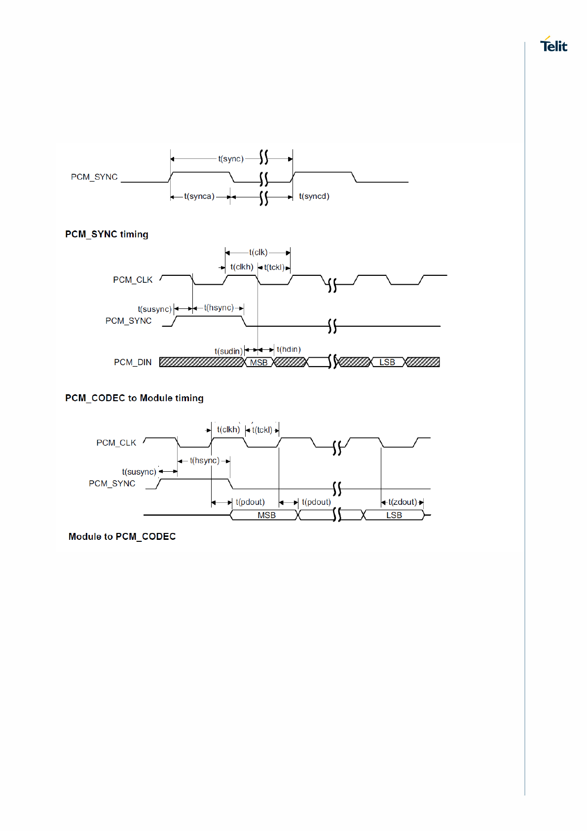
LE920A4 HW User Guide Hardware Interfaces
Doc#: 1VV0301261 Audio Interface
Rev. 4.3 Page 86 of 123 2017-12-07
8.6.3.1. Short Frame Timing Diagrams
Figure 19: Primary PCM Timing
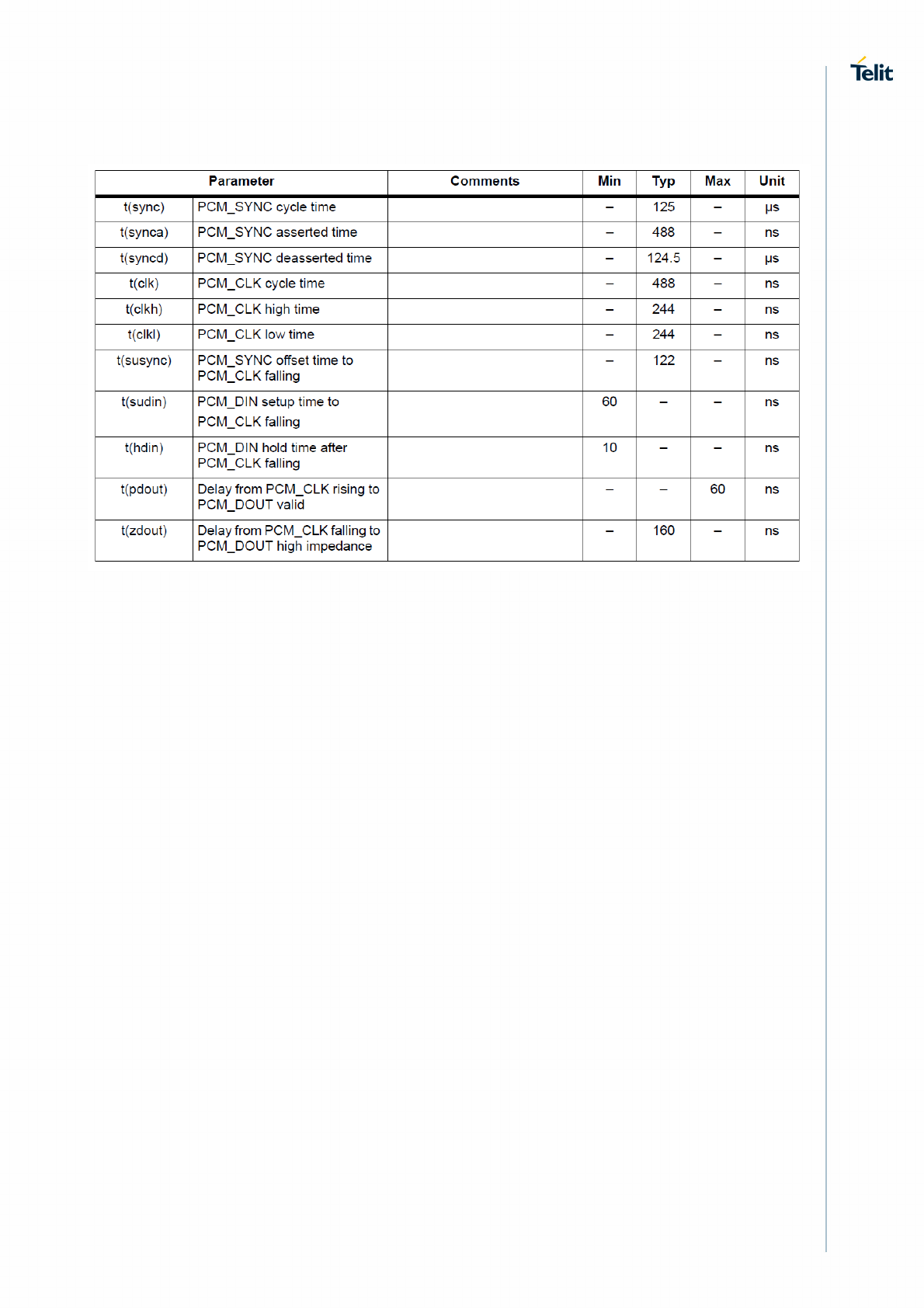
LE920A4 HW User Guide Hardware Interfaces
Doc#: 1VV0301261 Audio Interface
Rev. 4.3 Page 87 of 123 2017-12-07
Table 38: PCM_CODEC Timing Parameters
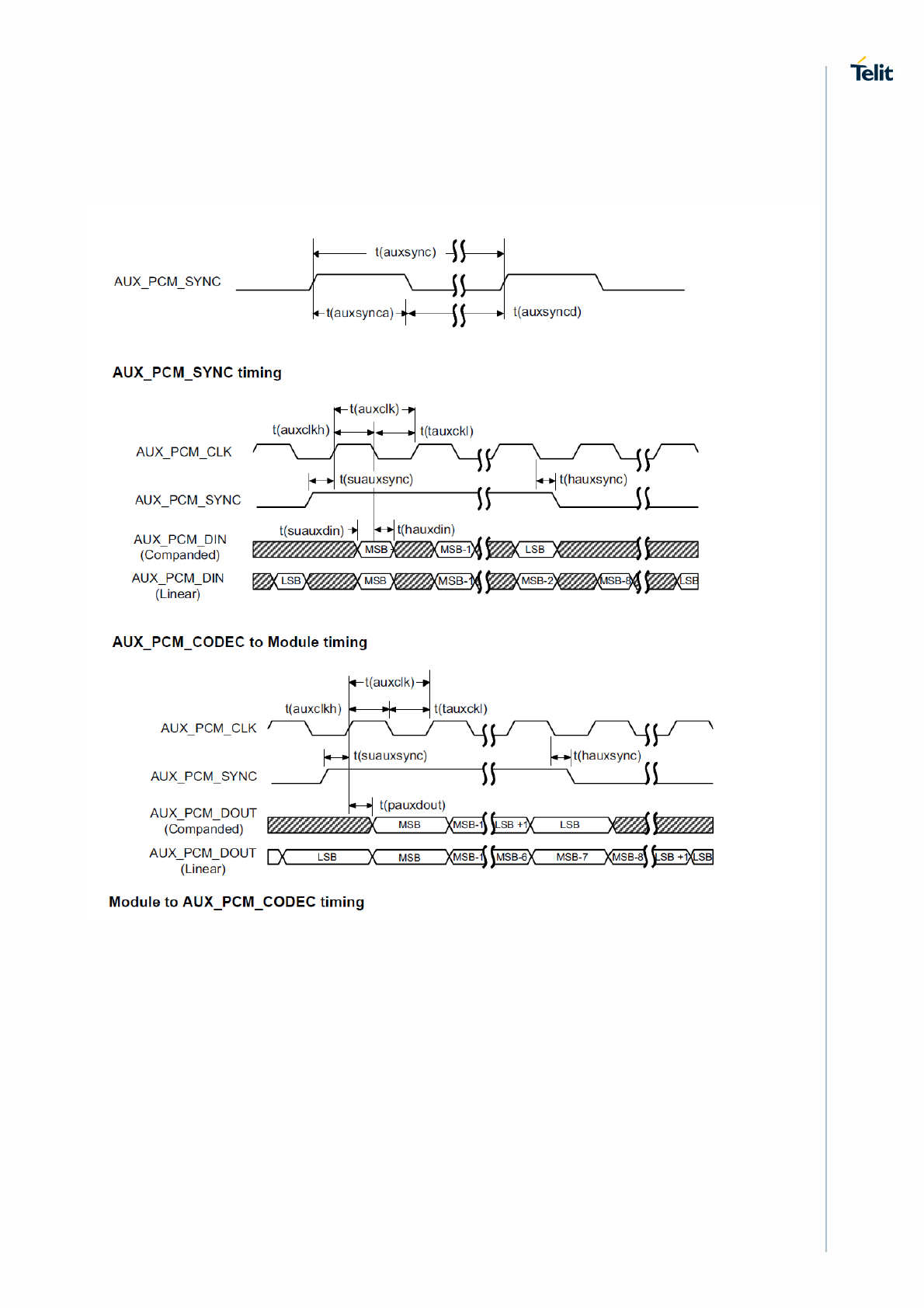
LE920A4 HW User Guide Hardware Interfaces
Doc#: 1VV0301261 Audio Interface
Rev. 4.3 Page 88 of 123 2017-12-07
8.6.3.2. Long Frame Timing Diagrams
Figure 20: Auxiliary PCM Timing
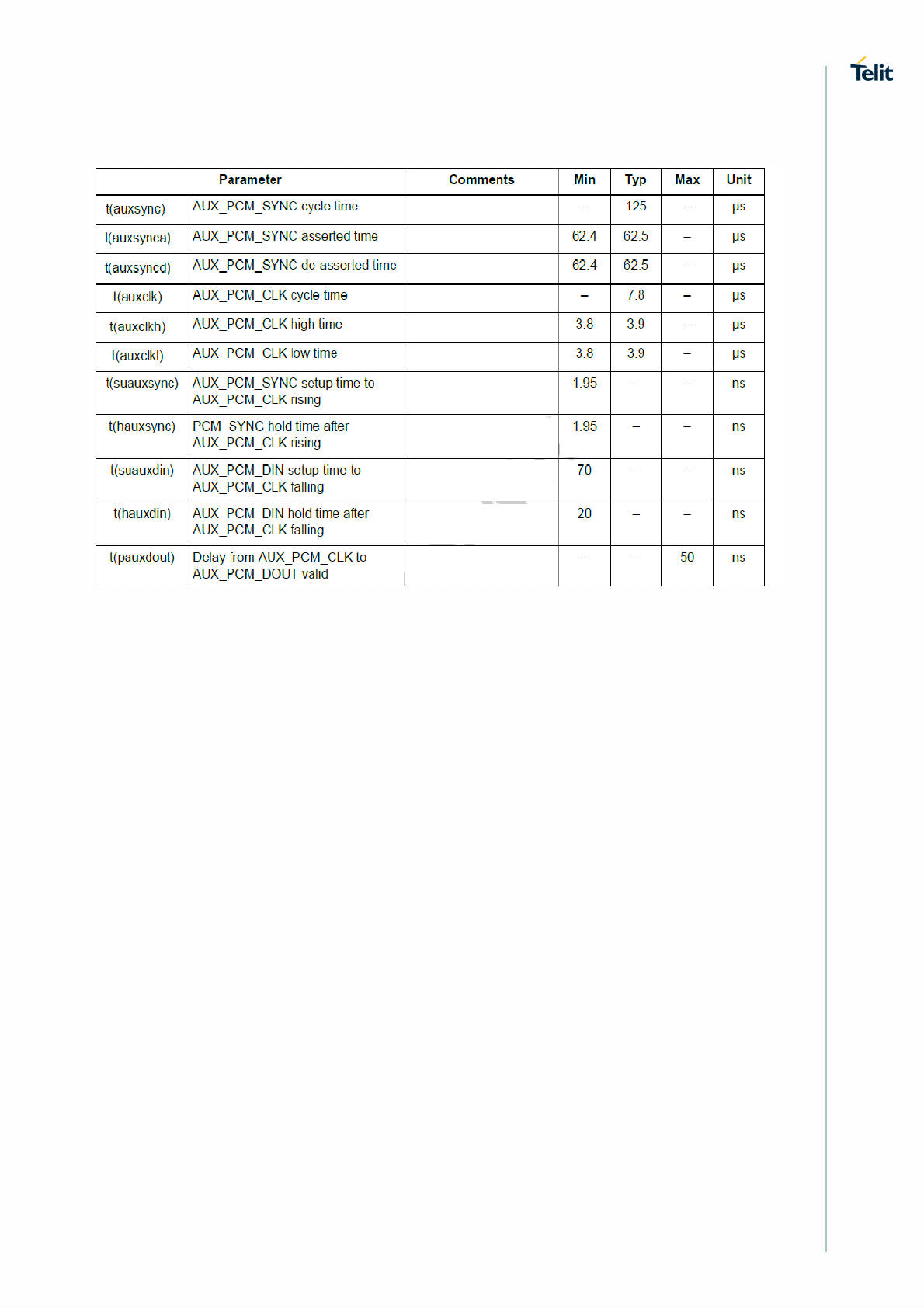
LE920A4 HW User Guide Hardware Interfaces
Doc#: 1VV0301261 Audio Interface
Rev. 4.3 Page 89 of 123 2017-12-07
Table 39: AUX_PCM_CODEC Timing Parameters
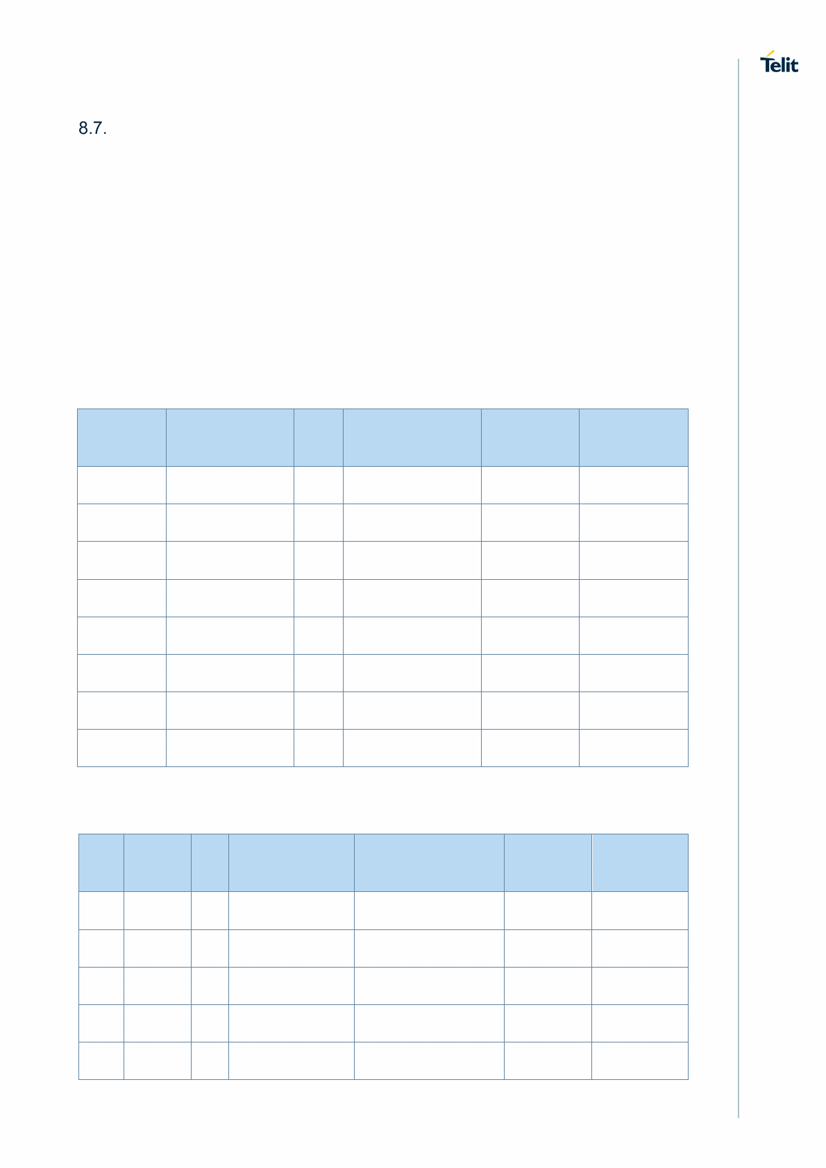
LE920A4 HW User Guide Hardware Interfaces
Doc#: 1VV0301261 General Purpose I/O
Rev. 4.3 Page 90 of 123 2017-12-07
General Purpose I/O
The general-purpose I/O pads can be configured to act in three different ways:
• Input
• Output
• Alternate function (internally controlled)
Input pads can only be read and report digital values (high or low) present on the pad at
reading time. Output pads can only be written to or queried and set the value of the pad
output. An alternate function pad is internally controlled by the module’s firmware and acts
depending on the implemented function.
The following GPIOs are available as a primary function in the module.
Table 40: Primary GPIOs
PAD Signal I/O Function Type Drive
Strength
F9 GPIO_01 I/O Configurable GPIO
CMOS 1.8V 2-16 mA
E10 GPIO_02 I/O Configurable GPIO
CMOS 1.8V 2-16 mA
F11 GPIO_03 I/O Configurable GPIO
CMOS 1.8V 2-16 mA
E12 GPIO_04 I/O Configurable GPIO
CMOS 1.8V 2-16 mA
F13 GPIO_05 I/O Configurable GPIO
CMOS 1.8V 2-16 mA
E14 GPIO_06 I/O Configurable GPIO
CMOS 1.8V 2-16 mA
W19 GPIO_10 I/O Configurable GPIO
CMOS 1.8V 2-16 mA
AN4 GPIO_20 I/O Configurable GPIO
CMOS 1.8V 2-16 mA
The additional signals below can be used as GPIOs if their initial functionality is not used.
Table 41: Additional GPIOs
PAD
Signal I/O
Initial Function
Alternate Function
Type Drive
Strength
Y3 GPIO_13
I/O WIFI_SDRST Configurable GPIO CMOS 1.8V
2-16 mA
AB3 GPIO_14
I/O WIFI_SDIO_CMD
Configurable GPIO CMOS 1.8V
2-16 mA
AD3 GPIO_15
I/O WIFI_SDIO_D0 Configurable GPIO CMOS 1.8V
2-16 mA
AF3 GPIO_16
I/O WIFI_SDIO_D1 Configurable GPIO CMOS 1.8V
2-16 mA
AH3 GPIO_17
I/O WIFI_SDIO_D2 Configurable GPIO CMOS 1.8V
2-16 mA
LE920A4 HW User Guide Hardware Interfaces
Doc#: 1VV0301261 General Purpose I/O
Rev. 4.3 Page 91 of 123 2017-12-07
PAD
Signal I/O
Initial Function
Alternate Function
Type Drive
Strength
AK3 GPIO_18
I/O WIFI_SDIO_D3 Configurable GPIO CMOS 1.8V
2-16 mA
AM3 GPIO_19
I/O WIFI_SDIO_CLK
Configurable GPIO CMOS 1.8V
2-16 mA
AJ18
GPIO_31
I/O UART_RI Configurable GPIO CMOS 1.8V
2-16 mA
AG18
GPIO_32
I/O UART_DSR Configurable GPIO CMOS 1.8V
2-16 mA
AE18
GPIO_33
I/O UART_DCD Configurable GPIO CMOS 1.8V
2-16 mA
AC18
GPIO_34
I/O UART_DTR Configurable GPIO CMOS 1.8V
2-16 mA
P19 GPIO_35
I/O SPI_CLK Configurable GPIO CMOS 1.8V
2-16 mA
M19 GPIO_36
I/O SPI_MISO Configurable GPIO CMOS 1.8V
2-16 mA
K19 GPIO_37
I/O SPI_MOSI Configurable GPIO CMOS 1.8V
2-16 mA
N18 GPIO_38
I/O SPI_CS Configurable GPIO CMOS 1.8V
2-16 mA
NOTE:
To avoid a back-powering effect, it is recommended to avoid having any
HIGH logic level signal applied to the digital pins of the module when it is
powered OFF or during an ON/OFF transition.
NOTE:
The GPIOs can also be used as alternate I2C function. Refer to Section
8.5.2, I2C - Inter-integrated Circuit.
8.7.1. Using a GPIO Pad as Input
GPIO pads, when used as inputs, can be connected to a digital output of another device
and report its status, provided this device has interface levels compatible with the 1.8V
CMOS levels of the GPIO.
If the digital output of the device is connected with the GPIO input, the pad has interface
levels different from the 1.8V CMOS. It can be buffered with an open collector transistor
with a 47 kΩ pull-up resistor to 1.8V.
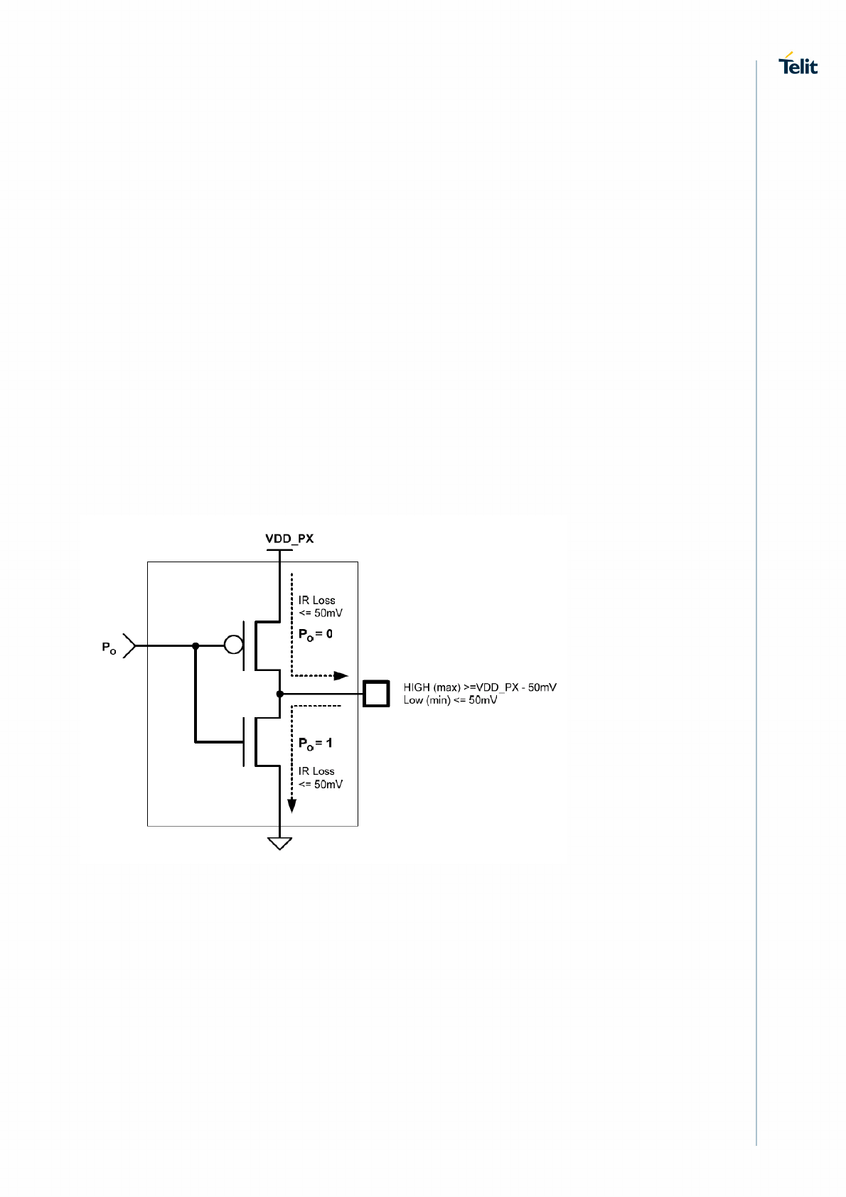
LE920A4 HW User Guide Hardware Interfaces
Doc#: 1VV0301261 General Purpose I/O
Rev. 4.3 Page 92 of 123 2017-12-07
8.7.2. Using a GPIO Pad as an Interrupt Source
GPIO pads, when used as inputs, can also be used as an interrupt source for the
software.
In general, all GPIO pads can also be used as interrupt sources. However, not all GPIOs
can be used as a wakeup source of the module (wakeup from sleep)
Only the following GPIOs can be used to wake up the system from sleep:
• GPIO1
• GPIO4
• GPIO5
8.7.3. Using a GPIO Pad as Output
GPIO pads, when used as outputs, can drive 1.8V CMOS digital devices or compatible
hardware. When set as outputs, the pads have a push-pull output, and therefore the pull-
up resistor can be omitted.
Figure 21: Output PAD Equivalent Circuit
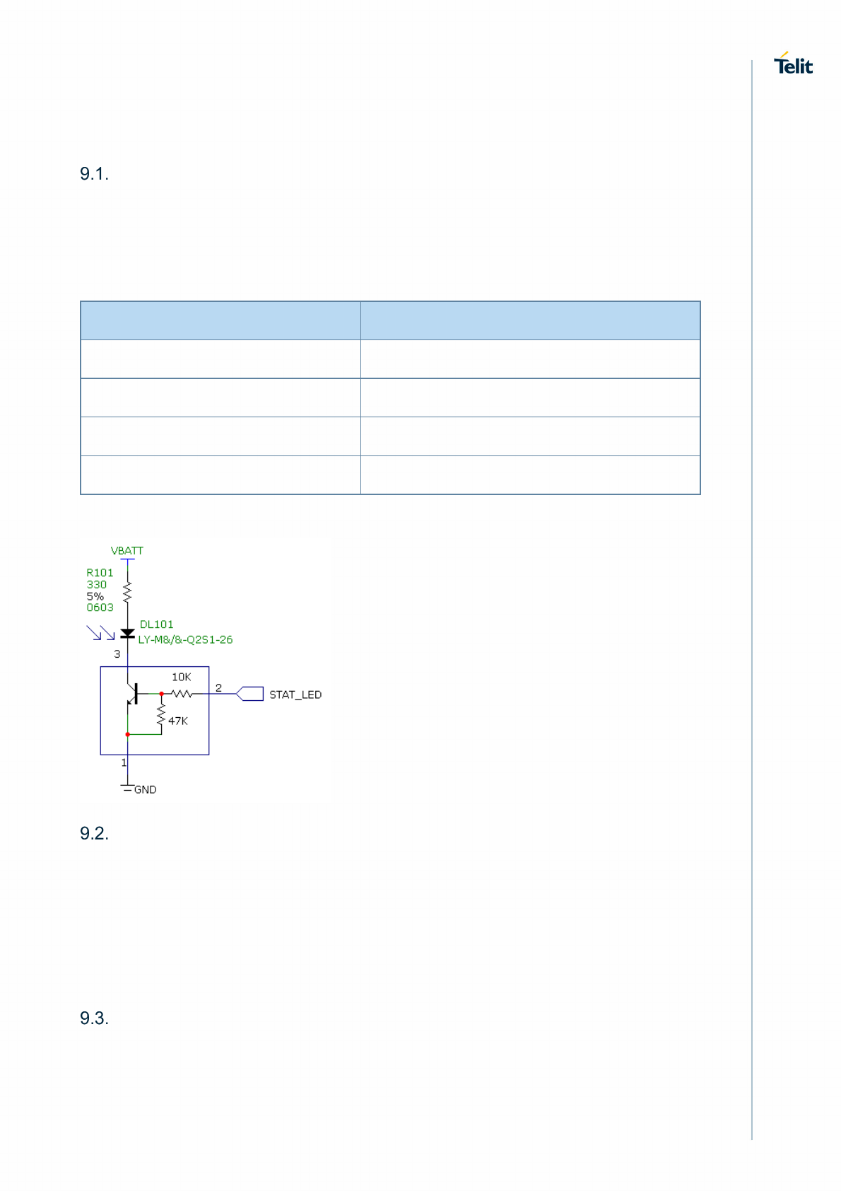
LE920A4 HW User Guide Miscellaneous Functions
Doc#: 1VV0301261 Indication of Network Service Availability
Rev. 4.3 Page 93 of 123 2017-12-07
9. Miscellaneous Functions
Indication of Network Service Availability
The STAT_LED pin status shows information on the network service availability and call
status. In the module, the STAT_LED usually needs an external transistor to drive an
external LED. Table 42 shows the device status corresponding to the pin status:
Table 42: Network Service Availability Indication
LED Status Device Status
Permanently off Device off
Fast blinking (Period 1s, T
on
0,5s) Net search / Not registered / Turning off
Slow blinking (Period 3s, T
on
0,3s) Registered full service
Permanently on A call is active
Figure 22: Status LED Reference Circuit
RTC – Real Time Clock
The RTC within the module does not have a dedicated RTC supply pin. The RTC block is
supplied by the VBATT supply.
If the battery is removed, the RTC function is not maintained. Therefore, VBATT must be
supplied continuously for maintaining the internal RTC function.
In Power OFF mode, the average current consumption is ~25 uA.
VAUX Power Output
A regulated power supply output is provided to supply power to small devices from the
module. This output is active when the module is ON and goes OFF when the module is
shut down. The operating range characteristics of the supply are as follows:

LE920A4 HW User Guide Miscellaneous Functions
Doc#: 1VV0301261 VAUX Power Output
Rev. 4.3 Page 94 of 123 2017-12-07
Table 43: Operating Range – VAUX Power Supply
Min Typical Max
Output voltage 1.75V 1.80V 1.85V
Output current 100 mA
Output bypass capacitor (inside the module) 1 μF
LE920A4 HW User Guide Miscellaneous Functions
Doc#: 1VV0301261 ADC Converter
Rev. 4.3 Page 95 of 123 2017-12-07
ADC Converter
9.4.1. Description
The module provides three 8-bit Analog to Digital converters. Each ADC reads the voltage
level applied on the relevant pin, converts it, and stores it into an 8-bit word.
Table 44 shows the ADC characteristics.
Table 44: ADC Parameters
Min Max Units
Input voltage range 0.1 1.7 Volt
AD conversion - 8 bits
Resolution - 7 mV
9.4.2. Using ADC Converter
An AT command is available to use the ADC function.
The command is AT#ADC=1,2. The read value is expressed in mV.
Refer to Ref 1: LE920A4 AT Command User Guide for the full description of this function.
Using the Temperature Monitor Function
The Temperature Monitor permits to control the module’s internal temperature and, if
properly set (see the #TEMPMON command in Ref 1: LE920A4 AT Command User
Guide), raises a GPIO to High Logic level when the maximum temperature is reached.
Fuel Gauge (optional)
The module can optionally support an external Fuel Gauge solution.
In this case, an external IC that is capable of measuring the current flow in and out of the
module must be added on the carrier board.
Figure 23 shows an example of a typical connectivity of such an external fuel gauge to the
module.
Detailed design - TBD
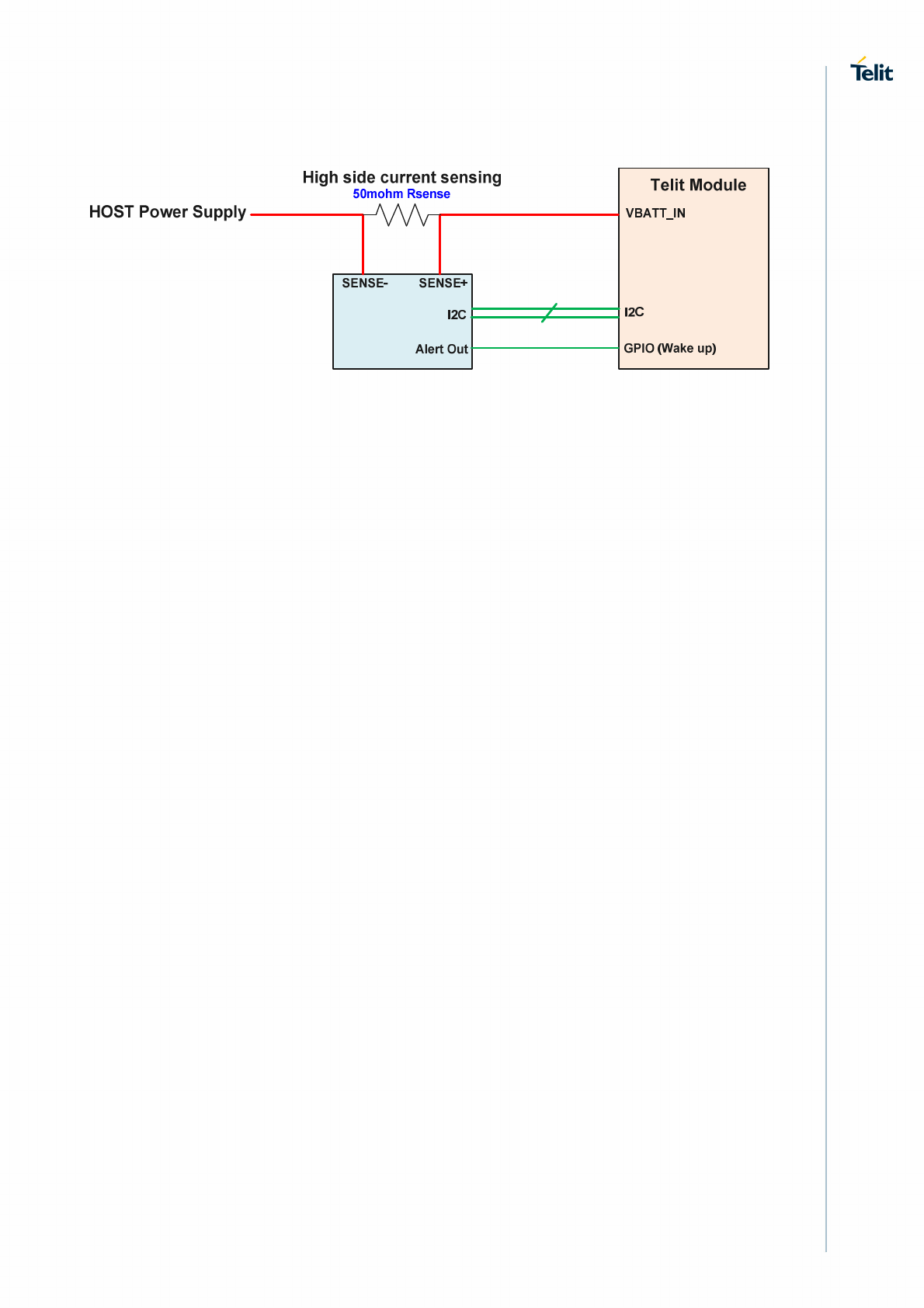
LE920A4 HW User Guide Miscellaneous Functions
Doc#: 1VV0301261 Fuel Gauge (optional)
Rev. 4.3 Page 96 of 123 2017-12-07
Figure 23: Fuel Gauge Connectivity Example

LE920A4 HW User Guide Miscellaneous Functions
Doc#: 1VV0301261 GNSS Characteristics
Rev. 4.3 Page 97 of 123 2017-12-07
GNSS Characteristics
Table 45 specifies the typical GNSS characteristics and expected performance. The
values reflect typical environment and conditions.
Table 45: GNSS Characteristics
Parameters Typical
Measurement Notes
Sensitivity
Standalone or MS-based
tracking sensitivity -162.3 dBm
Acquisition -162.3 dBm
Cold start sensitivity -157.5 dBm
TTFF
Hot 1.1s GPS+GLONASS Simulator
test
Warm 22.1s GPS+GLONASS Simulator
test
Cold 29.94s GPS+GLONASS Simulator
test
Accuracy 0.8m GPS+GLONASS Simulator
test
Min navigation update rate 1 Hz
Dynamics 2g
Operation limits 515 m/sec
A-GPS Supported
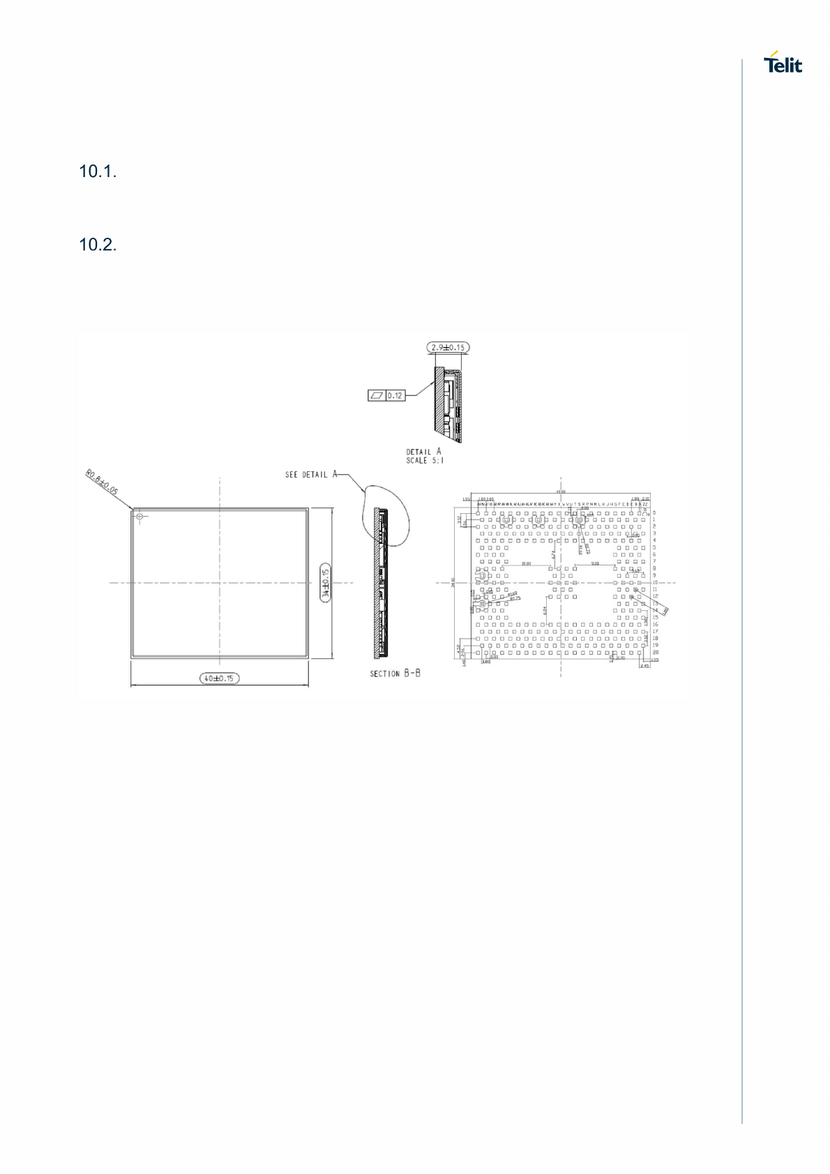
LE920A4 HW User Guide Mounting the Module on Your Board
Doc#: 1VV0301261 General
Rev. 4.3 Page 98 of 123 2017-12-07
10. Mounting the Module on Your Board
General
The module is designed to be compliant with a standard Pb free soldering process.
Finishing & Dimensions
Figure 24 shows the mechanical dimensions of the module.
Figure 24: Mechanical Dimensions
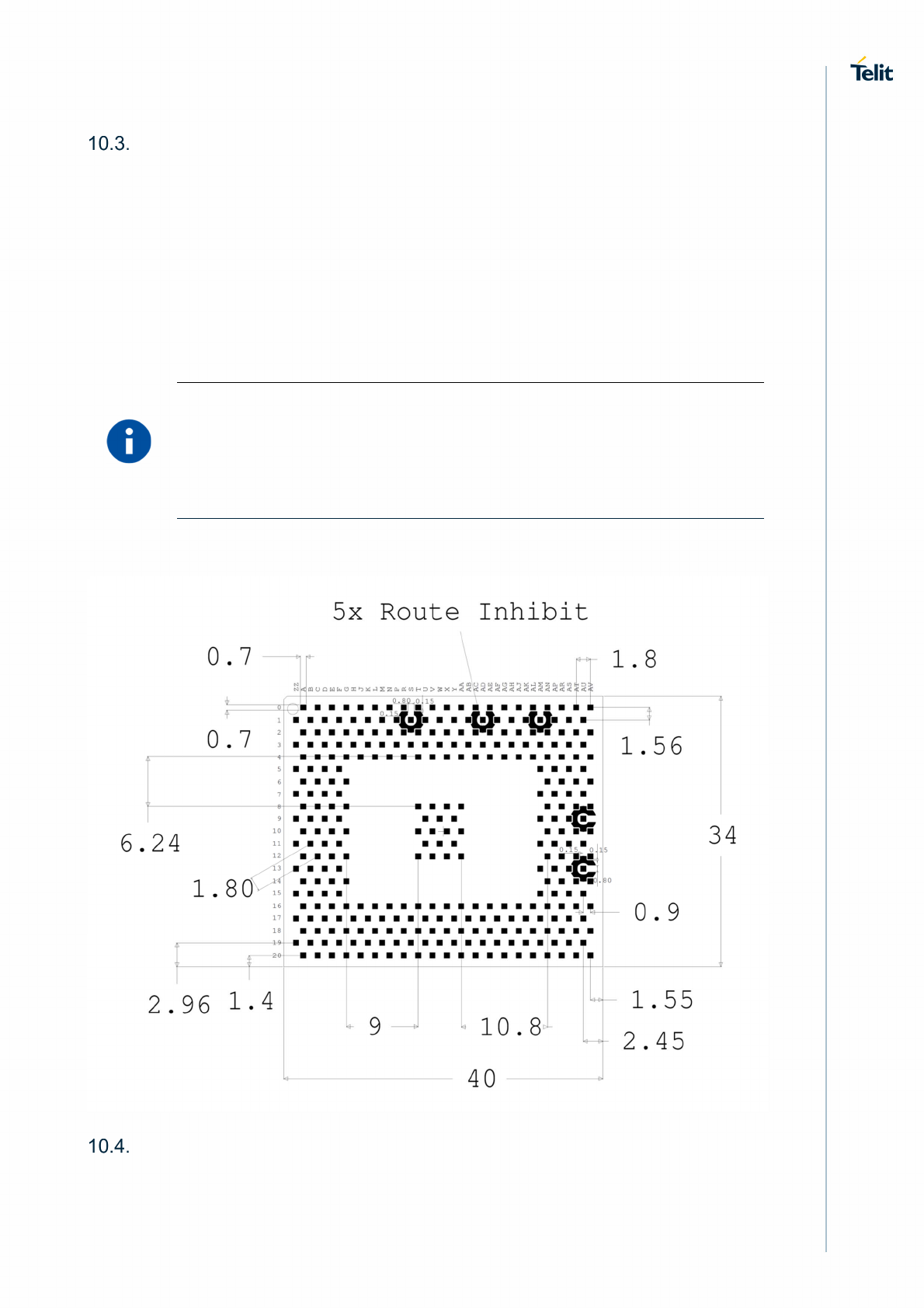
LE920A4 HW User Guide Mounting the Module on Your Board
Doc#: 1VV0301261 Recommended Foot Print for the Application
Rev. 4.3 Page 99 of 123 2017-12-07
Recommended Foot Print for the Application
Figure 25 shows the recommended footprint for the application board (dimensions are in
mm).
To facilitate replacing the module if necessary, it is suggested to design the application
board with a 1.5 mm placement inhibit area around the module.
It is also suggested, as a common rule for an SMT component, to avoid having a
mechanical part of the application board in direct contact with the module.
NOTE:
In the customer application, the 5 crowns marked as INHIBIT in Figure 25
must be clear of signal wiring or ground polygons.
The 5 crown pads should not exist on the customer application board.
Figure 25: Recommended Footprint (Top View)
Stencil
Stencil’s apertures layout can be the same as the recommended footprint (1:1). The
suggested thickness of stencil foil is greater than 120 µm (~5mil).
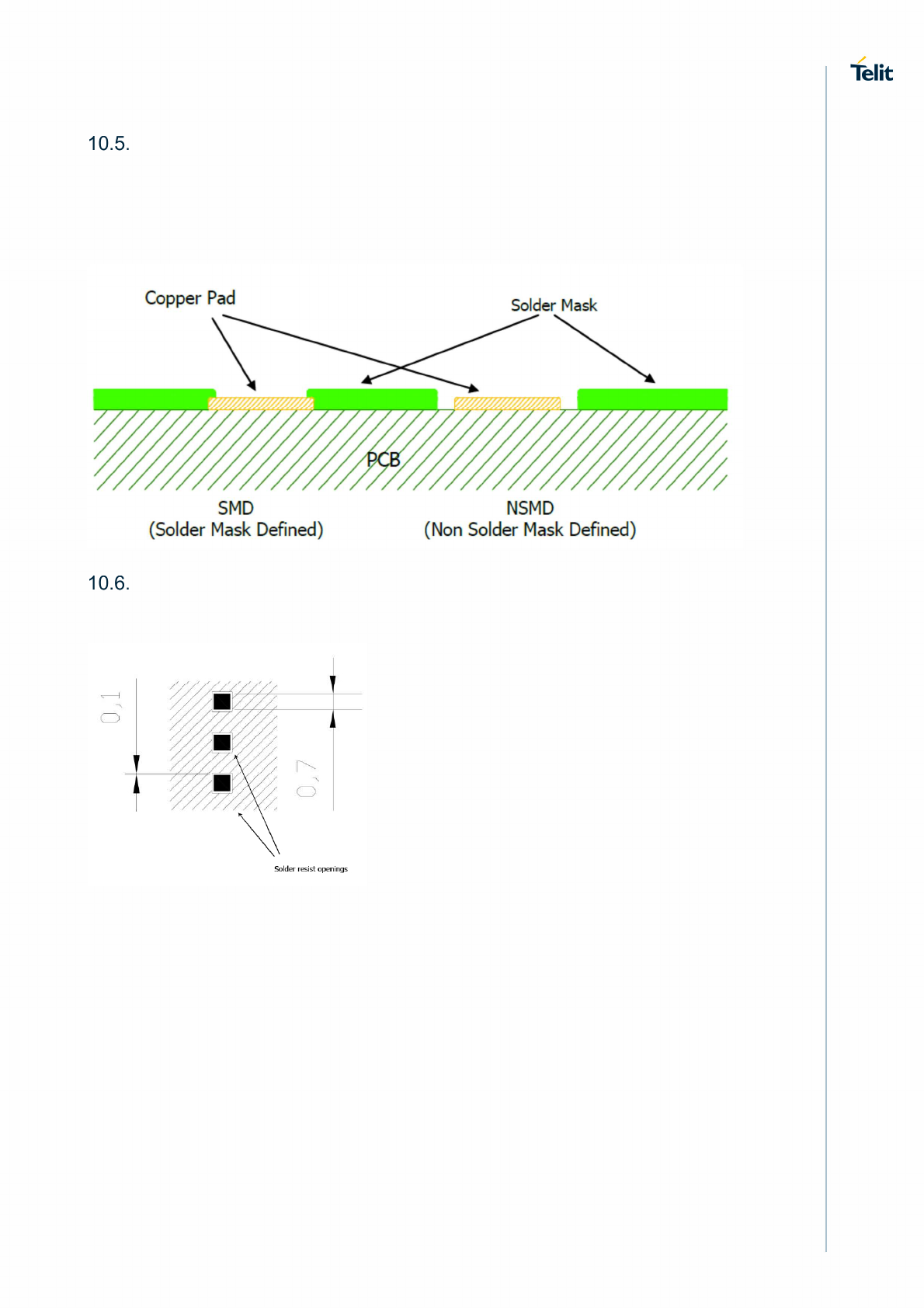
LE920A4 HW User Guide Mounting the Module on Your Board
Doc#: 1VV0301261 PCB Pad Design
Rev. 4.3 Page 100 of 123 2017-12-07
PCB Pad Design
The solder pads on the PCB are recommended to be of the Non Solder Mask Defined
(NSMD) type.
Figure 26: PCB Pad Design
Recommendations for PCB Pad Dimensions (mm)
Figure 27: PCB Pad Dimensions
It is not recommended to place around the pads a via or micro-via that is not covered by
solder resist in an area of 0.15 mm unless it carries the same signal as the pad itself.
Micro via inside the pads are allowed.
Holes in pad are allowed only for blind holes and not for through holes.
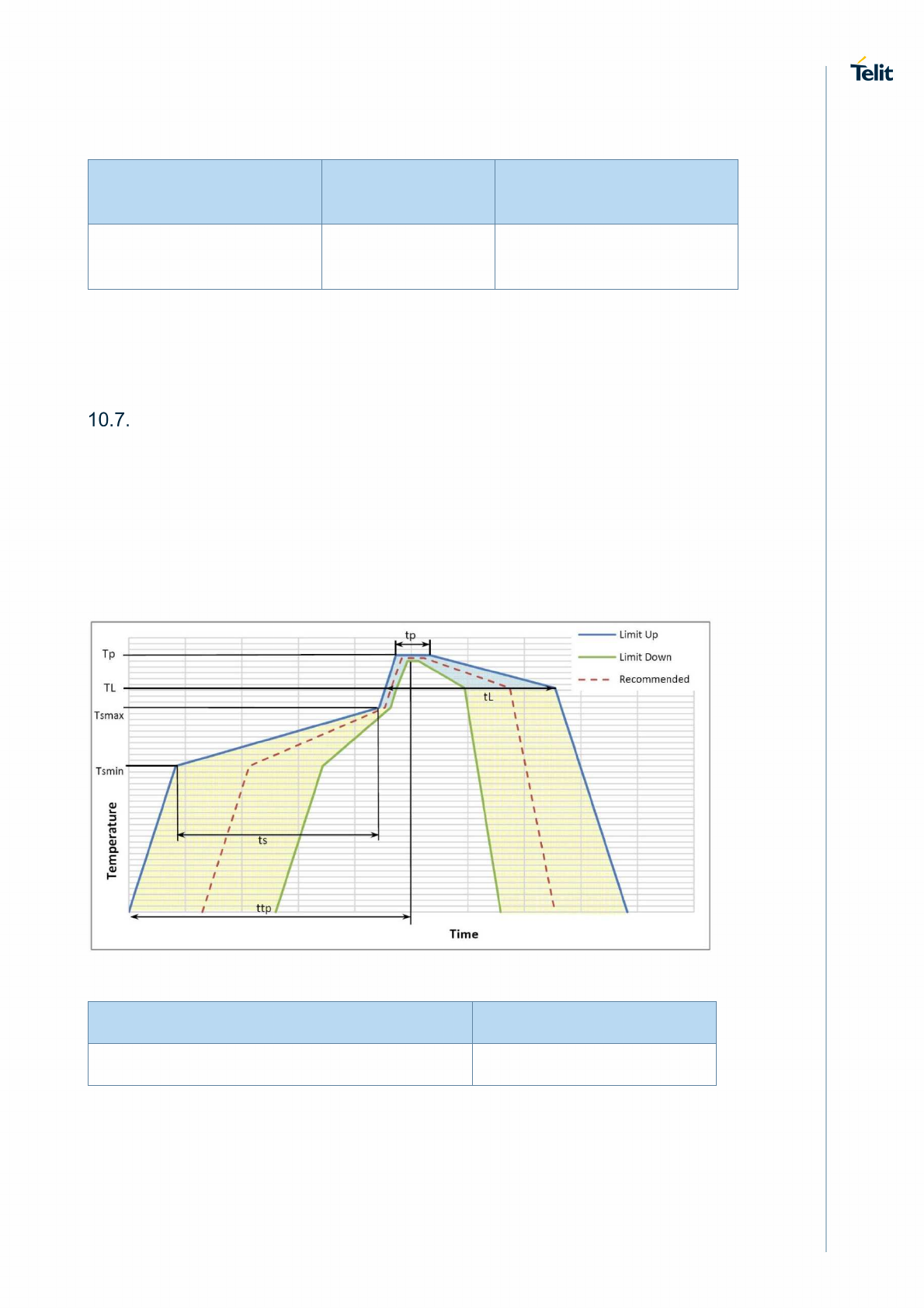
LE920A4 HW User Guide Mounting the Module on Your Board
Doc#: 1VV0301261 Solder Paste
Rev. 4.3 Page 101 of 123 2017-12-07
Table 46: Recommendations for PCB Pad Surfaces
Finish Layer Thickness
(um) Properties
Electro-less Ni / Immersion
Au 3 –7 / 0.05 – 0.15 Good solder ability protection,
high shear force values
The PCB must be able to resist the higher temperatures that occur during the lead-free
process. This issue should be discussed with the PCB supplier. Generally, the wettability
of tin-lead solder paste on the described surface plating is better compared to lead-free
solder paste.
Solder Paste
It is recommended to use only “no clean” solder paste to avoid cleaning of the modules
after assembly.
10.7.1. Solder Reflow
Figure 28 shows the recommended solder reflow profile.
Figure 28: Solder Reflow Profile
Table 47: Solder Profile Characteristics
Profile Feature Pb-Free Assembly
Average ramp-up rate (T
L
to T
P
) 3°C/second max
LE920A4 HW User Guide Mounting the Module on Your Board
Doc#: 1VV0301261 Solder Paste
Rev. 4.3 Page 102 of 123 2017-12-07
Profile Feature Pb-Free Assembly
Preheat
– Temperature Min (Tsmin)
– Temperature Max (Tsmax)
– Time (min to max) (ts)
150°C
200°C
60-180 seconds
Tsmax to TL
– Ramp-up rate
3°C/second max
Time maintained above:
– Temperature (TL)
– Time (tL)
217°C
60-150 seconds
Peak temperature (Tp) 245 +0/-5°C
Time within 5°C of actual peak temperature (tp) 10-30 seconds
Ramp-down rate 6°C/second max.
Time 25°C to peak temperature 8 minutes max.
NOTE:
All temperatures refer to the top side of the package, measured on the
package body surface.
WARNING:
The module withstands one reflow process only.

LE920A4 HW User Guide Application Guide
Doc#: 1VV0301261 Debug of the Module in Production
Rev. 4.3 Page 103 of 123 2017-12-07
11. Application Guide
Debug of the Module in Production
To test and debug the mounting of the module, it is strongly recommended to add several
test pads on the host PCB for the following purposes:
• Checking the connection between the module itself and the application board
• Testing the performance of the module by connecting it with an external computer
Depending on the customer application, these pads include, but are not limited to the
following signals:
• TXD
• RXD
• ON/OFF
• SHDN_N
• RESET_N
• GND
• VBATT
• TX_AUX
• RX_AUX
• USB_VBUS
• USB_D+
• USB_D-
• GPIO20
• WCI_RX
In addition, the following signals are also recommended (but not mandatory):
• PWRMON
• STAT_LED
• SW_RDY

LE920A4 HW User Guide Application Guide
Doc#: 1VV0301261 Bypass Capacitor on Power Supplies
Rev. 4.3 Page 104 of 123 2017-12-07
Bypass Capacitor on Power Supplies
When a sudden voltage step is asserted to the module, or a sudden cut of the power
supply occurs, the steep transition causes an overshoot or undershoot. This abrupt
voltage transition can affect the device, causing it not to operate or to malfunction. Bypass
capacitors are needed to alleviate this behavior. Customers must pay special attention to
this issue while designing the application board.
The length and width of the power lines must be considered carefully, and values of the
bypass capacitors must be selected accordingly.
The capacitors also prevent a ripple of the power supplies and the switching noise caused
in TDMA systems, such as GSM.
In particular, suitable bypass capacitors must be placed on the following lines within the
application board:
• VBATT & VBATT_PA
(Pads AP17,AP19,AR18,AR20,AS17,AS19,AT18,AU17,AU19,AT20)
• USB_VBUS (Pad A18)
Recommended values are:
• 100 uF for both VBATT and VBATT_PA together
• 4.7uF for USB_VBUS (including the 1uF capacitor inside the module)
The capacitance mainly depends on the condition of the application board. In general,
higher capacitance values are required for longer power lines.
LE920A4 HW User Guide Application Guide
Doc#: 1VV0301261 SIM Interface
Rev. 4.3 Page 105 of 123 2017-12-07
SIM Interface
This section presents the recommended schematics for the design of SIM interfaces on
the application boards. The module supports two external SIM interfaces.
11.3.1. SIM Schematic Example
Figure 29 illustrates in particular how to design the application side and which values to
assign the components.
Figure 29: SIM Schematics
NOTE:
The resistor value on SIMIO pulled up to SIMVCC must be defined to be
compliant with the 3GPP specification for USIM electrical testing.
The module contains an internal pull-up resistor of 20K Ω on SIMIO.
However, the un-mounted option in the application design can be
recommended to tune R1 if necessary.
The value of the C1 capacitor to be applied with the module is 100 nF.
EMC Recommendations
All signals in the module are provided with some EMC protection. Nevertheless, the
accepted level differs according to specific pin. Table 48 lists the characteristics.
Table 48: EMC Recommendations
Pad Signal I/O Function Contact
Air
All pins
All pins All pins ± 4KV ± 8KV

LE920A4 HW User Guide Application Guide
Doc#: 1VV0301261 Download and Debug Port
Rev. 4.3 Page 106 of 123 2017-12-07
Pad Signal I/O Function Contact
Air
Antenna
AD1,AU9,S1
Antenna
pads
Analog
I/O
Antenna pad ± 4KV ± 8KV
Appropriate series resistors must be considered to protect the input lines from
overvoltage.
Download and Debug Port
This section provides recommendations for the design of the host system for downloading
or upgrading the Telit software and for debugging the module when it is already mounted
on a host system.
• For downloading or upgrading the Telit software:
Updating the firmware by the host is only possible via USB and not via UART.
If the USB interface is not used, it is highly recommended to place an optional
USB connector on the application board. At the minimum, test points of the USB
signals are required to enable SW update.
• For debugging the module:
USB and Auxiliary UART interfaces are used for debugging the module. If the USB
and AUX UART interfaces are not used, it is highly recommended to place optional
connectors on the application board. At least, test points of the USB and AUX
UART signals are required for debugging purposes.
11.5.1. Fast Boot Mode
Fast Boot mode is normally used by Telit software to enter SW Download mode.
Fast Boot mode is triggered by GPIO_20 (PAD AN4). Asserting this signal high (1.8V)
during boot will force the system into Fast Boot mode.
11.5.2. Recovery Boot Mode
A Recovery Boot Download mode is used if a corrupted boot image was flashed into the
device or if all other recovery modes failed.
Recovery Boot Download mode is triggered by the WCI_RX signal (PAD AT2). Asserting
this signal high (1.8V) during boot will force the system into Recovery Boot Download
mode.

LE920A4 HW User Guide Application Guide
Doc#: 1VV0301261 Antenna Detection
Rev. 4.3 Page 107 of 123 2017-12-07
NOTE:
The application board must support accessible test pads on the GPIO_20
and WCI_RX signals to enable the download recovery modes mentioned
above.
Antenna Detection
The module provides an antenna detection application, indicating for each of the cellular
and GNSS antennas whether it is shorted to ground or open.
Refer to Ref 7: Antenna Detection Application Note.

LE920A4 HW User Guide Packing System
Doc#: 1VV0301261 Tray
Rev. 4.3 Page 108 of 123 2017-12-07
12. Packing System
Tray
The module can be packed on trays.
The tray is JEDEC compliant, injection molded antistatic Modified Polyphenylene ether
(MPPO). It has good thermal characteristics and can withstand a standard baking
temperature of up to 125°C, thereby avoiding handling the modules if baking is required.
The trays are rigid, thus providing mechanical protection against transport stress. In
addition, they are re-usable and so environmentally sustainable.
There are 2 (two) antistatic rubber bands that enclose each envelope.
The carton box is rigid, offering mechanical protection. The carton box has one flap across
the entire top surface. It is sealed with tape along the edges of the box.
Table 49: Tray Packing
Modules per
Tray Trays per
Envelope Modules per
Envelope Envelopes per
Carton Box Modules per
Box
24 5 + 1 empty 120 4 480
Table 50: Packing Quantities
Order Type Quantity
Minimum Order Quantity (MOQ) 24
Standard Packing Quantity (SPQ) 480
LE920A4 HW User Guide Packing System
Doc#: 1VV0301261 Tray
Rev. 4.3 Page 109 of 123 2017-12-07
Each tray contains 24 pieces as shown in Figure 30.
Figure 30: Tray Packing
LE920A4 HW User Guide Packing System
Doc#: 1VV0301261 Tray
Rev. 4.3 Page 110 of 123 2017-12-07
Figure 31: Packing Tray Drawing
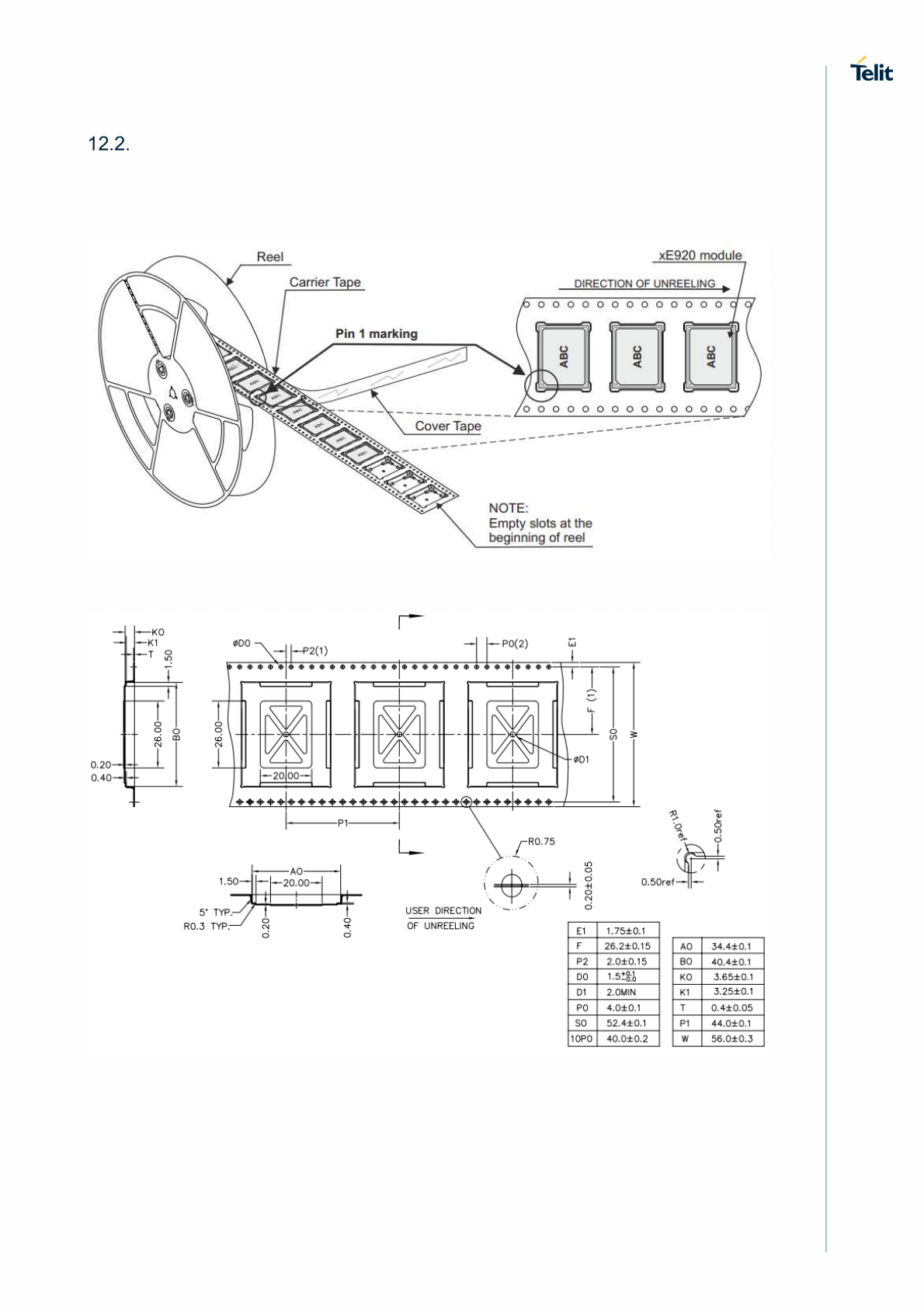
LE920A4 HW User Guide Packing System
Doc#: 1VV0301261 Tape & Reel
Rev. 4.3 Page 111 of 123 2017-12-07
Tape & Reel
The module can be packed on tape & reels of 200 pieces each.
Figure 32: Module Positioning into the Carrier
Figure 33: Carrier Tape Detail
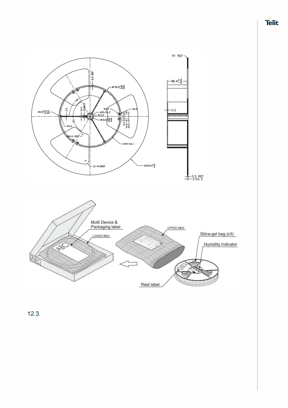
LE920A4 HW User Guide Packing System
Doc#: 1VV0301261 Moisture Sensitivity
Rev. 4.3 Page 112 of 123 2017-12-07
Figure 34: Reel Detail
Figure 35: Reel Box Detail
Moisture Sensitivity
The module is a Moisture Sensitive Device Level 3, in accordance with standard
IPC/JEDEC J-STD-020. Observe all the requirements for using this kind of component.

LE920A4 HW User Guide Safety Recommendations
Doc#: 1VV0301261 Moisture Sensitivity
Rev. 4.3 Page 113 of 123 2017-12-07
13. Safety Recommendations
READ CAREFULLY
Be sure that the use of this product is allowed in your country and in the environment
required. The use of this product may be dangerous and must be avoided in the following
areas:
• Where it can interfere with other electronic devices in environments such as
hospitals, airports, aircrafts, etc.
• Where there is risk of explosion such as gasoline stations, oil refineries, etc.
It is the responsibility of the user to enforce the country regulations and the specific
environment regulations.
Do not disassemble the product; any mark of tampering will compromise the warranty
validity.
It is recommended following the instructions of the hardware user guides for correct wiring
of the product. The product must be supplied with a stabilized voltage source and the
wiring conform to the security and fire prevention regulations.
The product must be handled with care, avoiding any contact with the pins because
electrostatic discharges may damage the product itself. The same caution must be taken
for the SIM, checking carefully the instructions for its use. Do not insert or remove the SIM
when the product is in power saving mode.
The system integrator is responsible for the functioning of the final product; therefore, care
must be taken of the external components of the module, as well as of any project or
installation issue, because of the risk of disturbing the GSM network or external devices or
having any impact on safety. Should there be any doubt, please refer to the technical
documentation and the regulations in force.
Every module must be equipped with a proper antenna with the specified characteristics.
The antenna must be installed with care in order to avoid any interference with other
electronic devices and must be installed with the guarantee of a minimum 20 cm distance
from a human body. In case this requirement cannot be satisfied, the system integrator
must assess the final product against the SAR regulation.
The European Community provides some Directives for electronic equipment introduced
on the market. All the relevant information is available on the European Community
website:
http://europa.eu.int/comm/enterprise/rtte/dir99-5.htm
The text of the Directive 99/05 regarding telecommunication equipment is available, while
the applicable Directives (Low Voltage and EMC) are available at:
http://europa.eu.int/comm/enterprise/rtte/dir99-5.htm
LE920A4 HW User Guide Conformity assessment issues
Doc#: 1VV0301261 FCC/ISED Regulatory notices
Rev. 4.3 Page 114 of 123 2017-12-07
14. Conformity assessment issues
FCC/ISED Regulatory notices
Modification statement
Telit has not approved any changes or modifications to this device by the user. Any changes or
modifications could void the user’s authority to operate the equipment.
Telit n’approuve aucune modification apportée à l’appareil par l’utilisateur, quelle qu’en soit la
nature. Tout changement ou modification peuvent annuler le droit d’utilisation de l’appareil par
l’utilisateur.
Interference statement (if it is not placed in the device)
This device complies with Part 15 of the FCC Rules and Industry Canada licence-exempt RSS
standard(s). Operation is subject to the following two conditions: (1) this device may not cause
interference, and (2) this device must accept any interference, including interference that may
cause undesired operation of the device.
Le présent appareil est conforme aux CNR d'Industrie Canada applicables aux appareils radio
exempts de licence. L'exploitation est autorisée aux deux conditions suivantes : (1) l'appareil ne doit
pas produire de brouillage, et (2) l'utilisateur de l'appareil doit accepter tout brouillage
radioélectrique subi, même si le brouillage est susceptible d'en compromettre le fonctionnement.
Wireless notice
This device complies with FCC/ISED radiation exposure limits set forth for an uncontrolled
environment and meets the FCC radio frequency (RF) Exposure Guidelines and RSS-102 of the ISED
radio frequency (RF) Exposure rules.
Antenna gain must be below:
Band
Freq [MHz]
Gain [dBi]
GSM 850
850
3
.6
4
EGPRS 850
850
3
.6
4
PCS 1900
1900
2.51
EGPRS 1900
1900
2.51
WCDMA
Band 2
1900
8.01
WCDMA Band 4
1700
5.00
WCDMA Band 5
850
5.00
FDD II
1900
8.01
FDD IV
1700
5.00
FDD V
850
5.00
FDD VII
700
8.01
FDD XII
700
5.63
This transmitter must not be co-located or operating in conjunction with any other antenna or
transmitter.
Le présent appareil est conforme à l'exposition aux radiations FCC / ISED définies pour un
environnement non contrôlé et répond aux directives d'exposition de la fréquence de la FCC
LE920A4 HW User Guide Conformity assessment issues
Doc#: 1VV0301261 FCC/ISED Regulatory notices
Rev. 4.3 Page 115 of 123 2017-12-07
radiofréquence (RF) et RSS-102 de la fréquence radio (RF) ISED règles d'exposition. Gain de
l'antenne doit être ci-dessous:
Band Freq [MHz] Gain [dBi]
GSM 850
850
3
.6
4
EGPRS 850
850
3
.6
4
PCS 1900
1900
2.51
EGPRS 1900
1900
2.51
WCDMA Band 2
1900
8.01
WCDMA Band 4
1700
5.00
WCDMA Band 5
850
5.00
FDD II
1900
8.01
FDD IV
1700
5.00
FDD V
850
5.00
FDD VII
700
8.01
FDD XII
700
5.63
L'émetteur ne doit pas être colocalisé ni fonctionner conjointement avec à autre
antenne ou autre émetteur.
FCC Class B digital device notice
This equipment has been tested and found to comply with the limits for a Class B digital device,
pursuant to part 15 of the FCC Rules. These limits are designed to provide reasonable protection
against harmful interference in a residential installation. This equipment generates, uses and can
radiate radio frequency energy and, if not installed and used in accordance with the instructions,
may cause harmful interference to radio communications. However, there is no guarantee that
interference will not occur in a particular installation. If this equipment does cause harmful
interference to radio or television reception, which can be determined by turning the equipment
off and on, the user is encouraged to try to correct the interference by one or more of the following
measures:
- Reorient or relocate the receiving antenna.
- Increase the separation between the equipment and receiver.
- Connect the equipment into an outlet on a circuit different from that to which the receiver
is connected.
- Consult the dealer or an experienced radio/TV technician for help.
LE920A4 NA
Contains FCC ID:
RI7LE920A4NA
Contains IC: 5131A-LE920A4NA
CAN ICES-3 (B) / NMB-3 (B)
This Class B digital apparatus complies with Canadian ICES-003.
Cet appareil numérique de classe B est conforme à la norme canadienne ICES -003.

LE920A4 HW User Guide Acronyms
Doc#: 1VV0301261 FCC/ISED Regulatory notices
Rev. 4.3 Page 116 of 123 2017-12-07
15. Acronyms
ADC Analog-to-Digial Converter
AE Application-enabled
CLK Clock
CMOS Complementary Metal – Oxide Semiconductor
CS Chip Select
DAC Digital-to-Analog Converter
DTE Data Terminal Equipment
ESR Equivalent Series Resistance
FDD Frequency Division Duplex
GLONASS Global Orbiting Navigation Satellite System
GNSS Global Navigation Satellite System
GPIO General Purpose Input/Output
GPRS General Packet Radio Services
GPS Global Positioning System
GSM Global System for Mobile communications
HS High Speed
HSDPA High-Speed Downlink Packet Access
HSIC High-Speed Inter-Chip

LE920A4 HW User Guide Acronyms
Doc#: 1VV0301261 FCC/ISED Regulatory notices
Rev. 4.3 Page 117 of 123 2017-12-07
HSUPA High-Speed Uplink Packet Access
I/O Input/Output
I2C Inter-Integrated Circuit
LTE Long Term Evolution
MISO Master Input – Slave Output
MOSI Master Output – Slave Input
MRDY Master Ready
PCB Printed Circuit Board
RTC Real Time Clock
SD Secure Digital
SGMII Serial Gigabit Media-Independent Interface
SIM Subscriber Identification Module
SOC System-on-Chip
SPI Serial Peripheral Interface
SRDY Slave Ready
TTSC Telit Technical Support Centre
UART Universal Asynchronous Receiver Transmitter
UMTS Universal Mobile Telecommunication System
USB Universal Serial Bus

LE920A4 HW User Guide Acronyms
Doc#: 1VV0301261 FCC/ISED Regulatory notices
Rev. 4.3 Page 118 of 123 2017-12-07
VNA Vector Network Analyzer
VSWR Voltage Standing Wave Radio
WCDMA Wideband Code Division Multiple Access
WCI Wireless Coexistence Interface

LE920A4 HW User Guide Document History
Doc#: 1VV0301261 FCC/ISED Regulatory notices
Rev. 4.3 Page 119 of 123 2017-12-07
16. Document History
Table 51: Document History
Revisi
on Date Changes
4.3 2017-12-07 Section 6.2.2 – Adding notes that GPRS Class 12 is for LE920A4-
EU and LE920A4-CN variants. GPRS Class10 is for LE920A4-NA
variant.
4.2 2017-11-23 Section 2.7 – Renamed from Sensitivity to RF parameters and
added TX output power section (2.7.2)
Section 3.1 - Removed duplication of description related to
USB_VBUS.
Section 3.1 – Correct typo related to ETH_INT_N pin.
Section 5.2 – Added clarification regarding ON_OFF.
Section 7.5 – Added note related to GPS port and GPS LNA.
Section 8.1 – Added clarification regarding VBUS supply.
Section 8.1.1 – Added description for OTG connectivity.
Section 8.3 - Added reference to Ethernet card application note.
Section 8.3 – Added clarification regarding ETH_INT_N pin.
Section 8.6.2 – Updated analog Microphone parameter.
Section 14.1 – Updated GSM 850MHz and EGPRS 850MHz Max
antenna gain.
4.1 2017-08-08 Section 2.8 – Added note about the module label thickness
Section 8.4.1 – Clarified a note related to DTR
4 2017-07-12 Document formatting by a New Template
Section 2.6.1, Table 5 - Modified RF bands of the AP variant
Section 11.5 – Modified text
Section 12.1 – The Minimum Order Quantity is 24 units
3.5 2017-04-05 Updated reference documents table
Section 8.4 - Added note regarding DTR
Section 8.6 – Added Analog Audio Characteristics
Section 11.4 – Updated ESD values
3.4 2017-04-05 Section 2.6.2 – Changed B41 to B41M
Adding Section 14: FCC/ISED Regulatory notices

LE920A4 HW User Guide Document History
Doc#: 1VV0301261 FCC/ISED Regulatory notices
Rev. 4.3 Page 120 of 123 2017-12-07
Revisi
on Date Changes
3.3 2017-01-03 Remove “Preliminary” label
Section 1.5: Updated “Related Documents” table
Section 2.3: Added more info on memory supported options
Section 3.1: Added PHY control interface
Section 3.3: Updated LGA “PinMap” Drawing
Section 5.3.3: Added clarification about RESET_N usage
Section 5.3.4: Added Figure for SHDN_N power down timing
Section 8.1: Added info related to USB OTG
Section 8.3: Added info related to PHY control interface
Section 8.5.3: Added clarification about VMMC
Section 8.6.2: Added clarification about I2S support
Section 9.2: Added clarification about RTC
Section 9.7: Added GNSS characteristics
Section 10.2: Updated mechanical drawing
Section 10.3: Updated application footprint drawing
3.2 2016-12-16 Updated Applicability table
3.1 2016-11-27 Section 4.3.2 : Added note regarding pull resistance of special
GPIO’s.
Section 8.7.2 : Added info regarding wakeup from GPIO’s.
Section 10.3 : Updated application board footprint drawing
Section 1.5 : Updated link to WIFI application note

LE920A4 HW User Guide Document History
Doc#: 1VV0301261 FCC/ISED Regulatory notices
Rev. 4.3 Page 121 of 123 2017-12-07
Revisi
on Date Changes
3.0 2016-09-01 Official Release;
Merged and updated the Applicability table (p.2) based on
previous Section 1.6
Section 1.5 : Updated the table of related documents
Section 2.6.1 : Updated the table of RF bands
Section 3.1 : Few updates in the table of pin-out
Section 6.1 : Added voltage ripple requirement
Section 6.1: Table 18 : Added current consumption values
Section 9.1: Updated description
Section 9.2: Updated the RTC consumption
Section 9.4.1: Updated description
Section 11.5: Added sub-sections 11.5.1 and 11.5.2
Section 12: Updated table
Section 12.2 : Added information about Tape & Reel packing
General editing and formatting
2.7 2016-06-15 Official Release;
Sec. 2.5.1: Storage temp. is 105 deg.C max.
Sec. 3.1 : Updates about pads E8, AN8
Previous Sec. 4.2 (Limiting Values) – Removed
New Sec. 4.2 : Updated min. supply voltage levels
Sec 4.3 : Updated Logic Level Specification
Sec 5.3.3: Updated Reset connection (added future support)
Sec 5.2: Updated “Initialization and Activation state”
Sec. 5.3.3 : Added recommendation and diagram for future
compatibility
Sec. 8 : All hardware interfaces are gathered under this section
A summary table of the module interfaces is presented
Updated number of available GPIO’s inside the summary
table
Sec. 8.6.2 : Updated the Digital Audio specifications
Sec. 9.4.1 : Updated the ADC range of input level
Sec. 10.3 : Updated the “Recommended footprint” figure
(was previously mistaken)
Added “PRELIMINARY” on top of each page

LE920A4 HW User Guide Document History
Doc#: 1VV0301261 FCC/ISED Regulatory notices
Rev. 4.3 Page 122 of 123 2017-12-07
Revisi
on Date Changes
2.2 2016-04-12 Official Release;
Moved RoHS paragraph from 2.8.3 to 2.5.1
Sections 4.3 & 6.1: VBAT min is 3.4V (not 3.3V)
Added Sec. 15.5 (now 9.5): Temperature Monitor Function
2.0 2016-03-23 Official Release;
General update – Added Datasheet related sections
Added Sec. 1.6: Product Variants
Added Sec. 2.2: Applications
Added Sec. 2.3: General Functionality
Added Sec. 2.4: Block Diagram
Modified Sec. 2.6: Frequency Bands
Added Sec. 3: Functional Description
Changed ESD values to TBD (until tested)
Added Sec. 5: Backward compatibility to LE920
Modified Sec. 7.5 : GNSS Antenna Requirements
Added Sec. 15.6 (now 9.6): Fuel Gauge
Added Sec. 17.6 (now 11.6): Antenna Detection
1.0 2016-02-14 Official Release;
Section 2.5.1: Channels corrected for WCDMA B4.
Section 2.5.1: LTE B17 replaced by LTE B12
Section 2.5.2: Added table for LE920A4 -EU
Section 2.6: Sensitivity typical values updated
Section 7.1: Main antenna requirements updated
Section 7.4: Diversity antenna requirements updated
0.5 2015-12-20 First Draft