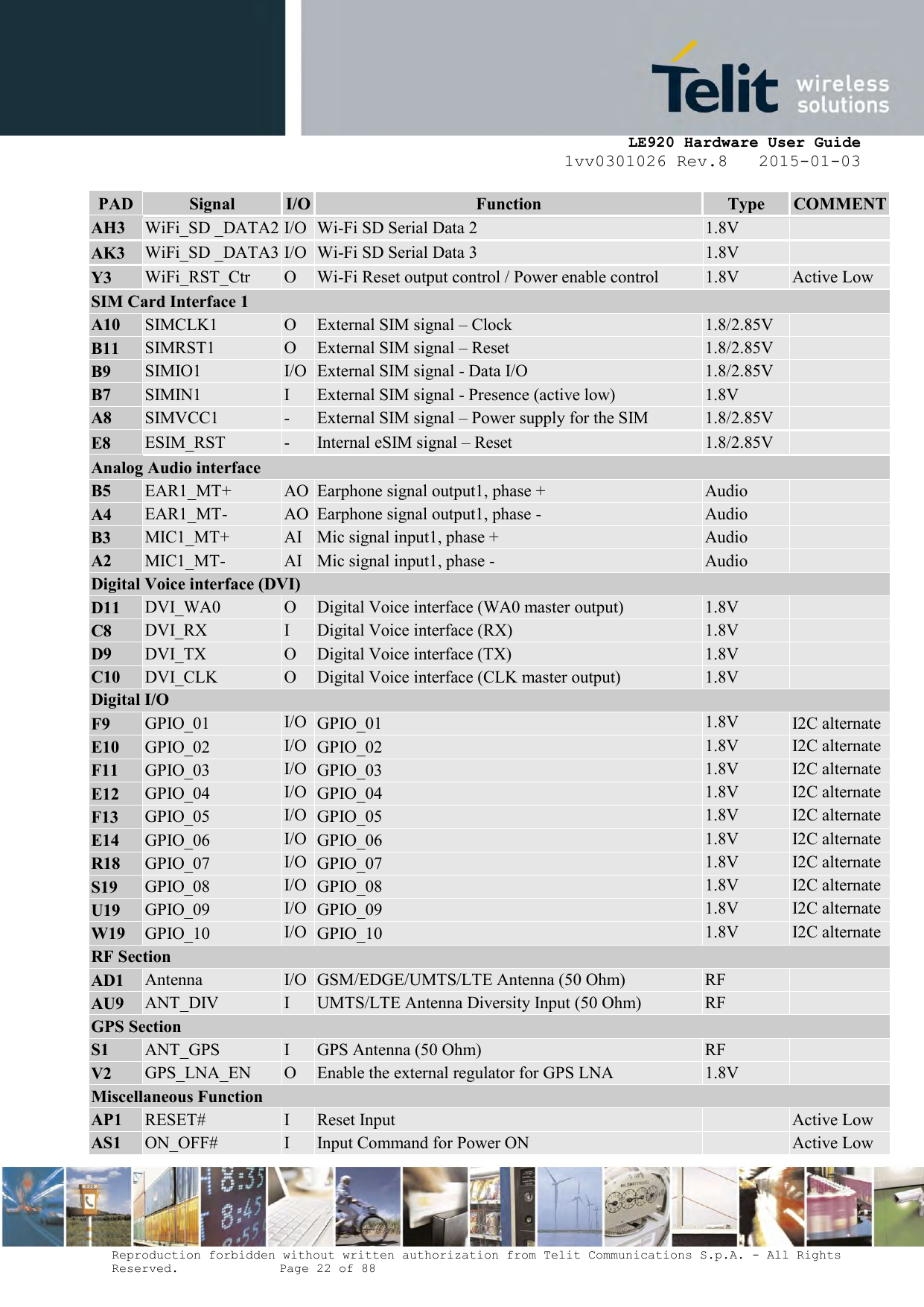
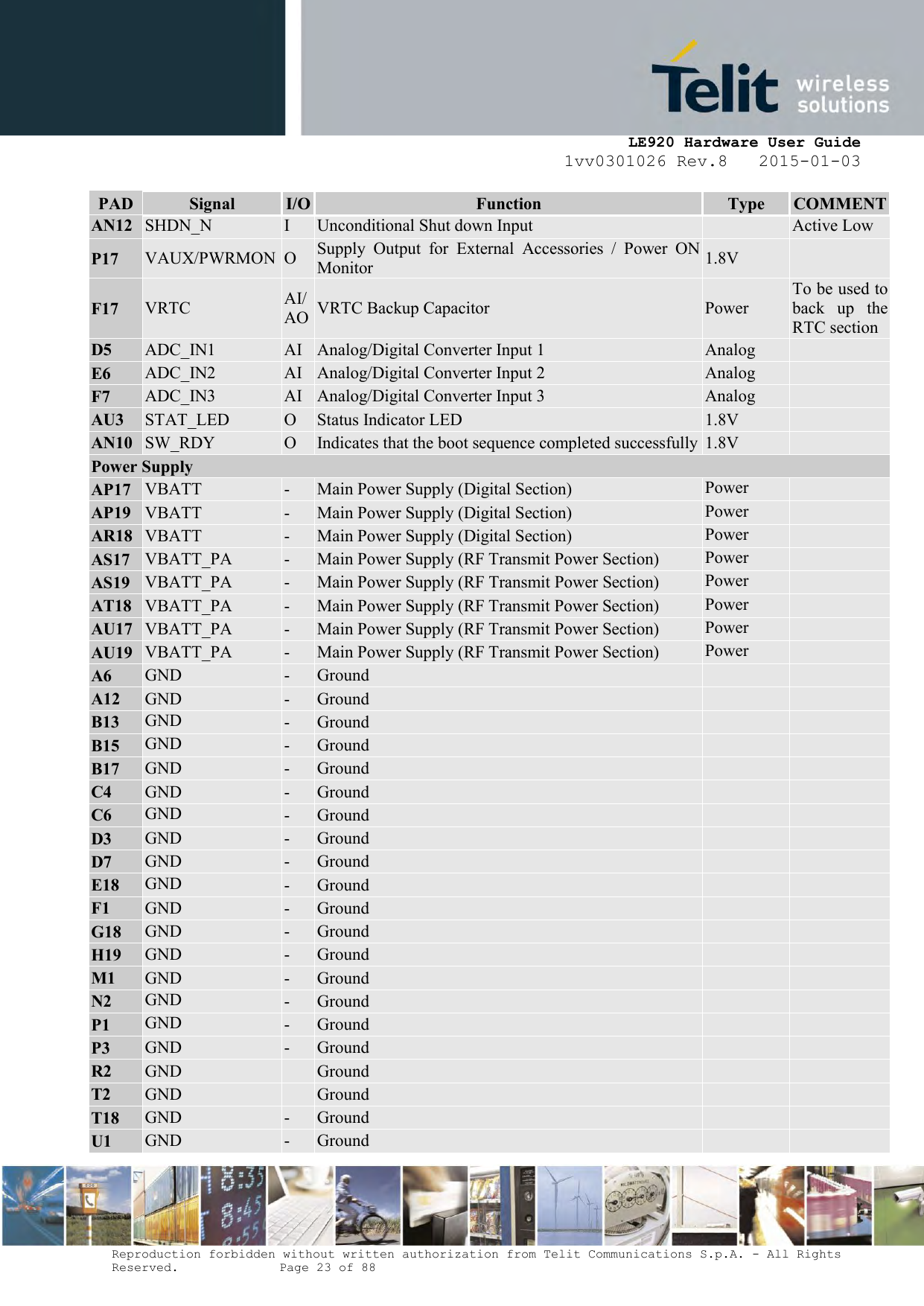
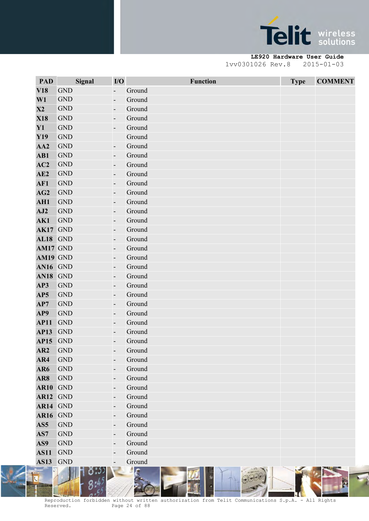
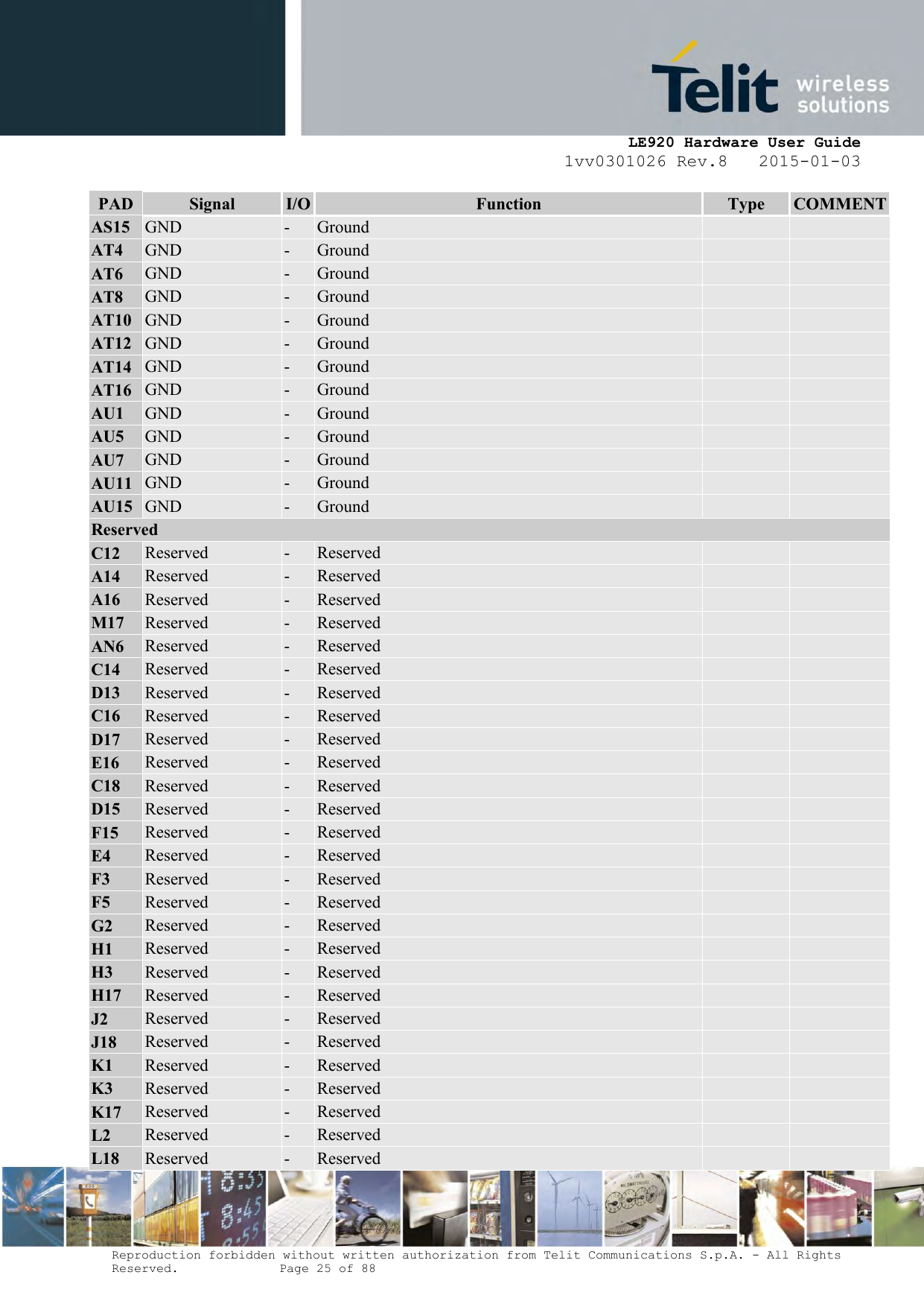
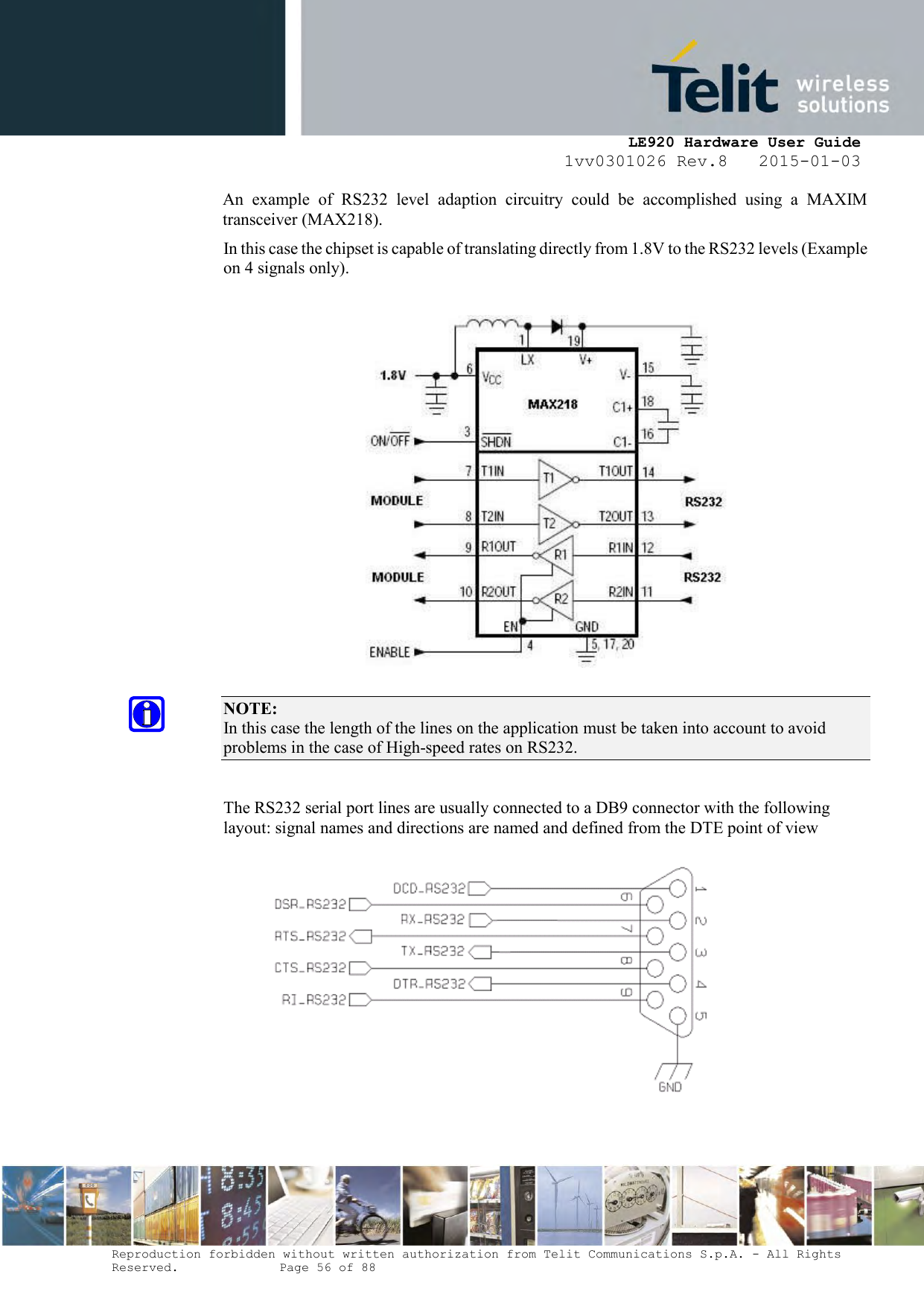
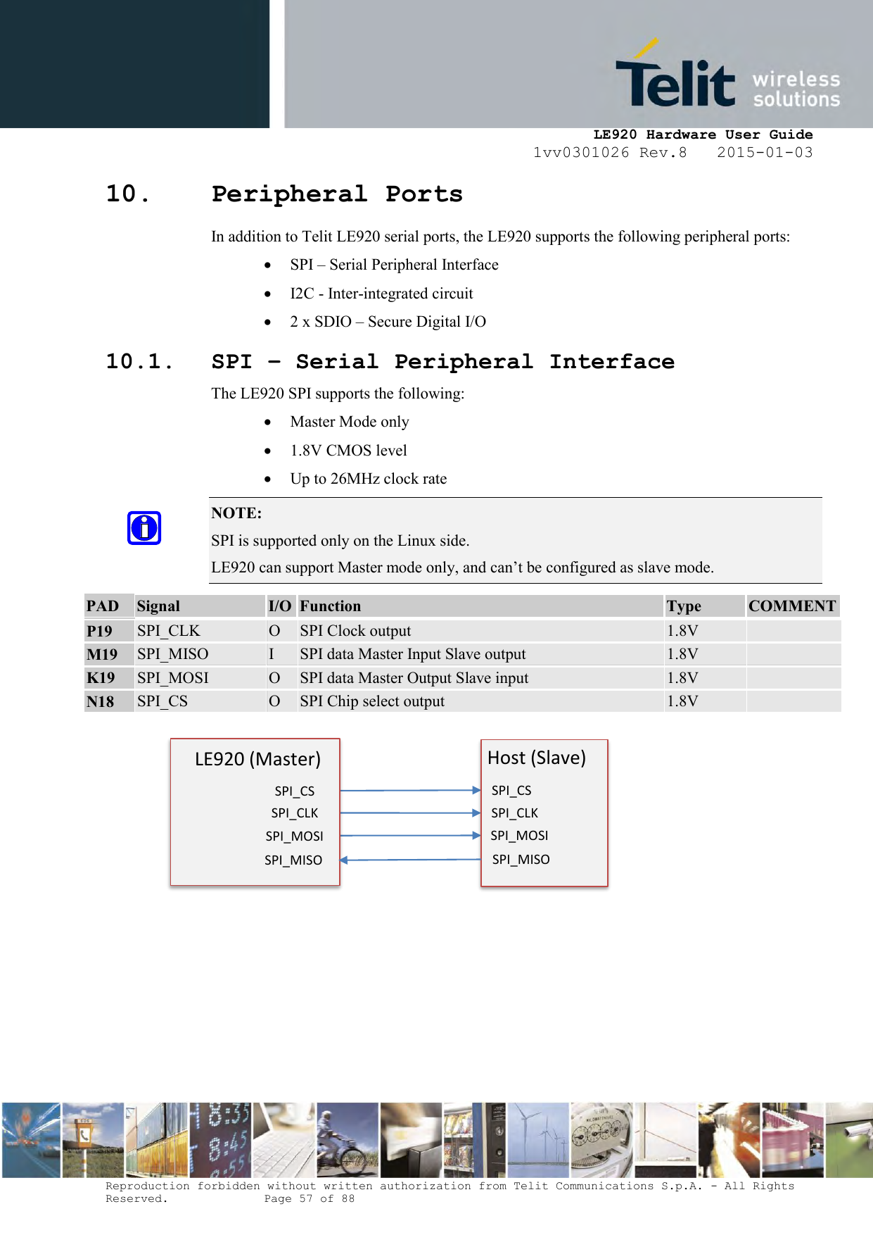
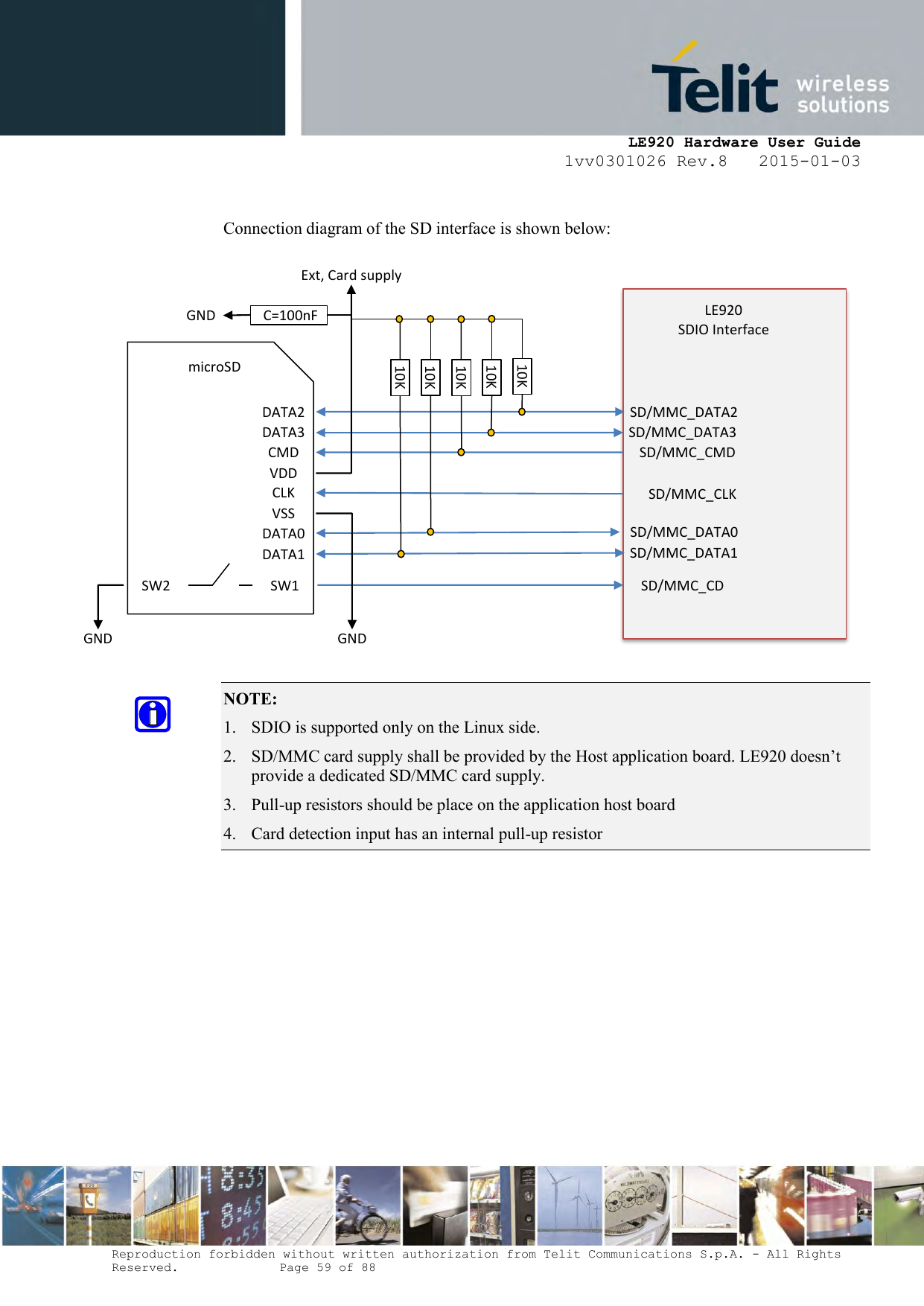
Telit Communications S p A LE920NA1 LE920-NA LTE Module User Manual HW User Guide

Telit Communications S.p.A. LE920-NA LTE Module HW User Guide

User Manual

                    LE920 Hardware User Guide  1vv0301026 Rev.9 - 2016-03-29
    LE920 Hardware User Guide 1vv0301026 Rev.8   2015-01-03 Reproduction forbidden without written authorization from Telit Communications S.p.A. - All Rights Reserved.    Page 2 of 88  APPLICABILITY TABLE  PRODUCT  LE920-EUG (cs1550f-B) LE920-NAG (cs1550f-A) LE920-EU (cs1647c) LE920-NA (cs1701) LE920-CN (cs1648D) LE920-NA AUTO S (cs1717)    APPLICABILITY TABLE 1
    LE920 Hardware User Guide 1vv0301026 Rev.8   2015-01-03 Reproduction forbidden without written authorization from Telit Communications S.p.A. - All Rights Reserved.    Page 3 of 88  SPECIFICATIONS SUBJECT TO CHANGE WITHOUT NOTICE Notice While reasonable efforts have been made to assure the accuracy of this document, Telit assumes no liability resulting from any inaccuracies or omissions in this document, or from use of the information obtained herein. The information in this document has been carefully checked and is believed to be entirely reliable. However, no responsibility is assumed for inaccuracies or omissions.  Telit  reserves  the  right  to  make  changes  to  any  products  described  herein  and reserves the right to revise this document and to make changes from time to time in content hereof with no obligation to notify any person of revisions or changes. Telit does not assume any liability arising out of the application or use of any product, software, or circuit described herein; neither does it convey license under its patent rights or the rights of others. It is possible that this publication may contain references to, or information about Telit products (machines and programs), programming, or services that are not announced in your country. Such references or information must not be construed to mean that Telit intends to announce such Telit products, programming, or services in your country. Copyrights This instruction manual and the Telit products described in this instruction manual may be, include  or  describe  copyrighted  Telit  material,  such  as  computer  programs  stored  in semiconductor memories or other media. Laws in the Italy and other countries preserve for Telit and its licensors certain exclusive rights for copyrighted material, including the exclusive right to  copy,  reproduce  in  any  form,  distribute  and  make  derivative  works  of  the  copyrighted material. Accordingly, any copyrighted material of Telit and its licensors contained herein or in  the  Telit  products  described  in  this  instruction  manual  may  not  be  copied,  reproduced, distributed, merged or modified in any manner without the express written permission of Telit. Furthermore, the purchase of Telit products shall not be deemed to grant either directly or by implication,  estoppel,  or  otherwise,  any  license  under  the  copyrights,  patents  or  patent applications of Telit, as arises by operation of law in the sale of a product. Computer Software Copyrights The Telit and 3rd Party supplied Software (SW) products described in this instruction manual may  include  copyrighted  Telit  and  other  3rd  Party  supplied  computer  programs  stored  in semiconductor memories or other media. Laws in the Italy and other countries preserve for Telit and other 3rd Party supplied SW certain exclusive rights for copyrighted computer programs, including  the  exclusive  right  to  copy  or  reproduce  in  any  form  the  copyrighted  computer program.  Accordingly,  any  copyrighted  Telit  or  other  3rd  Party  supplied  SW  computer programs contained in the Telit products described in this instruction manual may not be copied (reverse engineered) or reproduced in any manner without the express written permission of Telit or the 3rd Party SW supplier. Furthermore, the purchase of Telit products shall not be deemed to grant either directly or by implication, estoppel, or otherwise, any license under the copyrights, patents or patent applications of Telit or other 3rd Party supplied SW, except for the normal non-exclusive, royalty free license to use that arises by operation of law in the sale of a product.
    LE920 Hardware User Guide 1vv0301026 Rev.8   2015-01-03 Reproduction forbidden without written authorization from Telit Communications S.p.A. - All Rights Reserved.    Page 4 of 88  Usage and Disclosure Restrictions License Agreements The software described in this document is the property of Telit and its licensors. It is furnished by express license agreement only and may be used only in accordance with the terms of such an agreement. Copyrighted Materials Software  and  documentation  are  copyrighted  materials.  Making  unauthorized  copies  is prohibited by law. No part of the software or documentation may be reproduced, transmitted, transcribed, stored in a retrieval system, or translated into any language or computer language, in any form or by any means, without prior written permission of Telit High Risk Materials Components, units, or third-party products used in the product described herein are NOT fault-tolerant and are NOT designed, manufactured, or intended for use as on-line control equipment in the following hazardous environments requiring fail-safe controls: the operation of Nuclear Facilities, Aircraft Navigation or Aircraft Communication Systems, Air Traffic Control, Life Support, or Weapons Systems (“High Risk Activities"). Telit and its supplier(s) specifically disclaim any expressed or implied warranty of fitness for such High Risk Activities. Trademarks TELIT and the Stylized T Logo are registered in Trademark Office. All other product or service names are the property of their respective owners.   Copyright © Telit Communications S.p.A. 2015.
    LE920 Hardware User Guide 1vv0301026 Rev.8   2015-01-03 Reproduction forbidden without written authorization from Telit Communications S.p.A. - All Rights Reserved.    Page 5 of 88  Contents 1. Introduction ................................................. 9 1.1. Scope ..................................................... 9 1.2. Audience .................................................. 9 1.3. Contact Information, Support .............................. 9 1.4. Document Organization .................................... 10 1.5. Text Conventions ......................................... 11 1.6. Related Documents ........................................ 11 2. General Product Description ................................. 12 2.1. Overview ................................................. 12 2.2. LE920 Mechanical Dimensions .............................. 13 2.3. Weight ................................................... 13 2.4. Environmental requirements ............................... 14 2.4.1. Temperature range .......................................... 14 2.4.2. RoHS compliance ............................................ 14 2.5. Operating Frequency ...................................... 15 2.5.1. LE920-EUG(cs1550f-B), LE920-EU (cs1647c) ................... 15 2.5.2. LE920-NAG (cs1550f-A) ...................................... 15 2.5.3. LE920-NA (cs1701), LE920-NA AUTO S (cs1717) ................ 16 2.5.4. LE920-CN (cs1648D) ......................................... 17 2.6. Sensitivity .............................................. 18 2.7. Conformity assessment issues .............................. 18 2.7.1. FCC/IC Regulatory notices .................................. 18 2.7.1.1. Modification statement .................................. 18 2.7.1.2. Interference statement .................................. 18 2.7.1.3. RF exposure ............................................. 18 2.7.1.4. FCC Class B digital device notice ....................... 19 2.7.1.5. Labelling Requirements for the Host device .............. 19 3. LE920 Module Connections .................................... 21 3.1. PIN-OUT .................................................. 21 3.1.1. LGA Pads Layout ............................................ 28 4. Hardware Commands ........................................... 29 4.1. Turning ON the LE920 ..................................... 29
    LE920 Hardware User Guide 1vv0301026 Rev.8   2015-01-03 Reproduction forbidden without written authorization from Telit Communications S.p.A. - All Rights Reserved.    Page 6 of 88  4.2. Initialization and Activation state ...................... 29 4.3. Turning OFF the LE920 .................................... 30 4.3.1. Shutdown by Software Command ............................... 31 4.3.2. Hardware Shutdown .......................................... 32 4.3.3. Hardware Unconditional Restart (RESET) ..................... 33 4.3.4. Hardware Unconditional Shutdown ............................ 34 4.4. Summary of Turning ON and OFF the module ................. 35 5. Power Supply ................................................ 36 5.1. Power Supply Requirements ................................ 36 5.2. General Design Rules ..................................... 38 5.2.1. Electrical Design Guidelines ............................... 38 5.2.1.1. + 5V Input Source Power Supply Design Guidelines ........ 38 5.2.1.2. + 12V Input Source Power Supply Design Guidelines ....... 39 5.2.1.3. Battery Source Power Supply Design Guidelines ........... 41 5.2.2. Thermal Design Guidelines .................................. 42 5.2.3. Power Supply PCB Layout Guidelines ......................... 43 6. Antenna(s) .................................................. 45 6.1. GSM/WCDMA/LTE Antenna Requirements ....................... 45 6.2. GSM/WCDMA/LTE Antenna – PCB line Guidelines .............. 46 6.3. GSM/WCDMA/LTE Antenna – Installation Guidelines .......... 47 6.4. Antenna Diversity Requirements ........................... 47 6.5. GPS/GNSS Antenna Requirements ............................ 48 6.5.1. Combined GPS/GNSS Antenna .................................. 49 6.5.2. Linear and Patch GPS/GNSS Antenna .......................... 49 6.5.3. Front End Design Considerations ............................ 49 6.5.4. GPS/GNSS Antenna - PCB Line Guidelines ..................... 50 6.5.5. GPS/GNSS Antenna – Installation Guidelines ................. 50 7. Logic Level Specifications .................................. 51 8. USB Port .................................................... 52 9. Serial Ports ................................................ 53 9.1. Modem Serial Port 1 ...................................... 54 9.2. Modem Serial Port 2 ...................................... 55 9.3. RS232 Level Translation .................................. 55
    LE920 Hardware User Guide 1vv0301026 Rev.8   2015-01-03 Reproduction forbidden without written authorization from Telit Communications S.p.A. - All Rights Reserved.    Page 7 of 88  10. Peripheral Ports ............................................ 57 10.1. SPI – Serial Peripheral Interface ...................... 57 10.2. I2C - Inter-integrated circuit ......................... 58 10.3. SDIO – Secure Digital I/O .............................. 58 10.4. Wi-Fi (SDIO) control Interface ......................... 60 11. Audio Section Overview ...................................... 61 11.1. Analog Audio ........................................... 61 11.2. Digital Audio .......................................... 61 12. General Purpose I/O ......................................... 63 12.1. Logic Level Specifications ............................. 64 12.2. Using a GPIO Pad as Input .............................. 64 12.3. Using a GPIO Pad as Output ............................. 65 12.4. Using the Temperature Monitor Function ................. 65 12.4.1. Short Description ........................................ 65 12.5. Indication of Network Service Availability ............. 66 12.6. RTC Bypass ............................................. 67 12.7. VAUX Power Output ...................................... 67 13. ADC section ................................................. 68 13.1. ADC Converter .......................................... 68 13.1.1. Description .............................................. 68 13.1.2. Using ADC Converter ...................................... 68 14. Mounting the module on your board ........................... 69 14.1. General ................................................ 69 14.2. Finishing & Dimensions ................................. 69 14.3. Recommended foot print for the application ............. 70 14.4. Stencil ................................................ 71 14.5. PCB Pad Design ......................................... 71 14.6. Recommendations for PCB Pad Dimensions (mm) ............ 72 14.7. Solder Paste ........................................... 73 14.7.1. Solder Reflow ............................................ 73 15. Application guide ........................................... 75
    LE920 Hardware User Guide 1vv0301026 Rev.8   2015-01-03 Reproduction forbidden without written authorization from Telit Communications S.p.A. - All Rights Reserved.    Page 8 of 88  15.1. Debug of the LE920 in production ....................... 75 15.2. Bypass capacitor on Power supplies ..................... 76 15.3. SIM interface .......................................... 77 15.3.1. SIM schematic example .................................... 77 15.3.2. eSIM interface guidelines ................................ 78 15.4. EMC recommendations .................................... 80 15.5. Download and Debug Port ................................ 81 16. Packing system .............................................. 82 16.1. Tray Drawing ........................................... 84 16.2. Moisture Sensitivity ................................... 85 17. Safety Recommendations ...................................... 86 18. Document History ............................................ 87 - Adding section 2.7 Conformity assessment issues ............................. 88
    LE920 Hardware User Guide 1vv0301026 Rev.8   2015-01-03 Reproduction forbidden without written authorization from Telit Communications S.p.A. - All Rights Reserved.    Page 9 of 88  1. Introduction 1.1. Scope The aim of this document is to present possible and recommended hardware solutions useful for developing a product with the Telit LE920 module. All the features and solutions detailed are applicable to all LE920, where “LE920” refers to the modules listed in the applicability table. If a specific feature is applicable to a specific product, it will be clearly highlighted.  NOTICE: The description text “LE920” refers to all modules listed in the APPLICABILITY TABLE 1.  1.2. Audience This document is intended for Telit customers, especially system integrators, about to implement their applications using our LE920 module. 1.3. Contact Information, Support For general contact, technical support, to report documentation errors and to order manuals, contact Telit’s Technical Support Center (TTSC) at: TS-EMEA@telit.com TS-NORTHAMERICA@telit.com TS-LATINAMERICA@telit.com TS-APAC@telit.com Alternatively, use:  http://www.telit.com/en/products/technical-support-center/contact.php For detailed information about where you can buy the Telit modules or for recommendations on accessories and components visit:  http://www.telit.com To  register  for  product  news  and  announcements  or  for  product  questions  contact  Telit’s Technical Support Center (TTSC). Our aim is to make this guide as helpful as possible. Keep us informed of your comments and suggestions for improvements. Telit appreciates feedback from the users of our information.
    LE920 Hardware User Guide 1vv0301026 Rev.8   2015-01-03 Reproduction forbidden without written authorization from Telit Communications S.p.A. - All Rights Reserved.    Page 10 of 88  1.4. Document Organization  This document contains the following chapters:  Chapter 1: “Introduction” provides a scope for this document, target audience, contact and support information, and text conventions.  Chapter 2: “General Product Description”  gives an overview of the features of the product.  Chapter 3: “LE920 Module Connections” deals with the pin out configuration and layout.  Chapter 4: “Hardware Commands” instructs how to control the module via hardware  Chapter 5: “Power Supply” deals with supply and consumption.  Chapter 6: “Antenna” The antenna connection and board layout design are the most important parts in the full product design  Chapter 7: “Logic Level specifications” Specific values adopted in the implementation of logic levels for this module.            Chapter 8: “USB Port”    Chapter 9: “Serial Ports”    Chapter 10: “Peripheral Ports”    Chapter 11: “Audio Section Overview”    Chapter 12: “General Purpose I/O” How the general purpose I/O pads can be configured.  Chapter 13 “DAC and ADC Section” Deals with these two kind of analog converters.  Chapter 14: “Mounting the module on your board”    Chapter 15: “Application Guides”    Chapter 16: “Packing System”    Chapter 17: “Safety Recommendations”    Chapter 18: “Document History”
    LE920 Hardware User Guide 1vv0301026 Rev.8   2015-01-03 Reproduction forbidden without written authorization from Telit Communications S.p.A. - All Rights Reserved.    Page 11 of 88  1.5. Text Conventions  Danger – This information MUST be followed or catastrophic equipment failure or bodily injury may occur.  Caution or Warning – Alerts the user to important points about integrating the module, if these points are not followed, the module and end user equipment may fail or malfunction.  Tip or Information – Provides advice and suggestions that may be useful when integrating the module.  All dates are in ISO 8601 format, i.e. YYYY-MM-DD. 1.6. Related Documents   LE920-EUG/NAG Product Description, 80407ST10118A  LE920-EUG/NAG AT command reference guide, 80407ST10116A  Telit EVK2 User Guide, 1vv0300704  Telit xE920 Audio Settings Application Note, 80404NT10095A
    LE920 Hardware User Guide 1vv0301026 Rev.8   2015-01-03 Reproduction forbidden without written authorization from Telit Communications S.p.A. - All Rights Reserved.    Page 12 of 88  2. General Product Description 2.1. Overview  The aim of this document is to present possible and recommended hardware solutions useful for developing a product with the Telit LE920 module. In this document all the basic functions of a wireless module will be taken into account; for each one of them a valid hardware solution will be suggested and usually incorrect solutions and common errors to be avoided will be highlighted. Obviously this document cannot embrace every hardware solution or every product that may be designed. Obviously avoiding invalid solutions must be considered as mandatory. Whereas the suggested hardware configurations need not be considered mandatory, the information given should be used as a guide and a starting point for properly developing your product with the Telit LE920 module. . NOTICE: The integration of the GSM/GPRS/EGPRS/WCDMA/HSPA+/LTE LE920 cellular module within user application must be done according to the design rules described in this manual.     The information presented in this document is believed to be accurate and reliable. However, no responsibility is assumed by Telit Communication S.p.A. for its use, such as any infringement of patents or other rights of third parties which may result from its use. No license is granted by implication or otherwise under any patent rights of Telit Communication S.p.A. other than for circuitry embodied in Telit products. This document is subject to change without notice.
    LE920 Hardware User Guide 1vv0301026 Rev.8   2015-01-03 Reproduction forbidden without written authorization from Telit Communications S.p.A. - All Rights Reserved.    Page 13 of 88  2.2. LE920 Mechanical Dimensions The Telit LE920 module overall dimensions are:  •  Length:   34 mm , +/- 0.15 mm Tolerance •  Width:    40 mm , +/- 0.15 mm Tolerance •  Thickness:   2.9 mm , +/- 0.13 mm Tolerance  2.3. Weight  The module weight of LE920 is about 9.0 gram.
    LE920 Hardware User Guide 1vv0301026 Rev.8   2015-01-03 Reproduction forbidden without written authorization from Telit Communications S.p.A. - All Rights Reserved.    Page 14 of 88  2.4. Environmental requirements 2.4.1. Temperature range    Operating Temperature Range –40°C ~ +85°C Storage and non-operating Temperature Range –40°C ~ +85°C  2.4.2. RoHS compliance As a part of Telit corporate policy of environmental protection, the LE920 complies with the RoHS (Restriction of Hazardous Substances) directive of the European Union (EU directive 2011/65/EU).
    LE920 Hardware User Guide 1vv0301026 Rev.8   2015-01-03 Reproduction forbidden without written authorization from Telit Communications S.p.A. - All Rights Reserved.    Page 15 of 88  2.5. Operating Frequency The operating frequencies in GSM850, EGSM900, DCS1800, PCS1900, WCDMA & LTE modes are conformed to the 3GPP specifications.  2.5.1. LE920-EUG(cs1550f-B), LE920-EU (cs1647c)  Mode Freq. TX (MHz) Freq. RX (MHz) Channels TX - RX offset GSM850 824 ~ 849  869 ~ 894 128 ~ 251 45 MHz EGSM900 890 ~ 915 935 ~ 960 0 ~ 124 45 MHz 880 ~ 890 925 ~ 935 975 ~ 1023 45 MHz DCS1800 1710 ~ 1785 1805 ~ 1880 512 ~ 885 95MHz PCS1900 1850 ~ 1910 1930 ~ 1990 512 ~ 810 80MHz WCDMA2100 – B1 1920 ~ 1980 2110 ~ 2170 Tx: 9612 ~ 9888 Rx: 10562 ~ 10838 190MHz WCDMA1800 – B3 1710 ~ 1785 1805 ~ 1880 Tx: 937 ~ 1288 Rx: 1162 ~ 1513 95MHz WCDMA900 – B8 880 ~ 915 925 ~ 960 Tx: 2712 ~ 2863 Rx: 2937 ~ 3088 45MHz LTE2100 – B1 1920 ~ 1980 2110 ~ 2170 Tx: 18000 ~ 18599 Rx: 0 ~ 599  190MHz LTE1800 – B3 1710 ~ 1785 1805 ~ 1880 Tx: 19200 ~ 19949 Rx: 1200 ~ 1949 95MHz LTE2600 – B7 2500 ~ 2570 2620 ~ 2690 Tx: 20750 ~ 21449 Rx: 2750 ~ 3449 120MHz LTE900 – B8 880 ~ 915 925 ~ 960 Tx: 21450 ~ 21799 Rx: 3450 ~ 3799 45MHz LTE800 – B20 832 ~ 862 791 ~ 821 Tx: 24150 ~ 24449 Rx: 6150 ~ 6449 -41MHz 2.5.2. LE920-NAG (cs1550f-A) Mode Freq. TX (MHz) Freq. RX (MHz) Channels TX - RX offset GSM850 824 ~ 849  869 ~ 894 128 ~ 251 45 MHz EGSM900 890 ~ 915 935 ~ 960 0 ~ 124 45 MHz 880 ~ 890 925 ~ 935 975 ~ 1023 45 MHz DCS1800 1710 ~ 1785 1805 ~ 1880 512 ~ 885 95MHz PCS1900 1850 ~ 1910 1930 ~ 1990 512 ~ 810 80MHz WCDMA2100 – B1 1920 ~ 1980 2110 ~ 2170 Tx: 9612 ~ 9888 Rx: 10562 ~ 10838 190MHz
LE920 Hardware User Guide 1vv0301026 Rev.8   2015-01-03 Reproduction forbidden without written authorization from Telit Communications S.p.A. - All Rights Reserved.    Page 16 of 88 WCDMA1900 – B2 1850 ~ 1910 1930 ~ 1990 Tx: 9262 ~ 9538 Rx: 9662 ~ 9938 80MHz WCDMA1700 – B4 1710 ~ 1755 2110 ~ 2155 Tx: 1312 ~ 1513 Rx: 1537 ~ 1738 400 MHz WCDMA850 – B5 824 ~ 849 869 ~ 894 Tx: 4132 ~ 4233 Rx: 4357 ~ 4458 45MHz WCDMA800 – B6 830 ~ 840 875 ~ 885 Tx: 4162 ~ 4188 Rx: 4387 ~ 4413 45MHz LTE2100 – B1 1920 ~ 1980 2110 ~ 2170 Tx: 18000 ~ 18599 Rx: 0 ~ 599  190MHz LTE1900 – B2 1850 ~ 1910 1930 ~ 1990 Tx: 18600 ~ 19199 Rx: 600 ~ 1199 80MHz LTE1700 – B4 1710~ 1755 2110 ~ 2155 Tx: 19950 ~ 20399 Rx: 1950 ~ 2399 400MHz LTE850 – B5 824 ~ 849 869 ~ 894 Tx: 20400 ~ 20649 Rx: 2400 ~ 2649 45MHz LTE700 – B17 704 ~ 716 734 ~ 746 Tx: 23730 ~ 23849 Rx: 5730 ~ 5849 30MHz 2.5.3. LE920-NA (cs1701), LE920-NA AUTO S (cs1717) Mode  Freq. TX (MHz)  Freq. RX (MHz)  Channels  TX - RX offset WCDMA1900 – B2 1850 ~ 1910 1930 ~ 1990 Tx: 9262 ~ 9538 Rx: 9662 ~ 9938 80MHz WCDMA1700 – B4 1710 ~ 1755 2110 ~ 2155 Tx: 1312 ~ 1513 Rx: 1537 ~ 1738 400 MHz WCDMA850 – B5 824 ~ 849 869 ~ 894 Tx: 4132 ~ 4233 Rx: 4357 ~ 4458 45MHz LTE1900 – B2 1850 ~ 1910 1930 ~ 1990 Tx: 18600 ~ 19199 Rx: 600 ~ 1199 80MHz
LE920 Hardware User Guide 1vv0301026 Rev.8   2015-01-03 Reproduction forbidden without written authorization from Telit Communications S.p.A. - All Rights Reserved.    Page 17 of 88 LTE1700 – B4 1710~ 1755 2110 ~ 2155 Tx: 19950 ~ 20399 Rx: 1950 ~ 2399 400MHz LTE850 – B5 824 ~ 849 869 ~ 894 Tx: 20400 ~ 20649 Rx: 2400 ~ 2649 45MHz LTE2600 – B7 2500 ~ 2570 2620 ~ 2690 Tx: 20750 ~ 21449 Rx: 2750 ~ 3449 120MHz LTE700 – B17 704 ~ 716  734 ~ 746  Tx: 23730 ~ 23849 Rx: 5730 ~ 5849 30MHz 2.5.4. LE920-CN (cs1648D) Mode Freq. TX (MHz) Freq. RX (MHz) Channels TX - RX offset EGSM900 890 ~ 915 935 ~ 960 0 ~ 124 45 MHz 880 ~ 890 925 ~ 935 975 ~ 1023 45 MHz DCS1800 1710 ~ 1785 1805 ~ 1880 512 ~ 885 95MHz WCDMA2100 – B1 1920 ~ 1980 2110 ~ 2170 Tx: 9612 ~ 9888 Rx: 10562 ~ 10838 190MHz WCDMA1800 – B3 1710 ~ 1785 1805 ~ 1880 Tx: 937 ~ 1288 Rx: 1162 ~ 1513 95MHz WCDMA900 – B8 880 ~ 915 925 ~ 960 Tx: 2712 ~ 2863 Rx: 2937 ~ 3088 45MHz LTE2100 – B1 1920 ~ 1980 2110 ~ 2170 Tx: 18000 ~ 18599 Rx: 0 ~ 599  190MHz LTE1800 – B3 1710 ~ 1785 1805 ~ 1880 Tx: 19200 ~ 19949 Rx: 1200 ~ 1949 95MHz LTE900 – B8 880 ~ 915 925 ~ 960 Tx: 21450 ~ 21799 Rx: 3450 ~ 3799 45MHz LTE TDD 2600 – B38 2570 ~ 2620 2570 ~ 2620 Tx: 37750 ~ 38250 Rx: 37750 ~ 38250 0MHz LTE TDD 1900 – B39 1880 ~ 1920 1880 ~ 1920 Tx: 38250 ~ 38650 Rx: 38250 ~ 38650 0MHz LTE TDD 2300 – B40 2300 ~ 2400 2300 ~ 2400 Tx: 38650 ~ 39650 Rx: 38650 ~ 39650 0MHz LTE TDD 2500 – B41 2496 ~ 2690 2496 ~ 2690 Tx: 39650 ~ 41590 Rx: 39650 ~ 41590 0MHz TDSCDMA2000 – B34 2010 ~ 2025 2010 ~ 2025 Tx: 10054 ~ 10121 Rx: 10054 ~ 10121 0MHz TDSCDMA1900 – B39 1880 ~ 1920 1880 ~ 1920 Tx: 9404 ~ 9596 Rx: 9404 ~ 9596 0MHz
    LE920 Hardware User Guide 1vv0301026 Rev.8   2015-01-03 Reproduction forbidden without written authorization from Telit Communications S.p.A. - All Rights Reserved.    Page 18 of 88  2.6. Sensitivity LE920 maximum sensitivity levels are as follow:   -113 dBm @ 2G  -112 dBm @ 3G  -111 dBm @ TD-SCDMA (BW=1.6MHz)  -102 dBm @ 4G FDD (BW=5MHz)  -101 dBm @ 4G TDD (BW=5MHz) 2.7.  Conformity assessment issues 2.7.1. FCC/IC Regulatory notices  2.7.1.1. Modification statement  Telit has not approved any changes or modifications to this device by the user. Any changes or modifications could void the user’s authority to operate the equipment.  Telit n’approuve aucune modification apportée à l’appareil par l’utilisateur, quelle qu’en soit la nature. Tout changement ou modification peuvent annuler le droit d’utilisation de l’appareil par l’utilisateur.  2.7.1.2. Interference statement  This device complies with Part 15 of the FCC  Rules and  Industry Canada licence-exempt RSS standard(s). Operation is subject to the following two conditions: (1) this device may not cause interference, and (2) this device must accept any interference, including interference that may cause undesired operation of the device.  Le présent appareil est  conforme  aux CNR d'Industrie  Canada applicables aux  appareils  radio  exempts de licence.  L'exploitation  est  autorisée  aux  deux  conditions  suivantes  :  (1)  l'appareil  ne  doit  pas  produire  de brouillage,  et  (2)  l'utilisateur  de  l'appareil  doit  accepter  tout  brouillage  radioélectrique  subi,  même  si  le brouillage est susceptible d'en compromettre le fonctionnement.  2.7.1.3. RF exposure  This  equipment  complies  with  FCC  and  IC  radiation  exposure limits  set  forth  for  an  uncontrolled environment. The antenna should be installed and operated with minimum distance of 20 cm between the radiator and your body. Antenna gain must be below:  Frequency band Antenna gain 700 MHz 5,66 dBi 850 MHz 6,13 dBi
    LE920 Hardware User Guide 1vv0301026 Rev.8   2015-01-03 Reproduction forbidden without written authorization from Telit Communications S.p.A. - All Rights Reserved.    Page 19 of 88  1700 MHz 5,00 dBi 1900 MHz 8,01 dBi 2600 MHz 8,01 dBi  This  transmitter  must  not  be  co-located  or  operating  in  conjunction  with  any  other  antenna  or transmitter.  Cet  appareil  est  conforme aux  limites d'exposition aux  rayonnements  de  la  IC  pour  un  environnement non contrôlé. L'antenne doit être installé de façon à garder une distance minimale de 20 centimètres entre la source de rayonnements et votre corps. Gain de l'antenne doit être ci-dessous:  Bande de fréquence Gain de l'antenne 700 MHz 5,66 dBi 850 MHz 6,13 dBi 1700 MHz 5,00 dBi 1900 MHz 8,01 dBi 2600 MHz 8,01 dBi  L'émetteur ne doit pas être colocalisé ni fonctionner conjointement avec à autre antenne ou autre émetteur.    2.7.1.4. FCC Class B digital device notice  This  equipment  has  been  tested  and  found  to  comply  with  the  limits  for  a  Class  B  digital  device, pursuant  to  part  15  of  the  FCC  Rules.  These  limits  are  designed  to  provide  reasonable  protection against harmful interference in a residential installation. This equipment generates, uses and can radiate radio frequency energy and, if not installed and used in accordance with the instructions, may cause harmful interference to radio communications. However, there is no guarantee that interference will not occur in  a particular installation.  If this  equipment  does cause  harmful  interference  to radio  or television  reception,  which  can  be  determined  by  turning  the  equipment  off  and  on,  the  user  is encouraged to try to correct the interference by one or more of the following measures:  - Reorient or relocate the receiving antenna. - Increase the separation between the equipment and receiver.  - Connect the equipment into an outlet on a circuit different from that to which the receiver is connected.  - Consult the dealer or an experienced radio/TV technician for help.  2.7.1.5. Labelling Requirements for the Host device  The host device shall be properly labelled to identify the modules within the host device. The certification label of the module shall be clearly visible at all times when installed in the host device, otherwise the host device must be labelled to display the FCC ID and IC of the module, preceded by the words "Contains transmitter module", or the word "Contains", or similar wording expressing the same meaning, as follows:
    LE920 Hardware User Guide 1vv0301026 Rev.8   2015-01-03 Reproduction forbidden without written authorization from Telit Communications S.p.A. - All Rights Reserved.    Page 20 of 88   Contains FCC ID: RI7LE920NA1 Contains IC: 5131A-LE920NA1  L'appareil hôte doit être étiqueté comme il faut pour permettre l'identification des modules qui s'y trouvent. L'étiquette de certification du module donné doit être posée sur l'appareil hôte à un endroit bien en vue en tout temps. En l'absence d'étiquette, l'appareil hôte doit porter une étiquette donnant le FCC ID et le IC du module, précédé  des  mots  «  Contient  un  module  d'émission  »,  du  mot  «  Contient  »  ou  d'une  formulation  similaire exprimant le même sens, comme suit:  Contains FCC ID: RI7LE920NA1 Contains IC: 5131A-LE920NA1  CAN ICES-3 (B) / NMB-3 (B)  This Class B digital apparatus complies with Canadian ICES-003.  Cet appareil numérique de classe B est conforme à la norme canadienne ICES-003.
    LE920 Hardware User Guide 1vv0301026 Rev.8   2015-01-03 Reproduction forbidden without written authorization from Telit Communications S.p.A. - All Rights Reserved.    Page 21 of 88  3. LE920 Module Connections 3.1. PIN-OUT  PAD Signal I/O Function Type COMMENT USB HS 2.0 Communication Port D19 USB_D+ I/O USB differential Data(+)   F19 USB_D- I/O USB differential Data(-)   A18 USB_VBUS AI Power sense for the internal USB transceiver Power 2.2V – 5.25V @ max 5mA Asynchronous UART – Prog. / data +HW Flow Control AH19 C103/TXD I Serial data input (TXD) from DTE 1.8V  AF19 C104/RXD O Serial data output to DTE 1.8V  AC18 C108/DTR I Input for Data terminal ready signal (DTR) from DTE 1.8V  AA18 C105/RTS I Input for Request to send signal (RTS) from DTE 1.8V  AK19 C106/CTS O Output for Clear to send signal (CTS) to DTE 1.8V  AE18 C109/DCD O Output for Data carrier detect signal (DCD) to DTE 1.8V  AG18 C107/DSR O Output for Data set ready signal (DSR) to DTE 1.8V  AJ18 C125/RING O Output for Ring indicator signal (RI) to DTE 1.8V  Asynchronous Auxiliary UART AB19 TXD_AUX O Auxiliary UART (TX Data to DTE) 1.8V  AD19 RXD_AUX I Auxiliary UART (RX Data from DTE) 1.8V  SPI – Serial Peripheral Interface P19 SPI_CLK O SPI Clock output 1.8V   M19 SPI_MISO I SPI data Master Input Slave output 1.8V   K19 SPI_MOSI O SPI data Master Output Slave input 1.8V   N18 SPI_CS O SPI Chip select output 1.8V   SDIO – Secure Digital I/O AH17 SD/MMC_CMD O SD Command 1.8/2.95V   AD17 SD/MMC_CLK O SD Card Clock 1.8/2.95V   Y17 SD/MMC_DATA0 I/O SD Serial Data 0 1.8/2.95V   AF17 SD/MMC_DATA1 I/O SD Serial Data 1 1.8/2.95V   AB17 SD/MMC_DATA2 I/O SD Serial Data 2 1.8/2.95V   W17 SD/MMC_DATA3 I/O SD Serial Data 3 1.8/2.95V   U17 SD/MMC_CD I SD card detect input 1.8V Active Low  Wi-Fi (SDIO) control Interface AB3 WiFi_SD_CMD O Wi-Fi SD Command 1.8V   AM3 WiFi_SD_CLK O Wi-Fi SD Clock 1.8V   AD3 WiFi_SD _DATA0 I/O Wi-Fi SD Serial Data 0 1.8V   AF3 WiFi_SD _DATA1 I/O Wi-Fi SD Serial Data 1 1.8V
    LE920 Hardware User Guide 1vv0301026 Rev.8   2015-01-03 Reproduction forbidden without written authorization from Telit Communications S.p.A. - All Rights Reserved.    Page 22 of 88  PAD Signal I/O Function Type COMMENT AH3 WiFi_SD _DATA2 I/O Wi-Fi SD Serial Data 2 1.8V   AK3 WiFi_SD _DATA3 I/O Wi-Fi SD Serial Data 3 1.8V   Y3 WiFi_RST_Ctr O Wi-Fi Reset output control / Power enable control 1.8V Active Low  SIM Card Interface 1 A10 SIMCLK1 O External SIM signal – Clock 1.8/2.85V  B11 SIMRST1 O External SIM signal – Reset 1.8/2.85V  B9 SIMIO1 I/O External SIM signal - Data I/O 1.8/2.85V  B7 SIMIN1 I External SIM signal - Presence (active low) 1.8V  A8 SIMVCC1 - External SIM signal – Power supply for the SIM 1.8/2.85V  E8 ESIM_RST - Internal eSIM signal – Reset 1.8/2.85V  Analog Audio interface B5 EAR1_MT+ AO Earphone signal output1, phase + Audio  A4 EAR1_MT- AO Earphone signal output1, phase - Audio  B3 MIC1_MT+ AI Mic signal input1, phase + Audio  A2 MIC1_MT- AI Mic signal input1, phase - Audio  Digital Voice interface (DVI) D11 DVI_WA0 O Digital Voice interface (WA0 master output) 1.8V  C8 DVI_RX I Digital Voice interface (RX) 1.8V  D9 DVI_TX O Digital Voice interface (TX) 1.8V  C10 DVI_CLK O Digital Voice interface (CLK master output) 1.8V  Digital I/O F9 GPIO_01 I/O GPIO_01 1.8V I2C alternate E10 GPIO_02 I/O GPIO_02 1.8V I2C alternate F11 GPIO_03 I/O GPIO_03 1.8V I2C alternate E12 GPIO_04 I/O GPIO_04 1.8V I2C alternate F13 GPIO_05 I/O GPIO_05 1.8V I2C alternate E14 GPIO_06 I/O GPIO_06 1.8V I2C alternate R18 GPIO_07 I/O GPIO_07 1.8V I2C alternate S19 GPIO_08 I/O GPIO_08 1.8V I2C alternate U19 GPIO_09 I/O GPIO_09 1.8V I2C alternate W19 GPIO_10 I/O GPIO_10 1.8V I2C alternate RF Section AD1 Antenna I/O GSM/EDGE/UMTS/LTE Antenna (50 Ohm) RF  AU9 ANT_DIV I UMTS/LTE Antenna Diversity Input (50 Ohm) RF  GPS Section S1 ANT_GPS I GPS Antenna (50 Ohm) RF  V2 GPS_LNA_EN O Enable the external regulator for GPS LNA 1.8V  Miscellaneous Function AP1 RESET# I Reset Input  Active Low AS1 ON_OFF#  I Input Command for Power ON  Active Low
    LE920 Hardware User Guide 1vv0301026 Rev.8   2015-01-03 Reproduction forbidden without written authorization from Telit Communications S.p.A. - All Rights Reserved.    Page 23 of 88  PAD Signal I/O Function Type COMMENT AN12 SHDN_N I Unconditional Shut down Input  Active Low P17 VAUX/PWRMON O Supply  Output  for  External  Accessories  /  Power  ON Monitor 1.8V  F17 VRTC AI/ AO VRTC Backup Capacitor Power To be used to back  up  the RTC section D5 ADC_IN1 AI Analog/Digital Converter Input 1 Analog  E6 ADC_IN2 AI Analog/Digital Converter Input 2 Analog  F7 ADC_IN3 AI Analog/Digital Converter Input 3 Analog  AU3 STAT_LED O Status Indicator LED 1.8V  AN10 SW_RDY O Indicates that the boot sequence completed successfully 1.8V  Power Supply AP17 VBATT - Main Power Supply (Digital Section) Power  AP19 VBATT - Main Power Supply (Digital Section) Power  AR18 VBATT - Main Power Supply (Digital Section) Power  AS17 VBATT_PA - Main Power Supply (RF Transmit Power Section) Power  AS19 VBATT_PA - Main Power Supply (RF Transmit Power Section) Power  AT18 VBATT_PA - Main Power Supply (RF Transmit Power Section) Power  AU17 VBATT_PA - Main Power Supply (RF Transmit Power Section) Power  AU19 VBATT_PA - Main Power Supply (RF Transmit Power Section) Power  A6 GND - Ground   A12 GND - Ground   B13 GND - Ground   B15 GND - Ground   B17 GND - Ground   C4 GND - Ground   C6 GND - Ground   D3 GND - Ground   D7 GND - Ground   E18 GND - Ground   F1 GND - Ground   G18 GND - Ground   H19 GND - Ground   M1 GND - Ground   N2 GND - Ground   P1 GND - Ground   P3 GND - Ground   R2 GND  Ground   T2 GND  Ground   T18 GND - Ground   U1 GND - Ground
    LE920 Hardware User Guide 1vv0301026 Rev.8   2015-01-03 Reproduction forbidden without written authorization from Telit Communications S.p.A. - All Rights Reserved.    Page 24 of 88  PAD Signal I/O Function Type COMMENT V18 GND - Ground   W1 GND - Ground   X2 GND - Ground   X18 GND - Ground   Y1 GND - Ground   Y19 GND  Ground   AA2 GND - Ground   AB1 GND - Ground   AC2 GND - Ground   AE2 GND - Ground   AF1 GND - Ground   AG2 GND - Ground   AH1 GND - Ground   AJ2 GND - Ground   AK1 GND - Ground   AK17 GND - Ground   AL18 GND - Ground   AM17 GND - Ground   AM19 GND - Ground   AN16 GND - Ground   AN18 GND - Ground   AP3 GND - Ground   AP5 GND - Ground   AP7 GND - Ground   AP9 GND - Ground   AP11 GND - Ground   AP13 GND - Ground   AP15 GND - Ground   AR2 GND - Ground   AR4 GND - Ground   AR6 GND - Ground   AR8 GND - Ground   AR10 GND - Ground   AR12 GND - Ground   AR14 GND - Ground   AR16 GND - Ground   AS5 GND - Ground   AS7 GND - Ground   AS9 GND - Ground   AS11 GND - Ground   AS13 GND - Ground
    LE920 Hardware User Guide 1vv0301026 Rev.8   2015-01-03 Reproduction forbidden without written authorization from Telit Communications S.p.A. - All Rights Reserved.    Page 25 of 88  PAD Signal I/O Function Type COMMENT AS15 GND - Ground   AT4 GND - Ground   AT6 GND - Ground   AT8 GND - Ground   AT10 GND - Ground   AT12 GND - Ground   AT14 GND - Ground   AT16 GND - Ground   AU1 GND - Ground   AU5 GND - Ground   AU7 GND - Ground   AU11 GND - Ground   AU15 GND - Ground   Reserved C12 Reserved - Reserved   A14 Reserved - Reserved   A16 Reserved - Reserved   M17 Reserved - Reserved   AN6 Reserved - Reserved   C14 Reserved - Reserved   D13 Reserved - Reserved   C16 Reserved - Reserved   D17 Reserved - Reserved   E16 Reserved - Reserved   C18 Reserved - Reserved   D15 Reserved - Reserved   F15 Reserved - Reserved   E4 Reserved - Reserved   F3 Reserved - Reserved   F5 Reserved - Reserved   G2 Reserved - Reserved   H1 Reserved - Reserved   H3 Reserved - Reserved   H17 Reserved - Reserved   J2 Reserved - Reserved   J18 Reserved - Reserved   K1 Reserved - Reserved   K3 Reserved - Reserved   K17 Reserved - Reserved   L2 Reserved - Reserved   L18 Reserved - Reserved
    LE920 Hardware User Guide 1vv0301026 Rev.8   2015-01-03 Reproduction forbidden without written authorization from Telit Communications S.p.A. - All Rights Reserved.    Page 26 of 88  PAD Signal I/O Function Type COMMENT M3 Reserved - Reserved   S3 Reserved - Reserved   S17 Reserved - Reserved   U3 Reserved - Reserved     W3 Reserved - Reserved   AL2 Reserved - Reserved   AM1 Reserved - Reserved   AN2 Reserved - Reserved   AN4 Reserved - Reserved   AN8 Reserved - Reserved   AN14 Reserved - Reserved   AS3 Reserved - Reserved   AT2 Reserved - Reserved   B19 Reserved - Reserved   AU13 Reserved - Reserved   E2 Reserved - Reserved   D1 Reserved - Reserved   C2 Reserved - Reserved   B1 Reserved - Reserved    NOTE:  When the UART signals are used as the communication port between the Host and the Modem: - DTR pin must be connected in order to enter LE920’s power saving mode. - RI pin must be connected in order to wake the host when a call is coming during sleep mode of host. - RTS must be connected to GND (on the module side) if flow control is not used  In case UART port isn’t used, all UART signals may be left disconnected NOTE:  E8 port – eSIM Reset signal is available for LE920-NA AUTO S model only. For other models, E8 is internally disconnected.  NOTE:  Unless otherwise specified, RESERVED pins must be left unconnected (Floating).
    LE920 Hardware User Guide 1vv0301026 Rev.8   2015-01-03 Reproduction forbidden without written authorization from Telit Communications S.p.A. - All Rights Reserved.    Page 27 of 88  The table below specifies the LE920A4 signals that must be connected even if not used by end application:     PAD Signal Notes AP17,AP19,AR18,AS17,AS19,AT18,AU17,AU19 VBATT &  VBATT_PA  A6,A12,B13,B15,B17,C4,C6,D3,D7,E18,F1,G18,H19,M1,N2,P1,P3,R2,T2,T18,U1,V18,W1,X2,X18,Y1,Y19,AA2,AB1,AC2,AE2,AF1,AG2,AH1,AJ2,AK1,AK17, AL18,AM17,AM19,AN16,AN18,AP3,AP5,AP7,AP9, AP11,AP13,AP15,AR2,AR4AR6,AR8,AR10,AR12, AR14,AR16,AS5,AS7,AS9,AS11,AS13,AS15,AT4, AT6,AT8,AT10,AT12,AT14,AT16,AU1,AU5,AU7, AU11,AU15 GND  AS1 ON/OFF*  AN12 SHDN_N  D19 USB_D+ If not used should be connected to a Test Point or an USB connector F19 USB_D- If not used should be connected to a Test Point or an USB connector A18 USB_VBUS If not used should be connected to a Test Point or an USB connector AH19 C103/TXD If not used should be connected to a Test Point AF19 C104/RXD If not used should be connected to a Test Point AA18 C105/RTS If the flow control is not used it should be connected to GND AK19 C106/CTS If not used should be connected to a Test Point AB19 TXD_AUX If not used should be connected to a Test Point AD19 RXD_AUX If not used should be connected to a Test Point AD1 Antenna  AU9 ANT_DIV  S1 ANT_GPS  G2, J2, L2, F3, H3, K3, E4, AN14 Reserved If not used should be connected to a Test Point
    LE920 Hardware User Guide 1vv0301026 Rev.8   2015-01-03 Reproduction forbidden without written authorization from Telit Communications S.p.A. - All Rights Reserved.    Page 28 of 88  3.1.1. LGA Pads Layout
    LE920 Hardware User Guide 1vv0301026 Rev.8   2015-01-03 Reproduction forbidden without written authorization from Telit Communications S.p.A. - All Rights Reserved.    Page 29 of 88  4. Hardware Commands 4.1. Turning ON the LE920 To turn on LE920, the pad ON# must be tied low for at least 1 second and then released. The maximum current that can be drained from the ON# pad is 0.1 mA.  A simple circuit to power on the module is illustrated below:   4.2. Initialization and Activation state Upon turning on LE920 module, The LE920 is not activated yet because the boot sequence of LE920 is still going on internally. It takes about 10 seconds to complete the initializing the module internally. For this reason, it would be useless to try to access LE920 during the Initialization state, as shown below. To reach full stability, The LE920 needs at least 15 seconds after the PWRMON goes High to become operational by reaching the activation state.    During the Initialization state, any kind of AT-command is not available. DTE must wait for the Activation state before communicating with LE920.
    LE920 Hardware User Guide 1vv0301026 Rev.8   2015-01-03 Reproduction forbidden without written authorization from Telit Communications S.p.A. - All Rights Reserved.    Page 30 of 88  NOTE:  To check if the LE920 has powered on, the hardware line PWRMON must be monitored. When PWRMON goes high, the module has powered on. NOTE:  Do not use any pull up resistor on the ON# line, it is internally pulled up. Using pull up resistor may cause latch-up problems on the LE920 power regulator and improper powering on/off of the module. The line ON# must be connected only in an open collector configuration. NOTE:  In this document all the lines are inverted. Active low signals are labeled with a name that ends with "#" or with a bar over the name.  NOTE:  In order to avoid a back-powering effect it is recommended to avoid having any HIGH logic level signal applied to the digital pins of the module when it is powered OFF or during an ON/OFF transition.  4.3. Turning OFF the LE920 Turning off the device can be done in four different ways:  by Software command  AT#SHDN  by Hardware Shutdown using pad ON/OFF#  by Hardware Unconditional Reset using the RESET#   by Hardware Unconditional Shutdown using the SHDN# When the device is shut down by software command or by hardware shutdown, it issues to the network a detach request that informs the network that the device will not be reachable any more.  TIP:  To check if the device has powered off, hardware line PWRMON must be monitored. When PWRMON goes low it can be considered the device has powered off.  NOTE:  In order to avoid a back-powering effect it is recommended to avoid having any HIGH logic level signal applied to the digital pins of the module when it is powered OFF or during an ON/OFF transition.
    LE920 Hardware User Guide 1vv0301026 Rev.8   2015-01-03 Reproduction forbidden without written authorization from Telit Communications S.p.A. - All Rights Reserved.    Page 31 of 88  4.3.1. Shutdown by Software Command LE920 can be shut down by a software command. When a shutdown command is sent, LE920 goes into the finalization state and finally will shut down PWRMON at the end of this state. The duration of the finalization state can differ according to the situation in which the LE920 is, so a value cannot be defined. Normally it will be more than15 seconds after sending a shutdown command,  DTE should monitor the status of PWRMON to observe the actual power off.   TIP:  To check if the device has powered off, hardware line PWRMON must be monitored. When PWRMON goes low, the device has powered off.
    LE920 Hardware User Guide 1vv0301026 Rev.8   2015-01-03 Reproduction forbidden without written authorization from Telit Communications S.p.A. - All Rights Reserved.    Page 32 of 88  4.3.2. Hardware Shutdown To turn OFF LE920 the pad ON/OFF# must be tied low for at least 2 seconds and then released. The same circuitry and timing for the power on must be used. When the hold time of ON/OFF# is above 2.5 seconds, LE920 goes into the finalization state and finally will shut down PWRMON at the end of this state. The period of the finalization state can differ according to the situation in which the LE920 is, so it cannot be fixed definitely. . Normally it will be more than15 seconds after sending a shutdown command ; DTE should monitor the status of PWRMON to see observe the actual power off.   TIP:  To check if the device has powered off, hardware line PWRMON must be monitored. When PWRMON goes low, the device has powered off.
    LE920 Hardware User Guide 1vv0301026 Rev.8   2015-01-03 Reproduction forbidden without written authorization from Telit Communications S.p.A. - All Rights Reserved.    Page 33 of 88  4.3.3. Hardware Unconditional Restart (RESET) To unconditionally restart LE920, the pad RESET# must be tied low for period between 500 - 2000 milliseconds and then released. A simple circuit to do it is:         NOTE:  Do not use any pull up resistor on the RESET# line or any totem pole digital output. Using pull up resistor may cause latch-up problems on the LE920 power regulator and improper functioning of the module. The line RESET# must be connected only in open collector configuration. NOTE:  Asserting tRESET low for period greater than 2000 milliseconds will cause the module to shut down. TIP:  The unconditional hardware Restart must always be implemented on the boards and the software must use it only as an emergency exit procedure, and not as a normal power-off operation
    LE920 Hardware User Guide 1vv0301026 Rev.8   2015-01-03 Reproduction forbidden without written authorization from Telit Communications S.p.A. - All Rights Reserved.    Page 34 of 88  4.3.4. Hardware Unconditional Shutdown To unconditionally Shutdown LE920, the pad SHDN_N must be tied low for at least 200 milliseconds and then released. A simple circuit to do it is:        NOTE:  Do not use any pull up resistor on the SHDN_N line or any totem pole digital output. Using pull up resistor may cause latch-up problems on the LE920 power regulator and improper functioning of the module. The line SHDN_N must be connected only in open collector configuration. NOTE:  The unconditional hardware SHDN_N must always be implemented on the boards. The software must use it as an emergency exit procedure only, and not as a normal power-off operation.
    LE920 Hardware User Guide 1vv0301026 Rev.8   2015-01-03 Reproduction forbidden without written authorization from Telit Communications S.p.A. - All Rights Reserved.    Page 35 of 88  4.4. Summary of Turning ON and OFF the module The chart below describes the overall sequences for Turning ON and OFF.
    LE920 Hardware User Guide 1vv0301026 Rev.8   2015-01-03 Reproduction forbidden without written authorization from Telit Communications S.p.A. - All Rights Reserved.    Page 36 of 88  5. Power Supply  The power supply circuitry and board layout are a very important part in the full product design and they strongly reflect on the overall product performance. Reading carefully the requirements and the guidelines that follow will ensure a good and proper design. 5.1. Power Supply Requirements The LE920 power requirements are: Power Supply Nominal Supply Voltage 3.8V Max Supply Voltage 4.2V Supply Voltage Range 3.3V– 4.2V    LE920 current consumption Mode Average(mA) Mode Description SWITCHED OFF Module supplied but switched Off Switched Off  40 uA IDLE mode Standby mode; no call in progress AT+CFUN=1 WCDMA 16 Normal mode; full functionality of the module GSM 19 LTE 20 AT+CFUN=4  10 Disabled TX and RX; modules is not registered on the network AT+CFUN=5 GSM 4.4 DRx2 3.3 DRx3 2.8 DRx4 2.5 DRx5 2.3 DRx6 2.1 DRx7 2.0 DRx8 1.9 DRx9 WCDMA 3.0 DRx6 2.2 DRx7 1.8 DRx8 1.4 DRx9 LTE 6.3 Paging cycle #32 frames (0.32 sec DRx cycle) 3.8 Paging cycle #64 frames (0.64 sec DRx cycle)
    LE920 Hardware User Guide 1vv0301026 Rev.8   2015-01-03 Reproduction forbidden without written authorization from Telit Communications S.p.A. - All Rights Reserved.    Page 37 of 88  2.5 Paging cycle #128 frames (1.28 sec DRx cycle) 1.9 Paging cycle #256 frames (2.56 sec DRx cycle) Operative mode (LTE) LTE (0dBm) 203 LTE data call channel BW 5MHz,RB=1,  TX = 0dBm) LTE (22dBm) 540 LTE data call (channel BW 5MHz,RB=1,  TX = 22dBm) Operative mode (WCDMA) WCDMA Voice 185 WCDMA voice call (TX = 10dBm) WCDMA HSDPA (0dBm) 170 WCDMA data call (Cat 14, TX = 0dBm, Max Throughput) WCDMA HSDPA (22dBm) 470 WCDMA data call (Cat 14, TX = 22dBm, Max Throughput) Operative mode (GSM) GSM TX and RX mode  GSM900 PL5 290 GSM Voice Call DCS1800 PL0 170 GPRS 4TX + 1RX  GSM900 PL5 410 GPRS Sending data mode DCS1800 PL0 320 EDGE 4TX + 1RX  GSM900 PL5 255 EDGE Sending data mode DCS1800 PL0 240       * Worst/best case depends on network configuration and is not under module control.  TIP:  The electrical design for the Power supply must be made ensuring that it will be capable of a peak current output of at least 2A.  NOTE: In GSM/GPRS mode, RF transmission is not continuous and is packed into bursts at a base frequency of about 216 Hz with relative current peaks as high as about 2A. Therefore the power supply must be designed to withstand these current peaks without big voltage drops; this means that both the electrical design and the board layout must be designed for this current flow. If the layout of the PCB is not well designed, a strong noise floor is generated on the ground. This will reflect on all the audio paths producing an audible annoying noise at 216 Hz; if the voltage drops during the peaks, current absorption is too high. The device may even shut down as a consequence of the supply voltage drop.
    LE920 Hardware User Guide 1vv0301026 Rev.8   2015-01-03 Reproduction forbidden without written authorization from Telit Communications S.p.A. - All Rights Reserved.    Page 38 of 88  5.2. General Design Rules The principal guidelines for the Power Supply Design embrace three different design steps:  the electrical design  the thermal design  the PCB layout 5.2.1. Electrical Design Guidelines The electrical design of the power supply depends strongly on the power source where this power is drained. We will distinguish them into three categories:  +5V input  (typically PC internal regulator output)  +12V input (typically automotive)  battery 5.2.1.1. + 5V Input Source Power Supply Design Guidelines  The desired output for the power supply is 3.8V, hence there is not a big difference between the input source and the desired output and a linear regulator can be used. A switching power supply will not be suitable because of the low drop-out requirements.  When using a linear regulator, a proper heat sink must be provided in order to dissipate the power generated.  A Bypass low ESR capacitor of adequate capacity must be provided in order to cut the current absorption peaks close to LE920, a 100μF tantalum capacitor is usually suitable  (on both VBATT and VBATT_PA together)..  Make sure the low ESR capacitor on the power supply output (usually a tantalum one) is rated at least 10V.  A protection diode must be inserted close to the power input, in order to protect LE920 from power polarity inversion.
    LE920 Hardware User Guide 1vv0301026 Rev.8   2015-01-03 Reproduction forbidden without written authorization from Telit Communications S.p.A. - All Rights Reserved.    Page 39 of 88  An example of linear regulator with 5V input is:  5.2.1.2. + 12V Input Source Power Supply Design Guidelines  The desired output for the power supply is 3.8V, hence due to the big difference between the input source and the desired output, a linear regulator is unsuitable and must not be used. A switching power supply will be preferable because of its better efficiency especially with the 2A peak current load represented by LE920.   When using a switching regulator, a 500 kHz or more switching frequency regulator is preferable because of its smaller inductor size and its faster transient response. This allows the regulator to respond quickly to the current peaks absorption.   In any case, the frequency and switching design selection is related to the application to be developed due to the fact the switching frequency could also generate EMC interference.  For car batteries (lead-acid accumulators) the input voltage can rise up to 15.8V and this must be kept in mind when choosing components: all components in the power supply must withstand this voltage.  A bypass low ESR capacitor of adequate capacity must be provided in order to cut the current absorption peaks. A 100μF tantalum capacitor is usually suitable (on both VBATT and VBATT_PA together).  Make sure the low ESR capacitor on the power supply output (usually a tantalum one) is rated at least 10V.  For automotive applications a spike protection diode must be inserted close to the power input, in order to clean the supply of spikes.   A protection diode must be inserted close to the power input, in order to protect LE920 from power polarity inversion. This can be the same diode as for spike protection.
    LE920 Hardware User Guide 1vv0301026 Rev.8   2015-01-03 Reproduction forbidden without written authorization from Telit Communications S.p.A. - All Rights Reserved.    Page 40 of 88  An example of switching regulator with 12V input is in the below schematic (it is split in 2 parts):  Switching regulator
    LE920 Hardware User Guide 1vv0301026 Rev.8   2015-01-03 Reproduction forbidden without written authorization from Telit Communications S.p.A. - All Rights Reserved.    Page 41 of 88  5.2.1.3. Battery Source Power Supply Design Guidelines  The desired nominal output for the power supply is 3.8V and the maximum allowed voltage is 4.2V, hence a single 3.7V Li-Ion cell battery type is suited for supplying the power to the Telit LE920 module. NOTE:  Do not use any Ni-Cd, Ni-MH, and Pb battery types directly connected with LE920. Their use can lead to overvoltage on LE920 and damage it. Use only Li-Ion battery types.   A bypass low ESR capacitor of adequate capacity must be provided in order to cut the current absorption peaks; a 100μF tantalum capacitor is usually suitable (on both VBATT and VBATT_PA together).  Make sure the low ESR capacitor (usually a tantalum one) is rated at least 10V.  A protection diode must be inserted close to the power input, in order to protect LE920 from power polarity inversion. Otherwise the battery connector must be done in a way to avoid polarity inversions when connecting the battery.  The battery capacity must be at least 900mAh in order to withstand the current peaks of 2A.
    LE920 Hardware User Guide 1vv0301026 Rev.8   2015-01-03 Reproduction forbidden without written authorization from Telit Communications S.p.A. - All Rights Reserved.    Page 42 of 88  5.2.2. Thermal Design Guidelines The thermal design for the power supply heat sink must be done with the following specifications:  Average current consumption during HSPA transmission @PWR level max in LE920:  640mA (TBD)  Average current consumption during class12 GPRS transmission @PWR level max: 680mA (TBD)  Average GPS current during GPS ON (Power Saving disabled) : 65mA (TBD) NOTE:  The average consumption during transmissions depends on the power level at which the device is requested to transmit via the network. The average current consumption hence varies significantly. NOTE:  The thermal design for the Power supply must be made keeping an average consumption at the max transmitting level during calls of 640mA(HSPA)/680mA(GPRS) rms plus 65mA rms for GPS in tracking mode.  Considering the very low current during idle, especially if Power Saving function is enabled, it is possible to consider from the thermal point of view that the device absorbs significant current only during calls.  If we assume that the device stays in transmission for short periods of time (let us say few minutes) and then remains for quite a long time in idle (let us say one hour), then the power supply always has time to cool down between calls and the heat sink could be smaller than the calculated for 640mA (HSPA)/680mA (GPRS) maximum RMS current. There could even be a simple chip package (no heat sink). Moreover in average network conditions the device is requested to transmit at a lower power level than the maximum and hence the current consumption will be less than 640mA (HSPA) /680mA (GPRS) (being usually around 250mA). For these reasons the thermal design is rarely a concern and the simple ground plane where the power supply chip is placed can be enough to ensure a good thermal condition and avoid overheating. For the heat generated by the LE920, you can consider it to be during transmission 2W max during class12 GPRS upload.  This generated heat will be mostly conducted to the ground plane under the LE920; you must ensure that your application can dissipate heat. In the WCDMA/HSPA mode, since LE920 emits RF signals continuously during transmission, you must pay special attention how to dissipate the heat generated. The current consumption will be up to about 640mA in HSPA (630mA in WCDMA) continuously at the maximum TX output power (23dBm). Thus you must arrange on the PCB used to mount LE920, that the area under LE920 is as large as possible. You must mount LE920 on the large ground area of your application board and make many ground vias to dissipate the heat.
    LE920 Hardware User Guide 1vv0301026 Rev.8   2015-01-03 Reproduction forbidden without written authorization from Telit Communications S.p.A. - All Rights Reserved.    Page 43 of 88  Even though peak current consumption in GSM mode is higher than in WCDMA, consideration for the heat sink is more important in the case of WCDMA. As mentioned before, a GSM signal is bursty, thus, the temperature drift is more insensitive than WCDMA. Consequently, if you successfully manage heat dissipation in WCDMA mode, you don’t need to think more about GSM mode. 5.2.3. Power Supply PCB Layout Guidelines As seen in the electrical design guidelines, the power supply must have a low ESR capacitor on the output to cut the current peaks and a protection diode on the input to protect the supply from spikes and polarity inversion. The placement of these components is crucial for the correct working of the circuitry. A misplaced component can be useless or can even decrease the power supply performances.  The bypass low ESR capacitor must be placed close to the Telit LE920 power input pads, or in the case the power supply is a switching type, it can be placed close to the inductor to cut the ripple as long as the PCB trace from the capacitor to LE920 is wide enough to ensure a drop-less connection even during the 2A current peaks.  The protection diode must be placed close to the input connector where the power source is drained.  The PCB traces from the input connector to the power regulator IC must be wide enough to ensure no voltage drops occur during the 2A current peaks. Note that this is not done to save power loss but especially to avoid the voltage drops on the power line at the current peaks frequency of 216 Hz that will reflect on all the components connected to that supply (also introducing the noise floor at the burst base frequency.) For this reason while a voltage drop of 300-400 mV may be acceptable from the power loss point of view, the same voltage drop may not be acceptable from the noise point of view. If your application does not have audio interface but only uses the data feature of the Telit LE920, then this noise is not so disturbing and power supply layout design can be more forgiving.  The PCB traces to LE920 and the bypass capacitor must be wide enough to ensure no significant voltage drops occur when the 2A current peaks are absorbed. This is needed for the same above-mentioned reasons. Try to keep this trace as short as possible.  The PCB traces connecting the switching output to the inductor and the switching diode must be kept as short as possible by placing the inductor and the diode very close to the power switching IC (only for switching power supply). This is done in order to reduce the radiated field (noise) at the switching frequency (usually 100-500 kHz).  The use of a good common ground plane is suggested.  The placement of the power supply on the board must be done in a way to guarantee that the high current return paths in the ground plane are not overlapping any noise sensitive circuitry such as the microphone amplifier/buffer or earphone amplifier.
    LE920 Hardware User Guide 1vv0301026 Rev.8   2015-01-03 Reproduction forbidden without written authorization from Telit Communications S.p.A. - All Rights Reserved.    Page 44 of 88   The power supply input cables must be kept separate from noise sensitive lines such as microphone/earphone cables.
    LE920 Hardware User Guide 1vv0301026 Rev.8   2015-01-03 Reproduction forbidden without written authorization from Telit Communications S.p.A. - All Rights Reserved.    Page 45 of 88  6. Antenna(s) The antenna connection and board layout design are the most important parts in the full product design and they strongly reflect on the product’s overall performance. Read carefully and follow the requirements and the guidelines for a good and proper design. 6.1. GSM/WCDMA/LTE Antenna Requirements The antenna for a Telit LE920 device must fulfill the following requirements: When using the Telit LE920, since there’s no antenna connector on the module, the antenna must  be  connected  to  the  LE920  antenna  pad  (AD1)  by  means  of  a  transmission  line implemented on the PCB. In the case that the antenna is not directly connected to the antenna pad of the LE920, then a PCB line is required in order to connect with it or with its connector.  This transmission line shall fulfill the following requirements: Antenna Line on PCB Requirements GSM / WCDMA/ LTE Antenna Requirements Frequency range Depending on frequency band(s) provided by the network operator, the customer must use the most suitable antenna for that/those band(s) Bandwidth LE920-EU LE920-NAG LE920-NA GSM850 : 70 MHz GSM900 : 80 MHz GSM1800(DCS) : 170 MHz GSM1900(PCS) : 140 MHz  WCDMA band I(2100) : 250 MHz WCDMA band III(1800) : 170 MHz WCDMA band VIII(900) : 80 MHz LTE Band I(2100) : 250 MHz LTE band III(1800) : 170 MHz LTE Band VII(2600) : 190 MHz LTE Band VIII(900) : 80 MHz LTE Band XX(800) : 71 MHz  GSM850 : 70 MHz GSM900 : 80 MHz GSM1800(DCS) : 170 MHz GSM1900(PCS) : 140 MHz WCDMA band I(2100) : 250 MHz WCDMA band II(1900) : 140 MHz WCDMA band IV(1700) : 445 MHz WCDMA band V(850) : 70 MHz WDCMA band VI(800): 70MHz LTE Band I(2100) : 250 MHz LTE Band II(1900) : 140 MHz LTE Band IV(1700) : 445 MHz LTE Band V (850) : 70 MHz LTE Band XVII(700) : 42 MHz   GSM850 : 70 MHz GSM1900(PCS) : 140 MHz WCDMA band II(1900) : 140 MHz WCDMA band IV(1700) : 445 MHz WCDMA band V(850) : 70 MHz LTE Band II(1900) : 140 MHz LTE Band IV(1700) : 445 MHz LTE Band V (850) : 70 MHz LTE Band VII(2600) : 190 MHz LTE Band XVII(700) : 42 MHz LTE Band XII(700) : 42 MHz  Gain Gain < 3dBi Impedance 50 Ohm Input power > 33dBm(2 W) peak power in GSM > 24dBm Average power in WCDMA & LTE VSWR absolute max <= 10:1 VSWR recommended <= 2:1
    LE920 Hardware User Guide 1vv0301026 Rev.8   2015-01-03 Reproduction forbidden without written authorization from Telit Communications S.p.A. - All Rights Reserved.    Page 46 of 88  Characteristic Impedance 50Ohm Max Attenuation 0.3dB Coupling with other signals shall be avoided Cold End (Ground Plane) of antenna shall be equipotential to the LE920 ground pads Furthermore if the device is developed for the US and/or Canada market, it must comply with the FCC and/or IC approval requirements: This device is to be used only for mobile and fixed application. The antenna(s) used for this transmitter must be installed to provide a separation distance of at least 20 cm from all persons and must not be co-located or operating in conjunction with any other antenna or transmitter. End-Users must be provided with transmitter operation conditions for satisfying RF exposure compliance. OEM integrators must ensure that the end user has no manual instructions to remove or install the LE920 module. Antennas used for this OEM module must not exceed 3dBi gain for mobile and fixed operating configurations.  6.2. GSM/WCDMA/LTE Antenna – PCB line Guidelines  Make sure that the transmission line’s characteristic impedance is 50ohm.  Keep the line on the PCB as short as possible since the antenna line loss should be less than around 0.3dB.  Line  geometry  should  have  uniform  characteristics,  constant  cross  section,  avoid meanders and abrupt curves.  Any suitable geometry/structure can be used for implementing the printed transmission line affecting the antenna.  If a Ground plane is required in the line geometry, that plane must be continuous and sufficiently extended so the geometry can be as similar as possible to the related canonical model.  Keep, if possible, at least one layer of the PCB used only for the Ground plane; if possible, use this layer as reference Ground plane for the transmission line.  It is  wise  to surround (on both  sides)  the  PCB transmission  line with  Ground. Avoid having other signal tracks facing directly the antenna line track.  Avoid crossing any un-shielded transmission line footprint with other tracks on different layers.  The Ground surrounding the antenna line on the PCB must be strictly connected to the main Ground plane by means of via-holes (once per 2mm at least) placed close to the ground edges facing the line track.  Place EM-noisy devices as far as possible from LE920 antenna line.  Keep the antenna line far away from the LE920 power supply lines.  If EM-noisy devices are present on the PCB hosting the LE920, such as fast switching ICs, take care to shield them with a metal frame cover.  If EM-noisy devices are not present around the line, using geometries like Micro strip or Grounded Coplanar Waveguide is preferred since they typically ensure less attenuation compared to a Strip line having the same length.
    LE920 Hardware User Guide 1vv0301026 Rev.8   2015-01-03 Reproduction forbidden without written authorization from Telit Communications S.p.A. - All Rights Reserved.    Page 47 of 88  6.3. GSM/WCDMA/LTE Antenna – Installation Guidelines  Install the antenna in a location with access to the network radio signal.  The antenna must be installed such that it provides a separation distance of at least 20 cm from all persons and must not be co-located or operating in conjunction with any other antenna or transmitter;  The antenna must not be installed inside metal cases;   The antenna must also be installed according to the antenna manufacturer’s instructions.   6.4. Antenna Diversity Requirements This product includes an input for a second RX antenna to improve the radio sensitivity. The function is called Antenna Diversity. ANTENNA  REQUIREMENTS Frequency range Depending on frequency band(s) provided by the network operator, the customer shall use the most suitable antenna for that/those band(s) Bandwidth LE920-EU LE920-NA WCDMA band I(2100) : 250 MHz WCDMA band III(1800) : 170 MHz WCDMA band VIII(900) : 80 MHz LTE Band I(2100) : 250 MHz LTE band III(1800) : 170 MHz LTE Band VII(2600) : 190 MHz LTE Band VIII(900) : 80 MHz LTE Band XX(800) : 71 MHz  WCDMA band I(2100) : 250 MHz WCDMA band II(1900) : 140 MHz WCDMA band IV(AWS) : 445 MHz WCDMA band IV(850) : 445 MHz WCDMA band V(850) : 70 MHz WDCMA band VI(800): 55MHz LTE Band I(2100) : 250 MHz LTE Band II(1900) : 140 MHz LTE Band IV(1700) : 445 MHz LTE Band V (850) : 70 MHz Band XVII(700) : 42 MHz  Band XII(700) : 42 MHz     Impedance 50Ω VSWR recommended ≤  2:1  When using the Telit LE920, since there’s no antenna connector on the module, the antenna must  be  connected  to  the  LE920  antenna  pad  (AU9)  by  means  of  a  transmission  line implemented on the PCB.
    LE920 Hardware User Guide 1vv0301026 Rev.8   2015-01-03 Reproduction forbidden without written authorization from Telit Communications S.p.A. - All Rights Reserved.    Page 48 of 88  In the case that the antenna is not directly connected at the antenna pad of the LE920, then a PCB line is required in order to connect with it or with its connector.  The second Rx antenna should not be located in the close vicinity of the main antenna. In order to improve Diversity Gain, Isolation and reduce mutual interaction, the two antennas should be located at the maximum reciprocal distance possible, taking into consideration the available space within the application. NOTE: If the RX Diversity is not used/connected, disable the Diversity functionality using the AT#RXDIV command (refer to the AT User guide) and leave the Diversity pad AU9 unconnected. 6.5. GPS/GNSS Antenna Requirements LE920 supports an active antenna.     It is recommended to use antennas as follow:  An external active antenna (GPS only).  An external active antenna, GNSS pre-filter.   NOTE:  Released models LE920-NA cs1550f-A & LE920-EU cs1550f-B include internal LNA (13.5dB gain typ.).  For LE920-NA cs1550f-A & LE920-EU cs1550f-B models it is recommended to use: • An external passive antenna (GPS only). • An external passive antenna, GNSS pre-filter.   NOTE: The external GNSS pre-Filter shall be required for GLONASS application. GNSS pre-Filter requirement shall fulfill the following requirements.  Source and Load Impedance = 50Ohm  Insertion Loss (1575.42 – 1576.42MHz) = 1.4dB (Max)  Insertion Loss (1565.42 – 1585.42MHz) = 2.0dB (Max)  Insertion Loss (1597.5515 – 1605.886MHZ) = 2.0dB (Max)
    LE920 Hardware User Guide 1vv0301026 Rev.8   2015-01-03 Reproduction forbidden without written authorization from Telit Communications S.p.A. - All Rights Reserved.    Page 49 of 88   NOTE: It is recommended to add a DC block to the customer’s GPS application in order to prevent damage to the LE920 due to unwanted DC voltage  WARNING: The LE920 software is implemented differently depending on the configurations of an external device. Please refer to the AT command User Guide in detail. 6.5.1. Combined GPS/GNSS Antenna The  use  of  combined  RF/GPS/GNSS  antenna  is  NOT  recommended.    This  solution  could generate  extremely  poor  GPS/GNSS  reception.  In  addition,  the  combination  of  antennas requires an additional diplexer, which adds significant power losses in the RF path. 6.5.2. Linear and Patch GPS/GNSS Antenna Using this type of antenna introduces at least 3dB of loss compared to a circularly polarized (CP) antenna. Having a spherical gain response instead of a hemispherical gain response could aggravate the multipath behaviour & create poor position accuracy. 6.5.3. Front End Design Considerations  When using the Telit LE920, since there’s no antenna connector on the module, the antenna must be connected to the LE920 through the PCB to the antenna pad.   In the case that the antenna is not directly connected at the antenna pad of the LE920, then a PCB line is required.  This line of transmission shall fulfill the following requirements: Antenna Line on PCB Requirements Characteristic Impedance 50Ohm Max Attenuation 0.3dB Coupling with other signals shall be avoided Cold End (Ground Plane) of antenna shall be equipotential to the LE920  ground pads
    LE920 Hardware User Guide 1vv0301026 Rev.8   2015-01-03 Reproduction forbidden without written authorization from Telit Communications S.p.A. - All Rights Reserved.    Page 50 of 88  Furthermore if the device is developed for the US and/or Canada market, it must comply with the FCC and/or IC requirements. This device is to be used only for mobile and fixed application.   6.5.4. GPS/GNSS Antenna - PCB Line Guidelines  Ensure that the antenna line impedance is 50ohm.  Keep the line on the PCB as short as possible to reduce the loss.  The  antenna  line  must  have  uniform  characteristics,  constant  cross  section,  avoiding meanders and abrupt curves.  Keep one layer of the PCB used only for the Ground plane; if possible.  Surround (on the sides, over and under) the antenna line on the PCB with Ground.   Avoid having other signal tracks directly facing the antenna line track.  The Ground around the antenna line on the PCB must be strictly connected to the main Ground plane by placing vias at least once per 2mm.  Place EM-noisy devices as far as possible from LE920 antenna line.  Keep the antenna line far away from the LE920 power supply lines.   If EM-noisy devices are around the PCB hosting the LE920, such as fast switching ICs, ensure shielding the antenna line by burying it inside the layers of PCB and surrounding it with Ground planes; or shield it with a metal frame cover.  If you do not have EM-noisy devices around the PCB of LE920, use a Micro strip line on the surface copper layer for the antenna line. The line attenuation will be lower than a buried one. 6.5.5. GPS/GNSS Antenna – Installation Guidelines  The LE920, due to  its sensitivity characteristics, is capable of performing a fix inside buildings. (In any case the sensitivity could be affected by the building characteristics i.e. shielding)  The antenna must not be co-located or operating in conjunction with any other antenna or transmitter.  The antenna shall not be installed inside metal cases.  The antenna shall also be installed according to the antenna manufacturer’s instructions.
    LE920 Hardware User Guide 1vv0301026 Rev.8   2015-01-03 Reproduction forbidden without written authorization from Telit Communications S.p.A. - All Rights Reserved.    Page 51 of 88  7. Logic Level Specifications Where not specifically stated, all the interface circuits work at 1.8V CMOS logic levels. The following table shows the logic level specifications used in the Telit LE920 interface circuits:  NOTE:  Do not connect LE920’s digital logic signal directly to OEM’s digital logic signal with a level higher than 2.7V for 1.8V CMOS signals.   For 1.8V CMOS signals:  Absolute Maximum Ratings - Not Functional Parameter LE920 Min Max Input level on any digital pin when on -0.3V +2.16V Input voltage on analog pins when on -0.3V +2.16 V   Operating Range - Interface levels (1.8V CMOS) Level LE920 Min Max Input high level 1.5V 2.1V Input low level -0.3V 0.5V Output high level 1.35V 1.8V Output low level 0V 0.45V
    LE920 Hardware User Guide 1vv0301026 Rev.8   2015-01-03 Reproduction forbidden without written authorization from Telit Communications S.p.A. - All Rights Reserved.    Page 52 of 88  8. USB Port The LE920 module includes a Universal Serial Bus (USB) transceiver, which operates at USB high-speed (480Mbits/sec). It can also work with USB full-speed (12Mbits/sec) hosts It is compliant with the USB 2.0 specification and can be used control and data transfers as well as for diagnostic monitoring and firmware update. In fact firmware update by the host is only possible via USB and not possible via UART. The reason is that Telit consider it impractical to transfer firmware binaries exceeding 100Mb via UART. The USB port on the Telit LE920 is typically the main interface between the module and OEM hardware. The USB_DPLUS and USB_DMINUS signals have a clock rate of 480MHz. The signal traces should  be  routed carefully. Trace lengths, number of  vias  and  capacitive loading should  be minimized. The impedance value should be as close as possible to 90 Ohms differential. The table below describes the USB interface signals:  NOTE:  - USB_VBUS input power is internally used to detect the USB port and start enumeration process. It isn’t used for supplying internal LE920 USB HW block. Therefore, only maximum of 5mA is required. - The USB_VBUS is internally pulled-down by 10k ohm resistor. Customer host application must take into account voltage divider with the internal pull down resistor meeting the minimum of 2.2V input, in case that a serial resistor is placed on USB_VBUS signal.   NOTE:  In the case of not using USB communication, it is still highly recommended to place an optional USB connector in the application board. USB physical communication is needed in the case of SW update  Signal LE920 Pad No. Usage USB_VBUS A18 Power sense for the internal USB transceiver.  Acceptable input voltage range 2.2V – 5.25V @ max 5mA consumption USB_D- F19 Minus (-) line of the differential, bi-directional USB signal to/from the peripheral device USB D+ D19 Plus (+) line of the differential, bi-directional USB signal to/from the peripheral device
    LE920 Hardware User Guide 1vv0301026 Rev.8   2015-01-03 Reproduction forbidden without written authorization from Telit Communications S.p.A. - All Rights Reserved.    Page 53 of 88  9. Serial Ports The serial port on the Telit LE920 is typically a secondary interface between the module and OEM hardware.  Two serial ports are available on the module:  MODEM SERIAL PORT 1(Main)  MODEM SERIAL PORT 2 (Auxiliary)  Several configurations can be designed for the serial port on the OEM hardware.  The most common are:  RS232 PC com port;  Microcontroller UART @ 1.8V (Universal Asynchronous Receive Transmit) ;  Microcontroller UART @ 5V or other voltages different from 1.8V.  Depending on the type of serial port on the OEM hardware, a level translator circuit may be needed to make the system work. The only configuration that does not need a level translation is the 1.8V UART. The serial port 1 on LE920 is a +1.8V UART with all the 7 RS232 signals. It differs from the PC-RS232 in signal polarity (RS232 is reversed) and levels. The Serial port 2 is a +1.8V Auxiliary UART. The levels for LE920 UART are the CMOS levels:  Absolute Maximum Ratings -Not Functional Parameter LE920 Min Max Input level on any digital pin when on -0.3V +2.16 V Input voltage on analog pins when on -0.3V +2.16 V   Operating Range - Interface levels Level LE920 Min Max Input high level 1.5V 2.1V Input low level -0.3V 0.5V Output high level 1.35V 1.8V Output low level 0V 0.45V
    LE920 Hardware User Guide 1vv0301026 Rev.8   2015-01-03 Reproduction forbidden without written authorization from Telit Communications S.p.A. - All Rights Reserved.    Page 54 of 88   9.1. Modem Serial Port 1 Serial port 1 on the LE920 is a +1.8V UART with all 7 RS232 signals. It differs from the PC-RS232 in the signal polarity (RS232 is reversed) and levels.  RS232 Pin Number Signal LE920  Pad Number Name Usage 1 DCD - dcd_uart AE18 Data Carrier Detect Output from the LE920 that indicates the carrier presence 2 RXD - Tx_uart AF19 Transmit line *see Note Output transmit line of the LE920 UART 3 TXD - Rx_uart AH19 Receive line  *see Note Input receive of the LE920 UART 4 DTR - dtr_uart AC18 Data Terminal Ready Input to the LE920 that controls the DTE READY condition 5 GND A6, A12, B13, B15…. Ground ground 6 DSR - dsr_uart AG18 Data Set Ready Output from the LE920 that indicates the module is ready 7 RTS -rts_uart AA18 Request to Send Input to the LE920 that controls the Hardware flow control 8 CTS - cts_uart AK19 Clear to Send Output from the LE920 that controls the Hardware flow control 9 RI - ri_uart AJ18 Ring Indicator Output from the LE920 that indicates the Incoming call condition   NOTE:  In order to avoid a back-powering effect it is recommended to avoid having any HIGH logic level signal applied to the digital pins of the module when it is powered OFF or during an ON/OFF transition.  TIP:  For minimum implementations, only the TXD and RXD lines need be connected, the other lines can be left open provided a software flow control is implemented. NOTE:  According to V.24, RX/TX signal names are referred to the application side, therefore on the LE920 side these signal are in the opposite direction: TXD on the application side will be connected to the receive line (here named TXD/ rx_uart ) of the LE920 serial port and vice versa for RX.
    LE920 Hardware User Guide 1vv0301026 Rev.8   2015-01-03 Reproduction forbidden without written authorization from Telit Communications S.p.A. - All Rights Reserved.    Page 55 of 88  9.2. Modem Serial Port 2 Serial port 2 on the LE920 is a +1.8V UART with only the RX and TX signals.  The signals of the LE920 serial port are: PAD Signal I/O Function Type COMMENT AB19 TXD_AUX O Auxiliary UART (TX Data to DTE) 1.8V  AD19 RXD_AUX I Auxiliary UART (RX Data to DTE) 1.8V   NOTE:  In order to avoid a back-powering effect it is recommended to avoid having any HIGH logic level signal applied to the digital pins of the module when it is powered OFF or during an ON/OFF transition.  9.3. RS232 Level Translation In order to interface the Telit LE920 with a PC com port or a RS232 (EIA/TIA-232) application a level translator is required. This level translator must:  Invert the electrical signal in both directions;  Change the level from 0/1.8V to +15/-15V. Actually, the RS232 UART 16450, 16550, 16650 & 16750 chipsets accept signals with lower levels on the RS232 side (EIA/TIA-562), allowing a lower voltage-multiplying ratio on the level translator. Note that the negative signal voltage must be less than 0V and hence some sort of level translation is always required.  The simplest way to translate the levels and invert the signal is by using a single chip level translator. There are a multitude of them, differing in the number of drivers and receivers and in the levels (be sure to get a true RS232 level translator not a RS485 or other standards). By convention the driver is the level translator from the 0-1.8V UART to the RS232 level. The receiver is the translator from the RS232 level to 0-1.8V UART. In order to translate the whole set of control lines of the UART you will need:  5 drivers  3 receivers NOTE:  The digital input lines working at 1.8V CMOS have an absolute maximum input voltage of 2.7V; therefore the level translator IC shall not be powered by the +3.8V supply of the module. Instead, it must be powered from a +1.8V (dedicated) power supply. This is because in this way the level translator IC outputs on the module side (i.e. LE920 inputs) will work at +3.8V interface levels, damaging the module inputs.
    LE920 Hardware User Guide 1vv0301026 Rev.8   2015-01-03 Reproduction forbidden without written authorization from Telit Communications S.p.A. - All Rights Reserved.    Page 56 of 88  An  example  of  RS232  level  adaption  circuitry  could  be  accomplished  using  a  MAXIM transceiver (MAX218).  In this case the chipset is capable of translating directly from 1.8V to the RS232 levels (Example on 4 signals only).    NOTE:  In this case the length of the lines on the application must be taken into account to avoid problems in the case of High-speed rates on RS232.  The RS232 serial port lines are usually connected to a DB9 connector with the following layout: signal names and directions are named and defined from the DTE point of view
    LE920 Hardware User Guide 1vv0301026 Rev.8   2015-01-03 Reproduction forbidden without written authorization from Telit Communications S.p.A. - All Rights Reserved.    Page 57 of 88  10. Peripheral Ports In addition to Telit LE920 serial ports, the LE920 supports the following peripheral ports:  SPI – Serial Peripheral Interface  I2C - Inter-integrated circuit  2 x SDIO – Secure Digital I/O 10.1. SPI – Serial Peripheral Interface The LE920 SPI supports the following:  Master Mode only  1.8V CMOS level  Up to 26MHz clock rate NOTE:  SPI is supported only on the Linux side. LE920 can support Master mode only, and can’t be configured as slave mode. PAD Signal I/O Function Type COMMENT  P19 SPI_CLK O SPI Clock output 1.8V   M19 SPI_MISO I SPI data Master Input Slave output 1.8V   K19 SPI_MOSI O SPI data Master Output Slave input 1.8V   N18 SPI_CS O SPI Chip select output 1.8V            LE920 (Master) SPI_CS SPI_CLK SPI_MOSI SPI_MISO Host (Slave) SPI_CS SPI_CLK SPI_MOSI  SPI_MISO
    LE920 Hardware User Guide 1vv0301026 Rev.8   2015-01-03 Reproduction forbidden without written authorization from Telit Communications S.p.A. - All Rights Reserved.    Page 58 of 88  10.2. I2C - Inter-integrated circuit The LE920 I2C is an alternate function of our GPIO 1-10 pins. Any GPIO can be configured as SCL and SDA Available only from Modem side as SW emulation of I2C on GPIO lines. LE920 supports I2C Master Mode only. NOTE:  I2C is supported only on from Modem side as SW emulation of I2C on GPIO lines. Refer to LE920 AT SW manual for command settings 10.3. SDIO – Secure Digital I/O The LE920 is used to support standard SD/MMC memory cards with the following:    Interface with SD/MMC memory cards up to 2 TB  Max clock: 50 MHz SDR at 1.8 V, Max Data: 25MB/s, MMC standard: MMC 4.4 type 3 SDR at 1.8 V; SD standard: UHS-SDR25 at 1.8 V  Max clock: 50 MHz SDR at 2.95 V, Max Data: 25MB/s, MMC standard: MMC 4.4 type 3 SDR at 2.95 V; SD standard: DS, HS at 2.95  PAD Signal I/O Function Type COMMENT  AH17 SD/MMC_CMD O SD Command 1.8/2.95V   AD17 SD/MMC_CLK O SD Card Clock 1.8/2.95V   Y17 SD/MMC_DATA0 I/O SD Serial Data 0 1.8/2.95V   AF17 SD/MMC_DATA1 I/O SD Serial Data 1 1.8/2.95V   AB17 SD/MMC_DATA2 I/O SD Serial Data 2 1.8/2.95V   W17 SD/MMC_DATA3 I/O SD Serial Data 3 1.8/2.95V   U17 SD/MMC_CD I SD card detect input 1.8V Active Low
    LE920 Hardware User Guide 1vv0301026 Rev.8   2015-01-03 Reproduction forbidden without written authorization from Telit Communications S.p.A. - All Rights Reserved.    Page 59 of 88   Connection diagram of the SD interface is shown below:                NOTE:  1. SDIO is supported only on the Linux side. 2. SD/MMC card supply shall be provided by the Host application board. LE920 doesn’t provide a dedicated SD/MMC card supply. 3. Pull-up resistors should be place on the application host board 4. Card detection input has an internal pull-up resistor    SD/MMC_DATA2 SD/MMC_DATA3 SD/MMC_CMD SD/MMC_CLK SD/MMC_DATA0 SD/MMC_DATA1 LE920 SDIO Interface  SD/MMC_CD Ext, Card supply DATA2 DATA3 CMD VDD CLK VSS DATA0 DATA1 microSD SW1 SW2 GND GND 10K 10K 10K 10K 10K  C=100nF GND
    LE920 Hardware User Guide 1vv0301026 Rev.8   2015-01-03 Reproduction forbidden without written authorization from Telit Communications S.p.A. - All Rights Reserved.    Page 60 of 88   10.4. Wi-Fi (SDIO) control Interface  The LE920 has an integrated SW driver for supporting Qualcomm QCA6053 Wi-Fi chipset via a 2nd dedicated SD bus interface. The secondary SD bus interface can be used only with the QCA6053 chipset, and can’t be used as external SD/MMC card connection. For detailed explanation, refer to Telit 80407NT11289A - xE920 - Wi-Fi interface Application Note  PAD Signal I/O Function Type COMMENT AB3 WiFi_SD_CMD O Wi-Fi SD Command 1.8V   AM3 WiFi_SD_CLK O Wi-Fi SD Clock 1.8V   AD3 WiFi_SD _DATA0 I/O Wi-Fi SD Serial Data 0 1.8V   AF3 WiFi_SD _DATA1 I/O Wi-Fi SD Serial Data 1 1.8V   AH3 WiFi_SD _DATA2 I/O Wi-Fi SD Serial Data 2 1.8V   AK3 WiFi_SD _DATA3 I/O Wi-Fi SD Serial Data 3 1.8V   Y3 WiFi_RST_Ctr O Wi-Fi Reset output control / Power enable control 1.8V Active Low    WARNING: Wi-Fi (SDIO) control interface is fully supported in LE920-EU and LE920-NA. However, in some cases isn’t supported in LE920-EUG and LE920-NAG. If Wi-Fi control is required for LE920-NAG or LE920-NAG, please contact your local Telit rep. or contact customer support for specific ordering info.   NOTE:  ‘Wifi_RST_Ctr’ should have an optional Pull-up resistor to 1.8V on the host application, to disable Wi-Fi reset function if needed
    LE920 Hardware User Guide 1vv0301026 Rev.8   2015-01-03 Reproduction forbidden without written authorization from Telit Communications S.p.A. - All Rights Reserved.    Page 61 of 88  11. Audio Section Overview  The LE920 module support analog and digital audio interfaces. 11.1. Analog Audio The LE920 module provides single analog audio path transmitting and receiving. Please refer to the xE920_Audio_Settings_Application_Note, 80404NT10095A  WARNING: LE920 Analog audio implementation uses an internal CODEC.  LE920 internal codec uses the same external LE920 digital Audio interface signals Therefore,  applications  that  are  using  analog  audio,  must  make  sure  that  the  digital  audio interface shall be either not connected, or Hi-Z, or ‘input’ to Host application.   11.2. Digital Audio LE920 can be connected to an external codec through the digital interface. The product provides one Digital Audio Interface (DVI) on the following Pins: PAD Signal I/O Function Type COMMENT D11 DVI_WA0 O Digital Audio Interface (WA0) B-PD 1.8V PCM_SYNC C8 DVI_RX I Digital Audio Interface (RX) B-PD 1.8V PCM_DIN D9 DVI_TX O Digital Audio Interface (TX) B-PD 1.8V PCM_DOUT C10 DVI_CLK O Digital Audio Interface (CLK) B-PD 1.8V PCM_CLK LE920 DVI supports PCM master 2048khz short frame
    LE920 Hardware User Guide 1vv0301026 Rev.8   2015-01-03 Reproduction forbidden without written authorization from Telit Communications S.p.A. - All Rights Reserved.    Page 62 of 88
    LE920 Hardware User Guide 1vv0301026 Rev.8   2015-01-03 Reproduction forbidden without written authorization from Telit Communications S.p.A. - All Rights Reserved.    Page 63 of 88  12. General Purpose I/O The general-purpose I/O pads can be configured to act in three different ways:  input  output  alternate function (internally controlled) Input pads can only be read and report the digital value (high or low) present on the pad at the read time; output pads can only be written or queried and set the value of the pad output; an alternate function pad is internally controlled by the LE920 firmware and acts depending on the function implemented.  The following GPIOs are available on the LE920. PAD Signal I/O Function Type Drive Strength F9 GPIO_01 I/O Configurable GPIO CMOS 1.8V 2mA E10 GPIO_02 I/O Configurable GPIO CMOS 1.8V 2mA F11 GPIO_03 I/O Configurable GPIO CMOS 1.8V 2mA E12 GPIO_04 I/O Configurable GPIO CMOS 1.8V 2mA F13 GPIO_05 I/O Configurable GPIO CMOS 1.8V 2mA E14 GPIO_06 I/O Configurable GPIO CMOS 1.8V 2mA R18 GPIO_07 I/O Configurable GPIO CMOS 1.8V 2mA S19 GPIO_08 I/O Configurable GPIO CMOS 1.8V 2mA U19 GPIO_09 I/O Configurable GPIO CMOS 1.8V 2mA W19 GPIO_10 I/O Configurable GPIO CMOS 1.8V 2mA NOTE:  In order to avoid a back-powering effect it is recommended to avoid having any HIGH logic level signal applied to the digital pins of the module when it is powered OFF or during an ON/OFF transition.  NOTE:   LE920 GPIO can also be used as alternate I2C function. Refer to I2C section
    LE920 Hardware User Guide 1vv0301026 Rev.8   2015-01-03 Reproduction forbidden without written authorization from Telit Communications S.p.A. - All Rights Reserved.    Page 64 of 88   12.1. Logic Level Specifications Where not specifically stated, all the interface circuits work at 1.8V CMOS logic levels. The following table shows the logic level specifications used in the LE920 interface circuits:  For 1,8V signals: Absolute Maximum Ratings -Not Functional Parameter LE920 Min Max Input level on any digital pin when on -0.3V +2.16 V Input voltage on analog pins when on -0.3V +2.16 V  Operating Range - Interface levels (1.8V CMOS) Level LE920 Min Max Input high level 1.5V 2.1V Input low level -0.3V 0.5V Output high level 1.35V 1.8V Output low level 0V 0.45V    12.2. Using a GPIO Pad as Input The GPIO pads, when used as inputs, can be connected to a digital output of another device and report its status, provided this device has interface levels compatible with the 1.8V CMOS levels of the GPIO.  If the digital output of the device is connected with the GPIO input, the pad has interface levels different from the 1.8V CMOS. It can be buffered with an open collector transistor with a 47KΩ pull-up resistor to 1.8V.
    LE920 Hardware User Guide 1vv0301026 Rev.8   2015-01-03 Reproduction forbidden without written authorization from Telit Communications S.p.A. - All Rights Reserved.    Page 65 of 88  12.3. Using a GPIO Pad as Output The GPIO pads, when used as outputs, can drive 1.8V CMOS digital devices or compatible hardware. When set as outputs, the pads have a push-pull output and therefore the pull-up resistor may be omitted.   12.4. Using the Temperature Monitor Function 12.4.1. Short Description The Temperature Monitor is a function of the module that permits to control its internal temperature and if properly set (see the #TEMPMON command on AT Interface guide) it raises to High Logic level a GPIO when the maximum temperature is reached.
    LE920 Hardware User Guide 1vv0301026 Rev.8   2015-01-03 Reproduction forbidden without written authorization from Telit Communications S.p.A. - All Rights Reserved.    Page 66 of 88  12.5. Indication of Network Service Availability The STAT_LED pin status shows information on the network service availability and call status. In the LE920 modules, the STAT_LED usually needs an external transistor to drive an external LED. Because of the above, the status indicated in the following table is reversed with respect to the pin status:  LED status Device Status Permanently off Device off Fast blinking (Period 1s, Ton 0,5s) Net search / Not registered / turning off Slow blinking (Period 3s, Ton 0,3s) Registered full service Permanently on a call is active
    LE920 Hardware User Guide 1vv0301026 Rev.8   2015-01-03 Reproduction forbidden without written authorization from Telit Communications S.p.A. - All Rights Reserved.    Page 67 of 88  12.6. RTC Bypass The VRTC pin brings out the Real Time Clock supply, which is separate from the rest of the digital part, allowing having only the RTC operating when all the other parts of the device are turned off. If maintaining internal RTC block is needed, it recommended to connect a backup capacitor or a coin cell to this pin (valid range from 2.5V to 3.2V), otherwise, it can be left unconnected Operating Modes: 1. LE920 has a valid VBAT supply, and the unit is turned ON – RTC block supply will be generated from main VBAT supply, and the VRTC pin will output the VRTC supply, charging external coin cell or capacitor. 2. LE920 has no VBAT connected – The External coin cell or capacitor will maintain VRTC supply, keeping the internal RTC unit block operational.   NOTE:  NO devices may be powered from this pin.  12.7. VAUX Power Output A regulated power supply output is provided in order to supply small devices from the module. This output is active when the module is ON and goes OFF when the module is shut down. The operating range characteristics of the supply are: Operating Range – VAUX power supply  Min Typical Max Output voltage 1.75V 1.80V 1.85V Output current   100mA Output bypass capacitor (Inside the module)   1μF
    LE920 Hardware User Guide 1vv0301026 Rev.8   2015-01-03 Reproduction forbidden without written authorization from Telit Communications S.p.A. - All Rights Reserved.    Page 68 of 88  13. ADC section 13.1. ADC Converter 13.1.1. Description The on board ADCs are 8-bit converters. They are able to read a voltage level in the range of 0-2 volts applied on the ADC pin input and store and convert it into 8 bit word.   Min Max Units Input Voltage range 0 1.7 Volt AD conversion - 8 bits Resolution - <  6.6 mV  The LE920 module provides 3 Analog to Digital Converters.   13.1.2. Using ADC Converter An AT command is available to use the ADC function.  The command is AT#ADC=1,2. The read value is expressed in mV Refer to SW User Guide or AT Commands Reference Guide for the full description of this function.
    LE920 Hardware User Guide 1vv0301026 Rev.8   2015-01-03 Reproduction forbidden without written authorization from Telit Communications S.p.A. - All Rights Reserved.    Page 69 of 88  14. Mounting the module on your board 14.1. General The LE920 modules have been designed to be compliant with a standard lead-free SMT process.  14.2. Finishing & Dimensions
    LE920 Hardware User Guide 1vv0301026 Rev.8   2015-01-03 Reproduction forbidden without written authorization from Telit Communications S.p.A. - All Rights Reserved.    Page 70 of 88  14.3. Recommended foot print for the application  198 pads Top View  In order to easily rework the LE920 it is suggested to consider that the application has a 1.5 mm placement inhibit area around the module.  It is also suggested, as a common rule for an SMT component, to avoid having a mechanical part of the application in direct contact with the module.  NOTE: In the customer application, the region under WIRING INHIBIT (see figure above) must be clear from signal or ground paths.
    LE920 Hardware User Guide 1vv0301026 Rev.8   2015-01-03 Reproduction forbidden without written authorization from Telit Communications S.p.A. - All Rights Reserved.    Page 71 of 88  14.4. Stencil Stencil’s apertures layout can be the same as the recommended footprint (1:1). A suggested thickness of stencil foil is greater than 120 µm. 14.5. PCB Pad Design Non solder mask defined (NSMD) type is recommended for the solder pads on the PCB.
    LE920 Hardware User Guide 1vv0301026 Rev.8   2015-01-03 Reproduction forbidden without written authorization from Telit Communications S.p.A. - All Rights Reserved.    Page 72 of 88  14.6. Recommendations for PCB Pad Dimensions (mm)    It is not recommended to place via or micro-via not covered by solder resist in an area of 0,3 mm around the pads unless it carries the same signal of the pad itself (see following figure).  Holes in pad are allowed only for blind holes and not for through holes. Recommendations for PCB Pad Surfaces: Finish Layer thickness (um) Properties Electro-less Ni / Immersion Au 3 –7 / 0.05 – 0.15 good solder ability protection, high shear force values  The  PCB  must  be  able  to  resist  the  higher  temperatures  which  occur  during  the  lead-free process. This issue should be discussed with the PCB-supplier. Generally, the wettability of tin-lead solder paste on the described surface plating is better compared to lead-free solder paste.
    LE920 Hardware User Guide 1vv0301026 Rev.8   2015-01-03 Reproduction forbidden without written authorization from Telit Communications S.p.A. - All Rights Reserved.    Page 73 of 88  14.7. Solder Paste Solder Paste Lead free  Sn/Ag/Cu  We recommend using only “no clean” solder paste in order to avoid the cleaning of the modules after assembly.  14.7.1. Solder Reflow Recommended solder reflow profile:
    LE920 Hardware User Guide 1vv0301026 Rev.8   2015-01-03 Reproduction forbidden without written authorization from Telit Communications S.p.A. - All Rights Reserved.    Page 74 of 88  Profile Feature Pb-Free Assembly Average ramp-up rate (TL to TP) 3°C/second max Preheat – Temperature Min (Tsmin) – Temperature Max (Tsmax) – Time (min to max) (ts)  150°C 200°C 60-180 seconds Tsmax to TL – Ramp-up Rate  3°C/second max Time maintained above: – Temperature (TL) – Time (tL)  217°C 60-150 seconds Peak Temperature (Tp) 245 +0/-5°C Time within 5°C of actual Peak Temperature (tp) 10-30 seconds  Ramp-down Rate 6°C/second max. Time 25°C to Peak Temperature 8 minutes max.    NOTE: All temperatures refer to topside of the package, measured on the package body surface.  WARNING: The LE920 module withstands one reflow process only.
    LE920 Hardware User Guide 1vv0301026 Rev.8   2015-01-03 Reproduction forbidden without written authorization from Telit Communications S.p.A. - All Rights Reserved.    Page 75 of 88  15. Application guide 15.1. Debug of the LE920 in production To test and debug the mounting of LE920, we strongly recommend foreseeing test pads on the host PCB, in order to check the connection between the LE920 itself and the application and to test the performance of the module by connecting it with an external computer. Depending on the customer application, these pads include, but are not limited to the following signals:   TXD  RXD  ON/OFF  SHUTDOWN  RESET  GND  VBATT  TXD_AUX   RXD_AUX   USB_VBUS  USB_D+  USB_D- In addition the below signal are also recommended (but not must)   PWRMON   STAT_LED  SW_RDY
    LE920 Hardware User Guide 1vv0301026 Rev.8   2015-01-03 Reproduction forbidden without written authorization from Telit Communications S.p.A. - All Rights Reserved.    Page 76 of 88  15.2. Bypass capacitor on Power supplies When a sudden voltage is asserted to or cut from the power supplies, the steep transition makes some reactions such as overshoot and undershoot. This abrupt voltage transition can affect the device causing it to not work or make it malfunction. Bypass capacitors are needed to alleviate this behavior. The behavior can be affected differently according to the various applications. Customers must pay special attention to this when they design their application board. The length and width of the power lines need to be considered carefully and the capacitance of the capacitors need to be selected accordingly. The capacitor will also prevent ripple of the power supplies and the switching noise caused in TDMA systems like GSM.  Especially, a suitable bypass capacitor must be mounted on the Vbatt & Vbatt_PA (Pads AP17,AP19,AR18,AS17,AS19,AT18,AU17,AU19) and USB_VBUS (Pad A18) lines in the application board. The recommended values can be presented as:   100uF for Vbatt  4.7uF for USB_VBUS (including the 1uF capacitor inside the module).  Customers must still consider that the capacitance mainly depends on the conditions of their application board. Generally more capacitance is required when the power line is longer.
    LE920 Hardware User Guide 1vv0301026 Rev.8   2015-01-03 Reproduction forbidden without written authorization from Telit Communications S.p.A. - All Rights Reserved.    Page 77 of 88  15.3. SIM interface This section deals with the recommended schematics for the design of SIM interfaces on the application boards. 15.3.1. SIM schematic example Figure 1 illustrates in particular how the application side should be designed, and what values the components should have.   NOTE FOR R1: The resistor value on SIMIO pulled up to SIMVCC should be defined accordingly in order to be compliant with 3GPP specification for USIM electrical testing. LE920 contains an internal pull-up resistor of 20KΩ on SIMIO. However, the un-mounted option in the application design can be recommended in order to tune R1 if necessary.   The following Table lists the values of C1 to be adopted with the LE920 product:  Product P/N C1 range (nF) LE920-EU/NA 100 nF Refer to the following document for the detail:   80000NT10026A - SIM Interface And ESD Protection Application Note Rev.2
    LE920 Hardware User Guide 1vv0301026 Rev.8   2015-01-03 Reproduction forbidden without written authorization from Telit Communications S.p.A. - All Rights Reserved.    Page 78 of 88   15.3.2. eSIM interface guidelines  NOTE:  eSIM feature available with LE920-NA AUTO S model only.   LE920-NA AUTO S  model designed to operate either with internal build-in eSIM, external SIM card or with both options, switching SIM cards using following setups:  For  using  internal  eSIM  configuration  only,  connect  E8  pin  “ESIM_RST”  to  B11 “SIMRST1”. Connect B7 SIMIN1 to GND, leave all other SIM card ports disconnected:     SIMCLK1 SIMRST1 SIMVCC1 LE920-NA AUTO S module  SIMIN1  ESIM_RST A8 E8 SIMIO1 B7 GND A10 B11 B9
    LE920 Hardware User Guide 1vv0301026 Rev.8   2015-01-03 Reproduction forbidden without written authorization from Telit Communications S.p.A. - All Rights Reserved.    Page 79 of 88   For external SIM configuration only, leave E8 open (or set to GND) and follow 15.3.1 section guidelines.   For  configuration  with  both  internal  eSIM  and  external  SIM  cards  use  following approach:  1) Both eSIM and external SIM share the same lines except SIMRST1 and SIMIN1 lines that should be switched between them, either electronically or manually. For SIMRST1 switching, it is mandatory to keep second output of SW1 in high Z state when  connected  to  the  first  one,  therefore  analog  relay  (for  example  DG9431 Single  SPDT  Analog  Switch)  /  mechanical  relay  /  3  state  buffer  with  separate enable for each output is recommended. 2) Connect  200kΩ  pulldown  resistor  (R2)  to  external  SIM  Reset  line  for  keeping external SIM in high Z state during internal eSIM use, whenever SIMRST1 signal routed to E8 ESIM_RST path. This method prevents interference between the SIM cards enabling only one of them by SW1 selection. 3) For  SIMIN1  card  detection  mechanism,  similar  approach  to  SIMRST1 recommended. Manual selection with 0Ω resistors is another option.               NOTE FOR R1: The resistor value on SIMIO pulled up to SIMVCC should be defined accordingly in order to be compliant with 3GPP specification. LE920-NA AUTO S contains an internal pull-up resistor on SIMIO1. However, the un-mounted option in the application design can be recommended in order to tune R1 if necessary.   C1 R2 Not mounted  R1 B11 A10 SIMCLK1 SIMRST1 SIMVCC1 LE920-NA AUTO S module  SIMIN1 8 7 SIMIN 1 2 3 4 5 ESIM_RST A8 E8 SIMIO1 6 External SIM card SPDT switch 1 SPDT switch 2 SW1 SW2 8.2K GND GND GND GND 200k GND B9 B7 C2 C3 C4 100nF 33pF 33pF 33pF
    LE920 Hardware User Guide 1vv0301026 Rev.8   2015-01-03 Reproduction forbidden without written authorization from Telit Communications S.p.A. - All Rights Reserved.    Page 80 of 88  15.4. EMC recommendations All LE920 signals are provided with some EMC protection. Nevertheless the accepted level differs according to which pin. The characteristics are described in the following Table:   Pad Signal I/O Function Contact Air All Pins  All   ± 4KV ± 8KV Antenna AD1,AU9,S1 Antenna Pads AI Antenna pad  ± 8KV ± 15KV   Appropriate series resistors must be considered to protect the input lines from overvoltage.
    LE920 Hardware User Guide 1vv0301026 Rev.8   2015-01-03 Reproduction forbidden without written authorization from Telit Communications S.p.A. - All Rights Reserved.    Page 81 of 88  15.5. Download and Debug Port One of the following options should be chosen in the design of host system in order to download or upgrade the Telit software  and  debug LE920 when LE920 is  already mounted on a host system.  Users who use both UART and USB interfaces to communicate with LE920 -  Must implement a USB download method in a host system for upgrading LE920 when it is mounted.  Users who use USB interface only to communicate with LE920 -  Must arrange for a USB port in a host system for debugging or upgrading LE920 when it is mounted.  Users who use UART interface only to communicate with LE920 -  Must arrange for a USB port in a host system for debugging or upgrading LE920 when it is mounted.
    LE920 Hardware User Guide 1vv0301026 Rev.8   2015-01-03 Reproduction forbidden without written authorization from Telit Communications S.p.A. - All Rights Reserved.    Page 82 of 88  16. Packing system The  Telit  LE920  is  packaged  on  trays.  The  tray  is  JEDEC  compliant,  injection molded  antistatic  Modified  Polyphenylene  ether  (MPPO).  It  has  good  thermal  characteristics  and  can  withstand  a  the  standard  baking temperature up to  125°C, thereby avoiding handling the modules if baking is required. The trays are rigid, thus providing  more  mechanical  protection  against  transport  stress.  Additionally  they  are  re-usable  and  so environmentally sustainable.  There are 2 (two) antistatic rubber bands that enclose each envelope.  The carton box is rigid, thus offering mechanical protection. The carton box has one flap across the whole top surface. It is sealed with tape along the edges of the box.   Tray  in each  tray inside each  envelope  inside each carton box  Modules/tray Description modules/ tray trays/ envelope modules/ envelope envelopes/ carton box modules/ box xE920 packaging JEDEC Tray 24 5+ 1 empty 120 4 480    Qty Minimum Order Quantity (MOQ) 120 Standard Packing Quantity (SPQ) 480  Each tray contains 24 pieces as shown in the following picture:
    LE920 Hardware User Guide 1vv0301026 Rev.8   2015-01-03 Reproduction forbidden without written authorization from Telit Communications S.p.A. - All Rights Reserved.    Page 83 of 88
    LE920 Hardware User Guide 1vv0301026 Rev.8   2015-01-03 Reproduction forbidden without written authorization from Telit Communications S.p.A. - All Rights Reserved.    Page 84 of 88  16.1. Tray Drawing
    LE920 Hardware User Guide 1vv0301026 Rev.8   2015-01-03 Reproduction forbidden without written authorization from Telit Communications S.p.A. - All Rights Reserved.    Page 85 of 88   16.2. Moisture Sensitivity The LE920 is a Moisture Sensitive Device level 3, in accordance with standard IPC/JEDEC J-STD-020.  Observe all of the requirements for using this kind of components. Calculated shelf life in sealed bag: 4 months at <40°C and <90% relative humidity (RH).
    LE920 Hardware User Guide 1vv0301026 Rev.8   2015-01-03 Reproduction forbidden without written authorization from Telit Communications S.p.A. - All Rights Reserved.    Page 86 of 88  17. Safety Recommendations READ CAREFULLY  Be sure that the use of this product is allowed in your country and in the environment required. The use of this product may be dangerous and must be avoided in the following areas:  Where it can interfere with other electronic devices in environments such as hospitals, airports, aircrafts, etc.  Where there is risk of explosion such as gasoline stations, oil refineries, etc.  It is the responsibility of the user to enforce the country regulations and the specific environment regulations. Do not disassemble the product; any mark of tampering will compromise the warranty validity. We recommend following the instructions of the hardware user guides for correct wiring of the product. The product must be supplied with a stabilized voltage source and the wiring conform to the security and fire prevention regulations. The product must be handled with care, avoiding any contact with the pins because electrostatic discharges may damage the product itself. The same caution must be taken for the SIM, checking carefully the instructions for its use. Do not insert or remove the SIM when the product is in power saving mode. The system integrator is responsible for the functioning of the final product; therefore, care must be taken of the external components of the module, as well as of any project or installation issue, because of the risk of disturbing the GSM network or external devices or having any impact on safety. Should there be any doubt, please refer to the technical documentation and the regulations in force. Every module must be equipped with a proper antenna with the specified characteristics. The antenna must be installed with care in order to avoid any interference with other electronic devices and must be installed with the guarantee of a minimum 20 cm distance from a human body. In case this requirement cannot be satisfied, the system integrator must assess the final product against the SAR regulation. The European Community provides some Directives for electronic equipment introduced on the market. All the relevant information is available on the European Community website: http://europa.eu.int/comm/enterprise/rtte/dir99-5.htm The text of the Directive 99/05 regarding telecommunication equipment is available, while the applicable Directives (Low Voltage and EMC) are available at: http://europa.eu.int/comm/enterprise/rtte/dir99-5.htm
    LE920 Hardware User Guide 1vv0301026 Rev.8   2015-01-03 Reproduction forbidden without written authorization from Telit Communications S.p.A. - All Rights Reserved.    Page 87 of 88  18. Document History  Revision Date Changes 0-draft1 2012-10-03 First issue  0-draft2 2012-12-11 - Remove SIM2 interface - Remove external GPS LNA support  0-draft3 2013-03-12 Updated pin-out  0-draft4 2013-05-21 - Update DVI - Adding Current consumption - Adding SHDN_N section - Update Mechanical drawings 0-draft5 2013-10-08 - Remove VRTC support - Section 2.2, update tolerance value - Section 3.1, remove VRTC and 2nd analog audio signals - Section 4.2, update PWRMON turn on to 100mSec - Section 4.3.2, update  Hold Time min to 2.5 seconds - Section 4.3.3, update  RESET control timing details - Section 5.1, update table - Section 6.5, update insertion Loss value - Section 8, remove USB Low speed support - Section 10, adding Analog Audio support. - Section 14.4, update table 1 2014-02-04 Initial ‘official’ Release  - Added LE920-NV support - Added VRTC support - Added Section 2.6, sensitivity - Section 8, added note - Section 13.3, update figure - Section 14.3, update description 2 2014-04-02 General editorial update - Update 8, Firmware update - Update 14.5, Firmware update 3 2014-09-26 - Removed LE920-NV support - Section 8, update USB_VBUS notes - Section 15, update packing drawing and text 4 2015-03-19 - Add Section 10, Peripheral Ports - Section 6.4, added note for diversity antenna connection - Section 5.1, added additional CFUN=5 measurements - Section 12, remove ‘high voltage tolerate’ - Section 3.1, Update pinout - Section 12.6 update  - Section 15.3 update 5 2015-04-27 - Section 3.1, correct SPI_CS  LGA pad - Section 3.1.1 update figure  - Section 10.1, correct SPI_CS  LGA pad - Added differences NAG and NA (removing name NAA) - Section 2.5, changed to 3 discrete figures
    LE920 Hardware User Guide 1vv0301026 Rev.8   2015-01-03 Reproduction forbidden without written authorization from Telit Communications S.p.A. - All Rights Reserved.    Page 88 of 88  6 2015-06-25 - Section 3.1 correct pad F19 Function description  7 2015-09-21 - APPLICABILITY TABLE 1 – adding LE920-CN, LE920-NA AUTO S models. Added cs numbers per model.  - Section 1.4 Document Organization links fixed. - Section 2.5 - Added cs numbers per model. - Added section 2.5.4 – LE920-CN model bands. - LE920-NA AUTO S added to section 2.5.3 - Section 2.6 - added sensitivity levels for TD-SCDMA & 4G TDD.  - Section 3.1, 3.1.1, 15.4 – added ESIM_RST signal for    LE920-NA AUTO S model. - Section 6.5 modified according to GPS active / passive antenna configuration changes. - Added section 15.3.2 – eSim schematic example. - Section 10.4 LE920-EUA changed to LE920-EU 8 2016-02-02 - Section 3.1, 3.11 – Pad V2 GPS_LNA_EN functionality  declared to customer.  Pads G2, J2, L2, F3, H3, K3, E4, and AN14 must be routed   to TP for Telit debugging purpose. - Section 2.5.3 - Changing B17 support to B12. - Sections 6.1 , 6.4 – Adding B12 support to    GSM/WCDMA/LTE & Diversity Antenna requirements. - Section 2.5.2 , 2.5.3 channels corrected for WCDMA B4. - Section 5.2.1.3 – Battery recommendations updated. - Section 15.1 – Recommended signals for debug updated. - Section 15.2 – Recommended USB_VBUS decupling    capacitor value updated. - Section 15.4 – EMC recommendations updated.  9 2016-03-29 - Adding section 2.7 Conformity assessment issues

Navigation menu