Telit Communications S p A LE940B6NA LE940B6-NA User Manual
Telit Communications S.p.A. LE940B6-NA
User Manual

LE940B6
Hardware User Guide
1VV0301331 Rev. 1.8 - 2017-03-15

LE940B6 Hardware User Guide
1VV0301331 Rev. 1.8 - 2017-03-15
Reproduction forbidden without written authorization by Telit Communications S.p.A. - All Rights Reserved
Telit Confidential Information, provided under NDA Page
2 of 104
This documentation applies to the following products:
Table 1: Applicability Table
Module Name Description
LE940B6-NA AUTO North America regional variant (AT&T and T-Mobile)
LE940B6-NV AUTO North America region variant (Verizon, AT&T and T-Mobile)
LE940B6-RW AUTO Rest of World variant (Europe, APAC, Latin America and more)
LE940B6-CN AUTO China variant
Note: NV variant - to be developed

LE940B6 Hardware User Guide
1VV0301331 Rev. 1.8 - 2017-03-15
Reproduction forbidden without written authorization by Telit Communications S.p.A. - All Rights Reserved
Telit Confidential Information, provided under NDA Page
3 of 104
SPECIFICATIONS SUBJECT TO CHANGE WITHOUT NOTICE
Notice
While reasonable efforts have been made to assure the accuracy of this document, Telit assumes
no liability resulting from any inaccuracies or omissions in this document, or from use of the
information obtained herein. The information in this document has been carefully checked and is
believed to be entirely reliable. However, no responsibility is assumed for inaccuracies or omissions.
Telit reserves the right to make changes to any products described herein and reserves the right to
revise this document and to make changes from time to time in the content hereof with no
obligation to notify any person of revisions or changes. Telit does not assume any liability arising
out of the application or use of any product, software, or circuit described herein; neither does it
convey any license under its patent rights or the rights of others.
It is possible that this publication may contain references to, or information about Telit products
(machines and programs), programming, or services that are not announced in your country. Such
references or information must not be construed to mean that Telit intends to announce such Telit
products, programming, or services in your country.
Copyrights
This instruction manual and the Telit products described in this instruction manual may be, include,
or describe copyrighted Telit material, such as computer programs stored in semiconductor
memories or other media. Laws in Italy and other countries preserve for Telit and its licensors
certain exclusive rights for copyrighted material, including the exclusive right to copy, reproduce in
any form, distribute, and make derivative works of the copyrighted material. Accordingly, any
copyrighted material of Telit and its licensors contained herein or in the Telit products described in
this instruction manual may not be copied, reproduced, distributed, merged, or modified in any
manner without the express written permission of Telit. Furthermore, the purchase of Telit
products shall not be deemed to grant either directly or by implication, estoppel, or otherwise, any
license under the copyrights, patents or patent applications of Telit, as arises by operation of law
in the sale of a product.
Computer Software Copyrights
Telit and third-party software (SW) products described in this instruction manual may include
copyrighted Telit and other third-party computer programs stored in semiconductor memories or
other media. Laws in Italy and other countries preserve for Telit and other third-party SW certain
exclusive rights for copyrighted computer programs, including the exclusive right to copy or
reproduce in any form the copyrighted computer program. Accordingly, any copyrighted Telit or
other third-party SW computer programs contained in the Telit products described in this
instruction manual may not be copied (reverse engineered) or reproduced in any manner without
the express written permission of Telit or the third-party SW supplier. Furthermore, the purchase
of Telit products shall not be deemed to grant either directly or by implication, estoppel, or
otherwise, any license under the copyrights, patents or patent applications of Telit or other third-
party SW, except for the normal non-exclusive, royalty free license to use that arises by operation
of law in the sale of a product.

LE940B6 Hardware User Guide
1VV0301331 Rev. 1.8 - 2017-03-15
Reproduction forbidden without written authorization by Telit Communications S.p.A. - All Rights Reserved
Telit Confidential Information, provided under NDA Page
4 of 104
Usage and Disclosure Restrictions
License Agreements
The software described in this document is the property of Telit and its licensors. It is furnished by
an express license agreement only and may be used only in accordance with the terms of such an
agreement.
Copyrighted Materials
Software and documentation are copyrighted materials. Making unauthorized copies is prohibited
by law. No part of the software or documentation may be reproduced, transmitted, transcribed,
stored in a retrieval system, or translated into any language or computer language, in any form or
by any means, without prior written permission of Telit.
High Risk Materials
Components, units, or third-party products used in the product described herein are NOT fault-
tolerant and are NOT designed, manufactured, or intended for use as on-line control equipment in
the following hazardous environments requiring fail-safe controls: the operation of nuclear
facilities, aircraft navigation or aircraft communication systems, air traffic control, life support, or
weapons systems (“high risk activities"). Telit and its supplier(s) specifically disclaim any expressed
or implied warranty of fitness for such high risk activities.
Trademarks
TELIT and the stylized T logo are trademarks and/or registered trademarks of Telit Communications
S.p.A. in the Unites States and/or other countries. All other product or service names are the
property of their respective owners.
Copyright © 2016 Telit Communications S.p.A.

LE940B6 Hardware User Guide
1VV0301331 Rev. 1.8 - 2017-03-15
Reproduction forbidden without written authorization by Telit Communications S.p.A. - All Rights Reserved
Telit Confidential Information, provided under NDA Page
5 of 104
Contents
1.
Introduction ..................................................................................................... 12
1.1.
Scope ................................................................................................................ 12
1.2.
Audience .......................................................................................................... 12
1.3.
Contact Information, Support .......................................................................... 12
1.4.
Text Conventions ............................................................................................. 13
1.5.
Related Documents .......................................................................................... 14
1.6.
Abbreviations ................................................................................................... 14
1.7.
Document Organization ................................................................................... 15
2.
General Product Description ............................................................................ 17
2.1.
Overview .......................................................................................................... 17
2.2.
Applications ..................................................................................................... 17
2.3.
General Functionality and Main Features ....................................................... 18
2.4.
Environmental Requirements .......................................................................... 19
2.4.1.
Temperature Range .............................................................................. 19
2.4.2.
RoHS Compliance.................................................................................. 19
2.5.
Operating Frequency Bands............................................................................. 20
2.5.1.
RF Bands per Regional Variant ............................................................. 20
2.5.2.
Reference Table of RF Bands Characteristics ....................................... 21
2.6.
Sensitivity ......................................................................................................... 24
2.7.
LE940B6 Mechanical Specifications ................................................................. 25
2.7.1.
Dimensions ........................................................................................... 25
2.7.2.
Weight .................................................................................................. 25
3.
LE940B6 Module Connections .......................................................................... 26
3.1.
Pin-out .............................................................................................................. 26
3.2.
LE940B6 Signals That Must Be Connected ...................................................... 36
3.3.
LGA Pads Layout ............................................................................................... 38
4.
Electrical Specifications .................................................................................... 39
4.1.
Absolute Maximum Ratings – Not Operational ............................................... 39

LE940B6 Hardware User Guide
1VV0301331 Rev. 1.8 - 2017-03-15
Reproduction forbidden without written authorization by Telit Communications S.p.A. - All Rights Reserved
Telit Confidential Information, provided under NDA Page
6 of 104
4.2.
Recommended Operating Conditions ............................................................. 39
4.3.
Logic Level Specifications ................................................................................. 40
4.3.1.
1.8V Standard GPIOs ............................................................................ 40
4.3.2.
1.8V I2C Pads ........................................................................................ 41
4.3.3.
1.2V EMIC Pads ..................................................................................... 41
4.3.4.
1.8V/2.9V SIM Pads .............................................................................. 42
4.3.5.
USB........................................................................................................ 42
4.3.6.
2.5V/3.3V EMAC Interface for RMII and RGMII ................................... 43
5.
Hardware Commands ....................................................................................... 44
5.1.
Turning on the LE940B6 Module ..................................................................... 44
5.2.
Initialization and Activation State .................................................................... 44
5.3.
Turning off the LE940B6 Module ..................................................................... 48
5.3.1.
Shutdown by Software Command ....................................................... 48
5.3.2.
Hardware Shutdown ............................................................................. 50
5.3.3.
Unconditional Hardware Reset (RESET_N)........................................... 51
5.3.4.
Unconditional Hardware Shutdown ..................................................... 52
6.
Power Supply ................................................................................................... 54
6.1.
Power Supply Requirements............................................................................ 54
6.2.
General Design Rules ....................................................................................... 57
6.2.1.
Electrical Design Guidelines .................................................................. 57
6.2.1.1.
+ 5V Input Source Power Supply – Design Guidelines ......... 57
6.2.1.2.
+ 12V Input Source Power Supply – Design Guidelines ....... 58
6.2.1.3.
Battery Source Power Supply – Design Guidelines .............. 60
6.2.2.
Thermal Design Guidelines ................................................................... 61
6.2.3.
Power Supply PCB Layout Guidelines ................................................... 61
7.
Antenna(s) ....................................................................................................... 63
7.1.
GSM/WCDMA/TD-SCDMA/LTE Antenna Requirements ................................. 63
7.2.
GSM/WCDMA/TD-SCDMA/LTE Antenna – PCB Line Guidelines ..................... 63
7.3.
GSM/WCDMA/TD-SCDMA/LTE Antenna – Installation Guidelines ................. 65
7.4.
Secondary Antenna Requirements .................................................................. 65

LE940B6 Hardware User Guide
1VV0301331 Rev. 1.8 - 2017-03-15
Reproduction forbidden without written authorization by Telit Communications S.p.A. - All Rights Reserved
Telit Confidential Information, provided under NDA Page
7 of 104
7.5.
PCB Guidelines in case of FCC certification ..................................................... 65
7.5.1.
Transmission line design....................................................................... 65
7.5.2.
Transmission line measurements ......................................................... 66
8.
Hardware Interfaces......................................................................................... 69
8.1.
USB Port ........................................................................................................... 70
8.2.
Serial Ports ....................................................................................................... 71
8.2.1.
Modem Serial Port 1 ............................................................................. 72
8.2.2.
Modem Serial Port 2 ............................................................................. 73
8.2.3.
Modem Serial Port 3 ............................................................................. 73
8.2.4.
RS232 Level Translation ........................................................................ 74
8.3.
Peripheral Ports ............................................................................................... 76
8.3.1.
SPI – Serial Peripheral Interface ........................................................... 76
8.3.2.
I2C - Inter-integrated Circuit ................................................................ 77
8.4.
Ethernet Interface ............................................................................................ 77
8.5.
Audio Interface ................................................................................................ 78
8.5.1.
Analog Audio ........................................................................................ 78
8.5.2.
Digital Audio ......................................................................................... 79
8.6.
General Purpose I/O ........................................................................................ 79
8.6.1.
Using a GPIO Pad as Input .................................................................... 80
8.6.2.
Using a GPIO Pad as Output ................................................................. 80
9.
Miscellaneous Functions .................................................................................. 82
9.1.
Indication of Network Service Availability ....................................................... 82
9.2.
RTC – Real Time Clock ...................................................................................... 83
9.3.
VAUX Power Output ........................................................................................ 83
9.4.
ADC Converter ................................................................................................. 83
9.4.1.
Description............................................................................................ 83
9.4.2.
Using the ADC Converter ...................................................................... 83
9.5.
Using the Temperature Monitor Function ...................................................... 84
9.6.
Fuel Gauge (TBD) ............................................................................................. 84
9.7.
eFuse ................................................................................................................ 84

LE940B6 Hardware User Guide
1VV0301331 Rev. 1.8 - 2017-03-15
Reproduction forbidden without written authorization by Telit Communications S.p.A. - All Rights Reserved
Telit Confidential Information, provided under NDA Page
8 of 104
10.
Mounting the Module on your Board ............................................................... 85
10.1.
General ............................................................................................................. 85
10.2.
Finishing & Dimensions .................................................................................... 85
10.3.
Recommended Footprint for the Application ................................................. 86
10.4.
Stencil ............................................................................................................... 87
10.5.
PCB Pad Design ................................................................................................ 87
10.6.
Recommendations for PCB Pad Dimensions (mm) .......................................... 88
10.7.
Solder Paste ..................................................................................................... 89
10.7.1.
Solder Reflow ........................................................................................ 89
11.
Application Guide ............................................................................................ 91
11.1.
Debug of the LE940B6 Module in Production ................................................. 91
11.2.
Bypass Capacitor on Power Supplies ............................................................... 92
11.3.
SIM Interface .................................................................................................... 93
11.3.1.
SIM Schematic Example ........................................................................ 93
11.4.
EMC Recommendations ................................................................................... 94
11.5.
Download and Debug Port ............................................................................... 94
11.6.
Antenna Detection ........................................................................................... 95
12.
Packing System ................................................................................................ 96
12.1.
Tray Drawing .................................................................................................... 98
12.2.
Moisture Sensitivity ......................................................................................... 98
13.
Conformity Assessment Issues ......................................................................... 99
13.1.
FCC/IC Regulatory Notices ............................................................................... 99
14.
Safety Recommendations ................................................................................ 101
15.
Document History ........................................................................................... 102

LE940B6 Hardware User Guide
1VV0301331 Rev. 1.8 - 2017-03-15
Reproduction forbidden without written authorization by Telit Communications S.p.A. - All Rights Reserved
Telit Confidential Information, provided under NDA Page
9 of 104
List of Tables
Table 1: Applicability Table ................................................................................................................. 2
Table 2: Related Documents ............................................................................................................ 14
Table 3: Document Structure ........................................................................................................... 15
Table 4: RF Bands per Regional Variant ............................................................................................ 20
Table 5: RF Bands Characteristics ..................................................................................................... 21
Table 6: LE940B6 Pin-out .................................................................................................................. 26
Table 7: Mandatory Signals .............................................................................................................. 36
Table 8: Absolute Maximum Ratings – Not Operational .................................................................. 39
Table 9: Recommended Operating Conditions ................................................................................ 39
Table 10: Absolute Maximum Ratings – Not Functional .................................................................. 40
Table 11: Operating Range – Interface Levels (1.8V CMOS) ............................................................ 40
Table 12: Operating Range – 1.8V I2C Pads ..................................................................................... 41
Table 13: Operating Range – 1.2V EMIC Pads .................................................................................. 41
Table 14: Operating Range – 1.8V SIM Pads .................................................................................... 42
Table 15: Operating Range – 2.9V SIM Pads .................................................................................... 42
Table 16: Operating Range – USB_D+, USB_D- Pads ........................................................................ 42
Table 17: Absolute Maximum Ratings – 3.3V EMAC Interface......................................................... 43
Table 18: Operating Range – 2.5V EMAC Interface .......................................................................... 43
Table 19: Operating Range – 3.3V EMAC Interface .......................................................................... 43
Table 20: Power Supply Requirements ............................................................................................ 54
Table 21: LE940B6 Current Consumption ........................................................................................ 54
Table 22: Primary Antenna Requirements ...................................................................................... 63
Table 23: Antenna Line on PCB Requirements ................................................................................. 64
Table 24: LE940B6 Hardware Interfaces .......................................................................................... 69
Table 25: USB Interface Signals ........................................................................................................ 70
Table 26: Modem Serial Port 1 Signals ............................................................................................. 72
Table 27: Modem Serial Port 2 Signals ............................................................................................. 73
Table 28: Modem Serial Port 3 Signals ............................................................................................. 73
Table 29: SPI Signals ......................................................................................................................... 76
Table 30: Ethernet Interface ............................................................................................................. 77
Table 31: Analog Audio Signals ......................................................................................................... 78
Table 32: Digital Audio Interface (DVI) Signals ................................................................................. 79
Table 33: GPIOs ................................................................................................................................ 79
Table 34: Network Service Availability Indication ............................................................................ 82
Table 35: Operating Range – VAUX Power Supply ........................................................................... 83
Table 36: ADC Parameters ................................................................................................................ 83
Table 37: Recommendations for PCB Pad Surfaces ......................................................................... 88
Table 38: Solder Profile Characteristics ............................................................................................ 90
Table 39: SIM Interface – C1 Range .................................................................................................. 93

LE940B6 Hardware User Guide
1VV0301331 Rev. 1.8 - 2017-03-15
Reproduction forbidden without written authorization by Telit Communications S.p.A. - All Rights Reserved
Telit Confidential Information, provided under NDA Page
10 of 104
Table 40: EMC Recommendations ................................................................................................... 94
Table 41: Tray Packing ...................................................................................................................... 96
Table 42: Packing Quantities ............................................................................................................ 96
Table 43: Document Revision History ............................................................................................ 102

LE940B6 Hardware User Guide
1VV0301331 Rev. 1.8 - 2017-03-15
Reproduction forbidden without written authorization by Telit Communications S.p.A. - All Rights Reserved
Telit Confidential Information, provided under NDA Page
11 of 104
List of Figures
Figure 1: LE940B6 High-level Functionality ...................................................................................... 18
Figure 2: LGA Pads Layout LE940B6 334 Pads Top View .................................................................. 38
Figure 3: Power-on Circuit ................................................................................................................ 44
Figure 4: LE940B6 Initialization and Activation ................................................................................ 45
Figure 5: Power-up Flow Chart ......................................................................................................... 46
Figure 6: AT Command Managing Flow Chart .................................................................................. 47
Figure 7: Shutdown by Software Command ..................................................................................... 49
Figure 8: Hardware Shutdown .......................................................................................................... 50
Figure 9: Circuit for Unconditional Hardware Reset ........................................................................ 51
Figure 10: Circuit for Unconditional Hardware Shutdown ............................................................... 52
Figure 11: Turn Off Procedure .......................................................................................................... 53
Figure 12: Example of Linear Regulator with 5V Input ..................................................................... 58
Figure 13: Example of Switching Regulator with 12V Input – Part 1 ................................................ 59
Figure 14: Example of Switching Regulator with 12V Input – Part 2 ................................................ 59
Figure 15: ESD Protection for USB2.0 ............................................................................................... 71
Figure 16: RS232 Level Adaption Circuitry Example ......................................................................... 75
Figure 17: RS232 Serial Port Lines Connection Layout ..................................................................... 75
Figure 18: SPI Signal Connectivity ..................................................................................................... 76
Figure 19: GPIO Output Pad Equivalent Circuit ................................................................................ 81
Figure 20: Status LED circuit example .............................................................................................. 82
Figure 21: Fuel Gauge Connectivity Example ................................................................................... 84
Figure 22: Application Module Top View ......................................................................................... 86
Figure 23: PCB Pad Design ................................................................................................................ 87
Figure 24: PCB Pad Dimensions ........................................................................................................ 88
Figure 25: Inhibit Area for Micro-via ................................................................................................ 88
Figure 26: Solder Reflow Profile ....................................................................................................... 89
Figure 27: SIM Schematics ................................................................................................................ 93
Figure 28: Tray Packing ..................................................................................................................... 97
Figure 29: Tray Drawing .................................................................................................................... 98
LE940B6 Hardware User Guide
1VV0301331 Rev. 1.8 - 2017-03-15
Reproduction forbidden without written authorization by Telit Communications S.p.A. - All Rights Reserved
Telit Confidential Information, provided under NDA Page
12 of 104
1. Introduction
1.1. Scope
This document introduces the Telit LE940B6 module and presents possible and recommended
hardware solutions for developing a product based on the LE940B6 module. All the features and
solutions detailed in this document are applicable to all LE940B6 variants, where “LE940B6”
refers to the variants listed in the applicability table.
If a specific feature is applicable to a specific product only, it will be clearly marked.
NOTE:
LE940B6 refers to all modules listed in the Applicability Table.
This document takes into account all the basic functions of a wireless module; suggests a valid
hardware solution for each function, and points out incorrect solutions and common errors to be
avoided.
Obviously, this document cannot embrace every hardware solution or every product that can be
designed. Obviously, avoiding invalid solutions must be considered mandatory. Where the
suggested hardware configurations need not be considered mandatory, the information given
should be used as a guide and a starting point for properly developing your product with the Telit
LE940B6 module.
NOTE:
The integration of the GSM/GPRS/EGPRS/WCDMA/HSPA+/LTE LE940B6 cellular module within a
user application must be done according to the design rules described in this manual.
1.2. Audience
This document is intended for Telit customers, especially system integrators, about to implement
their applications using the Telit LE940B6 module.
1.3. Contact Information, Support
For general contact, technical support, to report documentation errors and to order manuals,
contact Telit’s Technical Support Center (TTSC) at:
• TS-EMEA@telit.com
• TS-NORTHAMERICA@telit.com
• TS-LATINAMERICA@telit.com
• TS-APAC@telit.com
LE940B6 Hardware User Guide
1VV0301331 Rev. 1.8 - 2017-03-15
Reproduction forbidden without written authorization by Telit Communications S.p.A. - All Rights Reserved
Telit Confidential Information, provided under NDA Page
13 of 104
Alternatively, use:
http://www.telit.com/en/products/technical-support-center/contact.php
For detailed information about where you can buy the Telit modules or for recommendations on
accessories and components, visit:
http://www.telit.com
To register for product news and announcements or for product questions contact Telit’s
Technical Support Center (TTSC).
Our aim is to make this guide as helpful as possible. Keep us informed of your comments and
suggestions for improvements.
Telit appreciates feedback from the users about the information provided.
1.4. Text Conventions
The following conventions are used to emphasize specific types of information:
Danger:
This information MUST be followed or catastrophic equipment failure or bodily injury may
occur.
Caution or Warning:
Alerts the user to important points about integrating the module. If these points are not
followed, the module and end user equipment may fail or malfunction.
NOTE:
Tip or Information – Provides advice and suggestions that may be useful when integrating the
module.
All dates are in ISO 8601 format, that is, YYYY-MM-DD.
LE940B6 Hardware User Guide
1VV0301331 Rev. 1.8 - 2017-03-15
Reproduction forbidden without written authorization by Telit Communications S.p.A. - All Rights Reserved
Telit Confidential Information, provided under NDA Page
14 of 104
1.5. Related Documents
Table 2: Related Documents
Document Title Document Number
Ref 1: LE940B6 AT Command Reference Guide 80514ST10767A
Ref 2: LE940B6 SW User Guide 1VV0301296
Ref 3: Telit EVK2 User Guide 1vv0300704
Ref 4: SIM Integration Design Guide 80000NT10001A
1.6. Abbreviations
Table 3: Table of Abbreviations
Term Definition
ADC Analog-to-digital converter
AE Application-enabled
DAC Digital-to-analog converter
FDD Frequency division duplex
GLONASS Global orbiting navigation satellite system
GNSS Global navigation satellite system
GPIO General-purpose input/output
GPRS General packet radio services
GPS Global positioning system
GSM Global system for mobile communications
I2C Inter-integrated circuit
LTE Long term evolution
SD Secure digital

LE940B6 Hardware User Guide
1VV0301331 Rev. 1.8 - 2017-03-15
Reproduction forbidden without written authorization by Telit Communications S.p.A. - All Rights Reserved
Telit Confidential Information, provided under NDA Page
15 of 104
Term Definition
RGMII Reduced Gigabit media-independent interface
SIM Subscriber identity module
SOC System-on-Chip
SMX SmartMX
SPI Serial peripheral interface
UART Universal asynchronous receiver transmitter
UMTS Universal mobile telecommunications system
USB Universal serial bus
WCI Wireless Coexistence Interface
WCDMA Wideband code division multiple access
1.7. Document Organization
This document contains the following chapters:
Table 3: Document Structure
Chapter#
Chapter Title Description
1 Introduction Provides the scope of this document, target
audience, contact and support information, and text
conventions
2 General Product Description
An overview of the product features
3 LE940B6 Module
Connections
Pinout configuration and layout
4 Electrical Specifications Specifies electrical values of logic levels for this
module
5 Hardware Commands Instructs how to control the module via hardware
6 Power Supply Supply lines and current consumption
LE940B6 Hardware User Guide
1VV0301331 Rev. 1.8 - 2017-03-15
Reproduction forbidden without written authorization by Telit Communications S.p.A. - All Rights Reserved
Telit Confidential Information, provided under NDA Page
16 of 104
Chapter#
Chapter Title Description
7 Antenna(s) Describes the antenna connections and related
aspects of board layout design, which are most
critical for the overall product design
8 Hardware Interfaces Specifies the peripheral and audio interfaces
9 Miscellaneous Functions
10 Mounting the Module on
your Board
11 Application Guide
12 Packing System
13 Conformity Assessment
Issues
14 Safety Recommendations
15 Document History

LE940B6 Hardware User Guide
1VV0301331 Rev. 1.8 - 2017-03-15
Reproduction forbidden without written authorization by Telit Communications S.p.A. - All Rights Reserved
Telit Confidential Information, provided under NDA Page
17 of 104
2. General Product Description
2.1. Overview
LE940B6 is Telit’s platform for automotive telematics on-board units (OBU's) for applications,
such as automotive telematics and eCall, based on the following technologies:
• 4G cellular for voice and data communication
• GNSS (optional) - GPS, GLONASS, BeiDou, Galileo, QZSS, for positioning service
• Embedded security
• Designed for automotive markets
1
quality needs
In its most basic use case, LE940B6 can be applied as a wireless communication front-end for
telematics products, offering GNSS and mobile communication features to an external host CPU
through its rich interfaces.
LE940B6 can further support customer software applications and security features. LE940B6 is
based on a Yocto Linux system running on an application processor. Thanks to a dedicated
application processor and embedded security resources, product developers and manufacturers
can create products that guarantee fraud prevention and tamper evidence without extra effort
for additional security precautions.
LE940B6 can be self-sufficient and serve as a fully integrated solution for applications, such as
location-based cellular telematics, navigation, road pricing and eCall. In such a case, the customer
would simply complement the module with a power supply, speaker amplifier, microphone,
antennas, and an HMI (if applicable).
LE940B6 is offered with different regional variants according to the list in Table 1: Applicability
Table.
2.2. Applications
LE940B6 can be used for telematics applications where tamper-resistance, confidentiality,
integrity, and authenticity of end-user information are required, for example:
• Emergency call
• Telematics services
• Road pricing
• Pay-as-you-drive insurance
• Stolen vehicles tracking
• Internet connectivity
1
In accordance with Telit’s Robustness Validation, using AEC-Q100-defined qualification tests
LE940B6 Hardware User Guide
1VV0301331 Rev. 1.8 - 2017-03-15
Reproduction forbidden without written authorization by Telit Communications S.p.A. - All Rights Reserved
Telit Confidential Information, provided under NDA Page
18 of 104
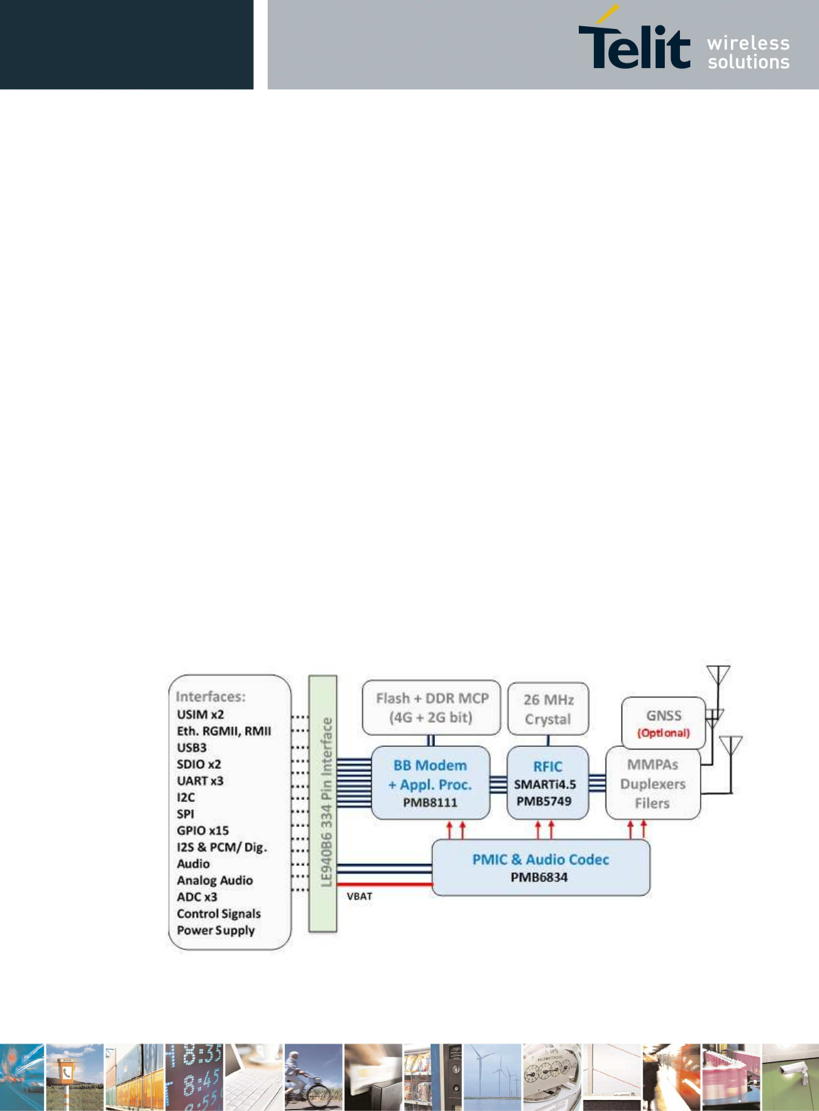
2.3. General Functionality and Main Features
The LE940B6 family of automotive cellular modules features an LTE and multi-RAT modem
together with a powerful on-chip application processor and a rich set of interfaces.
The major functions and features are listed below:
• Multi-RAT with LTE carrier aggregation (Rel. 10, Cat. 6)
• Flash + DDR large enough to allow the space for customer’s own software applications
• Advanced security features
• FOTA (optional)
• Several region variants with optimal choice of RF bands in each for worldwide coverage of
countries and MNOs
• Well-designed form factor (40x40mm), accommodating the multiple RF bands in each region
variant
• Digital audio and analog audio codec
• A GNSS function is not included within the module, but can be supported with the proper
interface while mounted on the customer board
• The entire module is designed by Telit for satisfying the environment and quality
requirements of the automotive market
Figure 1 shows the high-level functionality of the LE940B6 module.
Figure 1: LE940B6 High-level Functionality

LE940B6 Hardware User Guide
1VV0301331 Rev. 1.8 - 2017-03-15
Reproduction forbidden without written authorization by Telit Communications S.p.A. - All Rights Reserved
Telit Confidential Information, provided under NDA Page
19 of 104
2.4. Environmental Requirements
2.4.1. Temperature Range
Operating
temperature range
-20 ~ +55°C.
This range is defined by 3GPP (the global standard for wireless
mobile communication). Telit guarantees its modules to comply with
all the 3GPP requirements and to have full functionality of the
module with in this range.
-40 ~ +85°C.
Telit guarantees full functionality within this range as well. However,
there may possibly be some performance deviations in this
extended range relative to 3GPP requirements, which means that
some RF parameters may deviate from the 3GPP specification in the
order of a few dB. For example: receiver sensitivity or maximum
output power may be slightly degraded.
Even so, all the functionalities, such as call connection, SMS, USB
communication, UART activation etc., will be maintained, and the
effect of such degradations will not lead to malfunction.
–40°C ~ +95°C.
eCall must be functional (until the module is broken)
Storage and non-
operating
temperature range
–40°C ~ +95°C
2.4.2. RoHS Compliance
As a part of the Telit corporate policy of environmental protection, the LE940B6 complies with the
RoHS (Restriction of Hazardous Substances) directive of the European Union (EU directive
2011/65/EU).

LE940B6 Hardware User Guide
1VV0301331 Rev. 1.8 - 2017-03-15
Reproduction forbidden without written authorization by Telit Communications S.p.A. - All Rights Reserved
Telit Confidential Information, provided under NDA Page
20 of 104
2.5. Operating Frequency Bands
The operating frequencies in WCDMA and LTE modes conform to the 3GPP specifications.
2.5.1. RF Bands per Regional Variant
Table 4 summarizes all region variants within the LE940B6 family, showing the supported band
sets in each variant and the supported band pairs for 2x carrier aggregation.
Table 4: RF Bands per Regional Variant
Band 41M for China: 2,555 - 2,655 MHz
Region
Variant
LTE FDD LTE TDD HSPA+ TD-
SCDMA
2G
LE940B6-NA
2, 4, 5, 7, 12, 29(DL) - 2, 4, 5
- 2, 5
LTE Carrier Aggregation 2+5, 2+12, 2+29, 4+4, 4+5, 4+12, 4+29
LE940B6-NV
2, 4, 5, 7, 12, 13, 29(DL) - 2, 4, 5 - 2, 5
LTE Carrier Aggregation 2+5, 2+12, 2+13, 2+29, 4+4, 4+5, 4+12, 4+13, 4+29,
LE940B6-RW
1, 2, 3, 4, 5, 7, 8, 19, 20,
21, 26, 28, 32(DL)
- 1, 2, 3, 4, 5, 8, 19
- 2, 3, 5, 8
LTE Carrier Aggregation 1+5, 1+8, 1+19, 1+21, 1+26, 3+3, 3+5, 3+7, 3+19, 3+20,
3+26, 3+28, 4+4, 7+20, 7+28, 19+21, 20+32
LE940B6-CN
1, 3, 5, 8, 26 38, 39, 40, 41M
1, 3, 5, 8 34, 39 3, 8
LTE Carrier Aggregation 1+26, 3+3, 3+5, 3+26, 39+41, 40+40, 41+41

LE940B6 Hardware User Guide
1VV0301331 Rev. 1.8 - 2017-03-15
Reproduction forbidden without written authorization by Telit Communications S.p.A. - All Rights Reserved
Telit Confidential Information, provided under NDA Page
21 of 104
2.5.2. Reference Table of RF Bands Characteristics
Table 5: RF Bands Characteristics
Mode Freq. Tx (MHz) Freq. Rx (MHz)
Channels Tx-Rx Offset
PCS 1900 1850.2 ~ 1909.8
1930.2 ~ 1989.8
512 ~ 810 80 MHz
DCS 1800 1710.2 ~ 1784.8
1805.2 ~ 1879.8
512 ~ 885 95 MHz
GSM 850 824.2 ~ 848.8 869.2 ~ 893.8 128 ~ 251 45 MHz
EGSM 900 880.2 ~ 914.8 925.2 ~ 959.8 975 ~ 1023, 1 ~ 124
45 MHz
WCDMA 2100 – B1 1920 ~ 1980 2110 ~ 2170 Tx: 9612 ~ 9888
Rx: 10562 ~ 10838
190 MHz
WCDMA 1900 – B2 1850 ~ 1910 1930 ~ 1990 Tx: 9262 ~ 9538
Rx: 9662 ~ 9938
80 MHz
WCDMA 1800 – B3 1710 ~ 1785 1805 ~ 1880 Tx: 937 ~ 1288
Rx: 1162 ~ 1513
95 MHz
WCDMA AWS – B4 1710 ~ 1755 2110 ~ 2155 Tx: 1312 ~ 1513
Rx: 1537 ~ 1738
400 MHz
WCDMA 850 – B5 824 ~ 849 869 ~ 894 Tx: 4132 ~ 4233
Rx: 4357 ~ 4458
45 MHz
WCDMA 900 – B8 880 ~ 915 925 ~ 960 Tx: 2712 ~ 2863
Rx: 2937 ~ 3088
45 MHz
WCDMA 1800 –B9 1750 ~ 1784.8 1845 ~ 1879.8 Tx: 8762 ~ 8912
Rx: 9237 ~ 9387
95 MHz
WCDMA 800 – B19 830 ~ 845 875 ~ 890 Tx: 312 ~ 363
Rx: 712 ~ 763
45 MHz
TDSCDMA 2000 –
B34
2010 ~ 2025 2010 ~ 2025 Tx: 10050 ~ 10125
Rx: 10050 ~ 10125
0 MHz

LE940B6 Hardware User Guide
1VV0301331 Rev. 1.8 - 2017-03-15
Reproduction forbidden without written authorization by Telit Communications S.p.A. - All Rights Reserved
Telit Confidential Information, provided under NDA Page
22 of 104
Mode Freq. Tx (MHz) Freq. Rx (MHz)
Channels Tx-Rx Offset
TDSCDMA 1900 –
B39
1880 ~ 1920 1880 ~ 1920 Tx: 9400 ~ 9600
Rx: 9400 ~ 9600
0 MHz
LTE 2100 – B1 1920 ~ 1980 2110 ~ 2170 Tx: 18000 ~ 18599
Rx: 0 ~ 599
190 MHz
LTE 1900 – B2 1850 ~ 1910 1930 ~ 1990 Tx: 18600 ~ 19199
Rx: 600 ~ 1199
80 MHz
LTE 1800 – B3 1710 ~ 1785 1805 ~ 1880 Tx: 19200 ~ 19949
Rx: 1200 ~ 1949
95 MHz
LTE AWS – B4 1710 ~ 1755 2110 ~ 2155 Tx: 19950 ~ 20399
Rx: 1950 ~ 2399
400 MHz
LTE 850 – B5 824 ~ 849 869 ~ 894 Tx: 20400 ~ 20649
Rx: 2400 ~ 2649
45 MHz
LTE 2600 – B7 2500 ~ 2570 2620 ~ 2690 Tx: 20750 ~ 21449
Rx: 2750 ~ 3449
120 MHz
LTE 900 – B8 880 ~ 915 925 ~ 960 Tx: 21450 ~ 21799
Rx: 3450 ~ 3799
45 MHz
LTE 1800 – B9 1749.9 ~ 1784.9
1844.9 ~ 1879.9
Tx: 21800 ~ 2149
Rx: 3800 ~ 4149
95 MHz
LTE AWS+ – B10 1710 ~ 1770 2110 ~ 2170 Tx: 22150 ~ 22749
Rx: 4150 ~ 4749
400 MHz
LTE 700a – B12 699 ~ 716 729 ~ 746 Tx : 23010 ~ 23179
Rx : 5010 ~ 5179
30 MHz
LTE 700c – B13 777 ~ 787 746 ~ 756 Tx : 23180 ~ 23279
Rx : 5180 ~ 5279
-31 MHz
LTE 700b – B17 704 ~ 716 734 ~ 746 Tx: 23730 ~ 23849
Rx: 5730 ~ 5849
30 MHz

LE940B6 Hardware User Guide
1VV0301331 Rev. 1.8 - 2017-03-15
Reproduction forbidden without written authorization by Telit Communications S.p.A. - All Rights Reserved
Telit Confidential Information, provided under NDA Page
23 of 104
Mode Freq. Tx (MHz) Freq. Rx (MHz)
Channels Tx-Rx Offset
LTE 800 – B19 830 ~ 845 875 ~ 890 Tx: 24000 ~ 24149
Rx: 6000 ~ 6149
45 MHz
LTE 800 – B20 832 ~ 862 791 ~ 821 Tx: 24150 ~ 24449
Rx: 6150 ~ 6449
-41 MHz
LTE 1500 – B21 1447.9 ~ 1462.9
1495.9 ~ 1510.9
Tx: 24450 ~ 24599
Rx: 6450 ~ 6599
48 MHz
LTE 850+ – B26 814 ~ 849 859 ~ 894 Tx: 26690 ~ 27039
Rx: 8690 ~ 9039
45 MHz
LTE 700 – B28 703 ~ 748 758 ~ 803 Tx : 27210 ~ 27659
Rx : 9210 ~ 9659
45 MHz
LTE 700d – B29 Downlink only 717 ~ 728 Rx: 9660 ~ 9769 0 MHz
LTE 1500 – B32 Downlink only 1452 ~ 1496 Rx: 9920 ~ 10359 0 MHz
LTE TDD 2600 – B38
2570 ~ 2620 2570 ~ 2620 Tx: 37750 ~ 38249
Rx: 37750 ~ 38249
0 MHz
LTE TDD 1900 – B39
1880 ~ 1920 1880 ~ 1920 Tx: 38250 ~ 38649
Rx: 38250 ~ 38649
0 MHz
LTE TDD 2300 – B40
2300 ~ 2400 2300 ~ 2400 Tx: 38650 ~ 39649
Rx: 38650 ~ 39649
0 MHz
LTE TDD 2500 – B41
2496 ~ 2690 2496 ~ 2690 Tx: 39650 ~ 41589
Rx: 39650 ~ 41589
0 MHz

LE940B6 Hardware User Guide
1VV0301331 Rev. 1.8 - 2017-03-15
Reproduction forbidden without written authorization by Telit Communications S.p.A. - All Rights Reserved
Telit Confidential Information, provided under NDA Page
24 of 104
2.6. Sensitivity
LE940B6 maximum sensitivity levels are as follows (exact performance figures will be specified at
a later stage):
• < 3GPP @ 2G
• < 3GPP @ 3G
• < 3GPP @ 4G FDD (BW=5 MHz)
• < 3GPP @ 4G TDD (BW=5 MHz)

LE940B6 Hardware User Guide
1VV0301331 Rev. 1.8 - 2017-03-15
Reproduction forbidden without written authorization by Telit Communications S.p.A. - All Rights Reserved
Telit Confidential Information, provided under NDA Page
25 of 104
2.7. LE940B6 Mechanical Specifications
2.7.1. Dimensions
The LE940B6 module’s overall dimensions are:
• Length: 40 mm, +/- 0.20 mm tolerance
• Width: 40 mm, +/- 0.20 mm tolerance
• Thickness: 3.0 mm, +/- 0.15 mm tolerance (with label)
2.7.2. Weight
The nominal weight of the LE940B6 module is 11 gram.

LE940B6 Hardware User Guide
1VV0301331 Rev. 1.8 - 2017-03-15
Reproduction forbidden without written authorization by Telit Communications S.p.A. - All Rights Reserved
Telit Confidential Information, provided under NDA Page
26 of 104
3. LE940B6 Module Connections
3.1. Pin-out
Table 6: LE940B6 Pin-out
PAD Signal I/O
Function Type COMMENT
USB HS 2.0 Communication Port
A18 USB_VBUS AI
Power sense for the internal USB
transceiver
D19 USB_D+ I/O
USB differential Data (+)
F19 USB_D- I/O
USB differential Data (-)
Asynchronous UART
AH19 C103/TXD I Serial data input (TXD) from DTE 1.8V
AF19 C104/RXD O Serial data output (RXD) to DTE 1.8V
AA18 C105/RTS I
Input for Request To Send signal
(RTS) from DTE 1.8V
AK19 C106/CTS O
Output for Clear To Send signal
(CTS) to DTE 1.8V
AG18 C107/DSR O
Output for Data Set Ready signal
(DSR) to DTE 1.8V
AC18 C108/DTR I
Input for Data Terminal Ready
signal (DTR) from DTE 1.8V
AE18 C109/DCD O
Output for
Data Carrier Detect
signal (DCD) to DTE 1.8V
AJ18 C125/RING O
Output for Ring Indicator signal (RI)
to DTE 1.8V
Asynchronous Auxiliary UART
AB19 TXD_AUX O Auxiliary UART (Tx Data to DTE) 1.8V
AD19 RXD_AUX I Auxiliary UART (Rx Data from DTE) 1.8V
Asynchronous UART3
AM9 UART3_TXD I Serial data input (TXD) from DTE 1.8V
AM11
UART3_RXD O Serial data output (RXD) to DTE 1.8V
AM13
UART3_RTS I
Input for Request To Send (RTS)
from DTE 1.8V
AM15
UART3_CTS O
Output for Clear To Send (CTS) to
DTE 1.8V
JTAG – Joint Test Action Group
E4 JTAG_TDI I JTAG_TDI 1.8V
F3 JTAG_RESOUT_N
O JTAG_RESOUT* 1.8V
F5 JTAG_TRIGOUT - JTAG_TRIGOUT 1.8V
G2 JTAG_RTCK O JTAG_RTCK 1.8V
LE940B6 Hardware User Guide
1VV0301331 Rev. 1.8 - 2017-03-15
Reproduction forbidden without written authorization by Telit Communications S.p.A. - All Rights Reserved
Telit Confidential Information, provided under NDA Page
27 of 104
H3 JTAG_TCK I JTAG_TCK 1.8V
J2 JTAG_TRST_N I JTAG_TRST* 1.8V
K3 JTAG_TDO O JTAG_TDO 1.8V
L2 JTAG_TMS I JTAG_TMS 1.8V
M3 JTAG_TRIGIN - JTAG_TRIGIN 1.8V
JTAG - MiPi 34 Interface
L4 JTAG_PTI_CLK O MiPi Clock 1.8V
N4 JTAG_PTI_DATA0
I/O
MiPi Data 0 1.8V
R4 JTAG_PTI_DATA1
I/O
MiPi Data 1 1.8V
T4 JTAG_PTI_DATA2
I/O
MiPi Data 2 1.8V
V4 JTAG_PTI_DATA3
I/O
MiPi Data 3 1.8V
SIM Card Interface
A8 SIMVCC1 -
External SIM signal
–
Power supply
for the SIM 1.8/2.9V
A10 SIMCLK1 O External SIM signal – Clock 1.8/2.9V
B7 SIMIN1 I External SIM signal – Presence 1.8V Active Low
B9 SIMIO1 I/O
External SIM signal – Data I/O 1.8/2.9V
B11 SIMRST1 O External SIM signal – Reset 1.8/2.9V
SIM Card Interface 2
D15 SIMVCC2 -
External SIM signal
–
Power supply
for the SIM 1.8/2.9V
C16 SIMCLK2 O External SIM signal – Clock 1.8/2.9V
C18 SIMIN2 I
External SIM signal
–
Presence
(active low) 1.8V Active Low
E16 SIMIO2 I/O
External SIM signal – Data I/O 1.8/2.9V
D17 SIMRST2 O External SIM signal – Reset 1.8/2.9V
Analog Audio Interface
B5 EAR1_MT+ AO
Earphone signal output, phase +
A4 EAR1_MT- AO
Earphone signal output, phase -
B3 MIC1_MT+ AI
Microphone input, phase +
A2 MIC1_MT- AI
Microphone input, phase -
G6 MIC_BIAS AO
Microphone Bias Power
Digital Voice Interface (DVI)
C8 DVI_RX I Digital Voice interface (Rx) 1.8V
C10 DVI_CLK O
Digital Voice interface (CLK master
output) 1.8V
D9 DVI_TX O Digital Voice interface (Tx) 1.8V
D11 DVI_WA0 O
Digital Voice interface (WA0 master
output) 1.8V
SPI – Serial Peripheral Interface
K19 SPI_MOSI O SPI data Master output Slave input 1.8V
M19 SPI_MISO I SPI data Master input Slave output 1.8V

LE940B6 Hardware User Guide
1VV0301331 Rev. 1.8 - 2017-03-15
Reproduction forbidden without written authorization by Telit Communications S.p.A. - All Rights Reserved
Telit Confidential Information, provided under NDA Page
28 of 104
N18 SPI_CS O SPI Chip select output 1.8V
P19 SPI_CLK O SPI Clock output 1.8V
I2C Interface
C14 I2C_SCL I/O
I2C Clock 1.8V
D13 I2C_SDA I/O
I2C Data 1.8V
Digital I/O
F9 GPIO_01 I/O
GPIO_01 1.8V
E10 GPIO_02 I/O
GPIO_02 1.8V
F11 GPIO_03 I/O
GPIO_03 1.8V
E12 GPIO_04 I/O
GPIO_04 1.8V
F13 GPIO_05 I/O
GPIO_05 1.8V
E14 GPIO_06 I/O
GPIO_06 1.8V
R18 GPIO_07 I/O
GPIO_07 1.8V
S19 GPIO_08 I/O
GPIO_08 1.8V
U19 GPIO_09 I/O
GPIO_09 1.8V
W19 GPIO_10 I/O
GPIO_10 1.8V
L18 GPIO_11 I/O
GPIO_11 1.8V
J18 GPIO_12 I/O
GPIO_12 1.8V
AN4 GPIO_20 I/O
GPIO_20 1.8V
H1 GPIO_21 I/O
GPIO_21 1.8V
K1 GPIO_22 I/O
GPIO_22 1.8V
Analog to Digital Converter
D5 ADC_IN1 AI
Analog to Digital Converter Input 1 Analog
E6 ADC_IN2 AI
Analog to Digital Converter Input 2 Analog
F7 ADC_IN3 AI
Analog to Digital Converter Input 3 Analog
Ethernet MAC/PHY Signals
G14 MAC_MDC O Management Data Clock 2.5/3.3V
G12 MAC_MDIO I/O
Management Data I/O 2.5/3.3V
V16 MAC_TXD[0] O RGMII or RMII TXD[0] 2.5/3.3V
T16 MAC_TXD[1] O RGMII or RMII TXD[1] 2.5/3.3V
R16 MAC_TXD[2] O RGMII TXD[2] 2.5/3.3V
N16 MAC_TXD[3] O RGMII TXD[3] 2.5/3.3V
L16 MAC_GTX_CLK O RGMII Transmit Clock 2.5/3.3V
G16 MAC_TXEN_ER O
RGMII Transmit Enable / Error or
RMII Transmit Enable 2.5/3.3V
AL16 MAC_RXD[0] I RGMII or RMII RXD[0] 2.5/3.3V
AJ16 MAC_RXD[1] I RGMII or RMII RXD[1] 2.5/3.3V
AG16 MAC_RXD[2] I RGMII RXD[2] 2.5/3.3V
AE16 MAC_RXD[3] I RGMII RXD[3] 2.5/3.3V
AC16 MAC_RX_CLK I RGMII Receive Clock 2.5/3.3V

LE940B6 Hardware User Guide
1VV0301331 Rev. 1.8 - 2017-03-15
Reproduction forbidden without written authorization by Telit Communications S.p.A. - All Rights Reserved
Telit Confidential Information, provided under NDA Page
29 of 104
X16 MAC_RXDV_ER I
RGMII Receive Data Available/Error
or RMII Receive Error 2.5/3.3V
G10 ETH_INT_N I Ethernet PHY Interrupt 2.5/3.3V
G8 ETH_RST_N O Ethernet PHY Reset Output 2.5/3.3V
RF Section
AD1 ANT_1 I/O
Primary Antenna 1 RF
AU9 ANT_DIV_1 I Diversity Antenna 1 RF
S1 ANT_GPS I GPS Antenna RF
Miscellaneous Functions
F17 VRTC AI
VRTC Backup capacitor -
K17 VIO_1.8V O VIO_1.8V for reference voltage 1.8V
AN8 RESET_N I Reset Input Active low
AN10 SW_RDY O
Indicates that the boot sequence
completed successfully 1.8V
AN12 SHDN_N I Unconditional Shutdown Input Active low
AS1 ON_OFF_N I Power ON/OFF Input Active low
AU3 STAT_LED O Status Indicator LED 1.8V
P17 VAUX/PWRMON
O
Supply output for external
accessories / Power ON Monitor 1.8V
H17 VPP I Vpp for eFuse
Power Supply
AP17 VBATT - Main Power Supply (Digital Section)
Power
AP19 VBATT - Main Power Supply (Digital Section)
Power
AR18 VBATT - Main Power Supply (Digital Section)
Power
AR20 VBATT - Main Power Supply (Digital Section)
Power
AS17 VBATT_PA -
Main Power Supply (RF Transmit
Power Section) Power
AS19 VBATT_PA -
Ma
in Power Supply (RF Transmit
Power Section) Power
AT18 VBATT_PA -
Main Power Supply (RF Transmit
Power Section) Power
AU17 VBATT_PA -
Main Power Supply (RF Transmit
Power Section) Power
AU19 VBATT_PA -
Main Power Supply (RF Transmit
Power Section) Power
AT20 VBATT_PA -
Main Power Supply (RF Transmit
Power Section) Power
Ground
A6 GND - Ground Ground
A12 GND - Ground Ground
B13 GND - Ground Ground
B15 GND - Ground Ground

LE940B6 Hardware User Guide
1VV0301331 Rev. 1.8 - 2017-03-15
Reproduction forbidden without written authorization by Telit Communications S.p.A. - All Rights Reserved
Telit Confidential Information, provided under NDA Page
30 of 104
B17 GND - Ground Ground
C4 GND - Ground Ground
C6 GND - Ground Ground
D3 GND - Ground Ground
D7 GND - Ground Ground
E18 GND - Ground Ground
F1 GND - Ground Ground
G18 GND - Ground Ground
H19 GND - Ground Ground
M1 GND - Ground Ground
N2 GND - Ground Ground
P1 GND - Ground Ground
P3 GND - Ground Ground
R2 GND - Ground Ground
T2 GND - Ground Ground
T18 GND - Ground Ground
U1 GND - Ground Ground
V18 GND - Ground Ground
W1 GND - Ground Ground
X2 GND - Ground Ground
X18 GND - Ground Ground
Y1 GND - Ground Ground
Y19 GND - Ground Ground
AA2 GND - Ground Ground
AB1 GND - Ground Ground
AC2 GND - Ground Ground
AE2 GND - Ground Ground
AF1 GND - Ground Ground
AG2 GND - Ground Ground
AH1 GND - Ground Ground
AJ2 GND - Ground Ground
AK1 GND - Ground Ground
AK17 GND - Ground Ground
AL18 GND - Ground Ground
AM17
GND - Ground Ground
AM19
GND - Ground Ground
AN16 GND - Ground Ground
AN18 GND - Ground Ground
AP3 GND - Ground Ground
AP5 GND - Ground Ground

LE940B6 Hardware User Guide
1VV0301331 Rev. 1.8 - 2017-03-15
Reproduction forbidden without written authorization by Telit Communications S.p.A. - All Rights Reserved
Telit Confidential Information, provided under NDA Page
31 of 104
AP7 GND - Ground Ground
AP9 GND - Ground Ground
AP11 GND - Ground Ground
AP13 GND - Ground Ground
AP15 GND - Ground Ground
AR2 GND - Ground Ground
AR4 GND - Ground Ground
AR6 GND - Ground Ground
AR8 GND - Ground Ground
AR10 GND - Ground Ground
AR12 GND - Ground Ground
AR14 GND - Ground Ground
AR16 GND - Ground Ground
AS5 GND - Ground Ground
AS7 GND - Ground Ground
AS9 GND - Ground Ground
AS11 GND - Ground Ground
AS13 GND - Ground Ground
AS15 GND - Ground Ground
AT4 GND - Ground Ground
AT6 GND - Ground Ground
AT8 GND - Ground Ground
AT10 GND - Ground Ground
AT12 GND - Ground Ground
AT14 GND - Ground Ground
AT16 GND - Ground Ground
AU1 GND - Ground Ground
AU5 GND - Ground Ground
AU7 GND - Ground Ground
AU11 GND - Ground Ground
AU15 GND - Ground Ground
AL2 GND - Ground Ground
AN2 GND - Ground Ground
L20 GND - Ground Ground
N20 GND - Ground Ground
ZZ19 GND - Ground Ground
A20 GND - Ground Ground
AV20 GND - Ground Ground
ZZ1 GND - Ground Ground
A0 GND - Ground Ground

LE940B6 Hardware User Guide
1VV0301331 Rev. 1.8 - 2017-03-15
Reproduction forbidden without written authorization by Telit Communications S.p.A. - All Rights Reserved
Telit Confidential Information, provided under NDA Page
32 of 104
AV0 GND - Ground Ground
N0 GND - Ground Ground
R0 GND - Ground Ground
T0 GND - Ground Ground
V0 GND - Ground Ground
X0 GND - Ground Ground
AA0 GND - Ground Ground
AC0 GND - Ground Ground
AE0 GND - Ground Ground
AG0 GND - Ground Ground
AJ0 GND - Ground Ground
AL0 GND - Ground Ground
AN0 GND - Ground Ground
AR0 GND - Ground Ground
AV8 GND - Ground Ground
AV10 GND - Ground Ground
AV12 GND - Ground Ground
AV14 GND - Ground Ground
AV16 GND - Ground Ground
AV18 GND - Ground Ground
T8 GND - Ground Ground
V8 GND - Ground Ground
X8 GND - Ground Ground
AA8 GND - Ground Ground
U9 GND - Ground Ground
W9 GND - Ground Ground
Y9 GND - Ground Ground
T10 GND - Ground Ground
V10 GND - Ground Ground
X10 GND - Ground Ground
AA10 GND - Ground Ground
U11 GND - Ground Ground
W11 GND - Ground Ground
Y11 GND - Ground Ground
T12 GND - Ground Ground
V12 GND - Ground Ground
X12 GND - Ground Ground
AA12 GND - Ground Ground
ZZ101
GND - Ground Ground
B101 GND - Ground Ground

LE940B6 Hardware User Guide
1VV0301331 Rev. 1.8 - 2017-03-15
Reproduction forbidden without written authorization by Telit Communications S.p.A. - All Rights Reserved
Telit Confidential Information, provided under NDA Page
33 of 104
D101 GND - Ground Ground
U101 GND - Ground Ground
W101
GND - Ground Ground
Y101 GND - Ground Ground
AR101
GND - Ground Ground
AT101
GND - Ground Ground
AV101
GND - Ground Ground
ZZ102
GND - Ground Ground
B102 GND - Ground Ground
D102 GND - Ground Ground
U102 GND - Ground Ground
W102
GND - Ground Ground
Y102 GND - Ground Ground
AR102
GND - Ground Ground
AT102
GND - Ground Ground
AV102
GND - Ground Ground
Reserved
B19 Reserved - Reserved
C20 Reserved - Reserved
E20 Reserved - Reserved
G20 Reserved - Reserved
J20 Reserved - Reserved
AN14 Reserved - Reserved
E8 Reserved - Reserved
E2 Reserved - Reserved
D1 Reserved - Reserved
C2 Reserved - Reserved
B1 Reserved - Reserved
C12 Reserved - Reserved
J4 Reserved - Reserved
G4 Reserved - Reserved
AE4 Reserved - Reserved
AC4 Reserved - Reserved
Y3 Reserved - Reserved
AB3 Reserved - Reserved
AD3 Reserved - Reserved
AF3 Reserved - Reserved
AH3 Reserved - Reserved
AK3 Reserved - Reserved
AM3 Reserved - Reserved

LE940B6 Hardware User Guide
1VV0301331 Rev. 1.8 - 2017-03-15
Reproduction forbidden without written authorization by Telit Communications S.p.A. - All Rights Reserved
Telit Confidential Information, provided under NDA Page
34 of 104
AG4 Reserved - Reserved
AJ4 Reserved - Reserved
AL4 Reserved - Reserved
AM5 Reserved - Reserved
X4 Reserved - Reserved
AA4 Reserved - Reserved
S17 Reserved - Reserved
U17 Reserved - Reserved
AH17 Reserved - Reserved
Y17 Reserved - Reserved
AF17 Reserved - Reserved
AB17 Reserved - Reserved
W17 Reserved - Reserved
AD17 Reserved - Reserved
R20 Reserved - Reserved
T20 Reserved - Reserved
V20 Reserved - Reserved
X20 Reserved - Reserved
AA20 Reserved - Reserved
AC20 Reserved - Reserved
AE20 Reserved - Reserved
AG20 Reserved - Reserved
AJ20 Reserved - Reserved
AA16 Reserved - Reserved
J16 Reserved - Reserved
ZZ11 Reserved - Reserved
ZZ13 Reserved - Reserved
ZZ15 Reserved - Reserved
ZZ17 Reserved - Reserved
ZZ9 Reserved - Reserved
ZZ7 Reserved - Reserved
ZZ5 Reserved - Reserved
ZZ3 Reserved - Reserved
C0 Reserved - Reserved
E0 Reserved - Reserved
G0 Reserved - Reserved
J0 Reserved - Reserved
AM1 Reserved - Reserved
AU13 Reserved - Reserved
V2 Reserved - Reserved
LE940B6 Hardware User Guide
1VV0301331 Rev. 1.8 - 2017-03-15
Reproduction forbidden without written authorization by Telit Communications S.p.A. - All Rights Reserved
Telit Confidential Information, provided under NDA Page
35 of 104
W3 Reserved - Reserved
A14 Reserved - Reserved
A16 Reserved - Reserved
F15 Reserved - Reserved
AP1 Reserved - Reserved
M17 Reserved - Reserved
AN6 Reserved - Reserved
AS3 Reserved - Reserved
AT2 Reserved - Reserved
S3 Reserved - Reserved
U3 Reserved - Reserved
L0 Reserved - Reserved
AM7 Reserved - Reserved
AL20 Reserved - Reserved
AN20 Reserved - Reserved
AT0 Reserved - Reserved
AV6 Reserved - Reserved
AV2 Reserved - Reserved
AV4 Reserved - Reserved
NOTE:
When the UART signals are used as the communication port between the host and the
modem:
• The DTR pin must be connected to enter LE940B6 power saving mode.
• The RI pin must be connected to wake up the host when a call is coming while the host
is in Sleep mode.
• The RTS must be connected to GND (on the module side) if flow control is not used.
If the UART port is not used, all UART signals can be left disconnected.
NOTE:
Unless otherwise specified, RESERVED pins must be left unconnected (floating).
The only exceptions are in the following Section: 3.2 LE940B6 Signals That Must Be Connected.

LE940B6 Hardware User Guide
1VV0301331 Rev. 1.8 - 2017-03-15
Reproduction forbidden without written authorization by Telit Communications S.p.A. - All Rights Reserved
Telit Confidential Information, provided under NDA Page
36 of 104
3.2. LE940B6 Signals That Must Be Connected
Table 7 lists the LE940B6 signals that must be connected even if not used by the end application:
Table 7: Mandatory Signals
PAD Signal Notes
AP17, AP19, AR18, AR20, AS17, AS19, AT18,
AU17, AU19, AT20
VBATT &
VBATT_PA
A6, A12, B13, B15, B17, C4, C6, D3, D7, E18,
F1, G18, H19, M1, N2, P1, P3, R2, T2, T18, U1,
V18, W1, X2, X18, Y1, Y19, AA2, AB1, AC2, AE2,
AF1, AG2, AH1, AJ2, AK1, AK17, AL18, AM17,
AM19, AN16, AN18, AP3, AP5, AP7, AP9, AP11,
AP13, AP15, AR2, AR4, AR6, AR8, AR10, AR12,
AR14, AR16, AS5, AS7, AS9, AS11, AS13, AS15,
AT4, AT6, AT8, AT10, AT12, AT14, AT16, AU1,
AU5, AU7, AU11, AU15, AL2, AN2, L20, N20,
ZZ19, A20, AV20, ZZ1, A0, AV0, N0, R0, T0, V0,
X0, AA0, AC0, AE0, AG0, AJ0, AL0, AN0, AR0,
AV8, AV10, AV12, AV14, AV16, AV18, T8, V8,
X8, AA8, U9, W9, Y9, T10 ,V10, X10, AA10,
U11, W11, Y11, T12, V12, X12, AA12
GND
AS1 ON/OFF*
AN12 SHDN_N
D19 USB_D+ If not used, connect to a test
point or a USB connector
F19 USB_D- If not used, connect to a test
point or a USB connector
A18 USB_VBUS If not used, connect to a test
point or a USB connector
C20 USB_SS_RX_P
If not used, connect to a test
point or a USB connector
E20 USB_SS_RX_M
If not used, connect to a test
point or a USB connector
G20 USB_SS_TX_P
If not used, connect to a test
point or a USB connector

LE940B6 Hardware User Guide
1VV0301331 Rev. 1.8 - 2017-03-15
Reproduction forbidden without written authorization by Telit Communications S.p.A. - All Rights Reserved
Telit Confidential Information, provided under NDA Page
37 of 104
J20 USB_SS_TX_M
If not used, connect to a test
point or a USB connector
AH19 C103/TXD If not used, connect to a test
point
AF19 C104/RXD If not used, connect to a test
point
AA18 C105/RTS If flow control is not used,
connect to GND
AK19 C106/CTS If not used, connect to a test
point
AB19 TXD_AUX If not used, connect to a test
point
AD19 RXD_AUX If not used, connect to a test
point
AD1 ANT_1 If not used, connect to a 50 Ohm
termination
AU9 ANT_DIV_1 If not used, connect to a 50 Ohm
termination
S1 ANT_GPS If not used, connect to a 50 Ohm
termination
E4, F3, F5, G2, H3, J2, K3, L2, M3, L4, N4, R4,
T4, V4 For Analysis
Recommended to connect to
test
points for analysis
LE940B6 Hardware User Guide
1VV0301331 Rev. 1.8 - 2017-03-15
Reproduction forbidden without written authorization by Telit Communications S.p.A. - All Rights Reserved
Telit Confidential Information, provided under NDA Page
38 of 104
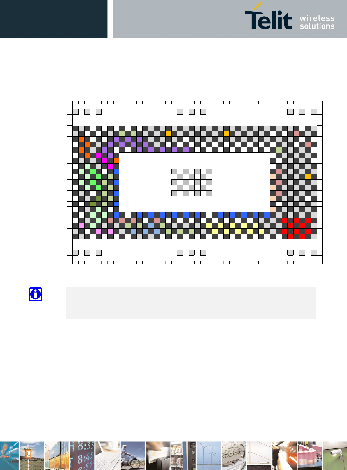
3.3. LGA Pads Layout
Figure 2: LGA Pads Layout LE940B6 334 Pads Top View
(*) MMC is not supported, and the pins assigned for it became Reserved
NOTE:
The pin defined as RFU must be considered RESERVED and not connected to any pin in the
application. The related area on the application must be kept empty.
ZZ A B C D E F G H J K L M N P R S T U V W X Y AA AB AC AD AE AF AG AH AJ AK AL AM AN AP AR AS AT AU AV
101
GND GND GN D GND GND GND GND GND GN D
101
0
GND RFU RFU RFU RFU RFU GND GND GND GND GND GND GND GND GND GND GND GND GND RFU GND
0
1
GND RFU RFU GND GPIO_2
1
GPIO_2
2GND GND ANT_GP
SGND GND GND GND ANT_1 GND GND GND RFU RFU ON_OFF
_N GND
1
2
MIC1_M
T- RFU RFU JTAG_R
TCK
JTAG_T
RST_N
JTAG_T
MS GND GND GND RFU GND GND GND GND GND GND GND GND GND RFU RFU
2
3
RFU MIC1_M
T+ GND
JTAG_R
ESOUT_
N
JTAG_T
CK
JTAG_T
DO
JTAG_T
RIGIN GND RFU RFU RFU RFU RFU RFU RFU RFU RFU RFU GND RFU ST AT_L
ED
3
4
EAR1_M
T- GND JTAG_T
DI RFU RFU JTAG_P
TI_CLK
JTAG_P
TI_DAT
A0
JTAG_P
TI_DAT
A1
JTAG_P
TI_DAT
A2
JTAG_P
TI_DAT
A3
RFU RFU RFU RFU RFU RFU RFU GPIO_2
0GND GND RFU
4
5
RFU EAR1_M
T+
ADC_IN
1
JTAG_T
RIGOUT RFU GND GND GND
5
6
GND GND ADC_IN
2
MIC_BIA
SRFU GND GND RFU
6
7
RFU SIMIN1 GND ADC_IN
3RFU GND GND GND
7
8
SIMVCC
1DVI_RX RFU ETH_RS
T_N GND GND GND GND RESET_
NGND GND GND
8
9
RFU SIMIO1 DVI_TX GPIO_0
1GND GND GND UART3_
TXD GND GND ANT_DI
V_1
9
10
SIMCLK
1
DVI_CL
K
GPIO_0
2
ETH_IN
T_N GND GND GND GND SW_RDY GND GND GND
10
11
RFU SIMRST
1
DVI_WA
0
GPIO_0
3GND GND GND UART3_
RXD GND GND GND
11
12
GND RFU GPIO_0
4
MAC_MD
IO GND GND GND GND SHDN_N GND GND GND
12
13
RFU GND I2C_SDA GPIO_0
5
UART3_
RTS GND GND RFU
13
14
RFU I2C_SCL GPIO_0
6
MAC_MD
CRFU GND GND GND
14
15
RFU GND SIMVCC
2RFU UART3_
CTS GND GND GND
15
16
RFU SIMCLK
2SIMIO2 MAC_TX
EN_ER RFU MAC_GT
X_CLK
MAC_TX
D[3]
MAC_TX
D[2]
MAC_TX
D[1]
MAC_TX
D[0]
MAC_RX
DV_ER RFU MAC_RX
_CLK
MAC_RX
D[3]
MAC_RX
D[2]
MAC_RX
D[1]
MAC_RX
D[0] GND GND GND GND
16
17
RFU GND SIMRST
2VRTC VPP VIO _1.8
VRFU VAUX/P
WRMON RFU RFU RFU RFU RFU RFU RFU RFU GND GND VBATT VBATT_
PA
VBATT_
PA
17
18
USB_VB
US SIMIN2 GND GND GPIO_1
2
GPIO_1
1SPI_CS GP IO_0
7GND GND GND C105/RT
S
C108/DT
R
C109/DC
D
C107/DS
R
C125/RI
NG GND GND VBATT VBATT_
PA GND
18
19
GND RFU USB_D+ USB_D- GND SPI _MO
SI
SPI_ MIS
O
SPI_CL
K
GPIO_0
8
GPIO_0
9
GPIO_1
0GND TXD_AU
X
RXD_AU
X
C104/RX
D
C103/TX
D
C106/CT
SGND VBATT VBATT_
PA
VBATT_
PA
19
20
GND RFU RFU RFU RFU GND GND RFU RFU RFU RFU RFU RFU RFU RFU RFU RFU RFU VBATT VBATT_
PA GND
20
102
GND GND GN D GND GND GND GND GND GN D
102
ZZ A B C D E F G H J K L M N P R S T U V W X Y AA AB AC AD AE AF AG AH AJ AK AL AM AN AP AR AS AT AU AV
LE940B6 (40 mm X 40 mm) Form Factor Pin MAP
TOP VIEW
LE940B6 Hardware User Guide
1VV0301331 Rev. 1.8 - 2017-03-15
Reproduction forbidden without written authorization by Telit Communications S.p.A. - All Rights Reserved
Telit Confidential Information, provided under NDA Page
39 of 104
4. Electrical Specifications
4.1. Absolute Maximum Ratings – Not Operational
Caution:
A deviation from the value ranges listed below may harm the LE940B6 module.
Table 8: Absolute Maximum Ratings – Not Operational
Symbol Parameter Min Max Unit
VBATT Battery supply voltage on pin VBATT -0.3 +6.0 [V]
VBATT_PA Battery supply voltage on pin VBATT_PA -0.3 +6.0 [V]
4.2. Recommended Operating Conditions
Table 9: Recommended Operating Conditions
Symbol Parameter Min Typ Max Unit
T
amb
Ambient temperature -40 +25 +85 [°C]
VBATT Battery supply voltage on pin
VBATT
3.4 3.8 4.2 [V]
VBATT_PA Battery supply voltage on pin
VBATT_PA
3.4 3.8 4.2 [V]
I
BATT_PA +
I
BATT
Peak current to be used to
dimension decoupling
capacitors on pin VBATT_PA
- 80 2000 [mA]
LE940B6 Hardware User Guide
1VV0301331 Rev. 1.8 - 2017-03-15
Reproduction forbidden without written authorization by Telit Communications S.p.A. - All Rights Reserved
Telit Confidential Information, provided under NDA Page
40 of 104
4.3. Logic Level Specifications
Unless otherwise specified, all the interface circuits of the LE940B6 are 1.8V CMOS logic.
Only few specific interfaces (such as MAC, USIM and SD Card) are capable of dual voltage I/O.
The following tables show the logic level specifications used in the LE940B6 interface circuits. The
data specified in the tables below is valid throughout all drive strengths and the entire
temperature ranges.
NOTE:
Do not connect LE940B6 digital logic signals directly to OEM digital logic signals with a level
higher than 2.7V for 1.8V CMOS signals.
4.3.1. 1.8V Standard GPIOs
Table 10: Absolute Maximum Ratings – Not Functional
Parameter Min Max
Input level on standard GPIOs when on
-0.3V +2.3V
Table 11: Operating Range – Interface Levels (1.8V CMOS)
Parameter Min Max
Input high level 1.26V 2.0V
Input low level -0.2V 0.36V
Output high level 1.6V ---
Output low level --- 0.2V

LE940B6 Hardware User Guide
1VV0301331 Rev. 1.8 - 2017-03-15
Reproduction forbidden without written authorization by Telit Communications S.p.A. - All Rights Reserved
Telit Confidential Information, provided under NDA Page
41 of 104
4.3.2. 1.8V I2C Pads
Table 12: Operating Range – 1.8V I2C Pads
Parameter Min Max
Input high level 1.26V 2.3V
Input low level -0.3V 0.54V
Output high level --- ---
Output low level --- 0.36V
4.3.3. 1.2V EMIC Pads
Table 13: Operating Range – 1.2V EMIC Pads
Parameter Min Max
Input high level 0.84V 1.4V
Input low level -0.2V 0.24V
Output high level 1.0V ---
Output low level --- 0.2V
LE940B6 Hardware User Guide
1VV0301331 Rev. 1.8 - 2017-03-15
Reproduction forbidden without written authorization by Telit Communications S.p.A. - All Rights Reserved
Telit Confidential Information, provided under NDA Page
42 of 104
4.3.4. 1.8V/2.9V SIM Pads
Table 14: Operating Range – 1.8V SIM Pads
Parameter Min Max
Input high level 1.26V 2.1V
Input low level -0.3V 0.36V
Output high level 1.26V 2.1V
Output low level -0.3V 0.36V
Table 15: Operating Range – 2.9V SIM Pads
Parameter Min Max
Input high level 2.03V 3.1V
Input low level -0.3V 0.58V
Output high level 2.03V 3.1V
Output low level -0.3V 0.58V
4.3.5. USB
Table 16: Operating Range – USB_D+, USB_D- Pads
Parameter Min Max
Input high level 2.0V ---
Input low level --- 0.8V
Output high level 2.8V ---
Output low level --- 0.3V

LE940B6 Hardware User Guide
1VV0301331 Rev. 1.8 - 2017-03-15
Reproduction forbidden without written authorization by Telit Communications S.p.A. - All Rights Reserved
Telit Confidential Information, provided under NDA Page
43 of 104
4.3.6. 2.5V/3.3V EMAC Interface for RMII and RGMII
Table 17: Absolute Maximum Ratings – 3.3V EMAC Interface
Parameter Min Max
Input level on 3.3V EMAC when on -0.3V 3.6V
Table 18: Operating Range – 2.5V EMAC Interface
Parameter Min Max
Input high level 1.7V 2.5V
Input low level -0.3V 0.7V
Output high level 2V ---
Output low level --- 0.4V
Table 19: Operating Range – 3.3V EMAC Interface
Parameter Min Max
Input high level 2V 3.3V
Input low level -0.3V 0.8V
Output high level 2.6V ---
Output low level --- 0.5V
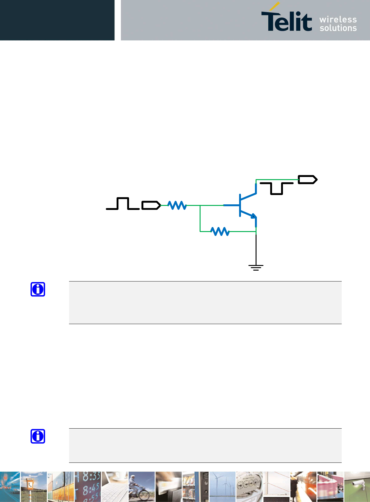
LE940B6 Hardware User Guide
1VV0301331 Rev. 1.8 - 2017-03-15
Reproduction forbidden without written authorization by Telit Communications S.p.A. - All Rights Reserved
Telit Confidential Information, provided under NDA Page
44 of 104
5. Hardware Commands
5.1. Turning on the LE940B6 Module
To turn on the LE940B6 module, the ON_OFF_N pad must be asserted low in the range of 80 - 120
milliseconds and then released.
Figure 3 illustrates a simple circuit to power on the module using an inverted buffer output.
Figure 3: Power-on Circuit
GND
R1
R2
Q1
Power ON Impulse
80ms < Hold Time < 120ms
ON_OFF_N
NOTE:
In case VBATT need to be removed and applied again. The application must take into account the
decay time of the power supply after removal of VBATT. VBATT input must be at zero volt prior
to the reapplication of VBATT."
5.2. Initialization and Activation State
After turning on the LE940B6 module, a predefined internal boot sequence performs the HW and
SW initialization of the module, which takes some time to fully complete. During this process, the
LE940B6 is not accessible.
As shown in Figure 4, the LE940B6 becomes operational at least 25 seconds after PWRMON goes
HIGH.
NOTE:
During the Initialization state, AT commands are not available. The DTE host must wait for the
Activation state prior to communicating with the LE940B6.
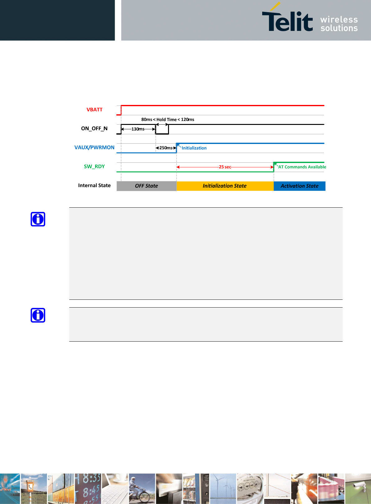
LE940B6 Hardware User Guide
1VV0301331 Rev. 1.8 - 2017-03-15
Reproduction forbidden without written authorization by Telit Communications S.p.A. - All Rights Reserved
Telit Confidential Information, provided under NDA Page
45 of 104
Figure 4: LE940B6 Initialization and Activation
NOTE:
To check whether the LE940B6 has completely powered on, monitor the SW_RDY hardware line.
When SW_RDY goes high, the module has completely powered on and is ready to accept AT
commands.
NOTE:
Do not use any pull-up resistor on the ON_OFF_N line as it is internally pulled up. Using a pull-up
resistor may cause latch-up problems on the LE940B6 power regulator and improper powering
on/off of the module. The ON_OFF_N line must be connected only in an open-collector
configuration.
NOTE:
To avoid a back-powering effect, it is recommended to avoid having any HIGH logic level signal
applied to the digital pins of the module when it is powered OFF or during an ON/OFF transition.
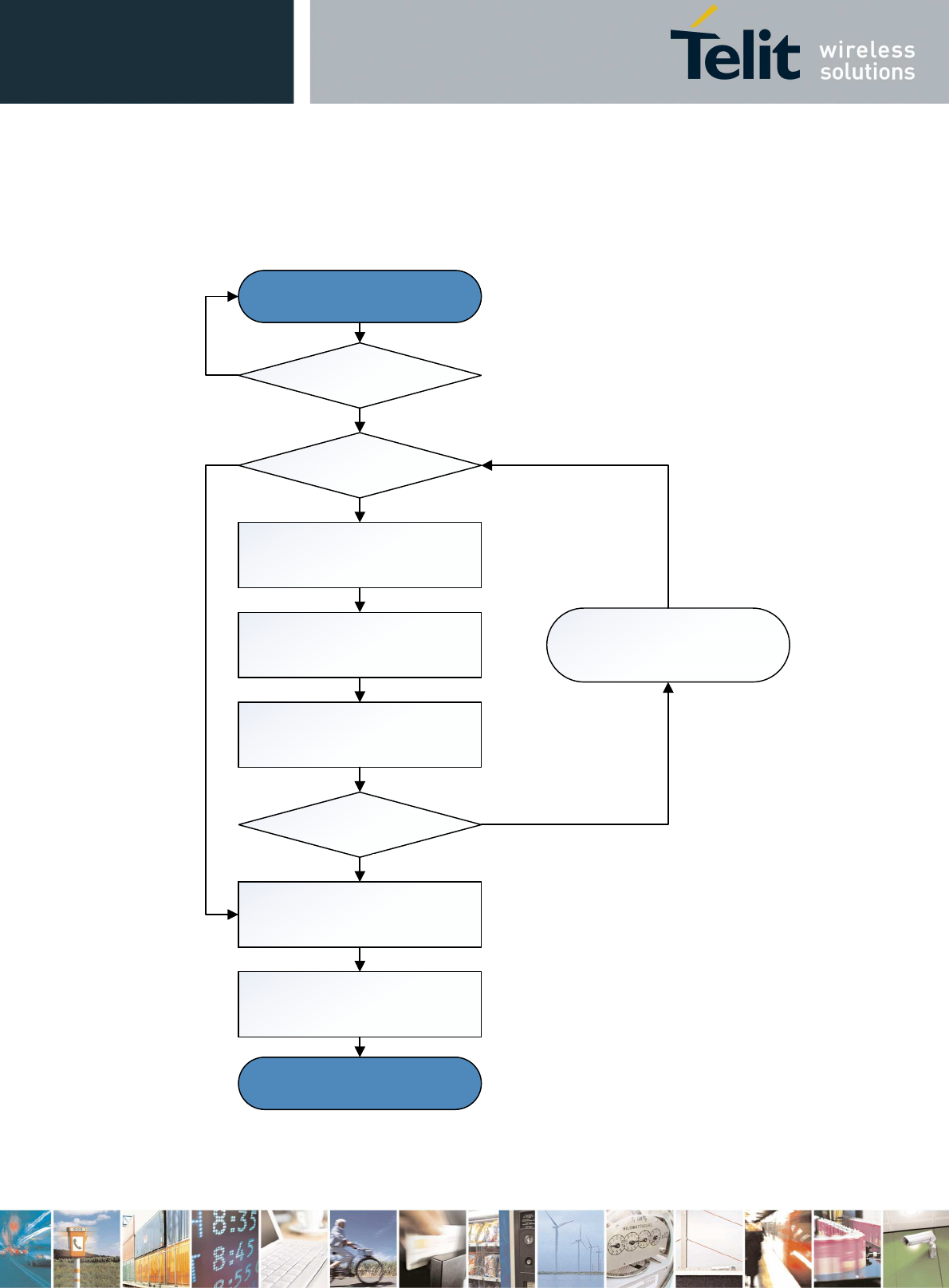
LE940B6 Hardware User Guide
1VV0301331 Rev. 1.8 - 2017-03-15
Reproduction forbidden without written authorization by Telit Communications S.p.A. - All Rights Reserved
Telit Confidential Information, provided under NDA Page
46 of 104
Figure 5 shows a flow chart for the proper power-up procedure:
Figure 5: Power-up Flow Chart
Modem ON Procedure
START
VBATT > 3.4V ?
VAUX/PWRMON = ON?
ON_OFF_N = LOW
80 ms < Hold Time < 120 ms
ON_OFF_N = HIGH
VAUX/PWRMON = ON?
Delay = 25 sec
Go to
Start AT CMD
Modem ON Procedure
END
N
Y
Y
N
Go to
HW SHUTDOWN
Unconditional
N
Y
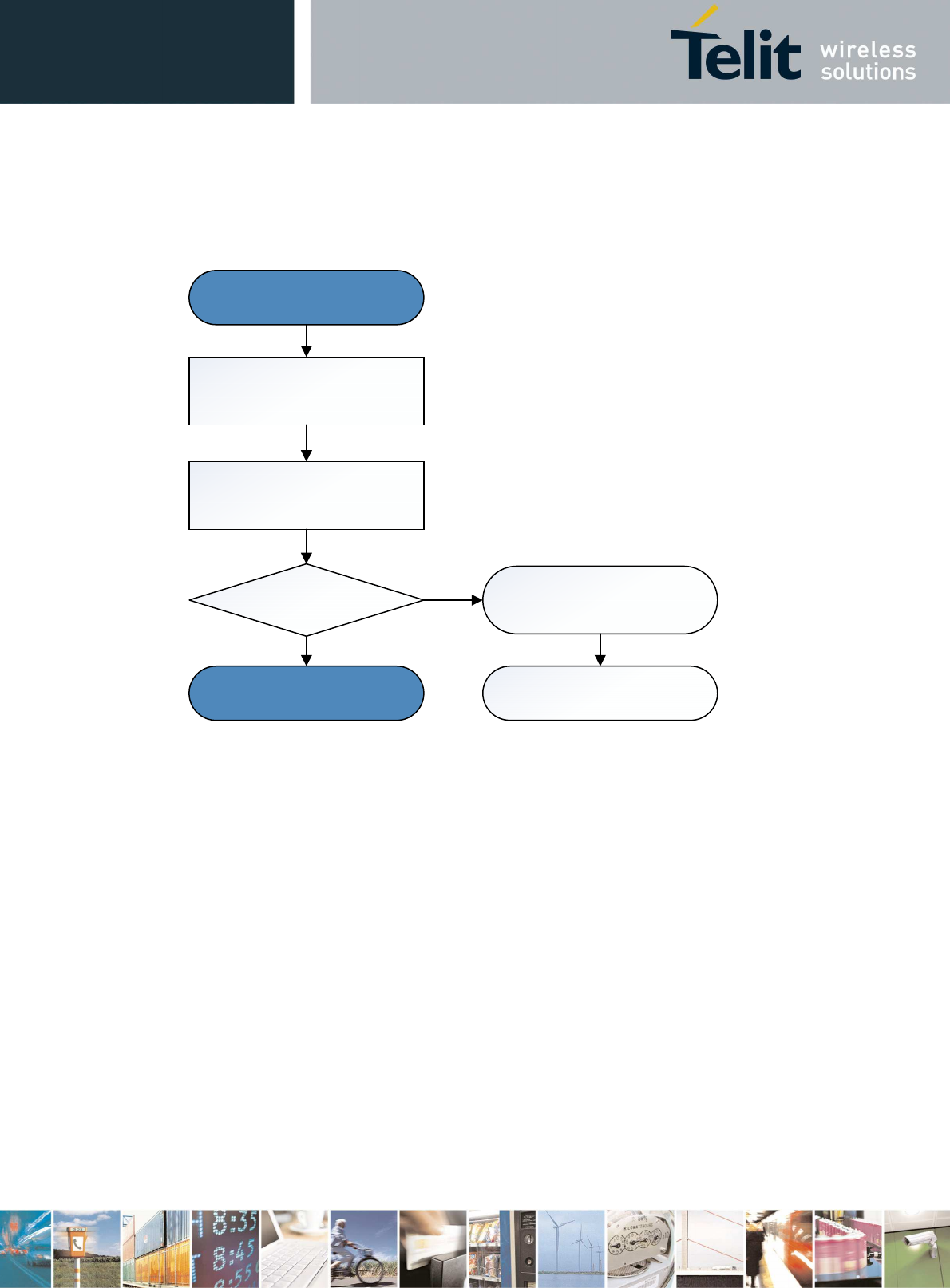
LE940B6 Hardware User Guide
1VV0301331 Rev. 1.8 - 2017-03-15
Reproduction forbidden without written authorization by Telit Communications S.p.A. - All Rights Reserved
Telit Confidential Information, provided under NDA Page
47 of 104
Figure 6 shows a flow chart illustrating the AT commands managing procedure.
Figure 6: AT Command Managing Flow Chart
Start AT CMD
START
Delay 300 ms
Enter AT <CR>
AT Answer in
1 sec ?
Start AT CMD
END
Y
Go to
Modem ON Procedure
Go to
HW SHUTDOWN
Undonditional
N
LE940B6 Hardware User Guide
1VV0301331 Rev. 1.8 - 2017-03-15
Reproduction forbidden without written authorization by Telit Communications S.p.A. - All Rights Reserved
Telit Confidential Information, provided under NDA Page
48 of 104
5.3. Turning off the LE940B6 Module
Turning off the device can be done in four different ways:
• Shutdown by software command using AT#SHDN command
• Hardware shutdown using ON_OFF_N pad
• Hardware Unconditional Reset using the RESET_N pad
• Hardware Unconditional Shutdown using the SHDN_N pad
When the device is shut down by a software command or a hardware shutdown, it issues a
detach request to the network, informing the network that the device will not be reachable any
more.
NOTE:
To check if the device has powered off, monitor the VAUX/PWRMON hardware line. When
VAUX/PWRMON goes low, this indicates that the device has powered off.
NOTE:
To avoid a back-powering effect, it is recommended to avoid having any HIGH logic level signal
applied to the digital pins of the module when it is powered OFF or during an ON/OFF transition.
NOTE:
VBATT must be never removed before the proper OFF procedure is performed.
NOTE:
In case VBATT need to be removed and applied again. The application must take into account the
decay time of the power supply after removal of VBATT. VBATT input must be at zero volt prior
to the reapplication of VBATT.”
5.3.1. Shutdown by Software Command
The LE940B6 module can be shut down by a software command.
When a shutdown command is sent, LE940B6 goes into the Finalization state and at the end of
the finalization process shuts down VAUX/PWRMON.
The duration of the Finalization state can differ according to the current situation of the module,
so a value cannot be defined.
Usually, it will take more than 6 seconds from sending a shutdown command until reaching a
complete shutdown. The DTE host should monitor the status of VAUX/PWRMON to observe the
actual power-off.
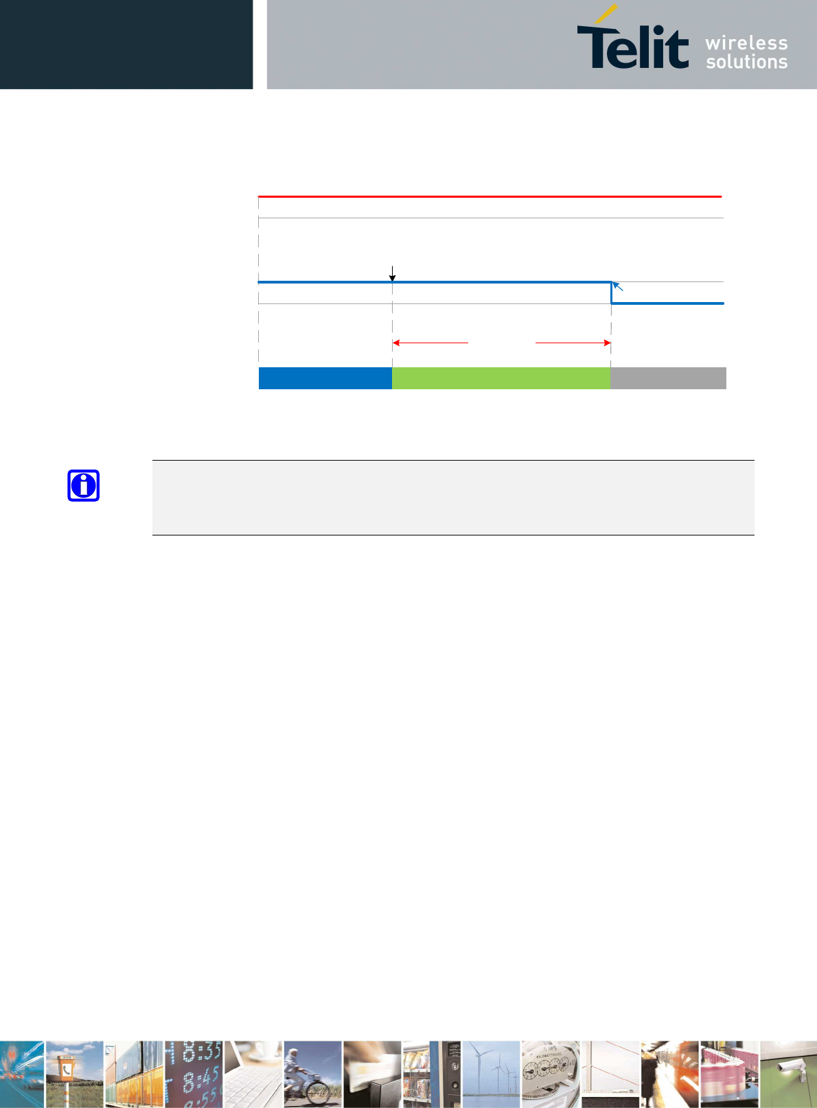
LE940B6 Hardware User Guide
1VV0301331 Rev. 1.8 - 2017-03-15
Reproduction forbidden without written authorization by Telit Communications S.p.A. - All Rights Reserved
Telit Confidential Information, provided under NDA Page
49 of 104
Figure 7: Shutdown by Software Command
Finalization State OFF State
Internal State
VAUX/PWRMON
VBATT
Activation State
AT#SHDN
Variable Above
6 sec
Monitoring Status
NOTE:
To check whether the device has powered off, monitor the VAUX/PWRMON hardware line.
When VAUX/PWRMON goes low, the device has powered off.
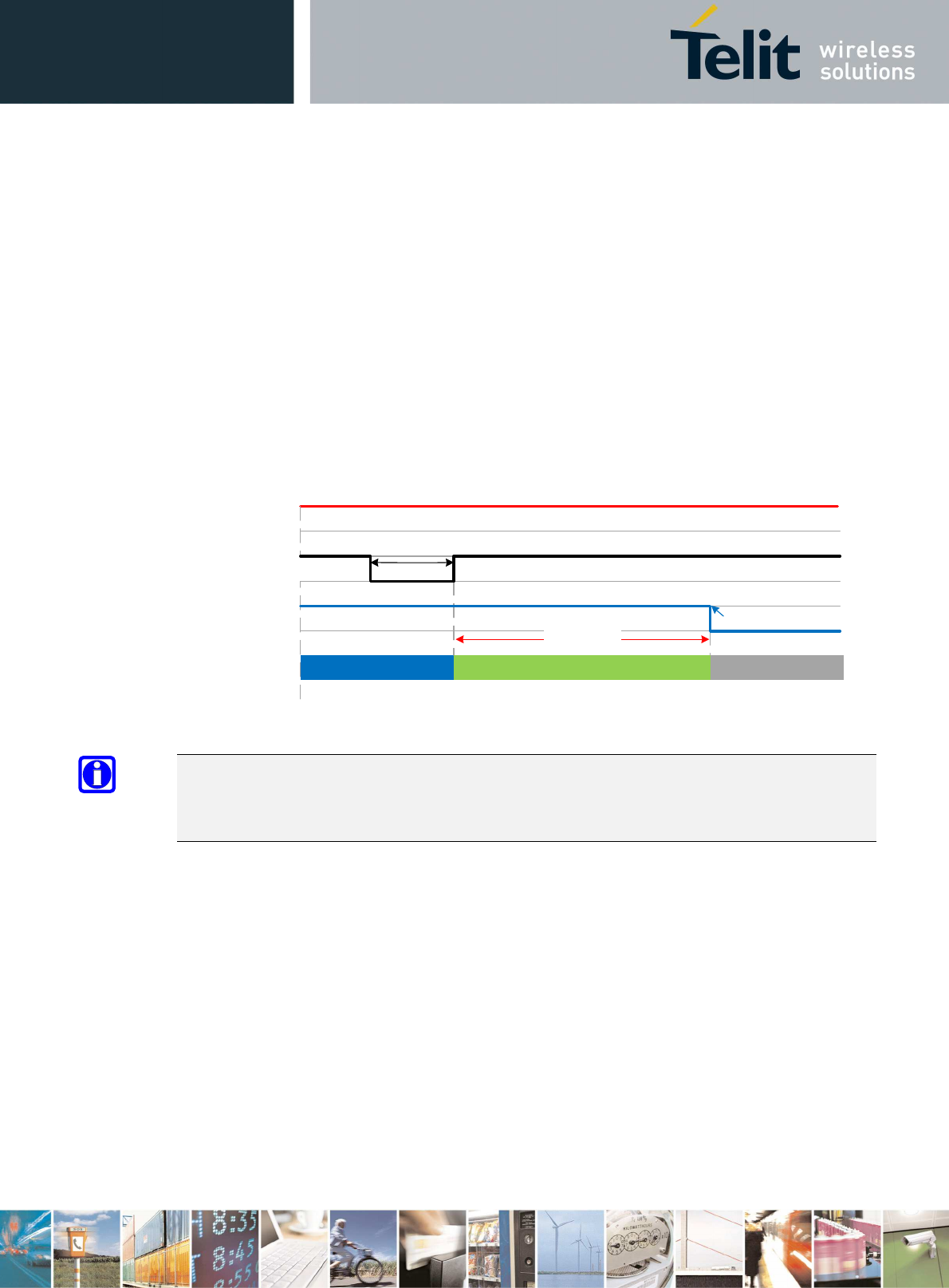
LE940B6 Hardware User Guide
1VV0301331 Rev. 1.8 - 2017-03-15
Reproduction forbidden without written authorization by Telit Communications S.p.A. - All Rights Reserved
Telit Confidential Information, provided under NDA Page
50 of 104
5.3.2. Hardware Shutdown
To turn off the LE940B6 module, the ON_OFF_N pad must be asserted low in the range of 1150 -
1250 milliseconds and then released. Use the same circuitry and timing for power-on.
When the ON_OFF_N is asserted low for a period in the range 1150 - 1250 milliseconds and then
released, LE940B6 goes into the Finalization state and in the end shuts down VAUX/PWRMON.
The duration of the Finalization state can differ according to the current situation of the module,
so a value cannot be defined.
Usually, it will take more than 6 seconds from sending a shutdown command until reaching a
complete shutdown. The DTE host should monitor the status of VAUX/PWRMON to observe the
actual power-off.
Figure 8: Hardware Shutdown
OFF State
Internal State
VAUX/PWRMON
VBATT
Activation State
Variable Above
6 sec
Monitoring Status
ON_OFF_N
1150ms < Hold Time < 1250ms
Finalization State
NOTE:
To check whether the device has powered off, monitor the VAUX/PWRMON hardware line.
When VAUX/PWRMON goes low, the device has powered off.
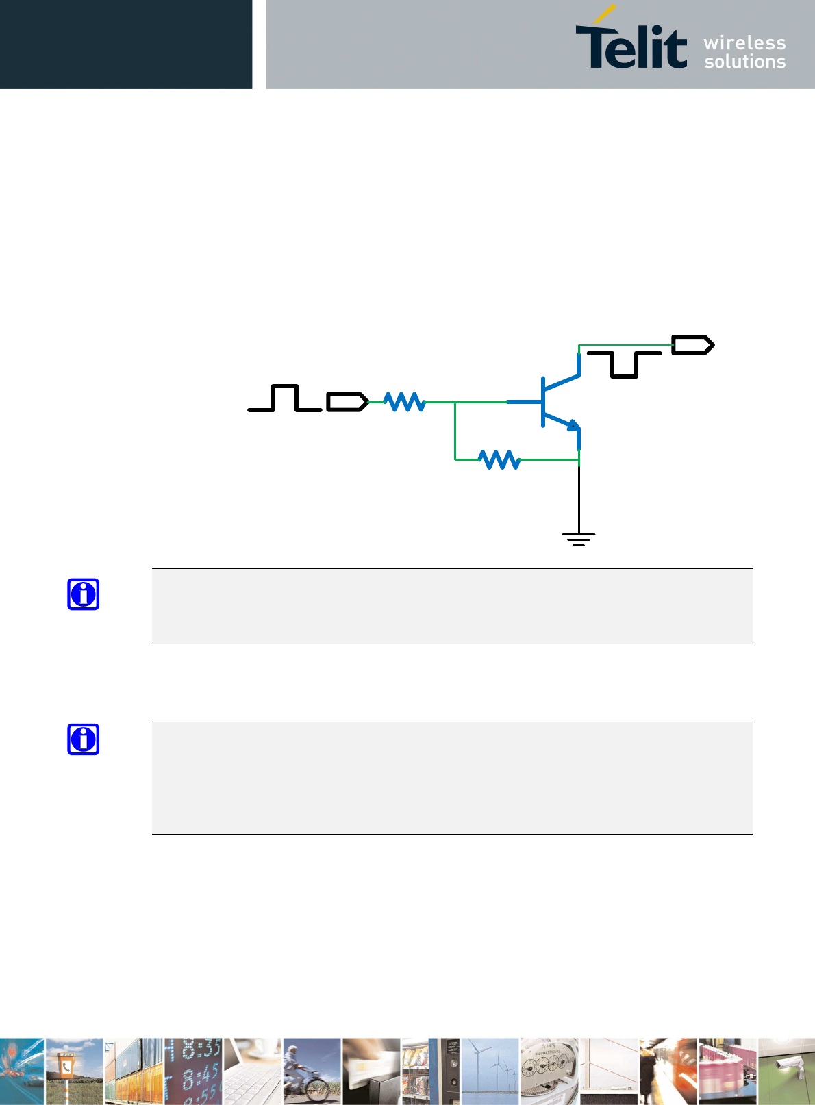
LE940B6 Hardware User Guide
1VV0301331 Rev. 1.8 - 2017-03-15
Reproduction forbidden without written authorization by Telit Communications S.p.A. - All Rights Reserved
Telit Confidential Information, provided under NDA Page
51 of 104
5.3.3. Unconditional Hardware Reset (RESET_N)
To unconditionally restart the LE940B6 module, the RESET_N pad must be tied low in the range
1300 - 1800 milliseconds and then released.
Figure 9 shows a simple circuit for this action.
Figure 9: Circuit for Unconditional Hardware Reset
GND
R1
R2
Q1
Unconditional
Reset Impulse
1300ms < Hold Time < 1800ms
RESET_N
NOTE:
The Unconditional Hardware Reset must always be implemented on the boards, but the software
must use it only as an emergency exit procedure, and not as a normal power-off operation.
NOTE:
Do not use any pull-up resistor on the RESET_N line or any totem pole digital output. Using a pull-
up resistor may cause latch-up problems on the LE940B6 power regulator and improper
functioning of the module. The RESET_N line must be connected only in an open-collector
configuration.
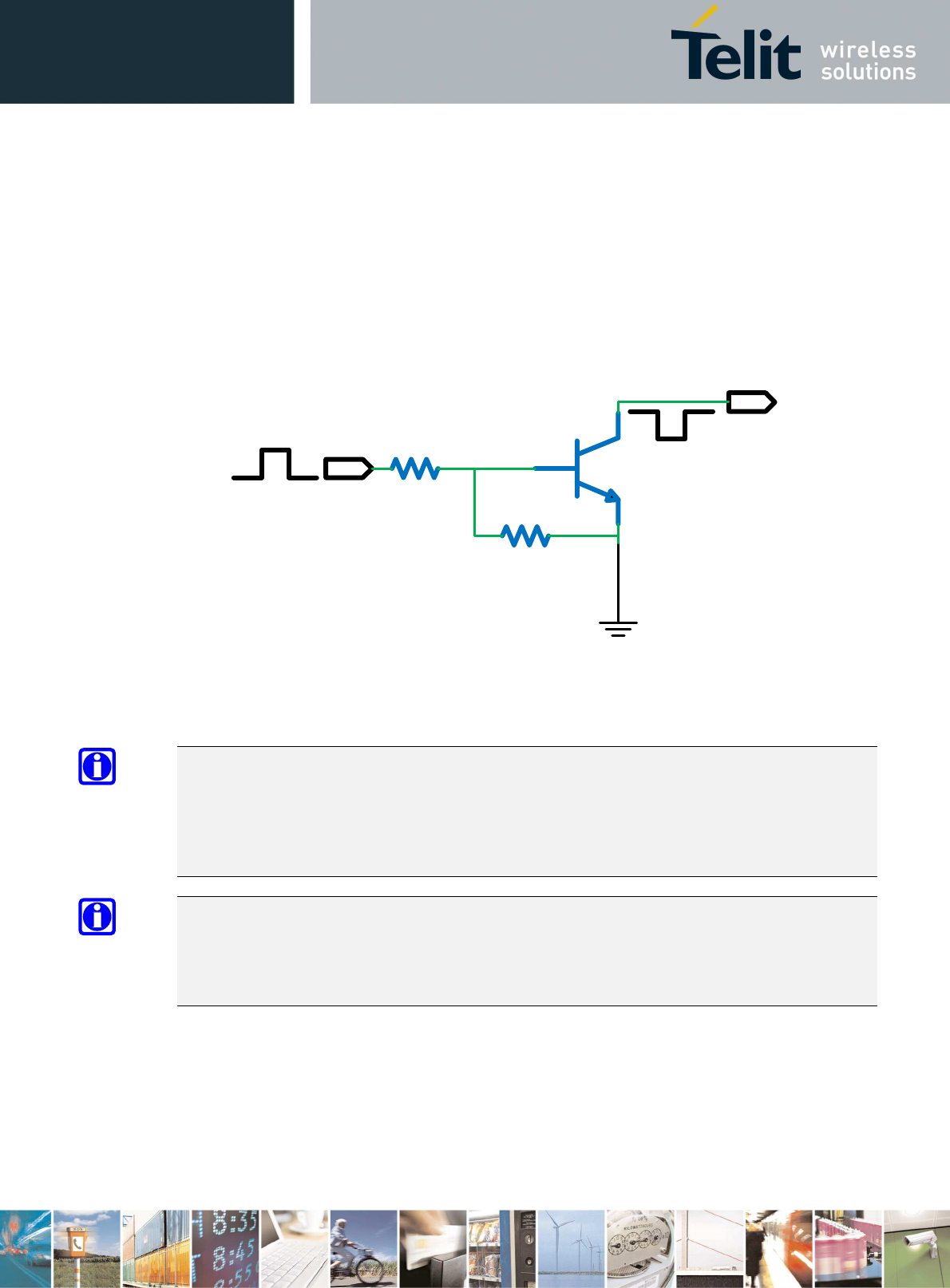
LE940B6 Hardware User Guide
1VV0301331 Rev. 1.8 - 2017-03-15
Reproduction forbidden without written authorization by Telit Communications S.p.A. - All Rights Reserved
Telit Confidential Information, provided under NDA Page
52 of 104
5.3.4. Unconditional Hardware Shutdown
To unconditionally shut down the LE940B6 module, the SHDN_N pad must be tied low for at least
200 milliseconds and then released.
Figure 10 shows a simple circuit for applying an unconditional shutdown.
Figure 10: Circuit for Unconditional Hardware Shutdown
GND
R1
R2
Q1
Unconditional
Shutdown Impulse
At least 200ms
SHDN_N
To check whether the device has powered off, monitor the VAUX/PWRMON hardware line. When
VAUX/PWRMON goes low, the device has powered off.
NOTE:
Do not use any pull-up resistor on the SHDN_N line or any totem pole digital output. Using a pull-
up resistor may cause latch-up problems on the LE940B6 power regulator and improper
functioning of the module. The SHDN_N line must be connected only in an open-collector
configuration.
NOTE:
The Unconditional Hardware Shutdown (SHDN_N) must always be implemented on the boards,
but the software must use it only as an emergency exit procedure, and not as a normal power-off
operation.
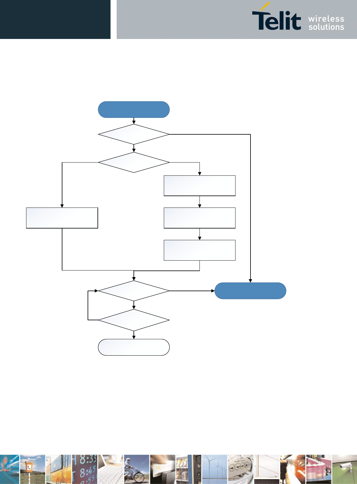
LE940B6 Hardware User Guide
1VV0301331 Rev. 1.8 - 2017-03-15
Reproduction forbidden without written authorization by Telit Communications S.p.A. - All Rights Reserved
Telit Confidential Information, provided under NDA Page
53 of 104
Figure 11 shows a flow chart of the proper turn off procedure.
Figure 11: Turn Off Procedure
Modem OFF Procedure
START
VAUX/PWRMON = ON?
OFF Mode
ON_OFF_N = LOW
Delay = 200 ms
ON_OFF_N = HIGH
AT#SHDN
VAUX/PWRMON = ON?
Looping for more
6 sec
Modem OFF Procedure
END
Go to
Start AT CMD
Y
HW SHUTDOWNSW SHUTDOWN
Y
Y
N
N
N

LE940B6 Hardware User Guide
1VV0301331 Rev. 1.8 - 2017-03-15
Reproduction forbidden without written authorization by Telit Communications S.p.A. - All Rights Reserved
Telit Confidential Information, provided under NDA Page
54 of 104
6. Power Supply
The power supply circuitry and board layout are very important parts of the full product design,
with critical impact on the overall product performance. Read the following requirements and
guidelines carefully to ensure a good and proper design.
6.1. Power Supply Requirements
The LE940B6 power requirements are as follows:
Table 20: Power Supply Requirements
Nominal supply voltage 3.8V
Supply voltage range 3.4V – 4.2V
Max ripple on module input supply 30 mV
Table 21 provides typical current consumption values of LE940B6 for the various available modes.
Table 21: LE940B6 Current Consumption
Mode Average (Typ.)
Mode Description
Switched Off
Switched off 0.1 mA Module supplied but switched Off
Idle Mode (Standby Mode; No Call in Progress)
AT+CFUN=4 2.5 mA Tx and Rx disabled ; module is not registered on the
network (Flight mode)
DRx
GSM 4.7 mA DRx5
WCDMA 4.7 mA DRx6
3.6 mA DRx7
3.1 mA DRx8
2.8 mA DRx9
LTE 7.7 mA Paging cycle #32 frames (0.32 sec DRx cycle)
5.1 mA Paging cycle #64 frames (0.64 sec DRx cycle)

LE940B6 Hardware User Guide
1VV0301331 Rev. 1.8 - 2017-03-15
Reproduction forbidden without written authorization by Telit Communications S.p.A. - All Rights Reserved
Telit Confidential Information, provided under NDA Page
55 of 104
Mode Average (Typ.)
Mode Description
3.8 mA Paging cycle #128 frames (1.28 sec DRx cycle)
3.2 mA Paging cycle #256 frames (2.56 sec DRx cycle)
Operative Mode (LTE)
LTE (0dBm)
300 mA LTE data call (Non-CA BW 5 MHz, RB=1)
500 mA LTE data call (CA BW 20 + 20MHz, Full RB, B4+B4 Intra
CA, FDD 300 Mbps DL / 50 Mbps UL) without Ethernet
750 mA LTE data call (CA BW 20 + 20MHz, Full RB, B4+B4 Intra
CA, FDD 300 Mbps DL / 50 Mbps UL) with Ethernet
LTE (23dBm)
760 mA LTE data call (Non-CA BW 5MHz, RB=1)
1000 mA LTE data call (CA BW 20 + 20MHz, Full RB, B4+B4 Intra
CA, FDD 300 Mbps DL / 50 Mbps UL) without Ethernet
1250 mA LTE data call (CA BW 20 + 20MHz, Full RB, B4+B4 Intra
CA, FDD 300 Mbps DL / 50 Mbps UL) with Ethernet
Operative Mode (WCDMA)
WCDMA Voice 690 mA WCDMA voice call (Tx = 23 dBm)
WCDMA HSDPA
(0 dBm)
300 mA WCDMA data call (DC-HSDPA up to 42 Mbps, Max
Throughput) without Ethernet
550 mA WCDMA data call (DC-HSDPA up to 42 Mbps, Max
Throughput) with Ethernet
WCDMA HSDPA
(23 dBm)
700 mA WCDMA data call (DC-HSDPA up to 42 Mbps, Max
Throughput) without Ethernet
950 mA WCDMA data call (DC-HSDPA up to 42 Mbps, Max
Throughput) with Ethernet
Operative Mode (GSM)
GSM Tx and Rx mode
GSM 850/900 PL5 360 mA GSM voice call
LE940B6 Hardware User Guide
1VV0301331 Rev. 1.8 - 2017-03-15
Reproduction forbidden without written authorization by Telit Communications S.p.A. - All Rights Reserved
Telit Confidential Information, provided under NDA Page
56 of 104
Mode Average (Typ.)
Mode Description
GSM 1800/1900
PL0
300 mA
GPRS 4 Tx + 1 Rx
GSM 850/900 PL5 750 mA
GPRS Sending Data mode (CS-4)
DCS 1800/1900 PL0
550 mA
EGPRS 4 Tx + 1 Rx
GSM 850/900 PL8 550 mA
GPRS Sending Data mode (MCS-5)
DCS 1800/1900 PL2
500 mA
* Worst/best case current values depend on network configuration, not under module control.
** Applied MPR –2dB 16-QAM full RB
*** 3.8V voltage/room temperature
NOTE:
Differences in measurement technique, equipment, or temperature can cause variations in
current consumption measurements.
NOTE:
The electrical design for the power supply must ensure a peak current output of at least 2.0A.
NOTE:
In GSM/GPRS mode, RF transmission is not continuous, but is packed into bursts at a base
frequency of about 216 Hz with relative current peaks as high as about 2.0A. Therefore, the
power supply must be designed to withstand these current peaks without big voltage drops. This
means that both the electrical design and the board layout must be designed for this current
flow.
If the layout of the PCB is not well designed, a strong noise floor is generated on the ground. This
will reflect on all the audio paths producing an audible annoying noise at 216 Hz.
If the voltage drops during the peaks, current absorption is too high. The device may even shut
down as a consequence of the supply voltage drop.

LE940B6 Hardware User Guide
1VV0301331 Rev. 1.8 - 2017-03-15
Reproduction forbidden without written authorization by Telit Communications S.p.A. - All Rights Reserved
Telit Confidential Information, provided under NDA Page
57 of 104
6.2. General Design Rules
The principal guidelines for the Power Supply Design embrace three different design steps:
• Electrical design
• Thermal design
• PCB layout
6.2.1. Electrical Design Guidelines
The electrical design of the power supply depends strongly on the power source where this
power is drained. Power sources can be distinguished by three categories:
• +5V input (typically PC internal regulator output)
• +12V input (typically automotive)
• Battery
6.2.1.1. + 5V Input Source Power Supply – Design Guidelines
• The desired output for the power supply is 3.8V. So, the difference between the input source
and the desired output is not big, and therefore a linear regulator can be used. A switching
power supply is preferred to reduce power consumption.
• When using a linear regulator, a proper heat sink must be provided to dissipate the power
generated.
• A bypass low ESR capacitor of adequate capacity must be provided to cut the current
absorption peaks close to the LE940B6 module. A 100 μF tantalum capacitor is usually
suitable on both VBATT and VBATT_PA power lines.
• Make sure that the low ESR capacitor on the power supply output (usually a tantalum one) is
rated at least 10V.
• A protection diode must be inserted close to the power input to protect the LE940B6 module
from power polarity inversion.
Figure 12 shows an example of linear regulator with 5V input.
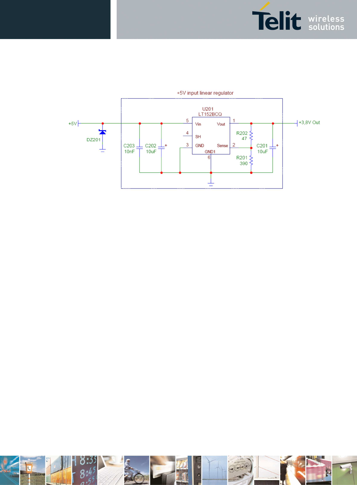
LE940B6 Hardware User Guide
1VV0301331 Rev. 1.8 - 2017-03-15
Reproduction forbidden without written authorization by Telit Communications S.p.A. - All Rights Reserved
Telit Confidential Information, provided under NDA Page
58 of 104
Figure 12: Example of Linear Regulator with 5V Input
6.2.1.2. + 12V Input Source Power Supply – Design Guidelines
• The desired output for the power supply is 3.8V. Due to the big difference between the input
source and the desired output, a linear regulator is unsuitable and must not be used. A
switching power supply is preferable because of its better efficiency, especially with the
2A peak current load expected when working with the LE940B6.
• When using a switching regulator, a 500-kHz or higher switching frequency regulator is
preferable because of its smaller inductor size and its faster transient response. This allows
the regulator to respond quickly to the current peaks absorption.
• In any case, the selection of the frequency and switching design is related to the application
to be developed due to the fact that the switching frequency can also generate EMC
interference.
• For car batteries (lead-acid accumulators) the input voltage can rise up to 15.8V. This must be
kept in mind when choosing components: all components in the power supply must
withstand this voltage.
• A bypass low ESR capacitor of adequate capacity must be provided to cut the current
absorption peaks. A 100μF tantalum capacitor is usually suitable on VBATT & VBATT_PA
power lines.
• Make sure that the low ESR capacitor on the power supply output (usually a tantalum one) is
rated at least 10V.
• For automotive applications, a spike protection diode must be inserted close to the power
input to clean the supply of spikes.
• A protection diode must be inserted close to the power input to protect the LE940B6 module
from power polarity inversion. This can be the same diode as for spike protection.
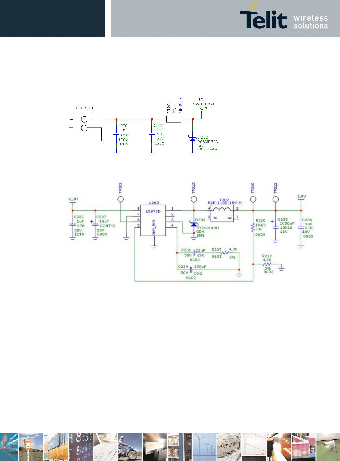
LE940B6 Hardware User Guide
1VV0301331 Rev. 1.8 - 2017-03-15
Reproduction forbidden without written authorization by Telit Communications S.p.A. - All Rights Reserved
Telit Confidential Information, provided under NDA Page
59 of 104
Figure 13 and Figure 14 show an example of switching regulator with 12V input.
Figure 13: Example of Switching Regulator with 12V Input – Part 1
Figure 14: Example of Switching Regulator with 12V Input – Part 2

LE940B6 Hardware User Guide
1VV0301331 Rev. 1.8 - 2017-03-15
Reproduction forbidden without written authorization by Telit Communications S.p.A. - All Rights Reserved
Telit Confidential Information, provided under NDA Page
60 of 104
6.2.1.3. Battery Source Power Supply – Design Guidelines
• The desired nominal output for the power supply is 3.8V, and the maximum allowed voltage
is 4.2V. Hence, a single 3.7V Li-Ion cell battery type is suitable for supplying the power to the
LE940B6 module.
NOTE:
Do not use any Ni-Cd, Ni-MH, and Pb battery types directly connected to the LE940B6 module.
Their use can lead to overvoltage on the LE940B6 and damage it. Use only Li-Ion battery types.
• A bypass low ESR capacitor of adequate capacity must be provided to cut the current
absorption peaks; a 100μF tantalum capacitor is usually suitable.
• Make sure that the low ESR capacitor (usually a tantalum one) is rated at least 10V.
• A protection diode must be inserted close to the power input to protect the LE940B6 module
from power polarity inversion. Otherwise, the battery connector must be done in a way to
avoid polarity inversions when connecting the battery.
• The battery capacity must be at least 500 mAh to withstand the current peaks of 2A. The
suggested capacity is from 500 mAh to 1000 mAh.
LE940B6 Hardware User Guide
1VV0301331 Rev. 1.8 - 2017-03-15
Reproduction forbidden without written authorization by Telit Communications S.p.A. - All Rights Reserved
Telit Confidential Information, provided under NDA Page
61 of 104
6.2.2. Thermal Design Guidelines
The thermal design for the power supply heat sink must be done with the following specifications:
• Average current consumption during LTE 2xCA DL Max throughput @PWR level max in
LE940B6: 1250 mA
NOTE:
The average consumption during transmission depends on the power level at which the device is
requested to transmit via the network. Therefore, the average current consumption varies
significantly.
In LTE mode, the LE940B6 emits RF signals continuously during transmission. Therefore, pay
special attention to how the generated heat is dissipated.
The current consumption is up to about 1250 mA in 2xCA Max throughput, and 1250 mA in LTE
continuously at the maximum Tx output power 23.0 dBm.
The current consumption is up to about 1250 mA continuously at the maximum Tx output power
(23 dBm). Therefore, make sure on the PCB used to mount LE940B6, that the area under the
LE940B6 module is as large as possible. Make sure that the LE940B6 is mounted on the large
ground area of application board and provide many ground vias to dissipate the heat.
6.2.3. Power Supply PCB Layout Guidelines
As seen in the electrical design guidelines, the power supply must have a low ESR capacitor on the
output to cut the current peaks and a protection diode on the input to protect the supply from
spikes and polarity inversion. The placement of these components is crucial for the correct
operation of the circuitry. A misplaced component can be useless or can even decrease the power
supply performances.
• The bypass low ESR capacitor must be placed close to the LE940B6 power input pads, or if the
power supply is of a switching type, it can be placed close to the inductor to cut the ripple, as
long as the PCB trace from the capacitor to LE940B6 is wide enough to ensure a drop-less
connection even during the 2A current peaks.
• The protection diode must be placed close to the input connector where the power source is
drained.
• The PCB traces from the input connector to the power regulator IC must be wide enough to
ensure that no voltage drops occur during the 2A current peaks.
Note that this is not done to save power loss but especially to avoid the voltage drops on the
power line at the current peaks frequency of 216 Hz that will reflect on all the components
connected to that supply (also introducing the noise floor at the burst base frequency.)
For this reason while a voltage drop of 300-400 mV may be acceptable from the power loss
point of view, the same voltage drop may not be acceptable from the noise point of view. If
your application does not have an audio interface but only uses the data feature of the
LE940B6, this noise is not so disturbing, and the power supply layout design can be more
forgiving.

LE940B6 Hardware User Guide
1VV0301331 Rev. 1.8 - 2017-03-15
Reproduction forbidden without written authorization by Telit Communications S.p.A. - All Rights Reserved
Telit Confidential Information, provided under NDA Page
62 of 104
• The PCB traces to LE940B6 and the bypass capacitor must be wide enough to ensure that no
significant voltage drops occur when the 2A current peaks are absorbed. This is needed for
the same above-mentioned reasons. Try to keep these traces as short as possible.
• The PCB traces connecting the switching output to the inductor and the switching diode must
be kept as short as possible by placing the inductor and the diode very close to the power
switching IC (only for the switching power supply). This is done to reduce the radiated field
(noise) at the switching frequency (usually 100-500 kHz).
• Use a good common ground plane.
• Place the power supply on the board in a way to guarantee that the high current return paths
in the ground plane do not overlap any noise sensitive circuitry, such as the microphone
amplifier/buffer or earphone amplifier.
• The power supply input cables must be kept separate from noise sensitive lines, such as
microphone/earphone cables.
LE940B6 Hardware User Guide
1VV0301331 Rev. 1.8 - 2017-03-15
Reproduction forbidden without written authorization by Telit Communications S.p.A. - All Rights Reserved
Telit Confidential Information, provided under NDA Page
63 of 104
7. Antenna(s)
Antenna connection and board layout design are the most important parts in the full product
design, and they have a strong influence on the product’s overall performance. Read carefully and
follow the requirements and guidelines for a good and proper design.
7.1. GSM/WCDMA/TD-SCDMA/LTE Antenna Requirements
The antenna for the LE940B6 device must meet the following requirements:
Table 22: Primary Antenna Requirements
Gain Gain < 3 dBi
Impedance 50 Ohm
Input power > 33 dBm(2 W) peak power in GSM
> 24 dBm average power in WCDMA & LTE
VSWR absolute max <= 10:1
VSWR recommended <= 2:1
The antenna for a specific car model must support a given set of RF bands. This set is determined
by the region variant and the specific set of bands within (either the full band set offered by Telit
or a subset per the customer choice). The antenna must have the proper bandwidth to support
the required set of bands and meet the other performance figures according to the Table 22,
along the full bandwidth. The RF bands supported in each region variant are detailed in
Section 2.5.1, RF Bands per Regional Variant.
Since there is no antenna connector on the LE940B6 module, the antenna must be connected to
the LE940B6 antenna pad (AD1) by a transmission line implemented on the PCB.
If the antenna is not directly connected to the antenna pad of the LE940B6, a PCB line is required
to connect to it or to its connector.
7.2. GSM/WCDMA/TD-SCDMA/LTE Antenna – PCB Line Guidelines
• Make sure that the transmission line’s characteristic impedance is 50 Ohm.
• Keep the line on the PCB as short as possible since the antenna line loss should be less than
around 0.3 dB.
• Line geometry should have uniform characteristics, constant cross sections, and avoid
meanders and abrupt curves.
• Any suitable geometry/structure can be used for implementing the printed transmission line
affecting the antenna.
LE940B6 Hardware User Guide
1VV0301331 Rev. 1.8 - 2017-03-15
Reproduction forbidden without written authorization by Telit Communications S.p.A. - All Rights Reserved
Telit Confidential Information, provided under NDA Page
64 of 104
• If a ground plane is required in the line geometry, this plane must be continuous and
sufficiently extended so the geometry can be as similar as possible to the related canonical
model.
• Keep, if possible, at least one layer of the PCB used only for the ground plane. If possible, use
this layer as reference ground plane for the transmission line.
• Surround the PCB transmission line with ground (on both sides). Avoid having other signal
tracks facing the antenna line track directly.
• Avoid crossing any un-shielded transmission line footprint with other tracks on different
layers.
• The ground surrounding the antenna line on the PCB must be strictly connected to the main
Ground plane by means of via-holes (once per 2 mm at least) placed close to the ground
edges facing the line track.
• Place EM-noisy devices as far as possible from LE940B6 antenna line.
• Keep the antenna line far away from the LE940B6 power supply lines.
• If EM-noisy devices are present on the PCB hosting the LE940B6, such as fast switching ICs,
take care to shield them with a metal frame cover.
• If EM-noisy devices are not present around the line, geometries like Micro strip or Grounded
Coplanar Waveguide are preferred because they typically ensure less attenuation compared
to a Strip line having the same length.
This transmission line must meet the following requirements:
Table 23: Antenna Line on PCB Requirements
Characteristic impedance 50 Ohm
Max attenuation 0.3 dB
Avoid coupling with other signals.
Cold End (Ground Plane) of the antenna must be equipotential to the LE940B6 ground pads.
Furthermore if the device is developed for the US and/or Canada market, it must comply with the
FCC and/or IC approval requirements:
This device is to be used only for mobile and fixed application. The antenna(s) used for this
transmitter must be installed to provide a separation distance of at least 20 cm from all persons
and must not be co-located or operating in conjunction with any other antenna or transmitter. End-
Users must be provided with transmitter operation conditions for satisfying RF exposure compliance.
OEM integrators must ensure that the end user has no manual instructions to remove or install the
LE940B6 module. Antennas used for this OEM module must not exceed 3dBi gain for mobile and
fixed operating configurations.
LE940B6 Hardware User Guide
1VV0301331 Rev. 1.8 - 2017-03-15
Reproduction forbidden without written authorization by Telit Communications S.p.A. - All Rights Reserved
Telit Confidential Information, provided under NDA Page
65 of 104
7.3. GSM/WCDMA/TD-SCDMA/LTE Antenna – Installation Guidelines
• Install the antenna in a location with access to the network radio signal.
• The antenna must be installed such that it provides a separation distance of at least 20 cm
from all persons and must not be co-located or operating in conjunction with any other
antenna or transmitter.
• The antenna must not be installed inside metal cases.
• The antenna must be installed according to the antenna manufacturer’s instructions.
7.4. Secondary Antenna Requirements
This product includes an input for a second Rx antenna to improve radio sensitivity. The function
is called Antenna Diversity.
Since there is no antenna connector on the LE940B6 module, the antenna must be connected to
the LE940B6 antenna pad by means of a transmission line implemented on the PCB.
If the antenna is not directly connected at the antenna pad of the LE940B6 (AU9), a PCB line is
required to connect to it or to its connector.
The second Rx antenna must not be located in close vicinity of the main antenna. To improve
diversity gain and isolation and to reduce mutual interaction, the two antennas should be located
at the maximum reciprocal distance possible, taking into consideration the available space within
the application.
NOTE:
If Rx Diversity is not used/connected, disable the Diversity functionality using the AT+XRXDIV
command (refer to Ref 1: LE940B6 AT Command Reference Guide) and connect the Diversity pad
AU9 to a 50 Ohm termination.
7.5. PCB Guidelines in case of FCC certification
In the case FCC certification is required for an application using LE940B6-NA, according to FCC
KDB 996369 for modular approval requirements, the transmission line has to be similar to that
implemented on module’s interface board and described in the following chapter.
7.5.1. Transmission line design
During the design of the interface board, the placement of components has been chosen
properly, in order to keep the line length as short as possible, thus leading to lowest power losses
possible. A Grounded Coplanar Waveguide (G-CPW) line has been chosen, since this kind of
transmission line ensures good impedance control and can be implemented in an outer PCB layer
as needed in this case. A SMA female connector has been used to feed the line.
LE940B6 Hardware User Guide
1VV0301331 Rev. 1.8 - 2017-03-15
Reproduction forbidden without written authorization by Telit Communications S.p.A. - All Rights Reserved
Telit Confidential Information, provided under NDA Page
66 of 104
The interface board is realized on a FR4, 4-layers PCB. Substrate material is characterized by
relative permittivity εr = 4.6 ± 0.4 @ 1 GHz, TanD= 0.019 ÷ 0.026 @ 1 GHz.
A characteristic impedance of nearly 50 Ω is achieved using trace width = 1.1 mm, clearance from
coplanar ground plane = 0.3 mm each side. The line uses reference ground plane on layer 3, while
copper is removed from layer 2 underneath the line. Height of trace above ground plane is 1.335
mm. Calculated characteristic impedance is 51.6 Ω, estimated line loss is less than 0.1 dB. The line
geometry is shown below:
7.5.2. Transmission line measurements
E5071C NA (Full-4-port calibration) has been used in this measurement session. A calibrated
coaxial cable has been soldered at the pad corresponding to RF output; a SMA connector has
been soldered to the board in order to characterize the losses of the transmission line including
the connector itself. During Return Loss / impedance measurements, the transmission line has
been terminated to 50 Ω load.
Return Loss plot of line under test is shown below:
LE940B6 Hardware User Guide
1VV0301331 Rev. 1.8 - 2017-03-15
Reproduction forbidden without written authorization by Telit Communications S.p.A. - All Rights Reserved
Telit Confidential Information, provided under NDA Page
67 of 104
Line input impedance (in Smith Chart format, once the line has been terminated to 50 Ω load) is
shown in the following figure:
LE940B6 Hardware User Guide
1VV0301331 Rev. 1.8 - 2017-03-15
Reproduction forbidden without written authorization by Telit Communications S.p.A. - All Rights Reserved
Telit Confidential Information, provided under NDA Page
68 of 104
Insertion Loss of G-CPW line plus SMA connector is shown below:
LE940B6 Hardware User Guide
1VV0301331 Rev. 1.8 - 2017-03-15
Reproduction forbidden without written authorization by Telit Communications S.p.A. - All Rights Reserved
Telit Confidential Information, provided under NDA Page
69 of 104
8. Hardware Interfaces
Table 24 summarizes all the hardware interfaces of the LE940B6 module.
Table 24: LE940B6 Hardware Interfaces
LE940B6 (XMM7272 CAT6)
Ethernet RMII/RGMII
USB USB2.0
SPI Master only, up to 26 MHz (104 MHz @ Kernel CLK/4)
I2C For sensors, audio control
UART x1 UART for AT (up to 4.8 Mbps)
x1 UART for diagnosis (up to 4.8 Mbps)
x1 UART for GNSS or external controller (up to 4.8 Mbps)
Audio I/F I2S/PCM, Analog audio
GPIO 15 dedicated GPIO
USIM X2, dual voltage each (1.8/2.9V);
SIM chip integration not possible
ADC Up to x3
Antenna ports 2 for Cellular, 1 for GNSS
LE940B6 Hardware User Guide
1VV0301331 Rev. 1.8 - 2017-03-15
Reproduction forbidden without written authorization by Telit Communications S.p.A. - All Rights Reserved
Telit Confidential Information, provided under NDA Page
70 of 104
8.1. USB Port
The LE940B6 module includes a Universal Serial Bus (USB) transceiver, which operates at USB
high-speed (480Mbits/sec). It can also operate with USB full-speed hosts (12Mbits/sec).
It is compliant with the USB 2.0 specification and can be used for control and data transfers as
well as for diagnostic monitoring and firmware update.
NOTE:
With the LE940B6 module, firmware updates by the host are only possible via USB and not
possible via UART. The reason is that Telit considers it impractical to transfer firmware binaries
exceeding 100Mb via UART.
The USB port is typically the main interface between the LE940B6 module and OEM hardware.
NOTE:
The USB_D+ and USB_D- signals have a clock rate of 480 MHz. The signal traces must be routed
carefully. Minimize trace lengths, number of vias, and capacitive loading. The impedance value
should be as close as possible to 90 Ohms differential.
The pull-up, pull-down and series resistors on pins USB_D+ and USB_D- as required by the USB
2.0 specification are included inside the module.
Table 25 lists the USB interface signals.
Table 25: USB Interface Signals
Signal Pad
No.
Usage
USB_VBUS A18 Power and cable detection for the internal USB transceiver.
Acceptable input voltage range 2.5V – 5.5V @ max 5 mA consumption
USB_D- F19 Minus (-) line of the differential, bi-directional USB signal to/from the
peripheral device
USB_D+ D19 Plus (+) line of the differential, bi-directional USB signal to/from the
peripheral device
NOTE:
USB_VBUS input power is internally used to detect the USB port and start the enumeration
process. It is not used for supplying power to the internal LE940B6 USB HW block.
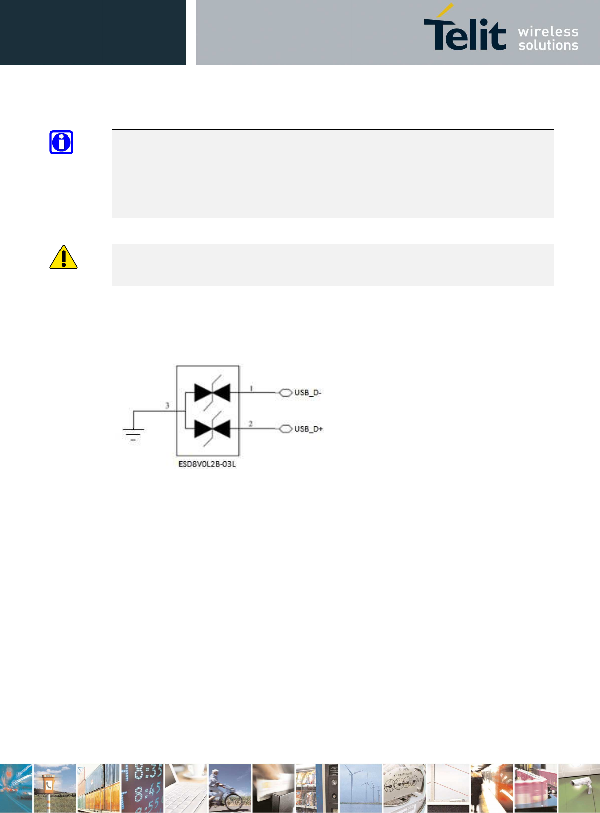
LE940B6 Hardware User Guide
1VV0301331 Rev. 1.8 - 2017-03-15
Reproduction forbidden without written authorization by Telit Communications S.p.A. - All Rights Reserved
Telit Confidential Information, provided under NDA Page
71 of 104
NOTE:
Even if USB communication is not used, it is still highly recommended to place an optional USB
connector on the application board.
At least test points of the USB signals are required since the USB physical communication is
needed in the case of SW update.
Warning:
Consider placing low-capacitance ESD protection device to protect LE940B6 against ESD strikes.
If an ESD protection should be added, the suggested connectivity is as follows:
Figure 15: ESD Protection for USB2.0
8.2. Serial Ports
The serial port is typically a secondary interface between the LE940B6 module and OEM
hardware. The following serial ports are available on the module:
• Modem Serial Port 1 (Main)
• Modem Serial Port 2 (Auxiliary)
• Modem Serial Port 3 (GNSS)
Several serial port configurations can be designed for the OEM hardware. The most common are:
• RS232 PC com port
• Microcontroller UART @ 1.8V (Universal Asynchronous Receive Transmit)
• Microcontroller UART @ 3.3V/5V or other voltages different from 1.8V
Depending on the type of serial port on OEM hardware, level translator circuits may be needed to
make the system operate. The only configuration that does not need level translation is the 1.8V
UART. The LE940B6 UART has CMOS levels as described in Section 4.3.1, 1.8V Standard GPIOs.
LE940B6 Hardware User Guide
1VV0301331 Rev. 1.8 - 2017-03-15
Reproduction forbidden without written authorization by Telit Communications S.p.A. - All Rights Reserved
Telit Confidential Information, provided under NDA Page
72 of 104
8.2.1. Modem Serial Port 1
Serial Port 1 is a +1.8V UART, having all the 8 RS232 signals. It differs from the PC-RS232 in the
signal polarity (RS232 is reversed) and levels. Table 26 lists the signals of LE940B6 Serial Port 1.
Table 26: Modem Serial Port 1 Signals
RS232 Pin #
Signal Pad No.
Name Usage
1 DCD -
DCD_UART
AE18 Data Carrier
Detect
Output from LE940B6 that
indicates carrier presence
2 RXD -
TX_UART
AF19 Transmit line
*see Note
Output transmit line of LE940B6
UART
3 TXD -
RX_UART
AH19 Receive line
*see Note
Input receive line of LE940B6 UART
4 DTR -
DTR_UART
AC18 Data Terminal
Ready
Input to LE940B6 that controls the
DTE READY condition
5 DSR -
DSR_UART
AG18 Data Set Ready Output from LE940B6 that
indicates that the module is ready
6 RTS -
RTS_UART
AA18 Request to Send
Input to LE940B6 controlling the
Hardware flow control
7 CTS -
CTS_UART
AK19 Clear to Send Output from LE940B6 controlling
the Hardware flow control
8 RI -
RI_UART
AJ18 Ring Indicator Output from LE940B6 indicating
the Incoming call condition
NOTE:
To avoid a back-powering effect, it is recommended to avoid having any HIGH logic level signal
applied to the digital pins of the module when it is powered OFF or during an ON/OFF transition.
NOTE:
For minimum implementations, only the TXD and RXD lines need be connected. The other lines
can be left open provided a software flow control is implemented.
NOTE:
According to V.24, Rx/Tx signal names refer to the application side; therefore, on the LE940B6
side, these signal are in the opposite direction: TXD on the application side will be connected to
the receive line (here named TXD/ RX_UART) of the LE940B6 serial port and vice versa for Rx.
LE940B6 Hardware User Guide
1VV0301331 Rev. 1.8 - 2017-03-15
Reproduction forbidden without written authorization by Telit Communications S.p.A. - All Rights Reserved
Telit Confidential Information, provided under NDA Page
73 of 104
8.2.2. Modem Serial Port 2
On the LE940B6, Serial Port 2 is a +1.8V UART with Rx and Tx signals only.
Table 27 lists the signals of the LE940B6 Serial Port 2.
Table 27: Modem Serial Port 2 Signals
PAD Signal I/O
Function Type
COMMENT
AB19 TXD_AUX O Auxiliary UART (Tx Data to DTE) 1.8V
AD19 RXD_AUX I Auxiliary UART (Rx Data to DTE) 1.8V
NOTE:
To avoid a back-powering effect, it is recommended to avoid having any HIGH logic level signal
applied to the digital pins of the module when it is powered OFF or during an ON/OFF transition.
NOTE:
The Auxiliary UART is used as the SW main debug console. It is required to place test points on
this interface even if not used.
8.2.3. Modem Serial Port 3
Serial port 3 is a +1.8V UART with all 4 RS232 signals. It differs from the PC-RS232 in the signal
polarity (RS232 is reversed) and levels. Table 28 lists the signals of the LE940B6 Serial Port 3.
Table 28: Modem Serial Port 3 Signals
PAD Signal I/O
Function Type
Comment
AM9 UART3_TXD
I Serial data input (TXD) from DTE 1.8V
AM11
UART3_RXD
O Serial data output (RXD) to DTE 1.8V
AM13
UART3_RTS
I Input for Request to Send (RTS) from DTE
1.8V
AM15
UART3_CTS
O Output for Clear to Send (CTS) to DTE 1.8V
NOTE:
To avoid a back-powering effect, it is recommended to avoid having any HIGH logic level signal
applied to the digital pins of the module when it is powered OFF or during an ON/OFF transition.
LE940B6 Hardware User Guide
1VV0301331 Rev. 1.8 - 2017-03-15
Reproduction forbidden without written authorization by Telit Communications S.p.A. - All Rights Reserved
Telit Confidential Information, provided under NDA Page
74 of 104
8.2.4. RS232 Level Translation
To interface the LE940B6 with a PC COM port or an RS232 (EIA/TIA-232) application, a level
translator is required. This level translator must perform the following actions:
• Invert the electrical signal in both directions
• Change the level from 0/1.8V to +15/-15V
The RS232 UART 16450, 16550, 16650 & 16750 chipsets accept signals with lower levels on the
RS232 side (EIA/TIA-562), allowing a lower voltage-multiplying ratio on the level translator. Note
that the negative signal voltage must be less than 0V and hence some sort of level translation is
always required.
The simplest way to translate the levels and invert the signal is by using a single chip-level
translator. There are a multitude of them, differing in the number of drivers and receivers and in
the levels (be sure to get a true RS232 level translator, not a RS485 or other standards).
By convention, the driver is the level translator from the 0-1.8V UART to the RS232 level. The
receiver is the translator from the RS232 level to 0-1.8V UART. To translate the whole set of
control lines of the UART, the following is required:
• 2 drivers
• 2 receivers
Warning:
The digital input lines, operating at 1.8V CMOS levels, have absolute maximum input voltage of
2.0V. The level translator IC outputs on the module side (i.e. LE940B6 inputs) will cause
damage to the module inputs if the level translator is powered with +3.8V power.
So the level translator IC must be powered from a dedicated +1.8V power supply.
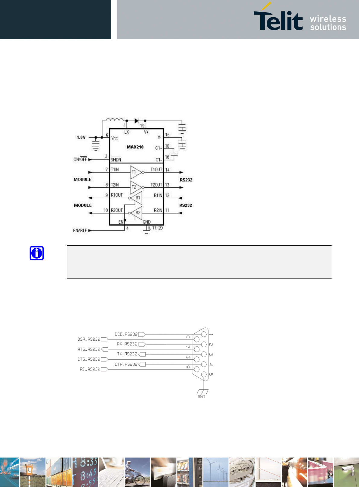
LE940B6 Hardware User Guide
1VV0301331 Rev. 1.8 - 2017-03-15
Reproduction forbidden without written authorization by Telit Communications S.p.A. - All Rights Reserved
Telit Confidential Information, provided under NDA Page
75 of 104
As an example of RS232 level adaption circuitry could use a MAXIM transceiver (MAX218). In this
case, the chipset is capable of translating directly from 1.8V to the RS232 levels (Example on 4
signals only).
Figure 16: RS232 Level Adaption Circuitry Example
NOTE:
In this case, the length of the lines on the application must be taken into account to avoid
problems in the case of High-speed rates on RS232.
The RS232 serial port lines are usually connected to a DB9 connector as shown in Figure 17. Signal
names and directions are named and defined from the DTE point of view.
Figure 17: RS232 Serial Port Lines Connection Layout

LE940B6 Hardware User Guide
1VV0301331 Rev. 1.8 - 2017-03-15
Reproduction forbidden without written authorization by Telit Communications S.p.A. - All Rights Reserved
Telit Confidential Information, provided under NDA Page
76 of 104
8.3. Peripheral Ports
In addition to the LE940B6 serial ports, the LE940B6 supports the following peripheral ports:
• SPI – Serial Peripheral Interface
• I2C - Inter-integrated circuit
• Ethernet – Ethernet PHY Interface
8.3.1. SPI – Serial Peripheral Interface
The LE940B6 SPI supports the following:
• Master Mode only
• 1.8V CMOS level
• Up to 26 MHz clock rate
NOTE:
SPI is supported only on the Linux side.
The LE940B6 module supports Master mode only and cannot be configured as Slave mode.
Table 29: SPI Signals
PAD Signal I/O Function Type Comment
P19 SPI_CLK O SPI clock output 1.8V
M19 SPI_MISO
I SPI data Master input Slave output 1.8V
K19 SPI_MOSI
O SPI data Master output Slave input 1.8V
N18 SPI_CS O SPI chip-select output 1.8V
Figure 18: SPI Signal Connectivity
LE940B6 (Master)
SPI_CS
SPI_CLK
SPI_MOSI
SPI_MISO
Host (Slave)
SPI_CS
SPI_CLK
SPI_MOSI
SPI_MISO
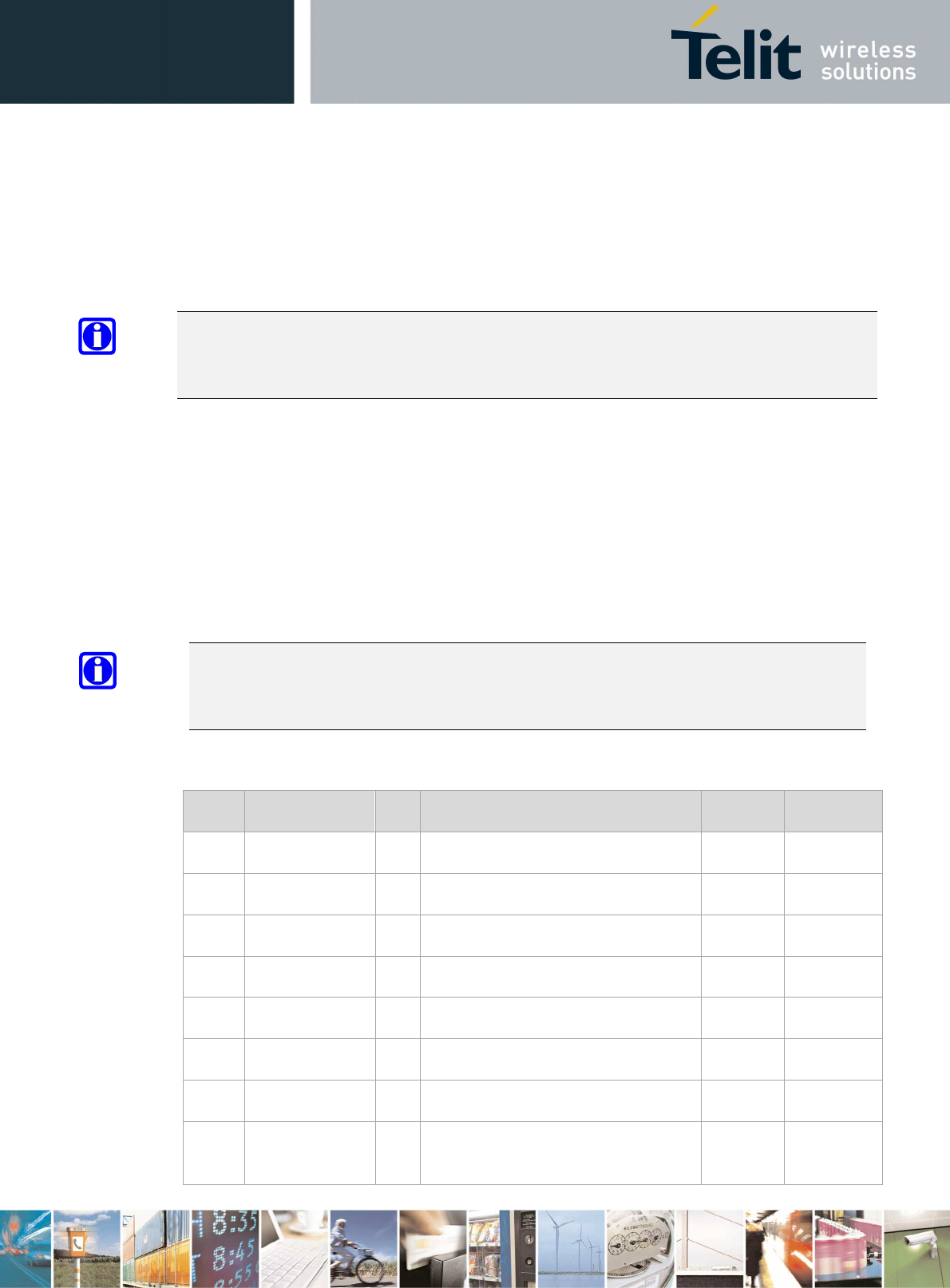
LE940B6 Hardware User Guide
1VV0301331 Rev. 1.8 - 2017-03-15
Reproduction forbidden without written authorization by Telit Communications S.p.A. - All Rights Reserved
Telit Confidential Information, provided under NDA Page
77 of 104
8.3.2. I2C - Inter-integrated Circuit
The LE940B6 I2C is an alternate function of GPIO 1-15 pins. Available only from Modem side as
SW emulation of I2C on GPIO lines. Any GPIO can be configured as SCL or SDA. LE940B6 supports
I2C Master Mode only.
NOTE:
SW emulated I2C on GPIO lines is supported only from the modem side. For more information,
refer to Ref 1: LE940B6 AT Command Reference Guide for command settings.
8.4. Ethernet Interface
The LE940B6 has an integrated Ethernet interface to an external Ethernet PHY supporting 10M /
100M and 1G speed modes via a RGMII interface.
The Ethernet interface is target to be compliant with the RGMII and RMII specifications. The
supported RGMII and RMII specification versions are:
• RGMII: Version 1.3, dated 12/10/2000, supporting up to 1000 Mbps operation
• RMII: Version 1.2, dated 03/20/1998, supporting up to 100 Mbps operation
NOTE:
Customer should carefully design the Ethernet interface depending on PHY chipset; Please
contact Telit R&D for more details and guidelines.
Table 30: Ethernet Interface
PAD Signal I/O
Function Type COMMENT
G14 MAC_MDC O Management Data Clock 2.5/3.3V
G12 MAC_MDIO I/O
Management Data I/O 2.5/3.3V
V16 MAC_TXD[0] O RGMII or RMII TXD[0] 2.5/3.3V
T16 MAC_TXD[1] O RGMII or RMII TXD[1] 2.5/3.3V
R16 MAC_TXD[2] O RGMII TXD[2] 2.5/3.3V
N16 MAC_TXD[3] O RGMII TXD[3] 2.5/3.3V
L16 MAC_GTX_CLK O RGMII Transmit Clock 2.5/3.3V
G16 MAC_TXEN_ER
O RGMII Transmit Enable /Error or
RMII Transmit Enable
2.5/3.3V

LE940B6 Hardware User Guide
1VV0301331 Rev. 1.8 - 2017-03-15
Reproduction forbidden without written authorization by Telit Communications S.p.A. - All Rights Reserved
Telit Confidential Information, provided under NDA Page
78 of 104
PAD Signal I/O
Function Type COMMENT
AL16 MAC_RXD[0] I RGMII or RMII RXD[0] 2.5/3.3V
AJ16 MAC_RXD[1] I RGMII or RMII RXD[1] 2.5/3.3V
AG16
MAC_RXD[2] I RGMII RXD[2] 2.5/3.3V
AE16 MAC_RXD[3] I RGMII RXD[3] 2.5/3.3V
AC16 MAC_RX_CLK I RGMII Receive Clock 2.5/3.3V
X16 MAC_RXDV_ER
I RGMII Receive Data Available/Error
or RMII Receive Error
2.5/3.3V
G10 ETH_INT_N I Ethernet PHY Interrupt 2.5/3.3V
G8 ETH_RST_N O Ethernet PHY Reset Output 2.5/3.3V
8.5. Audio Interface
The LE940B6 module supports analog and digital audio interfaces.
8.5.1. Analog Audio
The LE940B6 module provides an analog audio interface; a single differential input for the audio
to be transmitted (Uplink), and a balanced output for the received audio (Downlink). The analog
interface is on the following pins:
Table 31: Analog Audio Signals
PAD
Signal I/O
Function Type Comments
B5 EAR1_MT+ AO
Earphone signal output, phase + Audio
A4 EAR1_MT- AO
Earphone signal output, phase - Audio
B3 MIC1_MT+ AI Microphone signal input, phase + Audio
A2 MIC1_MT- AI Microphone signal input, phase - Audio
G6 MICBIAS AO
Microphone bias is 1.9~2.2V Power
For more details, Application Note will be prepared for the Audio Settings.
LE940B6 Hardware User Guide
1VV0301331 Rev. 1.8 - 2017-03-15
Reproduction forbidden without written authorization by Telit Communications S.p.A. - All Rights Reserved
Telit Confidential Information, provided under NDA Page
79 of 104
8.5.2. Digital Audio
The LE940B6 module can be connected to an external codec through the digital interface.
The product provides a single Digital Audio Interface (DVI) on the following pins:
Table 32: Digital Audio Interface (DVI) Signals
PAD
Signal I/O
Function Type Comments
D11 DVI_WA0
O Digital Audio Interface (WA0) B-PD 1.8V PCM_SYNC
C8 DVI_RX I Digital Audio Interface (RX) B-PD 1.8V PCM_DIN
D9 DVI_TX O Digital Audio Interface (TX) B-PD 1.8V PCM_DOUT
C10 DVI_CLK O Digital Audio Interface (CLK) B-PD 1.8V PCM_CLK
8.6. General Purpose I/O
The general-purpose I/O pads can be configured to act in three different ways:
• Input
• Output
• Alternative function (internally controlled)
Input pads can only be read, reporting digital values (high / low) present at the reading time.
Output pads can only be written or queried and set values on the pad output. Alternative function
can be internally controlled by LE940B6 firmware and act according to the implementation.
The type of GPIO can be set to Open-drain signaling; default type is CMOS mode.
Table 33: GPIOs
PAD Signal I/O Function Type Drive Strength
F9 GPIO_01 I/O Configurable GPIO CMOS 1.8V 1 mA
E10 GPIO_02 I/O Configurable GPIO CMOS 1.8V 1 mA
F11 GPIO_03 I/O Configurable GPIO CMOS 1.8V 3 mA
E12 GPIO_04 I/O Configurable GPIO CMOS 1.8V 3 mA
F13 GPIO_05 I/O Configurable GPIO CMOS 1.8V 1 mA
E14 GPIO_06 I/O Configurable GPIO CMOS 1.8V 3 mA
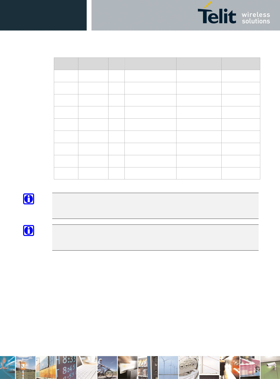
LE940B6 Hardware User Guide
1VV0301331 Rev. 1.8 - 2017-03-15
Reproduction forbidden without written authorization by Telit Communications S.p.A. - All Rights Reserved
Telit Confidential Information, provided under NDA Page
80 of 104
PAD Signal I/O Function Type Drive Strength
R18 GPIO_07 I/O Configurable GPIO CMOS 1.8V 3 mA
S19 GPIO_08 I/O Configurable GPIO CMOS 1.8V 3 mA
U19 GPIO_09 I/O Configurable GPIO CMOS 1.8V 3 mA
W19 GPIO_10 I/O Configurable GPIO CMOS 1.8V 3 mA
L18 GPIO_11 I/O Configurable GPIO CMOS 1.8V 3 mA
J18 GPIO_12 I/O Configurable GPIO CMOS 1.8V 3 mA
AN4 GPIO_20 I/O Configurable GPIO CMOS 1.8V 3 mA
H1 GPIO_21 I/O Configurable GPIO CMOS 1.8V 3 mA
K1 GPIO_22 I/O Configurable GPIO CMOS 1.8V 4 mA
NOTE:
To avoid a back-powering effect, it is recommended to avoid having any HIGH logic level signal
applied to the digital pins of the module when it is powered OFF or during an ON/OFF transition.
NOTE:
LE940B6 GPIOs can also be used as alternate I2C function. Refer to Section 8.3.2, I2C - Inter-
integrated Circuit.
8.6.1. Using a GPIO Pad as Input
GPIO pads, when used as inputs, can be connected to a digital output of another device and
report its status, provided this device has interface levels compatible with the 1.8V CMOS levels
of the GPIO.
If the digital output of the device is connected with the GPIO input, the pad has interface levels
different from the 1.8V CMOS. It can be buffered with an open collector transistor with a 10 kΩ
pull-up resistor to 1.8V.
8.6.2. Using a GPIO Pad as Output
GPIO pads, when used as outputs, can drive 1.8V CMOS digital devices or compatible hardware.
When set as outputs, the pads have a push-pull output, and therefore the pull-up resistor can be
omitted.

LE940B6 Hardware User Guide
1VV0301331 Rev. 1.8 - 2017-03-15
Reproduction forbidden without written authorization by Telit Communications S.p.A. - All Rights Reserved
Telit Confidential Information, provided under NDA Page
81 of 104
Figure 19: GPIO Output Pad Equivalent Circuit
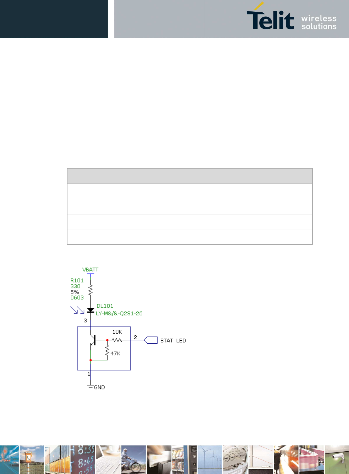
LE940B6 Hardware User Guide
1VV0301331 Rev. 1.8 - 2017-03-15
Reproduction forbidden without written authorization by Telit Communications S.p.A. - All Rights Reserved
Telit Confidential Information, provided under NDA Page
82 of 104
9. Miscellaneous Functions
9.1. Indication of Network Service Availability
The STAT_LED pin status shows information on the network service availability and call status.
In the LE940B6 module, the STAT_LED usually needs an external transistor to drive an external
LED.
The status indicated in Table 34 is configurable. Refer to Ref 1: LE940B6 AT Command Reference
Guide for the full description of this function.
Table 34: Network Service Availability Indication
LED Status Device Status
Permanently off Device off
Fast blinking (Period depends on network condition) Registered with power saving
Slow blinking (Period 3s, T
on
1s) Registered with full service
Permanently on A call is active
Figure 20: Status LED circuit example
LE940B6 Hardware User Guide
1VV0301331 Rev. 1.8 - 2017-03-15
Reproduction forbidden without written authorization by Telit Communications S.p.A. - All Rights Reserved
Telit Confidential Information, provided under NDA Page
83 of 104
9.2. RTC – Real Time Clock
The VRTC pin is used to power the RTC only when the main battery voltage level is too low or
missing.
9.3. VAUX Power Output
A regulated power supply output is provided to supply small devices from the module. This
output is active when the module is ON and goes OFF when the module is shut down. The
operating range characteristics of the supply are as follows:
Table 35: Operating Range – VAUX Power Supply
Min Typical Max
Output voltage 1.75V 1.80V 1.85V
Output current 100 mA
Output bypass capacitor (within the module)
1 μF
9.4. ADC Converter
9.4.1. Description
The LE940B6 module provides three on-board 12-bit Analog to Digital converters. Each ADC reads
the voltage level applied on the relevant pin, converts it and stores it into a 16-bit word.
Table 36: ADC Parameters
Min Max Units
Input voltage range 0 1.2 Volt
AD conversion - 12 bits
9.4.2. Using the ADC Converter
An AT command is available to use the ADC function.
The command is AT#ADC=1,2. The read value is expressed in mV.
Refer to Ref 1: LE940B6 AT Command Reference Guide for the full description of this function.
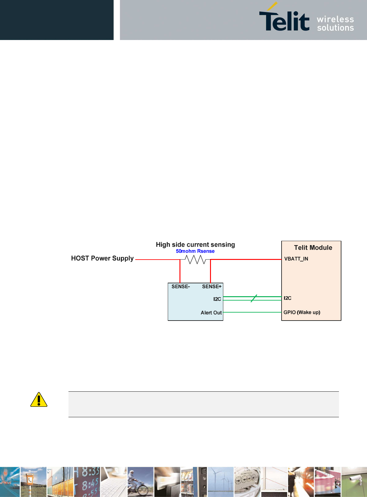
LE940B6 Hardware User Guide
1VV0301331 Rev. 1.8 - 2017-03-15
Reproduction forbidden without written authorization by Telit Communications S.p.A. - All Rights Reserved
Telit Confidential Information, provided under NDA Page
84 of 104
9.5. Using the Temperature Monitor Function
The Temperature Monitor supports temperature monitoring by giving periodic temperature
indications, to execute some function at extreme state. If properly set (see the #TEMPMON
command in the Ref 1: LE940B6 AT Command Reference Guide), it raises a GPIO to High Logic
level when the maximum temperature is reached.
9.6. Fuel Gauge (TBD)
The LE940B6 module can optionally support an external Fuel Gauge solution.
In this case, an external IC that is capable of measuring the current flow in and out of the module
must be added on the carrier board.
Figure 21 shows an example of a typical connectivity of such an external fuel gauge to the
LE940B6 module.
Detailed design - TBD
Figure 21: Fuel Gauge Connectivity Example
9.7. eFuse
The LE940B6 needs 1.8 +/- 0.05V applied on pad VPP(H17) for eFuses being programmed.
The fuse voltage should be applied to VPP(H17) prior to the fuse script being started, and should
be removed after the fuse operation has been completed.
Warning:
Fuse voltage must never be supplied when the module is not powered up.
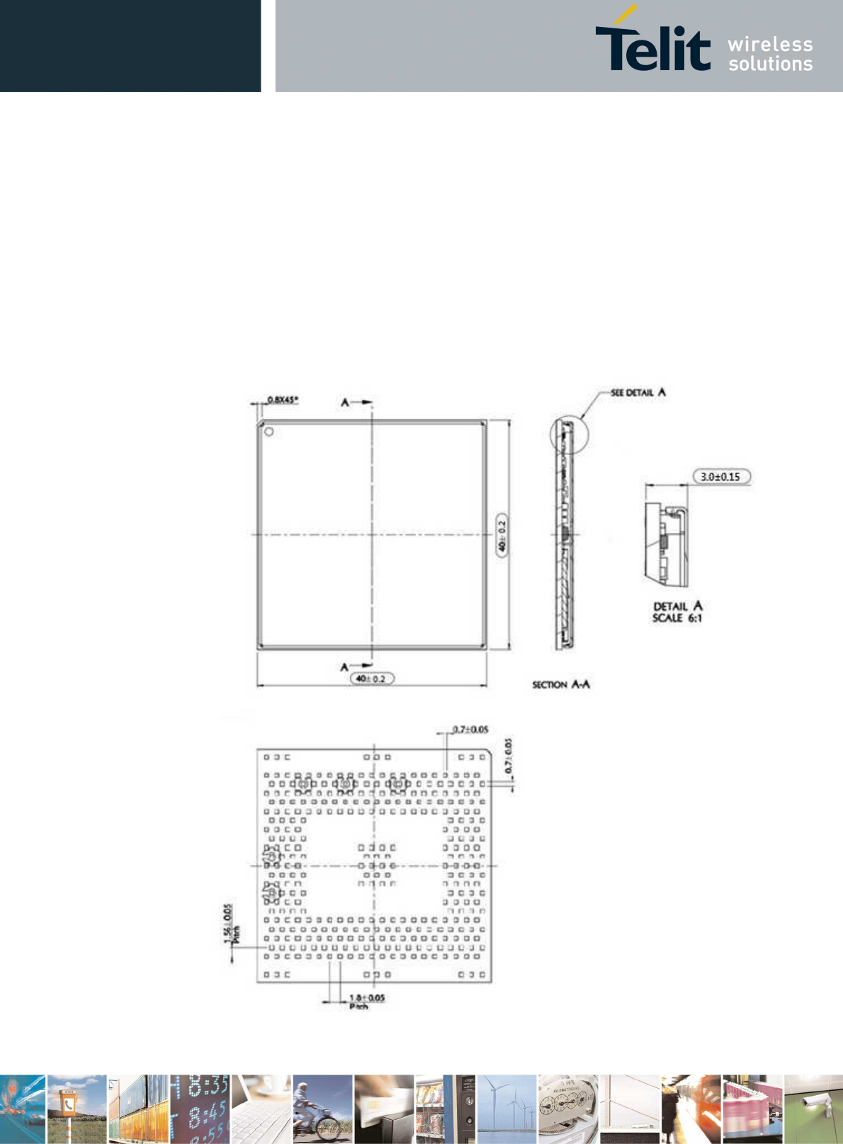
LE940B6 Hardware User Guide
1VV0301331 Rev. 1.8 - 2017-03-15
Reproduction forbidden without written authorization by Telit Communications S.p.A. - All Rights Reserved
Telit Confidential Information, provided under NDA Page
85 of 104
10. Mounting the Module on your Board
10.1. General
The LE940B6 module is designed to be compliant with a standard lead-free soldering process as
defined in JESD22b102d, table 3b. The number of reflows must not exceed two. This limits Tmax
to 245 °C.
10.2. Finishing & Dimensions
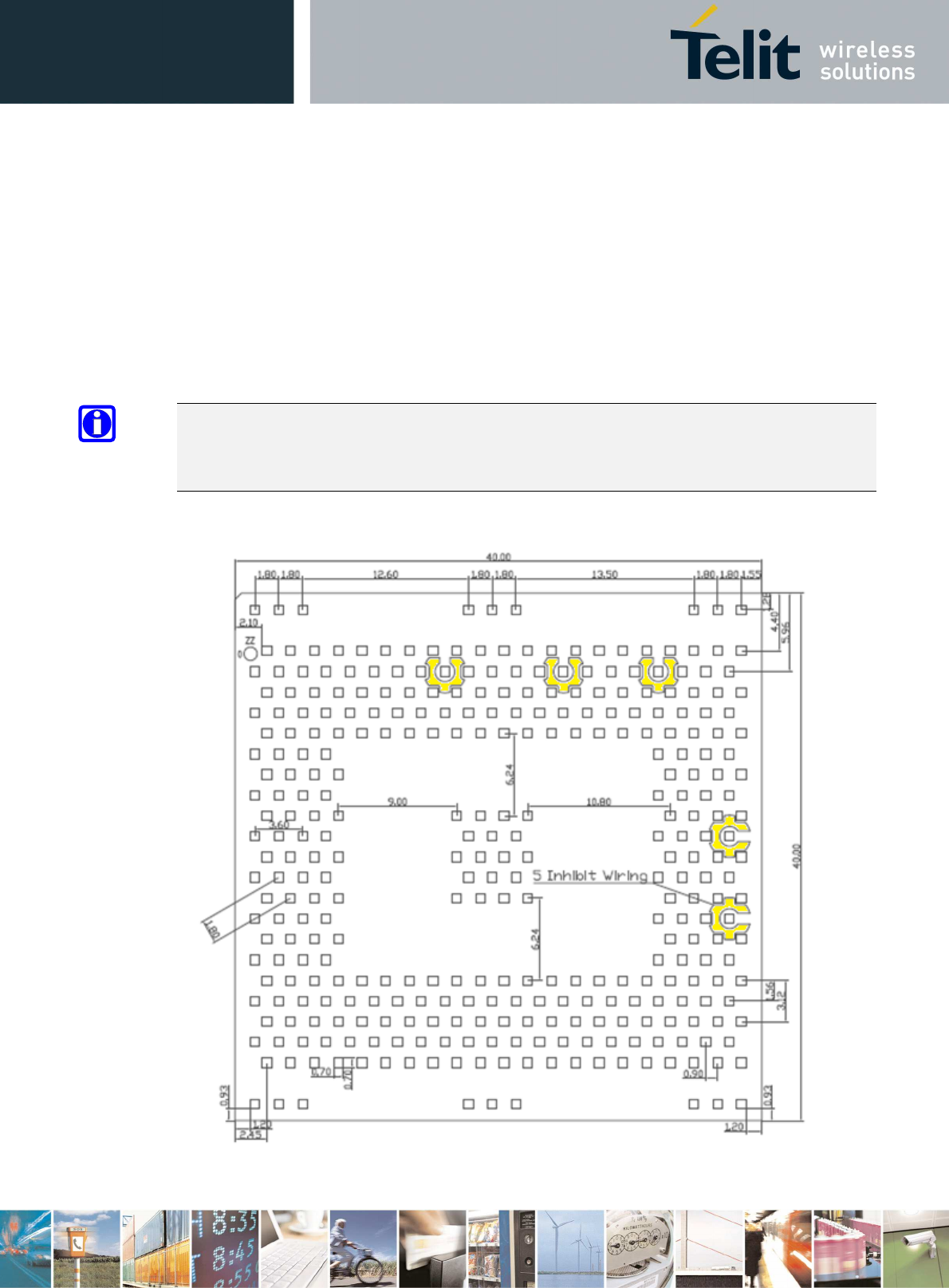
LE940B6 Hardware User Guide
1VV0301331 Rev. 1.8 - 2017-03-15
Reproduction forbidden without written authorization by Telit Communications S.p.A. - All Rights Reserved
Telit Confidential Information, provided under NDA Page
86 of 104
10.3. Recommended Footprint for the Application
Figure 22 shows the top view of the module, which has 334 pads (dimensions are in mm).
To facilitate replacing the LE940B6 module if necessary, it is suggested to design the application
board with a 1.5 mm placement inhibit area around the module. These regions are highlighted in
Figure 22.
It is also suggested, as a common rule for an SMT component, to avoid having a mechanical part
of the application board in direct contact with the module.
NOTE:
In the customer application, the region marked as INHIBIT WIRING in Figure 22 must be clear of
signal wiring or ground polygons.
Figure 22: Application Module Top View
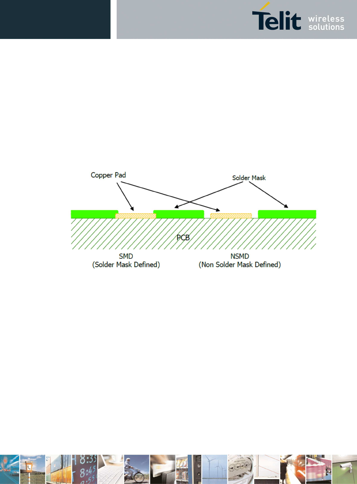
LE940B6 Hardware User Guide
1VV0301331 Rev. 1.8 - 2017-03-15
Reproduction forbidden without written authorization by Telit Communications S.p.A. - All Rights Reserved
Telit Confidential Information, provided under NDA Page
87 of 104
10.4. Stencil
Stencil’s apertures layout can be the same as the recommended footprint (1:1). The suggested
thickness of stencil foil is greater than 120 µm.
10.5. PCB Pad Design
The solder pads on the PCB are recommended to be of the Non Solder Mask Defined (NSMD)
type.
Figure 23: PCB Pad Design
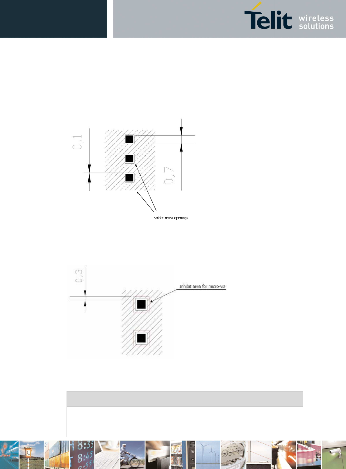
LE940B6 Hardware User Guide
1VV0301331 Rev. 1.8 - 2017-03-15
Reproduction forbidden without written authorization by Telit Communications S.p.A. - All Rights Reserved
Telit Confidential Information, provided under NDA Page
88 of 104
10.6. Recommendations for PCB Pad Dimensions (mm)
Figure 24: PCB Pad Dimensions
It is not recommended to place around the pads a via or micro-via that is not covered by solder
resist in an area of 0.3 mm unless it carries the same signal as the pad itself (see Figure 25).
Figure 25: Inhibit Area for Micro-via
Holes in pad are allowed only for blind holes and not for through holes.
Table 37: Recommendations for PCB Pad Surfaces
Finish Layer Thickness (um)
Properties
Electro-less Ni / Immersion Au 3-7 / 0.05-0.15 Good solder ability
protection, high shear force
values
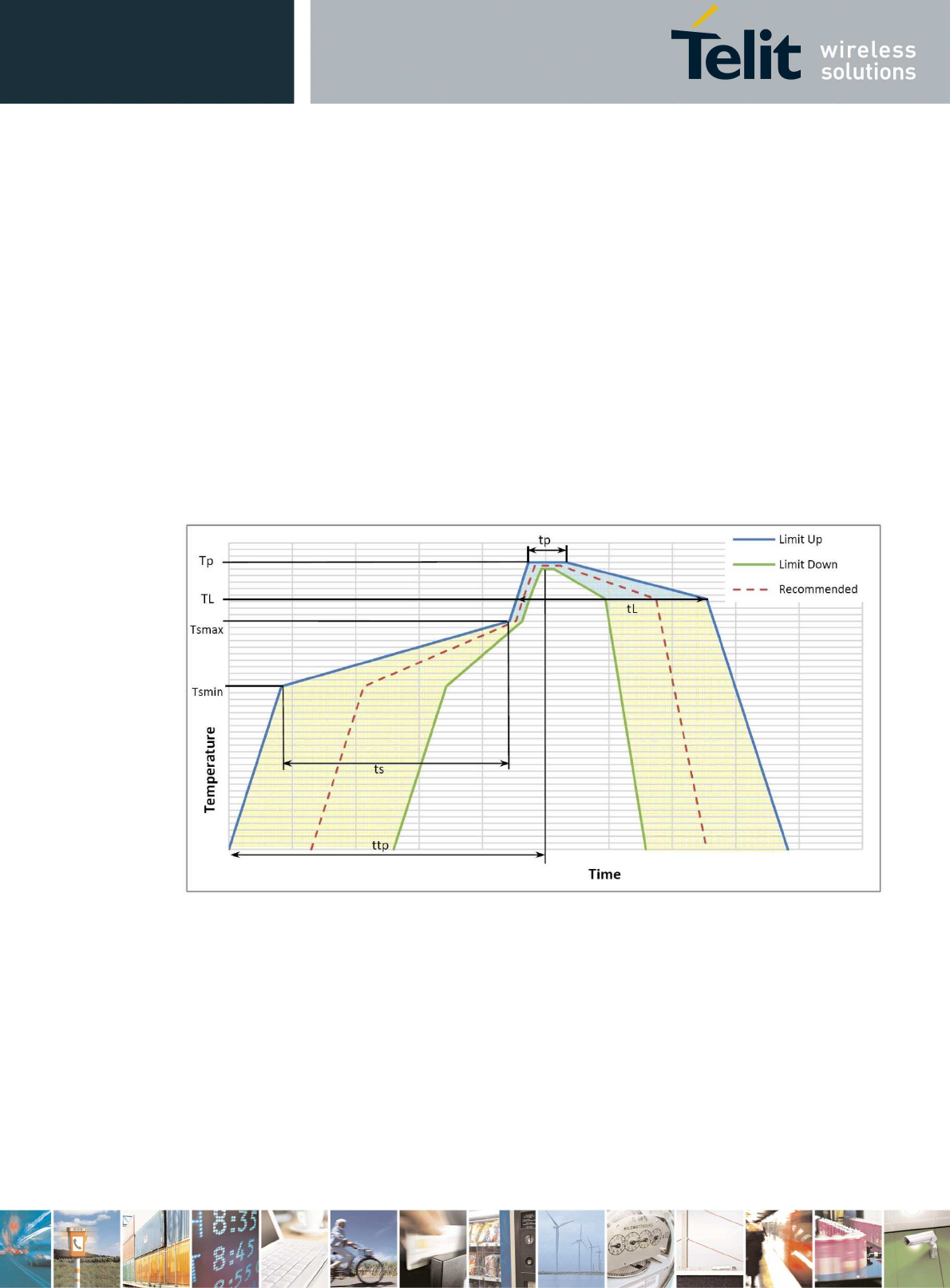
LE940B6 Hardware User Guide
1VV0301331 Rev. 1.8 - 2017-03-15
Reproduction forbidden without written authorization by Telit Communications S.p.A. - All Rights Reserved
Telit Confidential Information, provided under NDA Page
89 of 104
The PCB must be able to resist the higher temperatures, which occur during the lead-free process.
This issue should be discussed with the PCB-supplier. Generally, the wettability of tin-lead solder
paste on the described surface plating is better compared to lead-free solder paste.
10.7. Solder Paste
We recommend using only “no clean” solder paste to avoid the cleaning of the modules after
assembly.
10.7.1. Solder Reflow
Figure 26 shows the recommended solder reflow profile.
Figure 26: Solder Reflow Profile
LE940B6 Hardware User Guide
1VV0301331 Rev. 1.8 - 2017-03-15
Reproduction forbidden without written authorization by Telit Communications S.p.A. - All Rights Reserved
Telit Confidential Information, provided under NDA Page
90 of 104
Table 38: Solder Profile Characteristics
Profile Feature Pb-Free Assembly
Average ramp-up rate (T
L
to T
P
) 3°C/second max
Preheat
– Temperature min (Tsmin)
– Temperature max (Tsmax)
– Time (min to max) (ts)
150°C
200°C
60-180 seconds
Tsmax to TL
– Ramp-up rate
3°C/second max
Time maintained above:
– Temperature (TL)
– Time (tL)
217°C
60-150 seconds
Peak temperature (Tp) 245 +0/-5°C
Time within 5°C of actual peak
Temperature (tp)
10-30 seconds
Ramp-down rate 6°C/second max
Time 25°C to peak temperature 8 minutes max
NOTE:
All temperatures refer to topside of the package, measured on the package body surface.
Warning:
The LE940B6 module withstands one reflow process only.

LE940B6 Hardware User Guide
1VV0301331 Rev. 1.8 - 2017-03-15
Reproduction forbidden without written authorization by Telit Communications S.p.A. - All Rights Reserved
Telit Confidential Information, provided under NDA Page
91 of 104
11. Application Guide
11.1. Debug of the LE940B6 Module in Production
To test and debug the mounting of the LE940B6 module, we strongly recommend to add several
test pads on the application board design for the following purposes:
• Checking the connection between the LE940B6 itself and the application
• Testing the performance of the module by connecting it with an external computer
Depending on the customer application, these test pads include, but are not limited to the
following signals:
• TXD
• RXD
• ON_OFF_N
• SHUTDOWN_N
• RESET_N
• GND
• VBATT
• VAUX/PWRMON
• TXD_AUX
• RXD_AUX
• USB_VBUS
• USB_D+
• USB_D-
• Signals for analysis

LE940B6 Hardware User Guide
1VV0301331 Rev. 1.8 - 2017-03-15
Reproduction forbidden without written authorization by Telit Communications S.p.A. - All Rights Reserved
Telit Confidential Information, provided under NDA Page
92 of 104
11.2. Bypass Capacitor on Power Supplies
When a sudden voltage step is asserted to or a cut from the power supplies, the steep transition
causes some reactions such as overshoot and undershoot. This abrupt voltage transition can
affect the device causing it to not operate or to malfunction.
Bypass capacitors are needed to alleviate this behavior. The behavior can appear differently
depending on the various applications. Customers must pay special attention to this issue when
they design their application board.
The length and width of the power lines must be considered carefully and the capacitance of the
capacitors must be selected accordingly.
The capacitor will also prevent ripple of the power supplies and the switching noise caused in
TDMA systems.
Especially, a suitable bypass capacitor must be mounted on the following lines on the application
board:
• VBATT & VBATT_PA (Pads AP17,AP19,AR18,AR20,AS17,AS19,AT18,AU17,AU19,AT20)
Recommended values are:
• 100 uF for VBATT & VBATT_PA
Customers must still consider that the capacitance mainly depends on the conditions of their
application board.
Generally, more capacitance is required when the power line is longer.
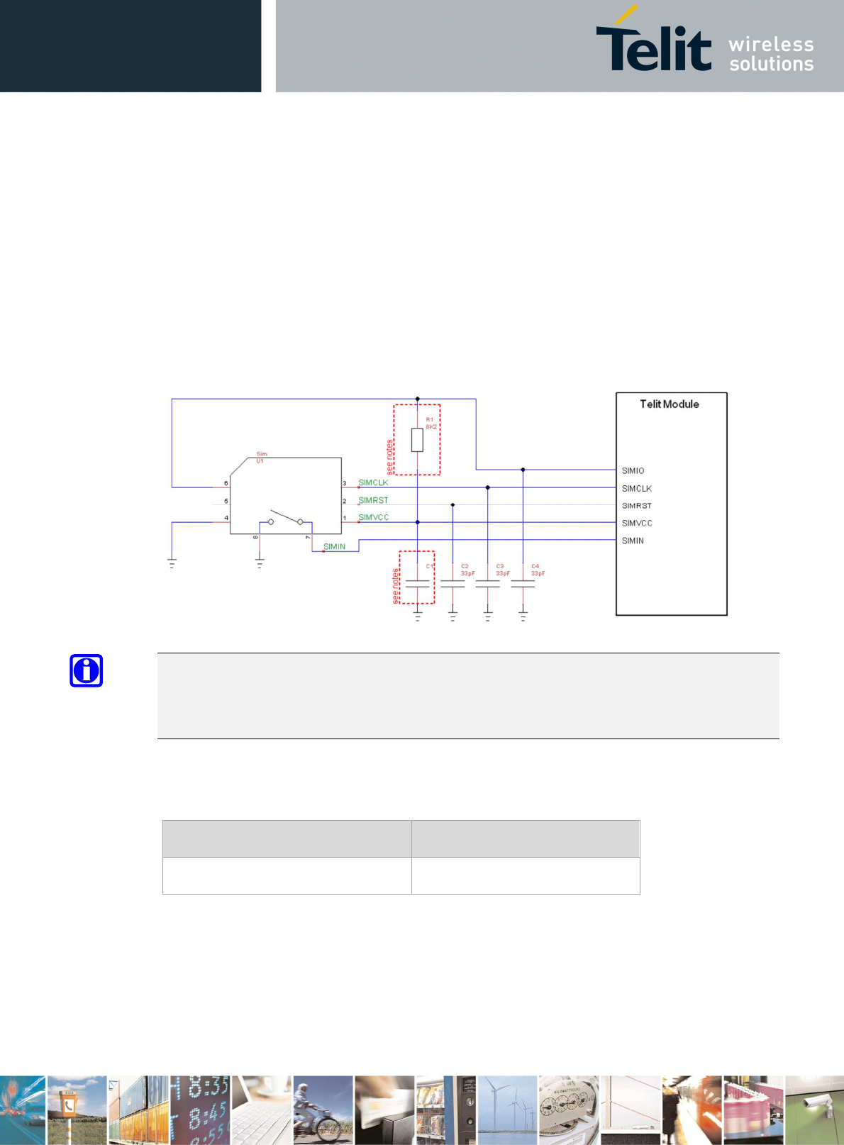
LE940B6 Hardware User Guide
1VV0301331 Rev. 1.8 - 2017-03-15
Reproduction forbidden without written authorization by Telit Communications S.p.A. - All Rights Reserved
Telit Confidential Information, provided under NDA Page
93 of 104
11.3. SIM Interface
This section presents the recommended schematics for the design of SIM interfaces on the
application boards. The LE940B6 supports two external SIM interfaces.
11.3.1. SIM Schematic Example
Figure 27 illustrates in particular how to design the application side, and what values the
components should have.
Figure 27: SIM Schematics
NOTE:
An external pull-up resistor on SIMIO is not required.
The LE940B6 module contains an internal pull-up resistor on SIMIO.
Table 39 lists the values of C1 to be adopted with the LE940B6 product:
Table 39: SIM Interface – C1 Range
Product P/N C1 Range (nF)
LE940B6 100 nF
Refer to the following document for details:
• Ref 4: SIM Integration Design Guide
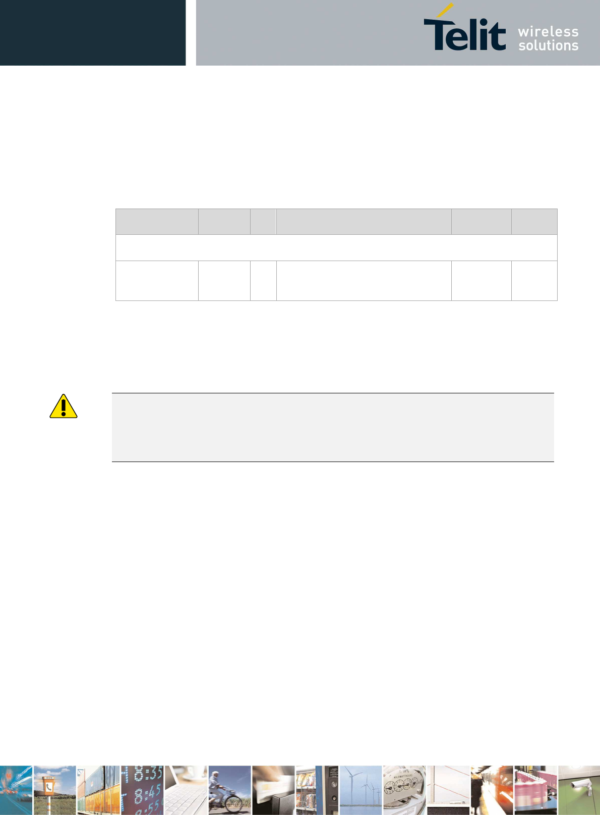
LE940B6 Hardware User Guide
1VV0301331 Rev. 1.8 - 2017-03-15
Reproduction forbidden without written authorization by Telit Communications S.p.A. - All Rights Reserved
Telit Confidential Information, provided under NDA Page
94 of 104
11.4. EMC Recommendations
All LE940B6 signals are provided with some EMC protection. Nevertheless, the accepted level
differs according to the specific pin. Table 40 lists the characteristics.
Table 40: EMC Recommendations
Pad Signal I/O
Function Contact Air
Antenna
AD1, AU9 Antenna
pads
I/O
Antenna pads ± 4 KV ± 8 KV
All other pins have the following characteristics:
• HBM JESD22-A114-B ± 1000 V
• CDM JESD22-C101-C ± 250 V
Warning:
Do not touch without proper electrostatic protective equipment. The product must be handled
with care, avoiding any contact with the pins because electrostatic discharge may damage the
product.
11.5. Download and Debug Port
This section provides recommendations for the design of the host system used to download or
upgrade the Telit software and to debug the LE940B6 module when it is already mounted on a
host system.
• For downloading or upgrading the Telit software
In the LE940B6 module, firmware updates by the host are only possible via USB and not via
UART.
So even if USB interface is not used, it is still highly recommended to place an optional USB
connector on the application board.At the minimum, test points of the USB signals are
required to enable SW update.
• For debugging of the LE940B6 module
USB, Auxiliary UART and JTAG interfaces can be used for debugging the LE940B6 module.
Even if USB or JTAG are not used for debugging, it is recommended to have at least the
Auxiliary UART pins exposed to outside for debugging purposes.

LE940B6 Hardware User Guide
1VV0301331 Rev. 1.8 - 2017-03-15
Reproduction forbidden without written authorization by Telit Communications S.p.A. - All Rights Reserved
Telit Confidential Information, provided under NDA Page
95 of 104
11.6. Antenna Detection
The LE940B6 module provides an antenna detection application.
Many automotive applications require to detect if the antenna is shorted to ground or the battery
of the vehicle for fault tracing. Basically, antenna detection is performed by means of its DC
characteristics, splitting the DC and RF paths.
Refer to Telit 80000NT10002a - Antenna Detection Application Note.

LE940B6 Hardware User Guide
1VV0301331 Rev. 1.8 - 2017-03-15
Reproduction forbidden without written authorization by Telit Communications S.p.A. - All Rights Reserved
Telit Confidential Information, provided under NDA Page
96 of 104
12. Packing System
The LE940B6 module is packed on trays.
The tray is JEDEC compliant, injection molded antistatic Modified Polyphenylene ether (MPPO). It
has good thermal characteristics and can withstand the standard baking temperature of up to
125°C, thereby avoiding the need of handling the modules if baking is required. The trays are
rigid, thus providing mechanical protection against transport stress. In addition, they are re-
usable and so environmentally sustainable.
There are 2 (two) antistatic rubber bands that enclose each envelope.
The carton box is rigid, thus offering mechanical protection. The carton box has one flap across
the entire top surface. It is sealed with tape along the edges of the box.
Table 41: Tray Packing
Modules per
Tray
Trays per
Envelope
Modules per
Envelope
Envelopes per
Carton Box
Modules per
Box
21 5+ 1 empty 105 4 420
Table 42: Packing Quantities
Order Type Quantity
Minimum Order Quantity (MOQ) 21
Standard Packing Quantity (SPQ) 420
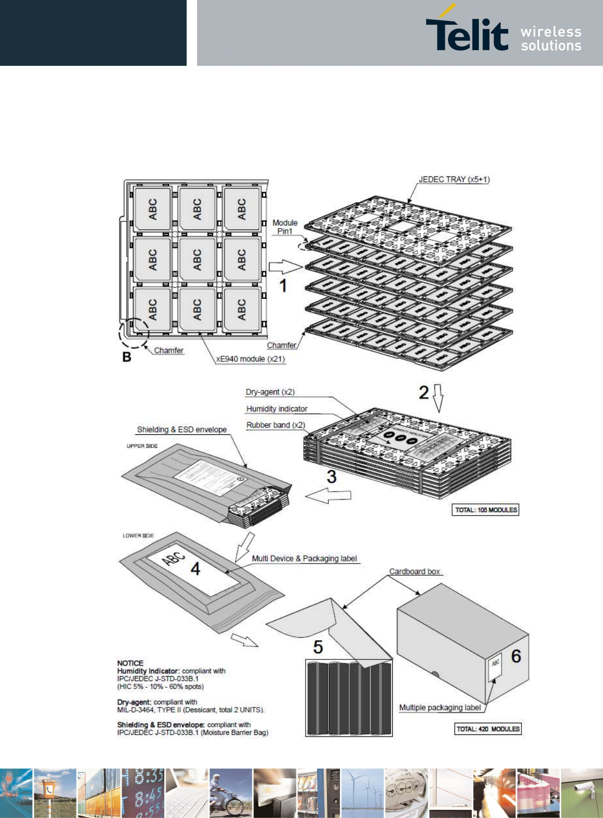
LE940B6 Hardware User Guide
1VV0301331 Rev. 1.8 - 2017-03-15
Reproduction forbidden without written authorization by Telit Communications S.p.A. - All Rights Reserved
Telit Confidential Information, provided under NDA Page
97 of 104
Each tray contains 24 modules as shown in Figure 28.
Figure 28: Tray Packing
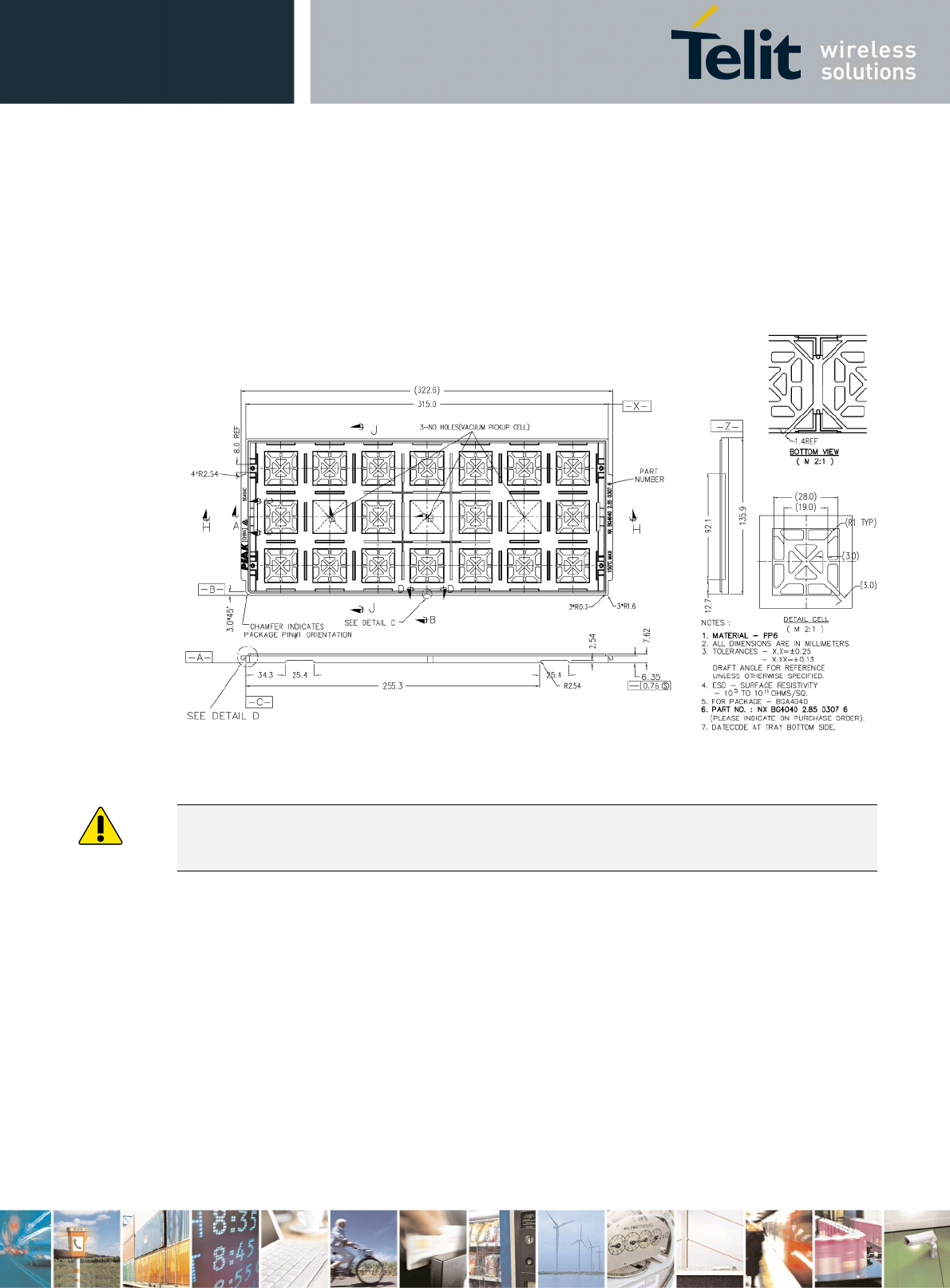
LE940B6 Hardware User Guide
1VV0301331 Rev. 1.8 - 2017-03-15
Reproduction forbidden without written authorization by Telit Communications S.p.A. - All Rights Reserved
Telit Confidential Information, provided under NDA Page
98 of 104
12.1. Tray Drawing
The Telit LE940B6 is packaged on trays. Each tray contains 21 pieces with the following
dimensions:
Figure 29: Tray Drawing
Warning:
These trays can withstand a maximum temperature of 125°C
12.2. Moisture Sensitivity
The LE940B6 module is a Moisture Sensitive Device Level 3, in accordance with standard
IPC/JEDEC J-STD-020. Observe all of the requirements for using this kind of components.
Calculated shelf life in sealed bag: 4 months at <40°C and <90% relative humidity (RH).

LE940B6 Hardware User Guide
1VV0301331 Rev. 1.8 - 2017-03-15
Reproduction forbidden without written authorization by Telit Communications S.p.A. - All Rights Reserved
Telit Confidential Information, provided under NDA Page
99 of 104
13. Conformity Assessment Issues
13.1. FCC/IC Regulatory Notices
Manual Information to the End User
The OEM integrator has to be aware not to provide information to the end user regarding
how to install or remove this RF module in the user’s manual of the end product which
integrates this module. The end user manual shall include all required regulatory
information/warning as show in this manual.
CAN ICES-3(B)/ NMB-3(B)
Federal Communication Commission Interference Statement
This device complies with Part 15 of the FCC Rules. Operation is subject to the following two
conditions: (1) This device may not cause harmful interference, and (2) this device must
accept any interference received, including interference that may cause undesired operation.
This device complies with Industry Canada’s licence-exempt RSSs. Operation is subject to the
following two conditions:
(1) This device may not cause interference; and
(2) This device must accept any interference, including interference that may cause undesired
operation of the device.
Le présent appareil est conforme aux CNR d'Industrie Canada applicables aux appareils radio
exempts de licence. L'exploitation est autorisée aux deux conditions suivantes:
(1) l'appareil ne doit pas produire de brouillage, et
(2) l'utilisateur de l'appareil doit accepter tout brouillage radioélectrique subi, même si le
brouillage est susceptible d'en compromettre le fonctionnement."
This equipment has been tested and found to comply with the limits for a Class B digital
device, pursuant to Part 15 of the FCC Rules. These limits are designed to provide reasonable
protection against harmful interference in a residential installation. This equipment
generates, uses and can radiate radio frequency energy and, if not installed and used in
accordance with the instructions, may cause harmful interference to radio communications.
However, there is no guarantee that interference will not occur in a particular installation. If
this equipment does cause harmful interference to radio or television reception, which can be
determined by turning the equipment off and on, the user is encouraged to try to correct the
interference by one of the following measures:
- Reorient or relocate the receiving antenna.
- Increase the separation between the equipment and receiver.

LE940B6 Hardware User Guide
1VV0301331 Rev. 1.8 - 2017-03-15
Reproduction forbidden without written authorization by Telit Communications S.p.A. - All Rights Reserved
Telit Confidential Information, provided under NDA Page
100 of 104
- Connect the equipment into an outlet on a circuit different from that to which the receiver is
connected.
- Consult the dealer or an experienced radio/TV technician for help.
Any changes or modifications not expressly approved by the party responsible for compliance
could void the user's authority to operate this equipment. This transmitter must not be co-
located or operating in conjunction with any other antenna or transmitter.
Radiation Exposure Statement
This equipment complies with FCC/IC radiation exposure limits set forth for an uncontrolled
environment. This equipment should be installed and operated with minimum distance 20 cm
between the radiator & your body.
End Product Labeling
When the module is installed in the host device, the FCC/IC ID label must be visible through a
window on the final device or it must be visible when an access panel, door or cover is easily
re-moved. If not, a second label must be placed on the outside of the final device that
contains the following text: “Contains FCC ID: RI7LE940B6NA”, “Contains IC: 5131A-
LE940B6NA.” The grantee's FCC/IC ID can be used only when all FCC/IC compliance
requirements are met.
This device is intended only for OEM integrators under the following conditions:
(1) The antenna must be installed such that 20 cm is maintained between the antenna and
users,
(2) The transmitter module may not be co-located with any other transmitter or antenna.
(3) To comply with FCC/IC regulations limiting both maximum RF output power and human
exposure to RF radiation, the maximum antenna gain including cable loss in a mobile
exposure condition must not exceed:
3.0 dBi in Cellular band
3.5 dBi in PCS band
3.5 dBi in AWS band
3.0 dBi in 700 MHz band
4.0 dBi in 2500MHz band
In the event that these conditions cannot be met (for example certain laptop configurations
or co-location with another transmitter), then the FCC/IC authorization is no longer
considered valid and the FCC/IC ID cannot be used on the final product. In these
circumstances, the OEM integrator will be responsible for re-evaluating the end product
(including the transmitter) and obtaining a separate FCC/IC authorization.

LE940B6 Hardware User Guide
1VV0301331 Rev. 1.8 - 2017-03-15
Reproduction forbidden without written authorization by Telit Communications S.p.A. - All Rights Reserved
Telit Confidential Information, provided under NDA Page
101 of 104
14. Safety Recommendations
READ CAREFULLY
Be sure that the use of this product is allowed in your country and in the environment required.
The use of this product may be dangerous and must be avoided in the following areas:
• Where it can interfere with other electronic devices in environments such as hospitals,
airports, aircrafts, etc.
• Where there is risk of explosion, such as gasoline stations, oil refineries, etc.
It is the responsibility of the user to enforce the country regulations and the specific environment
regulations.
Do not disassemble the product; any mark of tampering will compromise the warranty validity.
We recommend following the instructions of the hardware user guides for correct wiring of the
product. The product must be supplied with a stabilized voltage source and the wiring conform to
the security and fire prevention regulations.
The product must be handled with care, avoiding any contact with the pins because electrostatic
discharges may damage the product itself. The same caution must be taken for the SIM, checking
carefully the instructions for its use. Do not insert or remove the SIM when the product is in
power saving mode.
The system integrator is responsible for the functioning of the final product; therefore, care must
be taken of the external components of the module, as well as of any project or installation issue,
because of the risk of disturbing the cellular network or external devices or having any impact on
safety. Should there be any doubt, refer to the technical documentation and the regulations in
force.
Every module must be equipped with a proper antenna with the specified characteristics. The
antenna must be installed with care to avoid any interference with other electronic devices and
must be installed with the guarantee of a minimum 20 cm distance from a human body. If this
requirement cannot be satisfied, the system integrator must assess the final product against the
SAR regulation.
The European Community provides some Directives for electronic equipment introduced on the
market. All the relevant information is available on the European Community website:
http://europa.eu.int/comm/enterprise/rtte/dir99-5.htm
The text of the Directive 99/05 regarding telecommunication equipment is available, while the
applicable Directives (Low Voltage and EMC) are available at:
http://europa.eu.int/comm/enterprise/rtte/dir99-5.htm

LE940B6 Hardware User Guide
1VV0301331 Rev. 1.8 - 2017-03-15
Reproduction forbidden without written authorization by Telit Communications S.p.A. - All Rights Reserved
Telit Confidential Information, provided under NDA Page
102 of 104
15. Document History
Table 43: Document Revision History
Revision Date Changes
Rev. 1.8 2017-03-10
Sec. 5.1: Added Note
Sec. 5.3: Added Note
Sec. 6.1: Updated table 21 LE940B6 Current Consumption
Sec. 7.5: Added new sub chapter
Sec. 13: Added Conformity Assessment Issues
Rev. 1.7 2017-01-25
Sec. 5: Figures and charts revised
Sec. 6: Current consumption table updated

LE940B6 Hardware User Guide
1VV0301331 Rev. 1.8 - 2017-03-15
Reproduction forbidden without written authorization by Telit Communications S.p.A. - All Rights Reserved
Telit Confidential Information, provided under NDA Page
103 of 104
Revision Date Changes
v. 1.6 2016-11-15
Official Release
Sec. 2.7: Updated the Mechanical Specifications
Sec. 3.1: Added VPP pin for eFuse
Sections 3.1, 3.3, 4.3.6, 8: SD / MMC interfaces were deleted - they
are not supported by the chipset vendor.
Sec. 5: Updated the specifications and charts of Hardware
Commands (Boot-up/Shutdown time, On/Shutdown key hold
time)
Sec. 5.1: Updated the Power on Hold time.
Sec. 5.3.2: Updated the section of Hardware Shutdown
Sec. 5.3.3: Updated the Unconditional reset Hold time.
Sec. 6.1: Updated Table 21 – Current Consumption in various
modes
Sec. 6.2.2: Updated the Thermal Design Guidelines
Sec. 8.1: USB 3.0 interface is deleted - it is not supported by the
chipset vendor.
Sec. 8.3.3: WiFi (SDIO) is deleted - it is not supported by the
chipset vendor.
Sec. 8.6: Table 35 (Additional GPIO) is deleted - it is not supported
by the chipset vendor.
Sec. 9.7: eFuse section was added.
Sec. 11.4: Updated the EMC Recommendations

LE940B6 Hardware User Guide
1VV0301331 Rev. 1.8 - 2017-03-15
Reproduction forbidden without written authorization by Telit Communications S.p.A. - All Rights Reserved
Telit Confidential Information, provided under NDA Page
104 of 104
Revision Date Changes
Rev. 1.5 2016-09-20
(Interim version)
Page 2, Table 1: Updated the Applicability table
Sec. 2: Updated the General Product Description
Sec. 2.5.1, 2.5.2: Updated the RF bands tables
Sec. 3.1: Updated the pin description in the Pin-out table
Sec. 4.3: Added tables of logic level specifications
Sec. 5: Updated the Turning On and Off trigger times, figures and
flow charts
Sec. 6.1: Added Table 20 - Power Supply Requirements
Sec. 8: Gathered the description of all hardware interfaces into
this section
Sec. 8.1: Updated note and figure for USB
Sec: 8.2: Various updates about the Serial Ports
Sec. 8.4: Updates about the Ethernet interface
Sec. 8.6: Updated the GPIO drive strength
Sec 11.5: Updated the Download and Debug Port section
Sec 12: Updated Packing System information
Rev. 1.3 2016-06-22
(Interim version)
Sec. 2.4.1: The Storage Temperature range is –40°C ~ +95°C
Sec. 3.1: Corrected and Updated the Pin out table
(Added GPIO_11/12, MIC_BIAS, VRTC, Removed GPIO_23/24)
Sec. 4: Added electrical specifications
Sec. 9.4.1: Modified the ADC table
Sec. 11.4: Added ESD specifications
Preliminary
2016-03-15
First issue