Telit Communications S p A ME910C1NA ME910C1-NA LTE Module CAT M User Manual Users guide
Telit Communications S.p.A. ME910C1-NA LTE Module CAT M Users guide
UserManual.wiki
>
Telit Communications S p A
>
ME910C1NA User Manual
>
Users guide
Contents
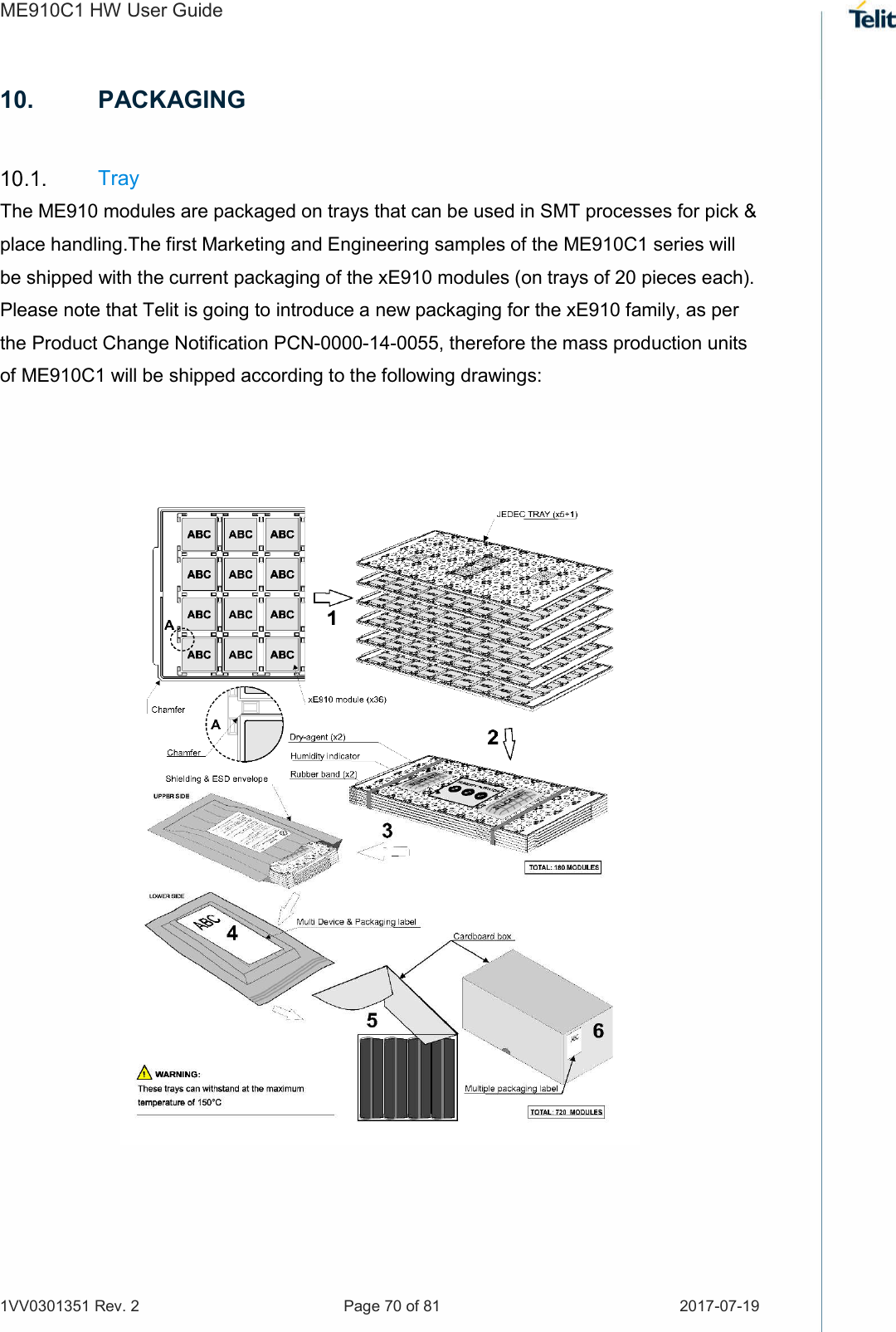
1.
Users guide
2.
Users manual
Users guide
Navigation menu
Upload a User Manual
Namespaces
Wiki Guide
HTML
PDF
Info
Views
User Manual
Discussion / Help
Navigation
![[04.2016] Mod. 0805 2016-08 Rev.5 ME910C1 HW User Guide 1VV03001351 Rev. 2 – 2017-07-19](https://usermanual.wiki/Telit-Communications-S-p-A/ME910C1NA.Users-guide/User-Guide-3493560-Page-1.png)
![[04.2016] Mod. 0805 2016-08 Rev.5](https://usermanual.wiki/Telit-Communications-S-p-A/ME910C1NA.Users-guide/User-Guide-3493560-Page-81.png)