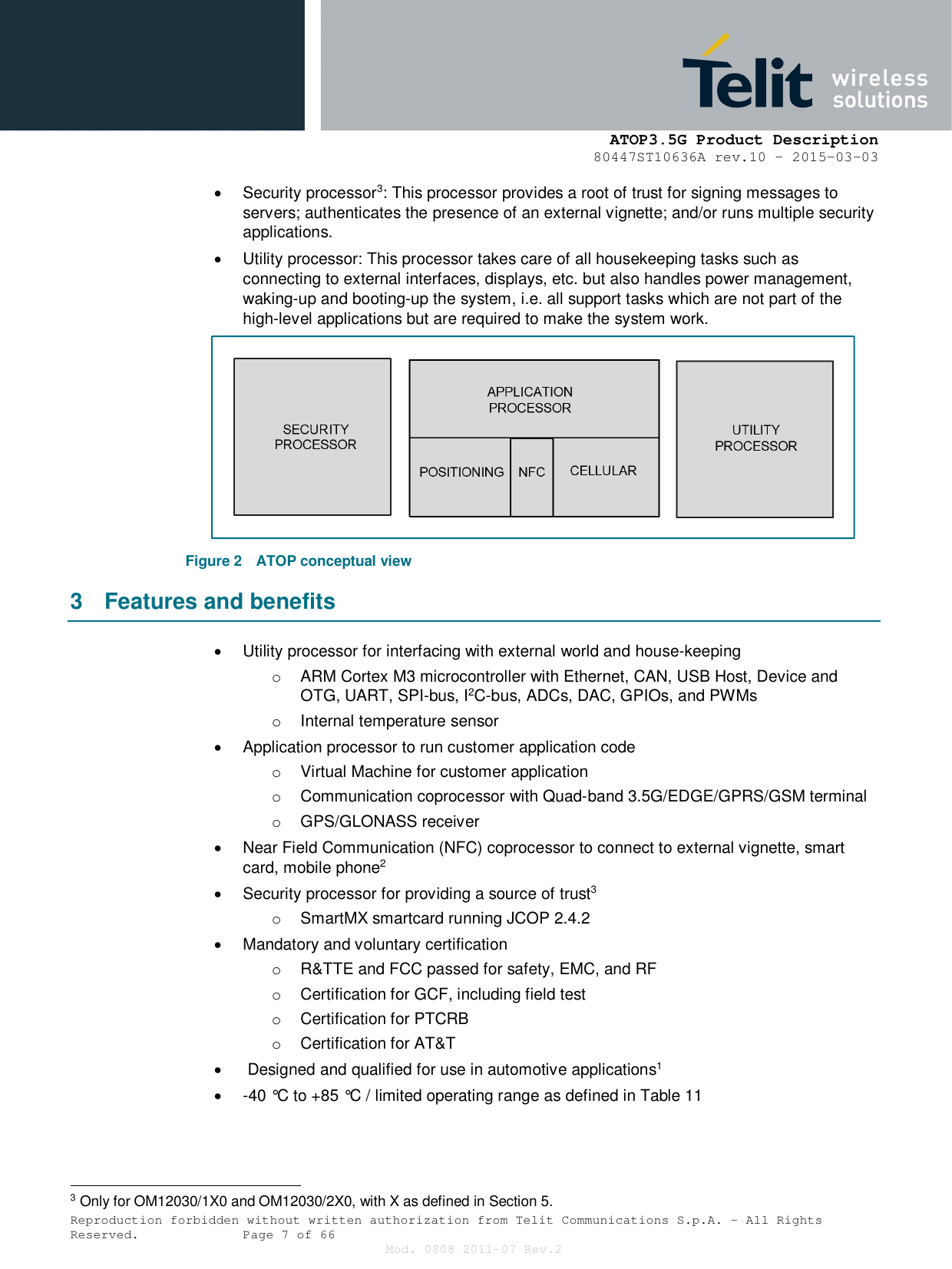
Telit Communications S p A OM12030-210 2G/3.5G wireless module User Manual User guide
Telit Communications S.p.A. 2G/3.5G wireless module User guide
UserManual.wiki
>
Telit Communications S p A
>
OM12030 210 User Manual
User guide
Navigation menu
Upload a User Manual
Namespaces
Wiki Guide
HTML
PDF
Info
Views
User Manual
Discussion / Help
Navigation
![ATOP3.5G Product Description 80447ST10636A rev.10 – 2015-03-03 Reproduction forbidden without written authorization from Telit Communications S.p.A. - All Rights Reserved. Page 8 of 66 Mod. 0808 2011-07 Rev.2 4 Applications ATOP 3.5G can be used for telematics applications where tamper-resistance, confidentiality, integrity and authenticity of end-user information are required, e.g.: Road pricing Pay as you drive insurance Stolen vehicles tracking Emergency call Internet connectivity 5 Ordering information ATOP 3.5G is defined in multiple variants: Table 1 Type names Type number Package Name Description OM12030/X00 [1] LGA350 Worldwide Quad-band UMTS 2100 (I), 1900 (II), 850 (V) including 800 (VI), 900 (VIII) OM12030/X10 [1] North American Quad-band UMTS 2100 (I), 1900 (II), 1700 (IV), 850 (V) including 800 (VI) OM12030/X20 [1] Pacific Quad-band UMTS 2100 (I), 1800 (III) including 1700 (IX), 850 (V) including 800 (VI), 900 (VIII) [1] X = 1 Includes NFC short range communication and the SmartMX security element. Feature combination nicknamed “Full”. X = 0 Omits NFC short range communication and the SmartMX security element. Feature combination nicknamed “Minus”. X = 2 Omits NFC short range communication but retains the SmartMX security element. Feature combination nicknamed “Auth”. All variants support 2G bands 850, 900, 1800, and 1900.](https://usermanual.wiki/Telit-Communications-S-p-A/OM12030-210/User-Guide-2560823-Page-8.png)
![ATOP3.5G Product Description 80447ST10636A rev.10 – 2015-03-03 Reproduction forbidden without written authorization from Telit Communications S.p.A. - All Rights Reserved. Page 10 of 66 Mod. 0808 2011-07 Rev.2 7 Pinning information 7.1 Pinning Figure 4 shows a transparent top view of ATOP 3.5G to identify all pins. Figure 4 ATOP 3.5G pin configuration 7.2 Pin description 7.2.1 Module pinning list Table 2 ATOP 3.5G pinning list Symbol[1] Pin Level Description[2] Utility processor UART0 MC_P002_TXD0_AD07 M15 3.0 transmitter output for UART0 [3] MC_P003_RXD0_AD06 M19 3.0 receiver input for UART0 [3] UART1 MC_P015_TXD1_SCK0_SCK V15 3.0 transmitter output for UART1 [4][5] MC_P016_RXD1_SSEL0_SSEL T7 3.0 receiver input for UART1 [4][5] MC_P022_RTS1_TD1 T9 3.0 ready to send [5] MC_P017_CTS1_MISO0_MISO V13 3.0 clear to send [4][5] MC_P021_RI1_RD1 R10 3.0 ring indicator [5] MC_P018_DCD1_MOSI0_MOSI R11 3.0 data carrier detect [4][5] UART2 MC_P010_TXD2_SDA2_MAT30 R13 3.0 transmitter output for UART2 [5] MC_P011_RXD2_SCL2_MAT31 U10 3.0 receiver input for UART2 [5]](https://usermanual.wiki/Telit-Communications-S-p-A/OM12030-210/User-Guide-2560823-Page-10.png)
![ATOP3.5G Product Description 80447ST10636A rev.10 – 2015-03-03 Reproduction forbidden without written authorization from Telit Communications S.p.A. - All Rights Reserved. Page 11 of 66 Mod. 0808 2011-07 Rev.2 Symbol[1] Pin Level Description[2] UART3 MC_P428_RXMCLK_MAT20_TXD3 V14 3.0 transmitter output for UART3 [5][6] MC_P429_TXMCLK_MAT21_RXD3 N11 3.0 receiver input for UART3 [5][6] I2C-bus 0 MC_P028_SCL0_USBSCL T12 3.0 I2C-bus clock input/output [7] MC_P027_SDA0_USBSDA T11 3.0 I2C-bus data input/output [7] SSI MC_P007_I2STXCLK_SCK1_MAT21 T18 3.0 serial clock [5] MC_P009_I2STXSDA_MOSI1_MAT23 V18 3.0 master out/slave in [5] MC_P008_I2STXWS_MISO1_MAT22 V17 3.0 master in/slave out [5] MC_P006_I2SRXSDA_SSEL1_MAT20 R18 3.0 slave select [5] I2S-bus MC_P023_AD00_I2SRXCLK_CAP30 P16 3.0 receive serial clock [3] MC_P024_AD01_I2SRXWS_CAP31 M16 3.0 receive word select [3] MC_P025_AD02_I2SRXSDA_TXD3 N16 3.0 receive data [3] MC_P211_EINT1_I2STXCLK T13 3.0 transmit serial clock [8] MC_P212_EINT2_I2STXWS R9 3.0 transmit word select [8] MC_P213_EINT3_I2STXSDA T10 3.0 transmit data [8] CAN1 MC_P000_RD1_TXD3_SDA1 T14 3.0 receive data [5] MC_P001_TD1_RXD3_SCL1 R12 3.0 transmit data [5] CAN2 MC_P004_I2SRXCLK_RD2_CAP20 P19 3.0 receive data [5] MC_P005_I2SRXWS_TD2_CAP21 P15 3.0 transmit data [5] Universal Serial Bus (USB) MC_P029_USBDP N12 USB data P [9] MC_P030_USBDN L13 USB data N [9] MC_P130_VBUS_AD04 L12 USB Vbus detect [3] MC_P209_USBCNT_RXD2 R14 USB device connect [5] Ethernet MC_P115_ENETREFCLK T19 3.0 [5] MC_P116_ENETMDC U18 3.0 [5] MC_P100_ENETTXD0 R16 3.0 [5] MC_P101_ENETTXD1 R15 3.0 [5] MC_P104_ENETTXEN V19 3.0 [5] MC_P109_ENETRXD0 T15 3.0 [5] MC_P110_ENETRXD1 T16 3.0 [5] MC_P114_ENETRXER T8 3.0 [5] MC_P108_ENETCRS P14 3.0 [5]](https://usermanual.wiki/Telit-Communications-S-p-A/OM12030-210/User-Guide-2560823-Page-11.png)
![ATOP3.5G Product Description 80447ST10636A rev.10 – 2015-03-03 Reproduction forbidden without written authorization from Telit Communications S.p.A. - All Rights Reserved. Page 12 of 66 Mod. 0808 2011-07 Rev.2 Symbol[1] Pin Level Description[2] MC_P117_ENETMDIO V16 3.0 [5] Control Analog IOs MC_P026_AD03_AOUT_RXD3 N18 3.0 digital analog converter output [10] GPIO/PWM MC_P210_EINT0_NMI W14 3.0 external interrupt; pull up in ATOP 2.5G EVO (OM120001) not in LPC1768 [8] MC_P119_MCOA0_CAP11 N13 3.0 PWM, event capture input, ... [5] MC_P118_USBLD_PWM11_CAP10 N15 3.0 MC_P122_MCOB0_USBPWRD_MAT10 M10 3.0 MC_P129_MCOB2_PCAP11_MAT01 M11 3.0 Debug Interfaces Microcontroller JTAG MC_JTAG_TCK_SWDCLK K16 3.0 [11] MC_JTAG_TDO_SWO K19 3.0 [5] MC_JTAG_TDI L16 3.0 [12] MC_JTAG_TMS_SWDIO L18 3.0 [12] MC_JTAG_RTCK M18 3.0 [11] MC_JTAG_TRST K18 3.0 [12] Microcontroller PC trace 3.0 MC_P206_TRCLK_PCAP10_RI1 N10 3.0 [5] MC_P205_TRDATA0_PWM16_DTR1 N9 3.0 [5] MC_P204_TRDATA1_PWM15_DSR1 P18 3.0 [5] MC_P203_TRDATA2_PWM14_DCD1 M12 3.0 [5] MC_P202_TRDATA3_PWM13_CTS1 N8 3.0 [5] Audio interfaces Analog in BB_AUDIO_IN1_N G12 microphone 1 (optionally digital) BB_AUDIO_IN1_P H13 BB_AUDIO_IN1_BIAS G13 BB_AUDIO_IN2_N G16 microphone 2 BB_AUDIO_IN2_P F16 BB_AUDIO_IN2_BIAS G15 BB_AUDIO_IN_L H14 line in left BB_AUDIO_IN_R J14 line in right Analog out BB_AUDIO_OUT1_LP J15 positive left out BB_AUDIO_OUT1_LN H15 negative left out BB_AUDIO_OUT1_2_RP K13 positive right out](https://usermanual.wiki/Telit-Communications-S-p-A/OM12030-210/User-Guide-2560823-Page-12.png)
![ATOP3.5G Product Description 80447ST10636A rev.10 – 2015-03-03 Reproduction forbidden without written authorization from Telit Communications S.p.A. - All Rights Reserved. Page 13 of 66 Mod. 0808 2011-07 Rev.2 Symbol[1] Pin Level Description[2] BB_AUDIO_OUT1_2_RN K15 negative right out BB_AUDIO_SPKL_P D17 positive speaker left out BB_AUDIO_SPKL_N E17 negative speaker left out BB_AUDIO_SPKR_P F17 positive speaker right out BB_AUDIO_SPKR_N G17 negative speaker right out Digital BB_I2S_SCLK_PCM_CLK E14 1.8 BB_I2S_WS_PCM_SYNC D15 1.8 BB_I2S_DOUT_PCM_DATA_IN E12 1.8 BB_I2S_MCLK_PCM_DATA_OUT E13 1.8 BB_I2S_DIN G14 1.8 System interfaces USB interface BB_USBDN U12 USB data N BB_USBDP U11 USB data P BB_USBID U13 USB device connect BB_USBVBUS U14 USB Vbus detect SDIO interface BB_SDIOCMD P7 2.85 BB_SDIOCLK P8 2.85 BB_SDIO_PWR_EN_N P9 2.85 BB_SDIO_DET P11 1.8 active low, no pull up needed BB_SDIOD0 U6 2.85 BB_SDIOD1 U7 2.85 BB_SDIOD2 U8 2.85 BB_SDIOD3 U9 2.85 USIM interface ISO7316-3 class B/C I/O levels BB_SIM_DATA E16 BB_SIM_CLK D14 BB_SIM_RST D13 BB_USIM_DETEC_N L14 active low, no pull up needed Battery and power management VBAT_RTC_SNK J18 power supply for microcontroller RTC battery VBAT_SNK J2; J4 power supply for whole system except RF power amplifier and utility processor [13] VBAT_PA_SNK J1; K1; K2 power supply for RF power amplifier [13] VBAT_MC_SNK K4 main power supply for utility processor](https://usermanual.wiki/Telit-Communications-S-p-A/OM12030-210/User-Guide-2560823-Page-13.png)
![ATOP3.5G Product Description 80447ST10636A rev.10 – 2015-03-03 Reproduction forbidden without written authorization from Telit Communications S.p.A. - All Rights Reserved. Page 14 of 66 Mod. 0808 2011-07 Rev.2 Symbol[1] Pin Level Description[2] VDD_SPKR H17 power supply for class D amplifier VCHG_SNK G10; H10 charger supply connection VBAT_SENSE E10 battery voltage sense BB_ICHG H11 charger output BB_BATT_FET_N E11 external charge FET control BB_BATT_THERM H18 battery thermistor VIO_REF P5 voltage (1.8 V) reference for baseband digital interface VADC_REF W16 voltage reference for MC_ADC VADC_GND W17 ground reference for MC_ADC VUSIM_SRC J13 USIM power supply VDD_3V0_SRC N19 microcontroller current source and voltage reference VDD_3V0_SRC_ENA W18 enables VDD_3V0_SRC (active HIGH, internal pull up) Clock generation BB_EXT_CLK D10 2.6 clock source MC_XTAL1 M13 optional quartz for microcontroller MC_XTAL2 N7 GPS_1PPS R4 1.8 one pulse per second (output) System reset MC_RESET L15 3.0 reset ATOP module [14] Antennas NFC antenna NFC_ANT1 W10 TX1 NFC_ANT2 W11 TX2 NFC_ANT3 V12 RX Cellular antenna CELL_ANT1 C1 [15] CELL_ANT2 A3 [15] GPS antenna GPS_PAS_ANT V1 passive GPS antenna input GPS_ACT_ANT W3 active antenna input GPS_ACT_ANT_BIAS T4 active antenna bias (1 V PIN diode drop inside ATOP 3.5G) [16] GPS_PAS_ANT_DIS T2 passive antenna disable: 3-state: internal LNA enabled; active LOW: internal LNA disabled Industrial test Baseband JTAG BB_JTAG_NTRST E9 1.8](https://usermanual.wiki/Telit-Communications-S-p-A/OM12030-210/User-Guide-2560823-Page-14.png)
![ATOP3.5G Product Description 80447ST10636A rev.10 – 2015-03-03 Reproduction forbidden without written authorization from Telit Communications S.p.A. - All Rights Reserved. Page 15 of 66 Mod. 0808 2011-07 Rev.2 Symbol[1] Pin Level Description[2] BB_JTAG_TCK G7 1.8 BB_JTAG_TDI G8 1.8 BB_JTAG_RTCK G9 1.8 BB_JTAG_TDO H7 1.8 BB_JTAG_TMS J7 1.8 Other baseband debug BB_BOOTMODE J8 1.8 internal pull up; high = normal boot; low = flash mode BB_BOOT_SCUR P12 1.8 used for debug of Secure Boot BB_PS_HOLD H8 used for JTAG debug of application processor BB_PON_RESETN D12 Reserved for future use – Do not connect F15; H9; H12; H16; J16; J17; K12; L17; M2; M4; M5; M14; M17; N2; N4; N17; P2; P4; P13; P17; R5; R7; R8; R17; T17; U4; U5; U15; U16; V5;V7; V8 Ground GND A1; A4; A5; A6; A7; A8; A9; A10; A11; A12; A13; A14; A15; A16; A17; A18; A19; B1; B2; B3; B4; B5; B6; B7; B8; B9; B10; B11; B12; B13; B14; B15; B16; B17; B18; B19; C2; C3; C4; C5; C6; C7; C8; C9; C10; C11; C12; C13; C14; C15; C16; C17; C18; C19; D1; D2; D3; D4; D5; D6; D7; D8; D9; D11; D16; D18; D19; E1; E2; E3; E4; E5; E6; E7; E8; E15; E18; E19; F1; F2; F3; F4; F5; F6; F7; F8; F9; F10; F11; F12; F13; F14; F18; F19; G1; G2; G3; G4; G5; G6; G11; G18; G19; H1; H2; H3; H4; H5; H6; H19; J3; J5; J6; J12; J19; K3; K5; K6; K7; K8; K14; K17; L1; L2; L3; L4; L5; L6; L7; L8; L19; M1; M3; M6; M7; M8; M9; N1; N3; N5; N6; N14; P1; P3; P6; P10; R1; R2; R3; R6; R19; T1; T3; T5; T6; U1; U2; U3; U17; U19; V2; V3; V4; V6; V9; V10; V11; W1; W2; W4; W5; W6; W7; W8; W9; W12; W15; W19](https://usermanual.wiki/Telit-Communications-S-p-A/OM12030-210/User-Guide-2560823-Page-15.png)
![ATOP3.5G Product Description 80447ST10636A rev.10 – 2015-03-03 Reproduction forbidden without written authorization from Telit Communications S.p.A. - All Rights Reserved. Page 16 of 66 Mod. 0808 2011-07 Rev.2 Symbol[1] Pin Level Description[2] Unused A2; W13 [1] Pin names aree encoded as follows: MC_Pxyy_iii_jjj_kkk indicates a microcontroller pin. Each pin can be configured between several functions (typically 4), all mentioned in the pin name: Pxyy: GPIO yy of GPIO port x; AD0x: ADC input x; EINTx: external interrupt x; MATxy: match output for timer x, channel y; PCAPxy: capture input for PWM x, channel y; PWMxy: PWM x, channel y; RDx/TDx: CAN port x; SDx/SCLx: I2C-bus x; TXx/RXy: UART x; BB_xxx indicates a pin connected respectively to baseband; GPS_xxx indicates a pin connected respectively to GPS/GLONASS; NFC_xxx: indicates a pin connected respectively to NFC; Vxxx_REF indicates a voltage reference – no current should be drawn from this pin; Vxxx_SNK indicates a voltage sink – current is drawn by this pin; Vxxx_SRC indicates a current source – current can be drawn from this pin. [2] Only the main function is described for microcontroller pins, but all functions available for a given pin can be found in its name. [3] 5 V tolerant pad providing digital I/O functions (with TTL levels and hysteresis) and analog input. When configured as an ADC input, digital section of the pad is disabled and the pin is not 5 V tolerant. [4] SSP0 is used internally and therefore is not available for customer application. [5] 5 V tolerant pad providing digital I/O functions with TTL levels and hysteresis. [6] V14 and N11 optionally connected to BB_UART_RX/BB_UART_TX for debugging. [7] Open-drain 5 V tolerant digital I/O pad, compatible with I2C-bus 400 kHz specification. This pad requires an external pull up to provide output functionality. When power is switched off, this pin is connected to the I2C-bus and does not disturb the I2C-bus lines. Open-drain configuration applies to all functions on this pin. [8] 5 V tolerant pad with 5 ns glitch filter providing digital I/O functions with TTL levels and hysteresis. [9] Pad provides digital I/O and USB functions. It is designed in accordance with the USB specification, revision 2.0 (Full-speed and Low-speed mode only). This pad is not 5 V tolerant. [10] 5 V tolerant pad providing digital I/O with TTL levels and hysteresis and analog output function. When configured as the DAC output, digital section of the pad is disabled. [11] 5 V tolerant pad providing digital I/O functions with TTL levels and hysteresis. Internal pull up and pull down resistors disabled. [12] 5 V tolerant pad providing digital I/O functions with TTL levels and hysteresis and internal pull up resistor. [13] The VBAT_SNK and VBAT_PA_SNK pins should be supplied only whenever VBAT_MC_SNK is supplied. [14] 5 V tolerant pad with 20 ns glitch filter providing digital I/O function with TTL levels and hysteresis. [15] Cellular antennas switchable under control of the utility processor. [16] A minimum current of 1 mA is required to minimize insertion loss. Maximum rating pin diode 100 mA.](https://usermanual.wiki/Telit-Communications-S-p-A/OM12030-210/User-Guide-2560823-Page-16.png)
![ATOP3.5G Product Description 80447ST10636A rev.10 – 2015-03-03 Reproduction forbidden without written authorization from Telit Communications S.p.A. - All Rights Reserved. Page 17 of 66 Mod. 0808 2011-07 Rev.2 7.2.2 Internal pins list Table 3 lists a number of internal pins controlled by the Utility Processor that are of interest to ATOP 3.5G application programmers. Most of these pins are controlled by low-level software drivers provided by TELIT and so should not be controlled directly. They are there described only for reference. Table 3 Internal microcontroller pins, controlled by TELIT-provided libraries All these pins are controlled via TELIT-provided libraries and should not be used/controlled directly in any way. Pin name GPIO number Description BB_RESETN P1.25 0 = reset application processor, otherwise should be left floating BB_POK P1.28 0 = enable application processor BB_SSI[3:0] P1.20 serial communication channel P1.21 P1.23 P1.24 BB_SDB[4:0] P2.0 internal communication channel P2.1 P2.7 P2.8 P3.26 ANT_SW P3.25 antenna switch BB_UART_RX P4.28 BB UART internally connected to MC UART3 by means of level shifter BB_UART_TX P4.29 INT_TEMP P1.31 ADC input to internal temperature sensor. A TELIT-provided function call converts value to °C. For more information see section 12.1. I2C_SDA P0.19 [1] I2C bus to SmartMX security processor bridge I2C_SCL P0.20 [1] I2C_GATE P2.1 [1] SmartMX security processor bridge control line. This is used to switch the SmartMX data communication channel between the base band and the Utility Processor (see Figure 3). This is shared with one of the BB_SDB pins. For detailed usage instructions, see Ref 12. SMX_NRESET P1.26 [1] SmartMX security processor reset line RFU P1.27 32KHz tree distribution [1] Only for OM1230/1X0 and OM12030/2X0, with X as defined in Section 5. On all other ATOP 3.5G variants this pin is RFU.](https://usermanual.wiki/Telit-Communications-S-p-A/OM12030-210/User-Guide-2560823-Page-17.png)
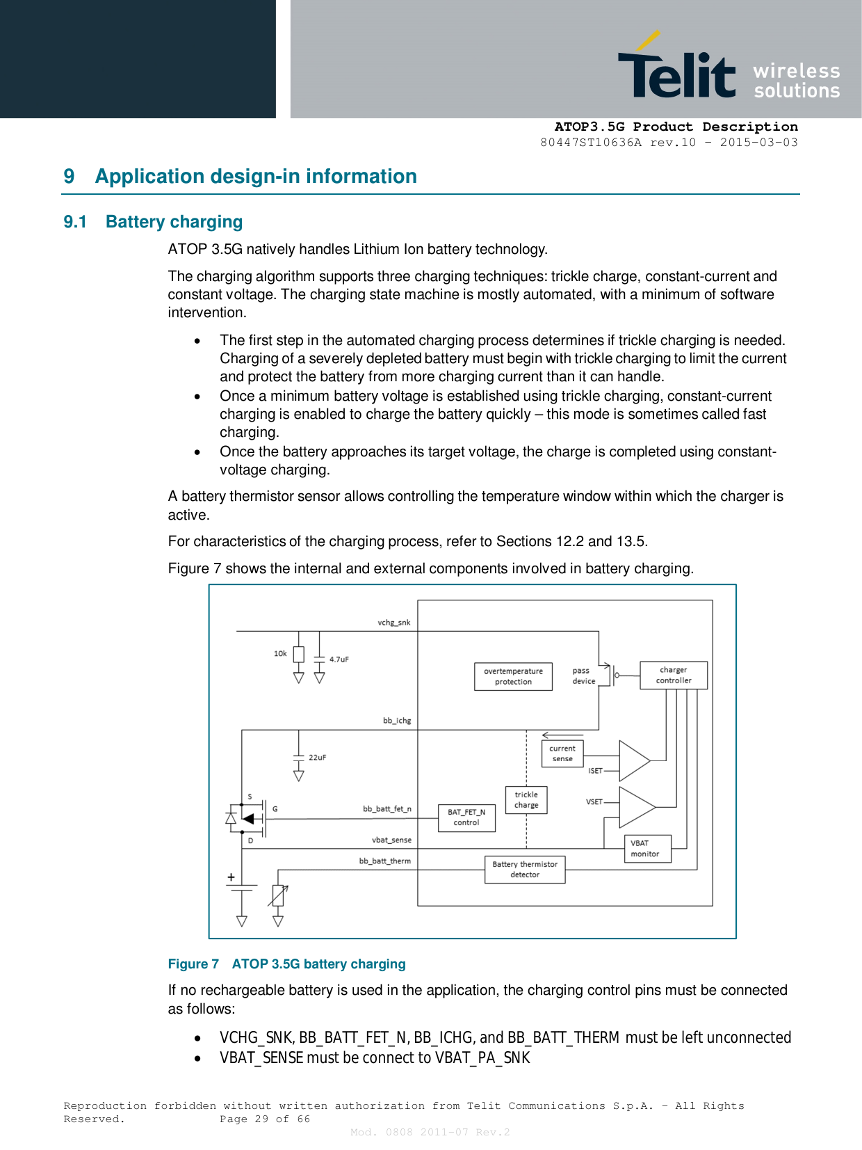
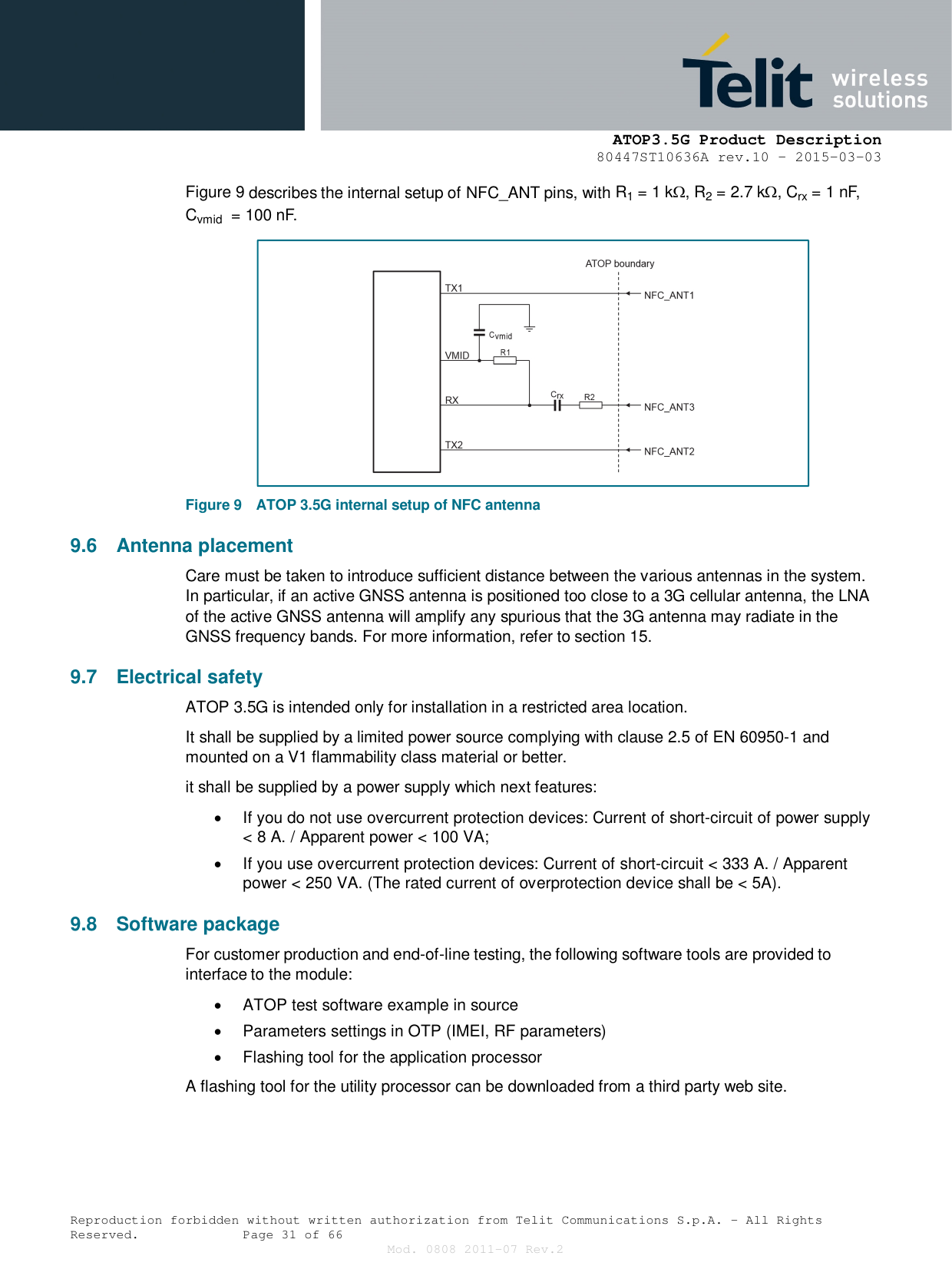
![ATOP3.5G Product Description 80447ST10636A rev.10 – 2015-03-03 Reproduction forbidden without written authorization from Telit Communications S.p.A. - All Rights Reserved. Page 30 of 66 Mod. 0808 2011-07 Rev.2 9.2 Current source ATOP 3.5G handles all its voltage conversion internally. For the Utility Processor, a separate input, VBAT_MC_SNK, is used. Internally, an LDO, controlled by VDD_3V0_SRC_ENA (active HIGH, with internal pull up), converts it to the 3 V required by the utility processor. As described in Figure 8, the output of the LDO is also available externally to power external component, up to a maximum of 50 mA can be drawn, depending on the operating temperature range and the VBAT_MC_SNK value. Other limiting values can be found in Table 14. Figure 8 ATOP 3.5G VDD_3V0_SRC current source 9.3 RTC The MCU RTC is internally supplied by the output of the LDO described in Figure 8. It can also be supplied by a separate battery such as a coin cell via VBAT_RTC_SNK such that the RTC is kept alive in case of power loss. 9.4 ESD protection All pins are tested against ESD according to HBM. Pins that have direct a connection to external world in the application, such as antennas and battery charging, are tested against ESD following HMM models. Human Body Model (HBM): 2000 V requirements are fulfilled Human Metal Model (HMM), detailed list is as follows: o CELL_ANT1 and CELL_ANT2 up to 4 kV o VBAT_SNK, VBAT_MC_SNK, and VBAT_VCC_PA_SNK up to 4 kV o For GPS_PAS _ANT and GPS_ACT_ANT up to 4 kV. For GPS_ACT_ANT an external ESD protection diode is recommended if used externally Charged Device Model (CDM) is considered not applicable for metal-shielded modules, such as OM12030. 9.5 NFC antenna design Remark: This paragraph applies only to OM12030/1X0 (with X as defined in Section 5). For NFC antenna design, refer to Ref [6] for antenna design and Ref [7] in case the application requires to boost the NFC signal.](https://usermanual.wiki/Telit-Communications-S-p-A/OM12030-210/User-Guide-2560823-Page-30.png)
![ATOP3.5G Product Description 80447ST10636A rev.10 – 2015-03-03 Reproduction forbidden without written authorization from Telit Communications S.p.A. - All Rights Reserved. Page 32 of 66 Mod. 0808 2011-07 Rev.2 10 Limiting values Table 5 Power supply Parameters mentioned in this table are indicative and taken from supplier data sheets. Symbol Parameter Conditions Min Max Unit VBAT(VBAT_PA_SNK) battery supply voltage on pin VBAT_PA_SNK battery voltage for RF amplifier 3.2 4.6 V VBAT(VBAT_SNK) battery supply voltage on pin VBAT_SNK battery voltage for application processor 3.2 4.4 V VBAT(VBAT_MC_SNK) battery supply voltage on pin VBAT_MC_SNK battery voltage for utility processor 3.1 5.5 V VBAT(VBAT_RTC_SNK) battery supply voltage on pin VBAT_RTC_SNK battery voltage for utility processor RTC 2.1 3.25 V VBAT(VBAT_CHG) battery supply voltage on pin VBAT_CHG charger supply voltage - 5.0 V VBAT(VBAT_SPKR) battery supply voltage on pin VBAT_SPKR amplifier supply voltage - 5.0 V Table 6 Microcontroller pins Parameters mentioned in this table are indicative and taken from supplier data sheets. Symbol Parameter Conditions Min Max Unit VI(a) analog input voltage on ADC-related pins 0.5 +5.1 V Vi input voltage 5 V tolerant I/O pins [1][2] 0.5 +5.5 V other I/O pins [1] 0.5 +3.6 V input voltage for MC_XTAL1; internal oscillator input 0 1.95 V [1] VBAT(VBAT_MC_SNK) (battery voltage for utility processor) must be present. [2] 3-state outputs go into 3-state mode when VBAT(VBAT_MC_SNK) (battery voltage for utility processor) is grounded. Table 7 Cellular baseband digital interfaces Parameters mentioned in this table are indicative and taken from supplier data sheets. Symbol Parameter Conditions Min Max Unit Vi input voltage 0.5 +2.3 V II input current 100 +100 mA](https://usermanual.wiki/Telit-Communications-S-p-A/OM12030-210/User-Guide-2560823-Page-32.png)
![ATOP3.5G Product Description 80447ST10636A rev.10 – 2015-03-03 Reproduction forbidden without written authorization from Telit Communications S.p.A. - All Rights Reserved. Page 34 of 66 Mod. 0808 2011-07 Rev.2 11 Recommended operating conditions ATOP 3.5G is qualified for automotive use, in accordance with TELIT's "Knowledge-Based Qualification" ("KBQ", based on ZVEI's Robustness Validation, Ref. [1]), using AEC-Q100-defined qualification tests, targeting 15 years lifetime. Table 11 Recommended operating conditions Allowed temperature ranges. Symbol Parameter Conditions Min Max Unit Tstg storage temperature module storage temperature range before final reflow, stored in dry pack 40 +125 °C Tamb ambient temperature module limited ambient temperature range for utility processor (LPC1768) 40 +85 °C module ambient temperature range all functions (the limiting factor is NFC) 30 +85 °C Vch(VCHG_SNK) charge voltage on pin VCHG_SNK - 5.0 V VBAT(VBAT_PA_SNK) battery supply voltage on pin VBAT_PA_SNK battery voltage for RF amplifier 3.4 4.4 V VBAT(VBAT_SNK) battery supply voltage on pin VBAT_SNK battery voltage for application processor 3.2 4.4 V VBAT(VBAT_MC_SNK) battery supply voltage on pin VBAT_MC_SNK battery voltage for utility processor 3.1 5.5 V IBAT(m) peak current to be used to dimension decoupling capacitors on pin VBAT_PA_SNK - 2200 mA 12 Thermal characteristics 12.1 Internal temperature sensor ATOP 3.5G includes an internal temperature sensor. The LPC1768 has access to this sensor to adapt its behavior to conditions. 12.2 Battery charging To improve battery lifetime, it is recommended to avoid charging batteries outside of the temperature range specified by their manufacturers, typically 0 °C to 50 °C.](https://usermanual.wiki/Telit-Communications-S-p-A/OM12030-210/User-Guide-2560823-Page-34.png)
![ATOP3.5G Product Description 80447ST10636A rev.10 – 2015-03-03 Reproduction forbidden without written authorization from Telit Communications S.p.A. - All Rights Reserved. Page 35 of 66 Mod. 0808 2011-07 Rev.2 13 Static characteristics 13.1 Pins Table 12 Characteristics for microcontroller pins Parameters mentioned in this table are indicative and taken from supplier data sheets. Symbol Parameter Conditions Min Typ Max Unit Vo output voltage 0 - 3.0 V VIH HIGH-level input voltage 2.0 - - V VIL LOW-level input voltage - - 0.8 V IIL LOW-level input current VI = 0 V; no pull up - - 10 nA IIH HIGH-level input current VI = 3.0 V; no pull-down - - 10 nA VOH HIGH-level output voltage IOH = 4 mA 2.6 - - V VOL LOW-level output voltage IOL = 4 mA - - 0.4 V IOL LOW-level output current VOL = 0.4 V 4 - - mA IOH HIGH-level output current VOH = 2.6 V 4 - - mA IOSL LOW-level short-circuit output current VI = 3.0 V [1] - - 50 mA IOSH HIGH-level short-circuit output current VI = 0 V [1] - - 45 mA IOZ OFF-state output current VO = 3.0 V or 0 V; no pull up/pull-down - - 10 A Ipd pull-down current VI = 5 V 10 50 150 A Ipu pull up current VI = 0 V 15 50 85 A 3.0 V < VI < 5 V 0 0 0 A Ilu(IO) input/output latch-up current 1.5 V < VI < 4.5 V; Tamb < 125 °C - - 100 mA [1] Only allowed for a short time period. Table 13 Characteristic for baseband digital interface Parameters mentioned in this table are indicative and taken from supplier data sheets. Symbol Parameter Conditions Min Typ Max Unit VIH HIGH-level input voltage 1.2 - 2.1 V VIL LOW-level input voltage 0.3 - 0.6 V IIL LOW-level input current 1 - - A IIH HIGH-level input current - - 1 A VOH HIGH-level output voltage 1.35 - 1.8 V VOL LOW-level output voltage - - 0.1 V Rpu pull up resistance - 100 - kRpd pull-down resistance - 100 - kCi input capacitance - - 10 pF](https://usermanual.wiki/Telit-Communications-S-p-A/OM12030-210/User-Guide-2560823-Page-35.png)
![ATOP3.5G Product Description 80447ST10636A rev.10 – 2015-03-03 Reproduction forbidden without written authorization from Telit Communications S.p.A. - All Rights Reserved. Page 36 of 66 Mod. 0808 2011-07 Rev.2 13.2 Current sources Table 14 VDD_3V0_SRC current source Can be used to supply external components. Symbol Parameter Conditions Min Typ Max Unit Pin: VDD_3V0_SRC Vo output voltage for Tamb = 40 °C to +85 °C 2.9 3.0 3.1 V Io output current - - 50 mA ton turn-on time measured from the moment VDD_3V0_SRC_ENA exceeds 1.4 V [1] - 240 - μs Load regulation ∆VO/(VOx∆IO) relative output voltage variation with output current [1] - 0.002 0.004 %/mA Line regulation ∆VO/(VOx∆VI) relative output voltage variation with input for VBAT(VBAT_MC_SNK) variation [1] 0.1 0.02 0.1 %/V [1] Parameter is indicative and taken from supplier data sheet. Table 15 VSIM_SRC current source To be only used to supply SIM cards[1]. Parameters mentioned in this table are indicative and taken from supplier data sheets. Symbol Parameter Conditions Min Typ Max Unit Pin: VSIM_SRC Vo output voltage for ISO7816-3 class B SIMs 2.80 - 3.00 V for ISO7816-3 class C SIMs 1.7 - 1.80 V Io output current full power mode - - 150 mA sleep mode - - 3 mA [1] Voltage is dynamically controlled to reduce power consumption when SIM card is not accessed.](https://usermanual.wiki/Telit-Communications-S-p-A/OM12030-210/User-Guide-2560823-Page-36.png)
![ATOP3.5G Product Description 80447ST10636A rev.10 – 2015-03-03 Reproduction forbidden without written authorization from Telit Communications S.p.A. - All Rights Reserved. Page 37 of 66 Mod. 0808 2011-07 Rev.2 13.3 Voltage references Table 16 VIO_REF voltage reference To be used as a reference for connecting BB digital interfaces. Parameters mentioned in this table are indicative and taken from supplier data sheets. Symbol Parameter Conditions Min Typ Max Unit Pin: VIO_REF Vo output voltage 1.74 1.80 1.86 V ∆Vo/Vo relative output voltage variation for VBAT (VBAT_SNK) variation - - 3 %/V Table 17 VADC_REF voltage reference Used as power supply reference for internal ADCs. Symbol Parameter Conditions Min Typ Max Unit Pin: VADC_REF Vo output voltage for Tamb = 40 °C to +85 °C 2.9 3.0 3.1 V Io output current for Tamb = 40 °C to +85 °C [1] - - 1 mA ∆Vo/(Vox∆Vi) relative output voltage variation with input voltage for VBAT (VBAT_MC_SNK) variation [2] 0.1 - 0.1 %/V [1] To be used only as a reference voltage. [2] Parameter is indicative and taken from supplier data sheet. 13.4 Clocks Table 18 1PPS This pulse is synchronized with GPS system clock. Symbol Parameter Conditions Min Typ Max Unit tw pulse width - 100 - s tjit jitter time RMS stationary and receiving 4 or more satellites - 4.1 - ms VOH HIGH-level output voltage 1.35 - 1.80 V VOL LOW-level output voltage - - 0.1 V Table 19 BB_EXT_CLK Symbol Parameter Conditions Min Typ Max Unit fxtal reference oscillator frequency - 19.2 - MHz fxtal/fxtal reference oscillator frequency accuracy (40°C to +85°C) - 2 5 ppm VOH HIGH-level output voltage at 6 mA 2.15 2.60 - V VOL LOW-level output voltage at 6 mA - - 0.45 V](https://usermanual.wiki/Telit-Communications-S-p-A/OM12030-210/User-Guide-2560823-Page-37.png)
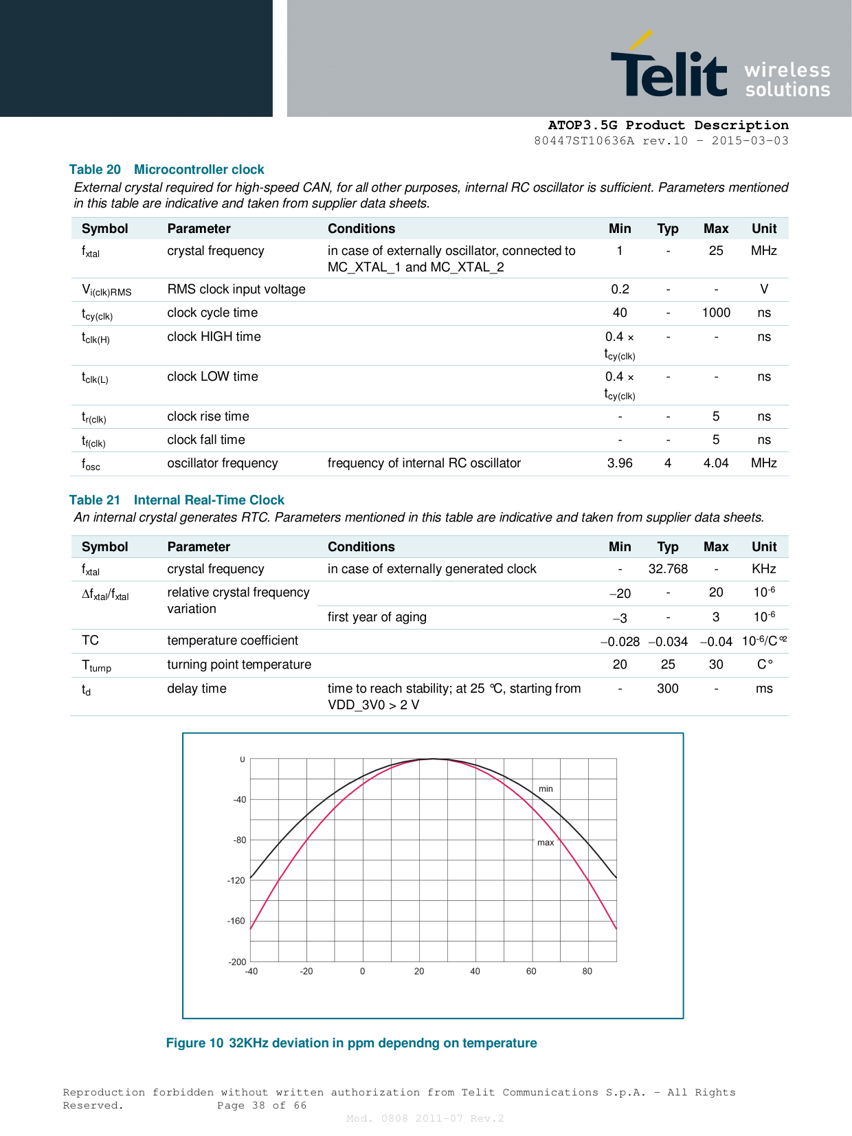
![ATOP3.5G Product Description 80447ST10636A rev.10 – 2015-03-03 Reproduction forbidden without written authorization from Telit Communications S.p.A. - All Rights Reserved. Page 39 of 66 Mod. 0808 2011-07 Rev.2 13.5 Battery charging Table 22 Battery charging Handled by integrated battery charging unit. Parameters mentioned in this table are indicative and taken from supplier data sheets. Symbol Parameter Conditions Min Typ Max Unit VDD(chg) charger supply voltage - - 5 V Ten(ch) charge enable temperature charger only enabled within this window 0 - 40 deg Vch(trickle) trickle charge voltage battery level at which fast charge mode starts - [1] - V Ich(trickle) trickle charge current 10 [1] 160 mA Vch(fast) fast charge voltage constant voltage phase - [1] - V Ich(fast) fast charge current constant current phase IEOC [1] 1000 mA Ieoc end of charge current auto charge ends when battery current reaches this level - [1] Ich(fast) mA Vth(ch) charge threshold voltage auto charge resumes when battery level drops below this level - [1] - V [1] Settings are software programmable, depending on battery technology (LiIon, LiFePO4…) and need to be set accordingly.](https://usermanual.wiki/Telit-Communications-S-p-A/OM12030-210/User-Guide-2560823-Page-39.png)
![ATOP3.5G Product Description 80447ST10636A rev.10 – 2015-03-03 Reproduction forbidden without written authorization from Telit Communications S.p.A. - All Rights Reserved. Page 40 of 66 Mod. 0808 2011-07 Rev.2 14 Dynamic characteristics 14.1 Power consumption Table 23 Utility processor power consumption Measured at Tamb = 25 °C with a power supply at 3.7 V. Covers LPC1768 and LDO. Symbol Parameter Conditions Min Typ Max Unit II input current Cortex M3 at 12 MHz [1] - 7 - mA Cortex M3 at 100 MHz [1] - 45 - mA Cortex M3 in Power-down mode [2] - 100 - A RTC active [3] - 1 - A [1] No peripherals enabled. [2] Wake-up can be initiated by event on RTC, CAN, USB and most GPIOs. [3] In case a separate power source such as a coin cell is connected to VBAT_RTC_SNK and no power is supplied via VBAT_MC_SNK. Table 24 Application processor power consumption Baseband ARM and memories power consumption additionally to cellular function. Symbol Parameter Conditions Min Typ Max Unit II input current application processor - [1] - mA [1] Application dependent. Table 25 Security processor power consumption Measured at Tamb = 25 °C with a power supply at 3.7 V. Only for OM12030/1X0 and OM12030/2X0 (with X as defined in Section 5). Symbol Parameter Conditions Min Typ Max Unit II input current function switched OFF; included in NFC coprocessor - - 0 A function active - 6 - mA Table 26 NFC coprocessor power consumption Measured at Tamb = 25 °C with a power supply at 3.7 V. Covers NFC. Only for OM12030/1X0 (with X as defined in Section 5). Symbol Parameter Conditions Min Typ Max Unit II input current function switched OFF - 2 - A Power-down mode; RF field detection ON - 35 - A NFC and SMX active - 30 - mA NFC and SMX active with RF transmission ongoing - 90 130 mA](https://usermanual.wiki/Telit-Communications-S-p-A/OM12030-210/User-Guide-2560823-Page-40.png)
![ATOP3.5G Product Description 80447ST10636A rev.10 – 2015-03-03 Reproduction forbidden without written authorization from Telit Communications S.p.A. - All Rights Reserved. Page 41 of 66 Mod. 0808 2011-07 Rev.2 Table 27 Communication processor power consumption Measured at Tamb = 25 °C with a power supply at 3.7 V. Symbol Parameter Conditions Min Typ Max Unit DC1800II input current (combined VBAT_SNK and VBAT_PA_SNK) Data transfer WCDMA 2100 (Band I) - 220 630 [2] mA WCDMA 1900 (Band II) - - 630 [2] mA WCDMA 1800 (Band III) - - <tbd> mA WCDMA 1700 (Band IV) - - 630 [2] mA WCDMA 850 (Band V) - - 600 [2] mA WCDMA 900 (Band VIII) - - 600 [2] mA EDGE class 12 (high bands) 4Tx - 1 Rx slots - - 550 [3] mA EDGE class 12 (low bands) - - 600 [3] mA GPRS class 12 (high bands) - - 800 [4] mA GPRS class 12 (low bands) - - 900 [4] mA Voice GSM - - 200 [5] mA WCDMA - - 250 [6] mA Stand-by GSM900 - - 2.3 mA DCS800 - - 2.1 mA WCDMA - - 1.7 mA [1] Average current. Measurements are performed according to 3GPP 4.14 subclause 5.4 for 2G, 34.121 app C2 for 3G. [2] 24 dBm transmit power. [3] 27 dBm for low bands, 26 dBm for high bands. [4] 33 dBm for low bands, 30 dBm for high bands. [5] 33 dBm for low bands, 30 dBm for high bands. [6] Weighted current consumption. Reference document DG.09, WCDMA 2100](https://usermanual.wiki/Telit-Communications-S-p-A/OM12030-210/User-Guide-2560823-Page-41.png)

![ATOP3.5G Product Description 80447ST10636A rev.10 – 2015-03-03 Reproduction forbidden without written authorization from Telit Communications S.p.A. - All Rights Reserved. Page 60 of 66 Mod. 0808 2011-07 Rev.2 21 References [1] ZVEI - Zentralverband Elektrotechnik- und Elektronikindustrie e.V. — http://www.zvei.org/Verband/Publikationen/Seiten/default.aspx?k=robustness%u020validation [2] LPC1768 data sheet — http://www.nxp.com/documents/data_sheet/LPC1769_68_67_66_65_64_63.pdf [3] LPC1768 user manual — http://www.nxp.com/documents/user_manual/UM10360.pdf [4] LPC1768 errata sheet — http://www.nxp.com/documents/errata_sheet/ES_LPC176X.pdf [5] LPC1768 web page —http://www.nxp.com/products/microcontrollers/cortex_m3/lpc1700/LPC1768FET100html#overview [6] AN1445 Antenna design guide for MFRC52x, PN51x, PN53x AN1444 RF Design Guideplus Excel Calculation — http://www.nxp.com/documents/application_note/AN1445_An1444.zip [7] AN1425 RF Amplifier for NFC Reader IC's AN166510 Amplifier antenna matching calculation (Excel) — http://www.nxp.com/documents/application_note/AN1425_AN166510.zip [8] Global Certification Forum — http://www.globalcertificationforum.org [9] R&TTE Radio and Telecommunications Terminal Equipment — http://ec.europa.eu/enterprise/policies/european-standards/harmonised-standards/rtte/ [10] PCS Type Certification Review Board — http://www.ptcrb.org [11] Third-Generation Partnership Project — http://www.3gpp.org [12] Applicable ATOP 3.5G software documentation.](https://usermanual.wiki/Telit-Communications-S-p-A/OM12030-210/User-Guide-2560823-Page-60.png)