Telit Communications S p A UL865NA 2G/3G module User Manual UL865 Hardware User Guide
Telit Communications S.p.A. 2G/3G module UL865 Hardware User Guide
UserManual.wiki
>
Telit Communications S p A
>
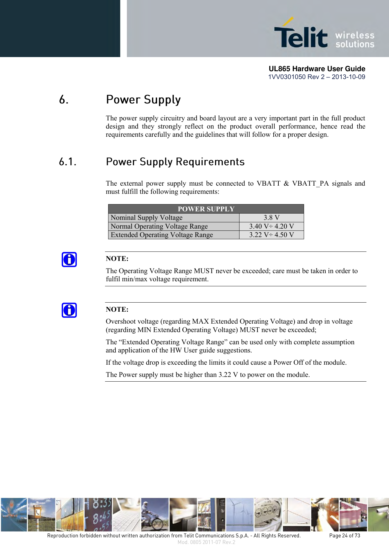
UL865NA User Manual
User guide
Navigation menu
Upload a User Manual
Namespaces
Wiki Guide
HTML
PDF
Info
Views
User Manual
Discussion / Help
Navigation


![UL865 Hardware User Guide 1VV0301050 Rev 2 – 2013-10-09 An AT command is available to use the DAC function. The command is: AT#DAC= [<enable> [, <value>]] <value> - scale factor of the integrated output voltage (0..1023 - 10 bit precision) it must be present if <enable>=1 Refer to SW User Guide or AT Commands Reference Guide for the full description of this function. NOTE: The DAC frequency is selected internally. D/A converter must not be used during POWERSAVING.](https://usermanual.wiki/Telit-Communications-S-p-A/UL865NA/User-Guide-2112049-Page-55.png)
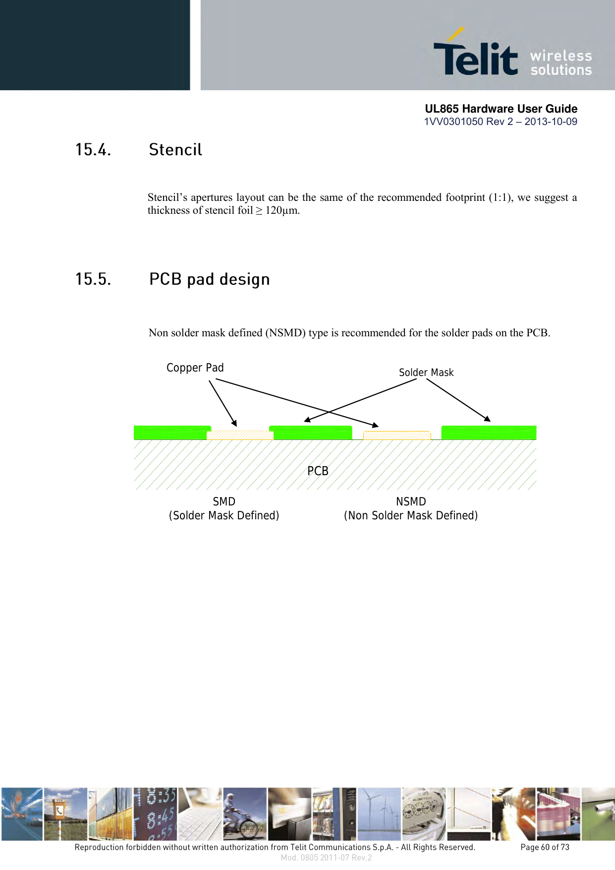

![UL865 Hardware User Guide 1VV0301050 Rev 2 – 2013-10-09 Recommendations for PCB pad surfaces: Finish Layer thickness [µm] Properties Electro-less Ni / Immersion Au 3 –7 / 0.03 – 0.15 good solder ability protection, high shear force values The PCB must be able to resist the higher temperatures which are occurring at the lead-free process. This issue should be discussed with the PCB-supplier. Generally, the wettability of tin-lead solder paste on the described surface plating is better compared to lead-free solder paste. It is not necessary to panel the application PCB, however in that case it is suggested to use milled contours and predrilled board breakouts; scoring or v-cut solutions are not recommended. Lead free Solder paste Sn/Ag/Cu We recommend using only “no clean” solder paste in order to avoid the cleaning of the modules after assembly. Recommended solder reflow profile TL Tsmin Tsmax ts tL tp ttp](https://usermanual.wiki/Telit-Communications-S-p-A/UL865NA/User-Guide-2112049-Page-62.png)