Telit Wireless Solutions BL871 Bluetooth/ BLE HCI Module User Manual BL871E2 HI
Telit Wireless Solutions GmbH Bluetooth/ BLE HCI Module BL871E2 HI
User Manual

BL871E2-HI
Hardware User Guide
1VV0301373 Rev. 2
2017-10-05

BL871E2-HI Hardware User Guide NOTICE
1VV0301373 Rev. 2 Page 2 of 69 2017-10-05
SPECIFICATIONS ARE SUBJECT TO CHANGE WITHOUT NOTICE
NOTICE
While reasonable efforts have been made to ensure the accuracy of this document, Telit
assumes no liability resulting from any inaccuracies or omissions in this document, or from use
of the information obtained herein. The information in this document has been carefully
checked and is believed to be reliable, however no responsibility is assumed for inaccuracies
or omissions. Telit reserves the right to make changes to any products described herein and
reserves the right to revise this document and to make changes from time to time in content
hereof with no obligation to notify any person of revisions or changes. Telit does not assume
any liability arising out of the application or use of any product, software, or circuit described
herein; neither does it convey license under its patent rights or the rights of others.
It is possible that this publication may contain references to, or information about Telit products
(machines and programs), programming, or services that are not announced in your country.
Such references or information must not be construed to mean that Telit intends to announce
such Telit products, programming, or services in your country.
COPYRIGHTS
This manual and the Telit products described herein may be, include or describe copyrighted
Telit material, such as computer programs stored in semiconductor memories or other media.
Laws in the Italy and other countries preserve for Telit and its licensors certain exclusive rights
for copyrighted material, including the exclusive right to copy, reproduce in any form, distribute
and make derivative works of the copyrighted material. Accordingly, any copyrighted material
of Telit and its licensors contained herein or in the Telit products described in this manual may
not be copied, reproduced, distributed, merged or modified in any manner without the express
written permission of Telit. Furthermore, the purchase of Telit products shall not be deemed to
grant either directly or by implication, estoppel, or otherwise, any license under the copyrights,
patents or patent applications of Telit, as arises by operation of law in the sale of a product.
COMPUTER SOFTWARE COPYRIGHTS
The Telit and Third Party supplied Software (SW) products described in this instruction manual
may include copyrighted Telit and other Third Party supplied computer programs stored in
semiconductor memories or other media. Laws in the Italy and other countries preserve for
Telit and other Third Party supplied SW certain exclusive rights for copyrighted computer
programs, including the exclusive right to copy or reproduce in any form the copyrighted
computer program. Accordingly, any copyrighted Telit or other Third Party supplied SW
computer programs contained in the Telit products described in this manual may not be copied
(reverse engineered) or reproduced in any manner without the express written permission of
Telit or the Third Party SW supplier. Furthermore, the purchase of Telit products shall not be
deemed to grant either directly or by implication, estoppel, or otherwise, any license under the
copyrights, patents or patent applications of Telit or other Third Party supplied SW, except for
the normal non-exclusive, royalty-free license to use that arises by operation of law in the sale
of a product.

BL871E2-HI Hardware User Guide NOTICE
1VV0301373 Rev. 2 Page 3 of 69 2017-10-05
USAGE AND DISCLOSURE RESTRICTIONS
I. License Agreements
The software described in this document is the property of Telit and its licensors. It is furnished
by express license agreement only and may be used only in accordance with the terms of such
an agreement.
II. Copyrighted Materials
Software and documentation are copyrighted materials. Making unauthorized copies is
prohibited by law. No part of the software or documentation may be reproduced, transmitted,
transcribed, stored in a retrieval system, or translated into any language or computer language,
in any form or by any means, without prior written permission of Telit
III. High Risk Materials
Components, units, or third-party products used in the product described herein are NOT fault-
tolerant and are NOT designed, manufactured, or intended for use as on-line control equipment
in the following hazardous environments requiring fail-safe controls: the operation of Nuclear
Facilities, Aircraft Navigation or Aircraft Communication Systems, Air Traffic Control, Life
Support, or Weapons Systems (High Risk Activities"). Telit and its supplier(s) specifically
disclaim any expressed or implied warranty of fitness for such High Risk Activities.
IV. Trademarks
TELIT and the Stylized T Logo are registered in the Trademark Office. All other product or
service names are the property of their respective owners.
V. Third Party Rights
The software may include Third Party Right software. In this case you agree to comply with all
terms and conditions imposed on you in respect of such separate software. In addition to Third
Party Terms, the disclaimer of warranty and limitation of liability provisions in this License shall
apply to the Third Party Right software.
TELIT HEREBY DISCLAIMS ANY AND ALL WARRANTIES EXPRESS OR IMPLIED FROM
ANY THIRD PARTIES REGARDING ANY SEPARATE FILES, ANY THIRD PARTY
MATERIALS INCLUDED IN THE SOFTWARE, ANY THIRD PARTY MATERIALS FROM
WHICH THE SOFTWARE IS DERIVED (COLLECTIVELY “OTHER CODE”), AND THE USE
OF ANY OR ALL THE OTHER CODE IN CONNECTION WITH THE SOFTWARE,
INCLUDING (WITHOUT LIMITATION) ANY WARRANTIES OF SATISFACTORY QUALITY
OR FITNESS FOR A PARTICULAR PURPOSE.
NO THIRD PARTY LICENSORS OF OTHER CODE SHALL HAVE ANY LIABILITY FOR ANY
DIRECT, INDIRECT, INCIDENTAL, SPECIAL, EXEMPLARY, OR CONSEQUENTIAL
DAMAGES (INCLUDING WITHOUT LIMITATION LOST PROFITS), HOWEVER CAUSED
AND WHETHER MADE UNDER CONTRACT, TORT OR OTHER LEGAL THEORY, ARISING
IN ANY WAY OUT OF THE USE OR DISTRIBUTION OF THE OTHER CODE OR THE
EXERCISE OF ANY RIGHTS GRANTED UNDER EITHER OR BOTH THIS LICENSE AND
THE LEGAL TERMS APPLICABLE TO ANY SEPARATE FILES, EVEN IF ADVISED OF THE
POSSIBILITY OF SUCH DAMAGES.

BL871E2-HI Hardware User Guide PRODUCT APPLICABILITY TABLE
1VV0301373 Rev. 2 Page 4 of 69 2017-10-05
PRODUCT APPLICABILITY TABLE
Table 0-1 Product Applicability Table
PRODUCT IDS
Product IDs
Regulatory Agency ID
FCC RFR-BL871
IC 23249-BL871
Table 0-1 Product IDs
PRODUCT
BL871E2-HI

BL871E2-HI Hardware User Guide Federal Communication
Commission Interference Statement
1VV0301373 Rev. 2 Page 5 of 69 2017-10-05
FEDERAL COMMUNICATION COMMISSION
INTERFERENCE STATEMENT
This equipment has been tested and found to comply with the limits for a Class B digital device,
pursuant to Part 15 of the FCC Rules. These limits are designed to provide reasonable protection
against harmful interference in a residential installation.
This equipment generates, uses and can radiate radio frequency energy and, if not installed and
used in accordance with the instructions, may cause harmful interference to radio communications.
However, there is no guarantee that interference will not occur in a particular installation. If this
equipment does cause harmful interference to radio or television reception, which can be
determined by turning the equipment off and on, the user is encouraged to try to correct the
interference by one of the following measures:
– Reorient or relocate the receiving antenna.
– Increase the separation between the equipment and receiver.
– Connect the equipment into an outlet on a circuit different from that to which the receiver is
connected.
– Consult the dealer or an experienced radio/TV technician for help.
FCC Caution: Any changes or modifications not expressly approved by the party responsible for
compliance could void the user's authority to operate this equipment.
This device complies with Part 15 of the FCC Rules. Operation is subject to the following two
conditions:
1. This device may not cause harmful interference, and
2. This device must accept any interference received, including interference that may cause
undesired operation.
IMPORTANT NOTE:
FCC Radiation Exposure Statement:
This equipment complies with FCC radiation exposure limits set forth for an uncontrolled
environment. This equipment should be installed and operated with minimum distance 15 mm
between the radiator & your body.
This device is intended only for OEM integrators under the following condition:
- The transmitter module may not be co-located with any other transmitter or antenna,
As long as the condition above is met, further transmitter test will not be required.
However, the OEM integrator is still responsible for testing their end-product for any additional
compliance requirements required with this module installed
IMPORTANT NOTE
In the event that this condition cannot be met (for example certain laptop configurations or co-
location with another transmitter), then the FCC authorization is no longer considered valid and the
FCC ID cannot be used on the final product.
In these circumstances, the OEM integrator will be responsible for re-evaluating the end product
(including the transmitter) and obtaining a separate FCC authorization.
End Product Labeling
The final end product must be labeled in a visible area with the following:
Contains “FCC ID: RMR-BL871”.
Manual Information to the End User
The OEM integrator has to be aware not to provide information to the end user regarding how to
install or remove this RF module in the user’s manual of the end product which integrates this
module. The end user manual shall include all required regulatory information/warning as show in
this manual

BL871E2-HI Hardware User Guide Industry Canada statement
1VV0301373 Rev. 2 Page 6 of 69 2017-10-05
INDUSTRY CANADA STATEMENT
This device complies with Industry Canada licence-exempt RSS standard(s). Operation is
subject to the following two conditions:
1. This device may not cause interference, and
2. This device must accept any interference, including interference that may cause
undesired operation of the device.
Le présent appareil est conforme aux CNR d'Industrie Canada applicables aux appareils radio
exempts de licence. L'exploitation est autorisée aux deux conditions suivantes :
1. l'appareil ne doit pas produire de brouillage, et
2. l'utilisateur de l'appareil doit accepter tout brouillage radioélectrique subi, même si le
brouillage est susceptible d'en compromettre le fonctionnement.
Radiation Exposure Statement:
The product comply with the Canada portable RF exposure limit set forth for an uncontrolled
environment and are safe for intended operation as described in this manual.
The further RF exposure reduction can be achieved if the product can be kept as far as possible
from the user body or set the device to lower output power if such function is available.
Déclaration d'exposition aux radiations:
Le produit est conforme aux limites d'exposition pour les appareils portables RF pour les
Etats-Unis et le Canada établies pour un environnement non contrôlé. Le produit est sûr pour
un fonctionnement tel que décrit dans ce manuel. La réduction aux expositions RF peut être
augmentée si l'appareil peut être conservé aussi loin que possible du corps de l'utilisateur ou
que le dispositif est réglé sur la puissance de sortie la plus faible si une telle fonction est
disponible.
This device is intended only for OEM integrators under the following condition:
- The transmitter module may not be co-located with any other transmitter or antenna.
As long as the condition above is met, further transmitter test will not be required. However,
the OEM integrator is still responsible for testing their end-product for any additional
compliance requirements required with this module installed.
Cet appareil est conçu uniquement pour les intégrateurs OEM dans les conditions suivantes:
- Le module émetteur peut ne pas être coïmplanté avec un autre émetteur ou antenne.
Tant que les 1 condition ci-dessus sont remplies, des essais supplémentaires sur l'émetteur
ne seront pas nécessaires. Toutefois, l'intégrateur OEM est toujours responsable des essais
sur son produit final pour toutes exigences de conformité supplémentaires requis pour ce
module installé.
IMPORTANT NOTE:
In the event that these conditions cannot be met (for example certain laptop configurations or
co-location with another transmitter), then the Canada authorization is no longer considered
valid and the IC ID cannot be used on the final product. In these circumstances, the OEM
integrator will be responsible for re-evaluating the end product (including the transmitter) and
obtaining a separate Canada authorization.
NOTE IMPORTANTE:
Dans le cas où ces conditions ne peuvent être satisfaites (par exemple pour certaines
configurations d'ordinateur portable ou de certaines co-localisation avec un autre émetteur),
l'autorisation du Canada n'est plus considéré comme valide et l'ID IC ne peut pas être utilisé
sur le produit final. Dans ces circonstances, l'intégrateur OEM sera chargé de réévaluer le
produit final (y compris l'émetteur) et l'obtention d'une autorisation distincte au Canada.

BL871E2-HI Hardware User Guide Industry Canada statement
1VV0301373 Rev. 2 Page 7 of 69 2017-10-05
End Product Labeling
The final end product must be labeled in a visible area with the following:
Contains “IC: 4957A-BL871”.
Plaque signalétique du produit final
Le produit final doit être étiqueté dans un endroit visible avec l'inscription suivante:
Contient des “IC: 4957A-BL871".
Manual Information to the End User
The OEM integrator has to be aware not to provide information to the end user regarding how
to install or remove this RF module in the user’s manual of the end product which integrates
this module.
The end user manual shall include all required regulatory information/warning as show in this
manual.
Manuel d'information à l'utilisateur final
L'intégrateur OEM doit être conscient de ne pas fournir des informations à l'utilisateur final
quant à la façon d'installer ou de supprimer ce module RF dans le manuel de l'utilisateur du
produit final qui intègre ce module.
Le manuel de l'utilisateur final doit inclure toutes les informations réglementaires requises et
avertissements comme indiqué dans ce manuel.

BL871E2-HI Hardware User Guide CONTENTS
1VV0301373 Rev. 2 Page 8 of 69 2017-10-05
CONTENTS
NOTICE........................................................................................................... 2
PRODUCT APPLICABILITY TABLE .............................................................. 4
PRODUCT IDS................................................................................................ 4
CONTENTS .................................................................................................... 8
TABLES ........................................................................................................ 11
FIGURES ...................................................................................................... 12
1 INTRODUCTION ............................................................................... 13
1.1 Purpose ....................................................................................... 13
1.2 Audience ..................................................................................... 13
1.3 Contact and Support Information ................................................. 13
1.4 Text Conventions ........................................................................ 14
1.5 Related Documents ..................................................................... 14
1.5.1 Related Documents Requiring a Non-Disclosure Agreement ...... 14
2 PRODUCT DESCRIPTION ................................................................ 15
2.1 Product Overview ........................................................................ 15
2.1.1 Product Features ......................................................................... 15
2.1.2 Applications ................................................................................. 16
2.1.3 Core Chipset ............................................................................... 16
2.1.4 Chip Antenna .............................................................................. 16
2.1.5 Evaluation Kit .............................................................................. 16
2.2 Block Diagram ............................................................................. 17
2.3 Module Photo .............................................................................. 18
3 EVALUATION BOARD (EVB) ........................................................... 19
4 PRODUCT PERFORMANCE ............................................................ 20
4.1 Power and Sensitivity .................................................................. 20
4.2 RF Performance .......................................................................... 20
4.2.1 Bluetooth BR and EDR RF Performance ..................................... 20
4.2.2 Bluetooth Low Energy RF Performance ...................................... 23
4.3 Antenna Radiation Patterns ......................................................... 24
5 HCI INTERFACE ............................................................................... 28
6 ELECTRICAL INTERFACE ............................................................... 29
6.1 Pinout Diagram ........................................................................... 29
6.2 Pinout Table ................................................................................ 30
6.3 DC Power .................................................................................... 31

BL871E2-HI Hardware User Guide CONTENTS
1VV0301373 Rev. 2 Page 9 of 69 2017-10-05
6.3.1 Power Features ........................................................................... 31
6.3.2 Ground ........................................................................................ 31
6.3.3 There are two power supply pins, VBAT and VDDIO. .................. 31
6.3.4 Power Consumption .................................................................... 32
6.3.5 Power and Signal Sequencing .................................................... 33
6.4 Digital Signal Interface Specifications .......................................... 34
6.5 Digital I/O Pins ............................................................................ 35
6.5.1 nSHUTDN (input – active low) ..................................................... 35
6.5.2 SLOW_CLOCK_IN (input) ........................................................... 35
6.5.3 TX_DBG (output) ........................................................................ 35
6.6 UART Interface ........................................................................... 36
6.6.1 UART pinout ............................................................................... 36
6.6.2 Supported interfaces ................................................................... 36
6.6.3 Supported bit rates and format .................................................... 37
6.6.4 RX ............................................................................................... 37
6.6.5 TX ............................................................................................... 37
6.6.6 CTS ............................................................................................. 37
6.6.7 RTS ............................................................................................. 37
6.6.8 UART Timing............................................................................... 38
6.7 PCM Interface ............................................................................. 39
6.7.1 PCM I/O Signals .......................................................................... 39
6.7.2 I2S ............................................................................................... 39
6.7.3 PCM Data Format ....................................................................... 40
6.7.4 PCM Frame-Idle Period ............................................................... 41
6.7.5 PCM Clock Edge Operation ........................................................ 42
6.7.6 PCM Two-Channel Bus Example ................................................ 42
6.7.7 PCM Timing ................................................................................ 43
6.7.8 PCM Assisted Modes .................................................................. 44
7 REFERENCE DESIGN ...................................................................... 50
8 MECHANICAL DRAWINGS .............................................................. 52
8.1 Module Dimensions ..................................................................... 52
8.2 Bottom Side Castellated PAD ...................................................... 52
8.3 Mechanical Outline Drawing ........................................................ 53
9 PCB FOOTPRINT ............................................................................. 54
10 LABELLING & PACKAGING ............................................................ 56
10.1 Module Weight ............................................................................ 56
10.2 Product Labelling ........................................................................ 56
10.3 Packaging ................................................................................... 58
10.3.1 Tray – 450 pcs ........................................................................... 58
10.3.2 Tape & Reel – 1000 pcs .............................................................. 60
11 HANDLING ........................................................................................ 61

BL871E2-HI Hardware User Guide CONTENTS
1VV0301373 Rev. 2 Page 10 of 69 2017-10-05
11.1 Moisture Sensitivity ..................................................................... 61
11.2 ESD Sensitivity ............................................................................ 63
11.3 Reflow ......................................................................................... 63
11.4 Assembly Considerations ............................................................ 63
11.5 Washing Considerations ............................................................. 63
11.6 Safety .......................................................................................... 64
11.7 Disposal ...................................................................................... 64
12 ENVIRONMENTAL REQUIREMENTS .............................................. 65
12.1 Operating Environmental Limits .................................................. 65
12.2 Storage Environmental Limits ...................................................... 65
13 COMPLIANCES ................................................................................ 66
13.1 Bluetooth Qualification ................................................................ 66
13.2 FCC Compliance ......................................................................... 66
13.3 RED Certification ......................................................................... 66
14 SAFETY RECOMMENDATIONS ....................................................... 67
15 DOCUMENT HISTORY ..................................................................... 68

BL871E2-HI Hardware User Guide CONTENTS
1VV0301373 Rev. 2 Page 11 of 69 2017-10-05
TABLES
Table 0-1 Product Applicability Table ................................................................................... 4
Table 0-1 Product IDs............................................................................................................ 4
Table 1-1 Text Symbols ........................................................................................................14
Table 4-1 BT Receiver - In-band Signals ..............................................................................20
Table 4-2 BT Transmitter – GFSK ........................................................................................21
Table 4-3 BT Transmitter – EDR ..........................................................................................21
Table 4-4 BT Modulation – GFSK .........................................................................................22
Table 4-5 BT Modulation – EDR ...........................................................................................22
Table 4-6 Bluetooth LE Receiver - In-band Signals ..............................................................23
Table 4-7 Bluetooth LE Transmitter ......................................................................................23
Table 4-8 Bluetooth LE Modulation .......................................................................................23
Table 6-1 Pinout Table .........................................................................................................30
Table 6-2 VBAT Specifications................................................................................................31
Table 6-3 VBAT Max Ripple ....................................................................................................31
Table 6-4 VDDIO Specifications ..............................................................................................31
Table 6-5 Power Consumption .............................................................................................32
Table 6-6 Input Digital Signal Interface Specifications ..........................................................34
Table 6-7 Output Digital Signal Interface Specifications .......................................................34
Table 6-8 Slow Clock Requirements .....................................................................................35
Table 6-9 UART Timing ........................................................................................................38
Table 6-10 PCM Timing – Master .........................................................................................43
Table 6-11 PCM Timing – Slave ...........................................................................................43
Table 6-12 Assisted HFP - mSBC Parameters .....................................................................44
Table 6-13 Recommended SBC Parameters for Assisted A2DP Mode ................................46
Table 12-1 Operating Environmental Limits ..........................................................................65
Table 12-2 Storage Environmental Limits .............................................................................65
Table 15-1 Document History ...............................................................................................68

BL871E2-HI Hardware User Guide CONTENTS
1VV0301373 Rev. 2 Page 12 of 69 2017-10-05
FIGURES
Figure 2-1 Block Diagram .....................................................................................................17
Figure 2-2 Module Photo .....................................................................................................18
Figure 3-1 Evaluation Board (top) .........................................................................................19
Figure 3-2 Evaluation Board connected to Raspberry Pi (bottom) .......................................19
Figure 4-1XYZ Axis identification ..........................................................................................24
Figure 4-2 Typical Antenna Pattern f = 2400 MHz ................................................................25
Figure 4-3 Typical Antenna Pattern f = 2440 MHz ................................................................26
Figure 4-4 Typical Antenna Pattern f = 2480 MHz ................................................................27
Figure 5-1 Bluetooth Transport Layers .................................................................................28
Figure 6-1 Pinout Diagram ...................................................................................................29
Figure 6-2 Power and Signal Sequencing.............................................................................33
Figure 6-3 H4 (4-wire) UART Interface .................................................................................36
Figure 6-4 H5 (3-wire) UART Interface .................................................................................37
Figure 6-5 UART Timing .......................................................................................................38
Figure 6-6 Frame Idle Period ................................................................................................41
Figure 6-7 Negative Clock Edge Operation ..........................................................................42
Figure 6-8 Two-channel Bus Timing .....................................................................................42
Figure 6-9 PCM Timing ........................................................................................................43
Figure 6-10 Assisted HFP 1.6 - Architecture .........................................................................45
Figure 6-11 Assisted A2DP Sink Architecture .......................................................................48
Figure 6-12 Assisted A2DP Source Architecture ..................................................................49
Figure 7-1 Reference Design - schematic diagram ...............................................................50
Figure 7-2 Reference Design - BOM ....................................................................................51
Figure 8-1 Pad Design (bottom side) ....................................................................................52
Figure 8-2 Mechanical Outline Drawing ................................................................................53
Figure 9-1 Ground Plane and Module Placement .................................................................54
Figure 9-2 PCB Footprint detail - Inner and Bottom Layers ..................................................54
Figure 9-3 PCB Footprint – PCB Top Layer .........................................................................55
Figure 10-1 Product Label ....................................................................................................56
Figure 10-2 Tray Packaging - Tray .......................................................................................58
Figure 10-3 Tray Packaging - Carton ....................................................................................59
Figure 10-4 Tape & Reel Packaging .....................................................................................60
Figure 11-1 Moisture Sensitive Device Label ........................................................................62

BL871E2-HI Hardware User Guide INTRODUCTION
1VV0301373 Rev. 2 Page 13 of 69 2017-10-05
1 INTRODUCTION
1.1 Purpose
The purpose of this document is to provide information regarding the features, functions, and
usage of the BL871E2-HIBluetooth HCI Module with Integrated chip antenna.
1.2 Audience
This document is intended for customer personnel who are responsible for design and
implementation of a Bluetooth product.
1.3 Contact and Support Information
For general contact, technical support services, technical questions, and to report
documentation errors contact Telit Technical Support at:
• ts-srd@telit.com
• TS-EMEA@telit.com
• TS-AMERICAS@telit.com
• TS-APAC@telit.com
Alternatively, use:
• http://www.telit.com/support
For detailed information about where you can buy the Telit modules or for recommendations
on accessories and components visit:
http://www.telit.com
Our aim is to make this guide as helpful as possible. Please keep us informed of your
comments and suggestions for improvements.
Telit appreciates feedback from the users of our information.
BL871E2-HI Hardware User Guide INTRODUCTION
1VV0301373 Rev. 2 Page 14 of 69 2017-10-05
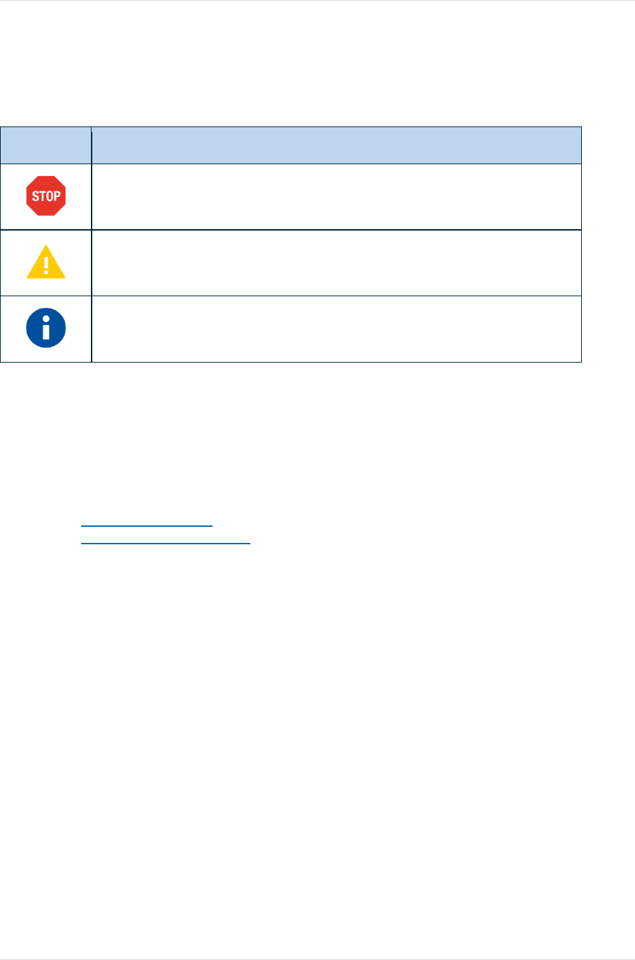
1.4 Text Conventions
Dates are in ISO 8601 format, i.e. YYYY-MM-DD.
Symbol
Description
Danger –
This information MUST be followed or catastrophic
equipment failure and/or bodily injury may occur.
Caution or Warning – This is an important point about integrating the
product into a system. If this information is disregarded, the product or
system may malfunction or fail.
Tip – This is advice or suggestion that may be useful when integrating
the product.
Table 1-1 Text Symbols
1.5 Related Documents
1.5.1 Product Documentation can be found on the web sites:
www.telit.com/gnss
http://www.telit.com/sr-rf/
• BL871E2-HI HCI Module EVK User Guide
1.5.2 Related Documents Requiring a Non-Disclosure Agreement
• None

BL871E2-HI Hardware User Guide PRODUCT DESCRIPTION
1VV0301373 Rev. 2 Page 15 of 69 2017-10-05
2 PRODUCT DESCRIPTION
2.1 Product Overview
The BL871E2-HI is a complete Bluetooth Host Controller Interface (HCI) module.
It supports the following radios:
• Basic Rate (BR)
• Enhanced Data Rate (EDR)
• Low energy (LE)
It is highly optimized for low-cost designs and intended to minimize the customer’s design effort
and time to market. It also features low power consumption (including low power modes).
A chip antenna is included in the module to eliminate RF design tasks.
2.1.1 Product Features
• Complete Bluetooth 4.2 BR/EDR/LE HCI solution with integrated chip antenna
• Best-in-Class Bluetooth (RF) Performance (TX Power, RX Sensitivity, Blocking)
• Very low power consumption, including low power modes of operation
• RED, FCC/IC certification
• Bluetooth BR/EDR
o Up to 7 active devices
o Scatternet: Up to 3 piconets simultaneously, 1 as master and 2 as slaves
o Up to 2 Synchronous Connection Oriented (SCO) links on the same piconet
o Very fast Automatic Frequency Hopping (AFH) algorithm for Asynchronous
Connection-oriented Link (ACL) and eSCO link
o Internal temperature detection and compensation to ensure minimal variation
in RF performance over temperature
o Includes a 128-bit hardware encryption accelerator as defined by the
Bluetooth specifications
o Support for all Voice Air-Coding – Continuously Variable Slope Delta (CVSD),
A-Law, μ-Law, Modified Subband Coding (mSBC), and transparent (uncoded)
o Provides an assisted mode for HFP 1.6 Wideband Speech (WBS) profile or
A2DP profile to reduce host processing workload
o Support of multiple Bluetooth profiles with enhanced QoS
• Bluetooth Low Energy
o Support for up to 10 connections
o Multiple tightly coupled sniff instances to minimize power consumption
o Independent buffering for LE allows large numbers of multiple connections
without affecting BR/EDR performance
o Built-In coexistence and prioritization handling for BR/EDR and LE
• Capabilities of Link Layer Topology Scatternet
• Can act concurrently as peripheral and central
• Time Line Optimization algorithms to achieve maximum channel utilization

BL871E2-HI Hardware User Guide PRODUCT DESCRIPTION
1VV0301373 Rev. 2 Page 16 of 69 2017-10-05
2.1.2 Applications
This ultra-compact BT HCI module is the companion for:
• any 3G/4G Telit cellular product running Telit BT 4.2 BlueCode SR stack
• customers’ MCU running the Telit BT 4.2 BlueCode SR stack
• customer design with its own BT stack driver
• customer design using standard OS (e.g. Android, Windows)
Example applications are:
• Scanner & Printer
• mPOS
• IoT (Healthcare / Industrial Gateway)
2.1.3 Core Chipset
The core chipset for the BL871E2-HI is the TI CC2564C which supports Bluetooth Basic Rate
(BR), Enhanced Data Rate (EDR), and Low Energy (BLE) 4.2.
This HCI device offers best-in-class RF performance with about twice the range of other
Bluetooth LE-only solutions.
Power-management hardware and software algorithms provide significant power savings in all
commonly used Bluetooth BR/EDR/LE modes of operation.
2.1.4 Chip Antenna
The BL871E2-HI includes an Amotech AMAN201510ST01 BT/BLE chip antenna.
2.1.5 Evaluation Kit
An evaluation Kit is available to assist customers in their design, evaluation, and test of the
Bluetooth product. Please see Section 3 EVALUATION board (EVB).
BL871E2-HI Hardware User Guide PRODUCT DESCRIPTION
1VV0301373 Rev. 2 Page 17 of 69 2017-10-05
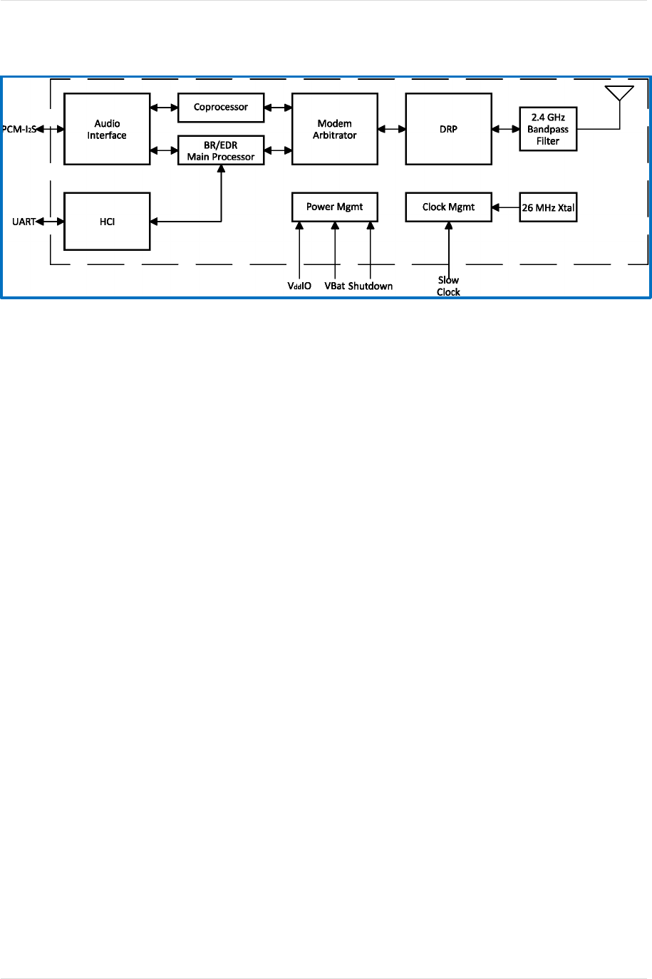
2.2 Block Diagram
Figure 2-1 Block Diagram
BL871E2-HI Hardware User Guide PRODUCT DESCRIPTION
1VV0301373 Rev. 2 Page 18 of 69 2017-10-05
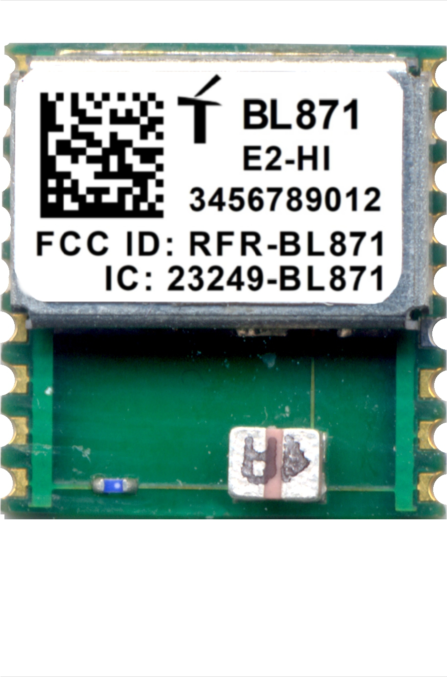
2.3 Module Photo
Figure 2-2 Module Photo
BL871E2-HI Hardware User Guide EVALUATION board (EVB)
1VV0301373 Rev. 2 Page 19 of 69 2017-10-05
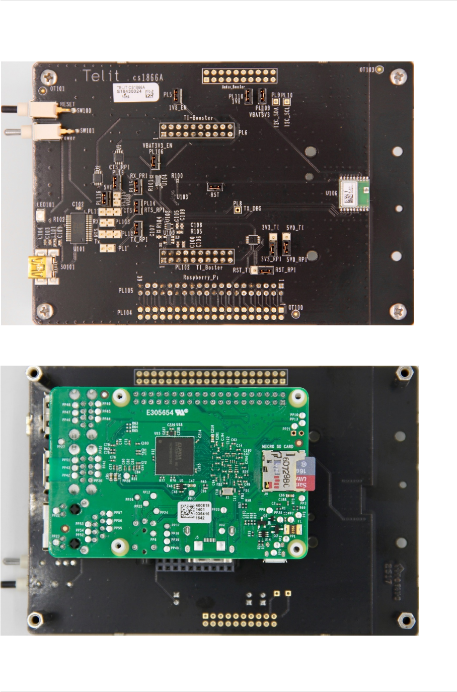
3 EVALUATION BOARD (EVB)
Please refer to the product Evaluation Kit User Guide for detailed information.
Figure 3-1 Evaluation Board (top)
Figure 3-2 Evaluation Board connected to Raspberry Pi (bottom)
BL871E2-HI Hardware User Guide PRODUCT PERFORMANCE
1VV0301373 Rev. 2 Page 20 of 69 2017-10-05
4 PRODUCT PERFORMANCE
4.1 Power and Sensitivity
• Class 1 TX power up to +8 dBm (conducted measurements)
• Receiver Sensitivity: -95 dBm
• Internal temperature detection and compensation to ensure minimal variation in RF
performance over temperature. No external calibration required
• Improved Adaptive Frequency Hopping (AFH) algorithm with minimum adaptation
time
• Longer range, about twice that of other Low-Energy-Only solutions
4.2 RF Performance
Measurements were made with the antenna bypassed with semi-rigid coaxial cable.
4.2.1 Bluetooth BR and EDR RF Performance
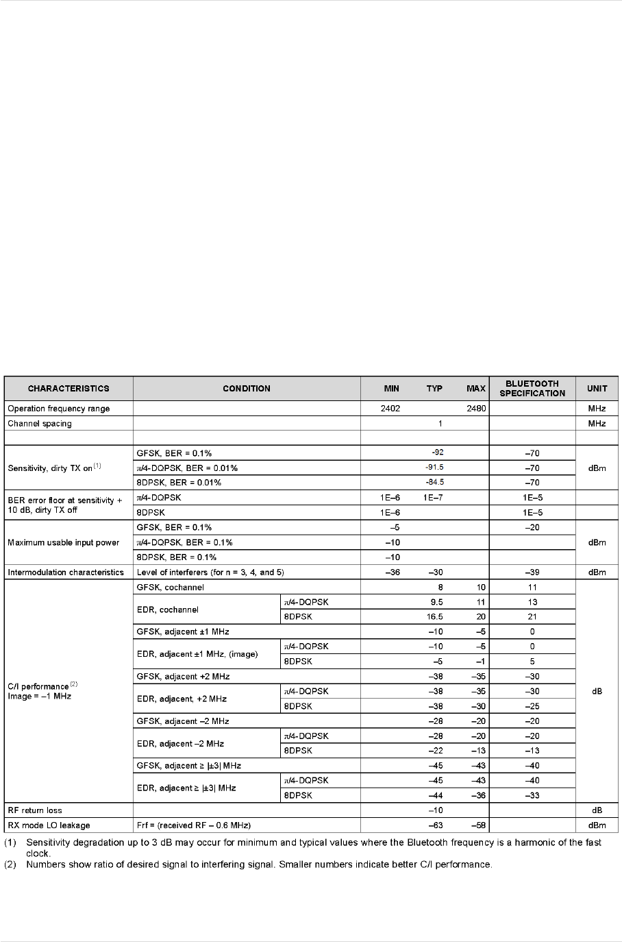
4.2.1.1 Bluetooth Receiver - In-Band Signals
Table 4-1 BT Receiver - In-band Signals
BL871E2-HI Hardware User Guide PRODUCT PERFORMANCE
1VV0301373 Rev. 2 Page 21 of 69 2017-10-05
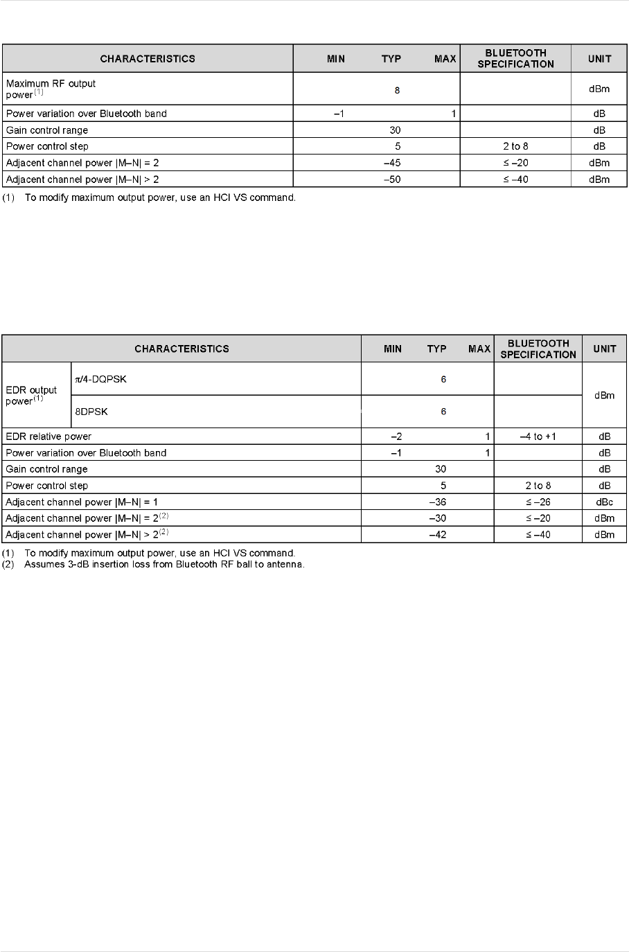
4.2.1.2 Bluetooth Transmitter – GFSK
Table 4-2 BT Transmitter – GFSK
4.2.1.3 Bluetooth Transmitter – EDR
Table 4-3 BT Transmitter – EDR
BL871E2-HI Hardware User Guide PRODUCT PERFORMANCE
1VV0301373 Rev. 2 Page 22 of 69 2017-10-05
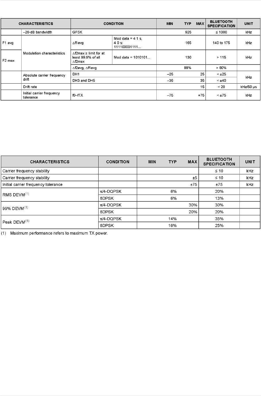
4.2.1.4 Bluetooth Modulation – GFSK
Table 4-4 BT Modulation – GFSK
4.2.1.5 Bluetooth Modulation – EDR
Table 4-5 BT Modulation – EDR
BL871E2-HI Hardware User Guide PRODUCT PERFORMANCE
1VV0301373 Rev. 2 Page 23 of 69 2017-10-05
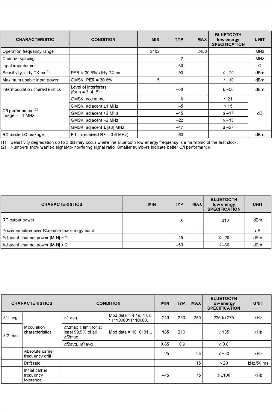
4.2.2 Bluetooth Low Energy RF Performance
4.2.2.1 Bluetooth LE Receiver – In-band Signals
Table 4-6 Bluetooth LE Receiver - In-band Signals
4.2.2.2 Bluetooth LE Transmitter
Table 4-7 Bluetooth LE Transmitter
4.2.2.3 Bluetooth LE Modulation
Table 4-8 Bluetooth LE Modulation
BL871E2-HI Hardware User Guide PRODUCT PERFORMANCE
1VV0301373 Rev. 2 Page 24 of 69 2017-10-05
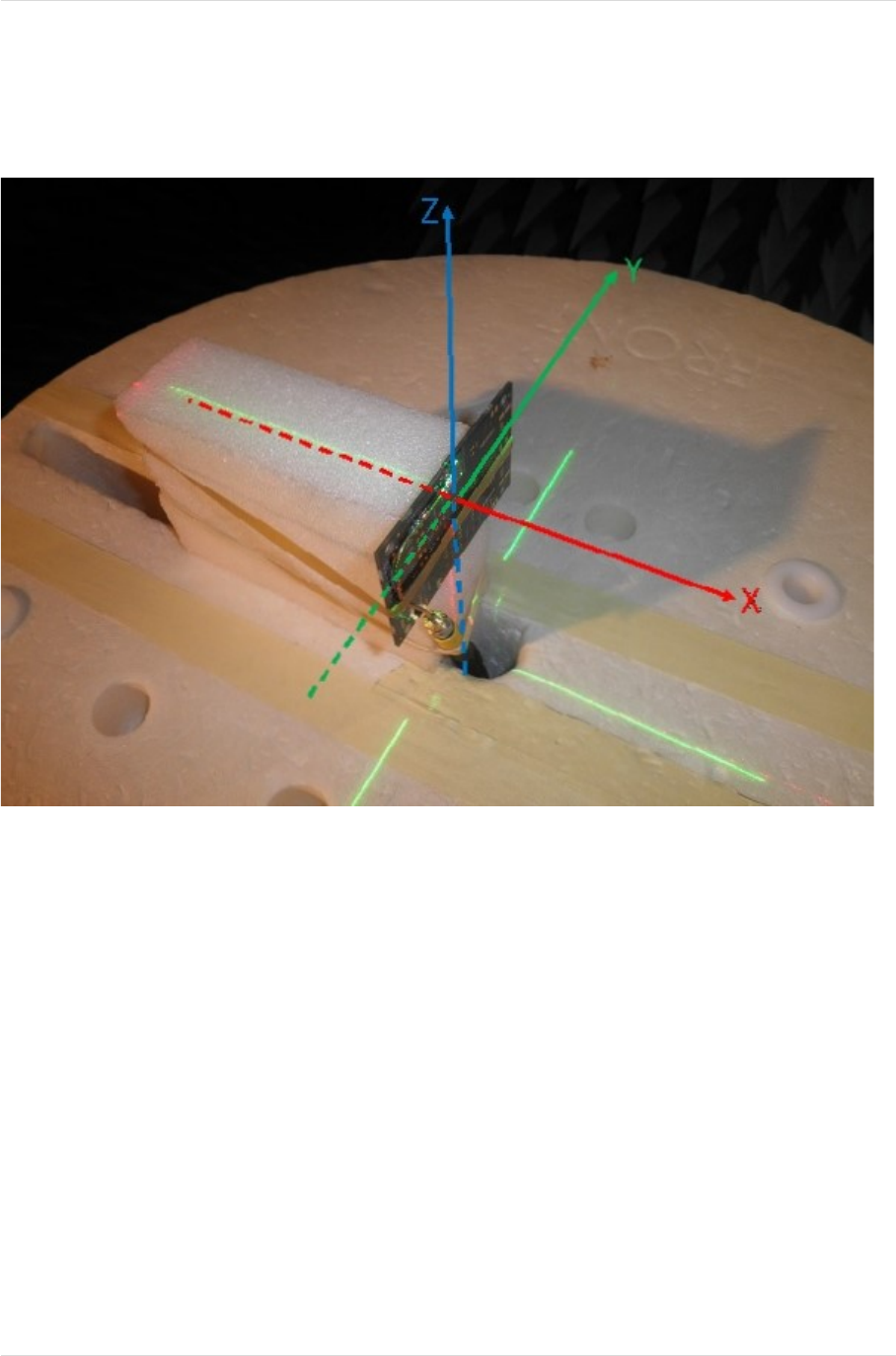
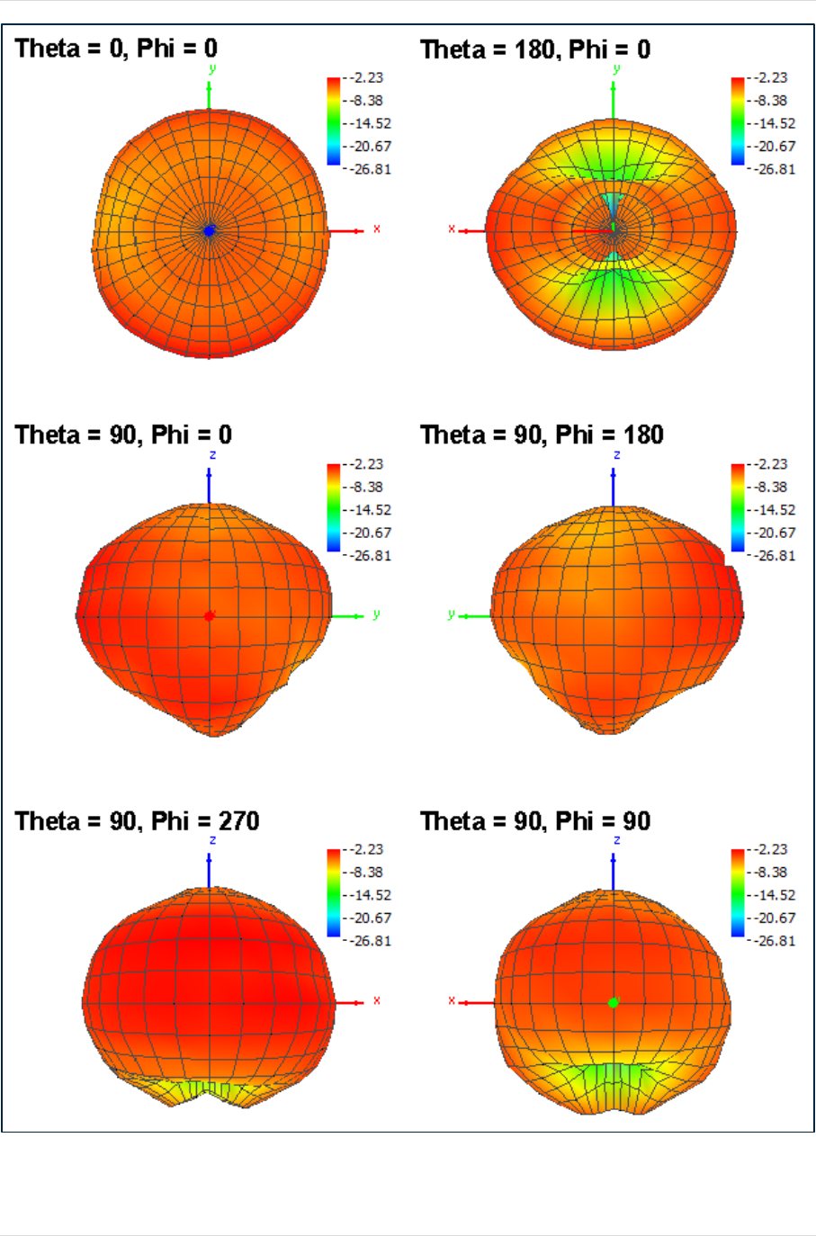
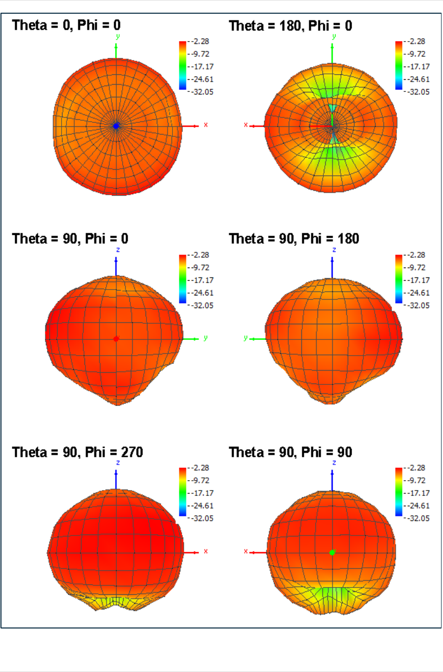
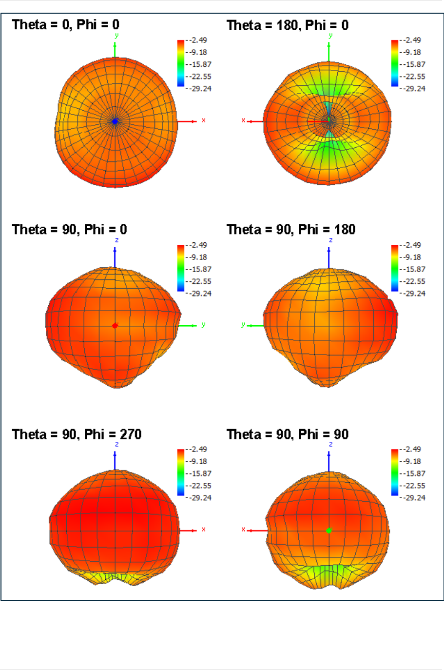
4.3 Antenna Radiation Patterns
The following pages show typical antenna radiation patterns.
The axes are identified below.
Figure 4-1XYZ Axis identification
BL871E2-HI Hardware User Guide PRODUCT PERFORMANCE
1VV0301373 Rev. 2 Page 25 of 69 2017-10-05
Figure 4-2 Typical Antenna Pattern f = 2400 MHz
BL871E2-HI Hardware User Guide PRODUCT PERFORMANCE
1VV0301373 Rev. 2 Page 26 of 69 2017-10-05
Figure 4-3 Typical Antenna Pattern f = 2440 MHz
BL871E2-HI Hardware User Guide PRODUCT PERFORMANCE
1VV0301373 Rev. 2 Page 27 of 69 2017-10-05
Figure 4-4 Typical Antenna Pattern f = 2480 MHz
BL871E2-HI Hardware User Guide HCI INTERFACE
1VV0301373 Rev. 2 Page 28 of 69 2017-10-05
5 HCI INTERFACE
The BL871E2-HI module incorporates a UART interface dedicated to the Host Controller
Interface (HCI) transport layer.
The HCI transports commands, events, and ACL between the device and the host using HCI
data packets.
See Section 6.6 UART Interface for UART interface information.
The Bluetooth transport layers are shown in the following diagram:
Figure 5-1 Bluetooth Transport Layers
Please refer to the Adopted Bluetooth Specifications document for detailed information on the
HCI data protocol.
BL871E2-HI Hardware User Guide ELECTRICAL INTERFACE
1VV0301373 Rev. 2 Page 29 of 69 2017-10-05
6 ELECTRICAL INTERFACE
6.1 Pinout Diagram
Figure 6-1 Pinout Diagram
BL871E2-HI Hardware User Guide ELECTRICAL INTERFACE
1VV0301373 Rev. 2 Page 30 of 69 2017-10-05
6.2 Pinout Table
Pin
Name
Class
Description
1
GND
Ground
Ground. See Section 6.3.2 Ground.
2
GND
Ground
Ground. See Section 6.3.2 Ground.
3
VBAT
Power
Main Supply. See Section 6.3 DC Power.
4
VDDIO
Power
I/O Supply. See Section 6.3 DC Power.
5
PCM_IN
In
PCM. See Section 6.7 PCM Interface.
6
PCM_OUT
Out
PCM. See Section 6.7 PCM Interface.
7
PCM_CLK
I/O
PCM. See Section 6.7 PCM Interface.
8
PCM_FSYNC
I/O
PCM. See Section 6.7 PCM Interface.
9
nSHUTDN
In
Module Control.
See Section 6.5.1 nSHUTDN (input – active low)
10
SLOW_CLK_IN
In
Clock. See Section 6.5.2 SLOW_CLOCK_IN (input)
11
TX_DBG
Out
Debug Messages. See Section 6.5.3 TX_DBG (output)
12
TX
Out
UART Data Output. See Section 06.6 UART Interface.
13
RX
In
UART Data Input. See Section 6.6 UART Interface.
14
CTS
In
UART Flow Control (H4 mode only).
See Section 06.6 UART Interface.
15
RTS
Out
UART Flow Control (H4 mode only).
See Section 6.6 UART Interface.
16
GND
Ground
Ground. See Section 6.3.2 Ground.
17
GND
Ground
Ground. See Section 6.3.2 Ground.
18
GND
Ground
Ground. See Section 6.3.2 Ground.
All GROUND pins must be connected to ground.
Table 6-1 Pinout Table

BL871E2-HI Hardware User Guide ELECTRICAL INTERFACE
1VV0301373 Rev. 2 Page 31 of 69 2017-10-05
6.3 DC Power
6.3.1 Power Features
• Advanced Power Management for extended battery life and ease of design
• On-chip power management, including direct connection to battery
• Low power consumption for Active, Standby, and Scan Bluetooth modes
• Shutdown and Sleep modes to minimize power consumption
6.3.2 Ground
All GROUND pins must be connected to ground.
6.3.3 There are two power supply pins, VBAT and VDDIO.
6.3.3.1 VBAT
Pin
Value
Units
VBAT 2.2 to 4.8 VDC
Table 6-2 VBAT Specifications
VBAT Ripple freq Max Units
0 to 0.1 MHz 60 mV P-P
0.1 to 0.5 Mhz 50 mV P-P
0.5 to 2.5 MHz 30 mV P-P
2.5 to 3.0 MHz 15 mV P-P
> 3.0 MHz
5
mV P-P
Table 6-3 VBAT Max Ripple
6.3.3.2 VDDIO
Pin
Value
Units
V
DDIO 1.62 to 1.92 VDC
Table 6-4 VDDIO Specifications

BL871E2-HI Hardware User Guide ELECTRICAL INTERFACE
1VV0301373 Rev. 2 Page 32 of 69 2017-10-05
6.3.4 Power Consumption
Power-management hardware and firmware algorithms provide significant power savings,
which is a critical parameter in an MCU-based system.
Condition
Typ
Max
Units
Continuous Transmission (EDR) 113 mA
Continuous Transmission (GFSK)
107
mA
Total I/O (active mode) 1 mA
Deep Sleep 40 105 µA
Shutdown 1 7 µA
Table 6-5 Power Consumption
BL871E2-HI Hardware User Guide ELECTRICAL INTERFACE
1VV0301373 Rev. 2 Page 33 of 69 2017-10-05
6.3.5 Power and Signal Sequencing
The following power and signal sequencing is required.
Initial conditions -
VBAT and VDDIO may be on or off.
I/O signal inputs are not allowed if VDDIO is off, except for SLOW_CLK_IN and PCM pins.
1. nSHUTDN must be low.
2. Turn on VBAT. It must be within specification before brining nSHUTDN high.
3. Turn on VDDIO. It must be within specification before brining nSHUTDN high.
4. SLOW_CLOCK_IN must be within specification before brining nSHUTDN high.
5. The module will indicate a successful power up sequence by pulling RTS low.
This may occur up to 100 ms after nSHUTDN goes high.
If RTS does not go low, the module is not properly sequenced up.
Figure 6-2 Power and Signal Sequencing

BL871E2-HI Hardware User Guide ELECTRICAL INTERFACE
1VV0301373 Rev. 2 Page 34 of 69 2017-10-05
6.4 Digital Signal Interface Specifications
Signal
Value
Unit
VIH (min) 0.65 x VDDIO V
VIH (max)
V
DDIO
V
VIL (min) 0 V
VIL (max) 0.35 x VDDIO V
Input impedance 1 MΩ
Input rise & fall times (10% to 90%) 200 (max) ns
Table 6-6 Input Digital Signal Interface Specifications
Signal Value Unit
VOH (min) at 2, 4, 8mA 0.8 x VDDIO V
VOH (min) at 0.1mA VDDIO - 0.2 V
VOH (max) at 2, 4, 8mA VDDIO V
VOL (min)
0
V
VOL (max) at 2, 4, 8mA 0.2 x VDDIO V
VOL (max) at 0.1mA 0.2 V
Output rise & fall times (10% to 90%)
C
L
= 20 pF
10 ns
Table 6-7 Output Digital Signal Interface Specifications
BL871E2-HI Hardware User Guide ELECTRICAL INTERFACE
1VV0301373 Rev. 2 Page 35 of 69 2017-10-05
6.5 Digital I/O Pins
6.5.1 nSHUTDN (input – active low)
nSHUTDN halts operation of the module and performs an internal reset when pulled low.
nSHUTD must be low for a minimum of 5 ms.
The rise time for nSHUTD must not exceed 20 μs.
This pin is pulled low internally through 100 KΩ.
See Section 6.3.5 Power and Signal Sequencing for startup sequencing requirements.
6.5.2 SLOW_CLOCK_IN (input)
The slow clock input as described below must be supplied to operate the module.
The source must be a digital signal in the range of 0 to 1.8 V.
The accuracy of the slow-clock frequency must be 32.768 kHz ±250 ppm for Bluetooth use (as
stated in the Bluetooth specification). The external slow clock must be stable within 64 slow-
clock cycles (2 ms) following the release of nSHUTD.
See Section 6.3.5 Power and Signal Sequencing for startup sequencing requirements
Table 6-8 Slow Clock Requirements
.
6.5.3 TX_DBG (output)
This pin transmits TI internal debugging messages. It is recommended to bring it out to a test
point.
BL871E2-HI Hardware User Guide ELECTRICAL INTERFACE
1VV0301373 Rev. 2 Page 36 of 69 2017-10-05
6.6 UART Interface
A serial data port implements HCI communications into and data out of the BL871-A Module.
The UART implements a single full duplex asynchronous serial port.
Refer to Table 6-6 Input Digital Signal Interface Specifications
for voltage specifications.
6.6.1 UART pinout
TX is the HCI serial output.
RX is the HCI serial input.
RTS is the UART flow control output. (H4 interface only)
CTS is the UART flow control input. (H4 interface only)
6.6.2 Supported interfaces
The UART supports H4 (4-wire) and H5 (3-wire) interfaces:
The interface (H4 vs. H5) is automatically detected upon reception of the first command.
If H4 interface is used, then data flow control signals CTS and RTS are required.
If H5 interface is used, then data flow control is implemented via XON/XOFF.
6.6.2.1 H4 (4-wire) Interface
Figure 6-3 H4 (4-wire) UART Interface
When the UART RX buffer of the module is filled above the flow control threshold, it sets
the RTS signal high to stop transmission from the host.
When the CTS signal is set high, the device stops transmission on the interface. If CTS is
set high while transmitting a byte, the device finishes transmitting the byte and stops the
transmission.
The H4 interface handles the transition between active mode and sleep mode through the
enhanced HCI low level (eHCILL) power-management protocol.
For more information on the H4 UART protocol, see Volume 4 Host Controller Interface,
Part A UART Transport Layer of the Bluetooth Core Specifications
(www.bluetooth.org/en-us/specification/adoptedspecifications).
BL871E2-HI Hardware User Guide ELECTRICAL INTERFACE
1VV0301373 Rev. 2 Page 37 of 69 2017-10-05
6.6.2.2 H5 (3-wire) Interface
Figure 6-4 H5 (3-wire) UART Interface
The H5 protocol supports the following features:
• Software flow control (XON/XOFF)
• Power management using the software messages:
– WAKEUP
– WOKEN
– SLEEP
• CRC data integrity check
For more information on the H5 UART protocol, see Volume 4 Host Controller Interface,
Part D Three- Wire UART Transport Layer of the Bluetooth Core Specifications
(www.bluetooth.org/en-us/specification/adoptedspecifications).
6.6.3 Supported bit rates and format
Data length is 8 bits and 1 stop bit with no parity. The power on default bit rate is 115.2 kbps
Minimum bit rate is 37,500 bps and maximum bit rate is 4 Mbps.
6.6.4 RX
This signal is used to input commands from a host.
In the idle condition, this pin is at logic 1.
6.6.5 TX
This signal is used to output data to the host.
In the idle condition, this pin is at logic 1.
6.6.6 CTS
When the CTS signal is set high by the host, the module stops transmission on the UART
interface.
If CTS is set high while transmitting a byte, the device finishes transmitting the byte and stops
the transmission.
See Figure 6-5 UART Timing.
6.6.7 RTS
When the UART RX buffer of the module passes the flow control threshold, it sets the RTS
signal high to stop transmission from the host.
See Figure 6-5 UART Timing.
BL871E2-HI Hardware User Guide ELECTRICAL INTERFACE
1VV0301373 Rev. 2 Page 38 of 69 2017-10-05
Upon initial power up, RTS will be logic one and then will go to logic zero to indicate a
successful power up sequence.
6.6.8 UART Timing
Figure 6-5 UART Timing
Symbol Description Condition Min Typ Max Units
t1 RTS low to RX data on 0 2 μs
t2 RTS high to RX data off Interrupt = ¼ FIFO 16 byte
t3 CTS low to TX data on 0 2 μs
t4 CTS high to TX data off HW flow control 1 byte
t5 CTS high pulse width 1 bit
Table 6-9 UART Timing

BL871E2-HI Hardware User Guide ELECTRICAL INTERFACE
1VV0301373 Rev. 2 Page 39 of 69 2017-10-05
6.7 PCM Interface
The PCM interface is a fully programmable port to support seamless interfacing with various
PCM and I2S protocols for codec devices.
The interface includes the following features:
• Two voice channels
• Master and slave modes
The module can be either master of the interface (generating Clock and Frame Sync)
or the slave (receiving these two signals).
• All voice coding schemes defined by the Bluetooth specification:
o linear
o Law
o μ-Law
• Long and short frames
• Different data sizes, order, and positions
• High flexibility to support a variety of codecs
• Bus sharing: Data_Out is in the Hi-Z state when the interface is not transmitting voice data.
6.7.1 PCM I/O Signals
6.7.1.1 PCM_IN
This signal is used to input PCM data from a host.
6.7.1.2 PCM_OUT
This signal is used to output PCM data to a host.
6.7.1.3 PCM_CLK
If the PCM interface is in master mode, the module can generate any clock frequency from 64
KHz to 4.096 MHz.
If the PCM interface is in slave mode, clock frequencies up to 15 MHz are supported.
At clock rates above 12 MHz, the maximum data burst size is 32 bits.
6.7.1.4 PCM_FSYNC
If the PCM interface is in master mode, the module generates Frame Sync.
If the PCM interface is in slave mode, the module receives Frame Sync.
6.7.2 I2S
When the codec interface is configured to support the I2S protocol, these settings are recommended:
• Bidirectional, full-duplex interface
• Two time slots per frame: time slot 0 for the left channel audio data; and time slot 1 for the right
channel audio data
• The length of each time slot is configurable up to 40 serial clock cycles, and the length of the frame is
configurable up to 80 serial clock cycles

BL871E2-HI Hardware User Guide ELECTRICAL INTERFACE
1VV0301373 Rev. 2 Page 40 of 69 2017-10-05
6.7.3 PCM Data Format
The data format is fully configurable:
• The data length can be from 8 to 320 bits in 1-bit increments when USING 2 channels,
or up to 640 bits when using 1 channel.
The data length can be set independently for each channel.
• The data position within a frame is also configurable within 1 clock (bit) resolution and can
be set independently (relative to the edge of the Frame_Sync signal) for each
channel.
• The Data_In and Data_Out bit order can be configured independently. For example,
Data_In can start with the most significant bit (MSB);
Data_Out can start with the least significant bit (LSB).
Each channel is separately configurable.
The inverse bit order (LSB first) is supported only for sample sizes up to 24 bits.
• Data_In and Data_Out are not required to be the same length.
• The Data_Out line is configured to Hi-Z output between data words.
Data_Out can also be set for permanent Hi-Z output, regardless of the data output.
This configuration allows the device to be a bus slave in a multislave PCM
environment. At power up, Data_Out is configured as Hi-Z output.
BL871E2-HI Hardware User Guide ELECTRICAL INTERFACE
1VV0301373 Rev. 2 Page 41 of 69 2017-10-05
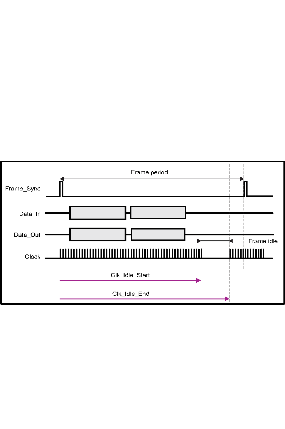
6.7.4 PCM Frame-Idle Period
The codec interface handles frame-idle periods, during which the clock pauses and becomes
0 at the end of the frame after all data are transferred.
The device supports frame-idle periods both as master and slave of the codec bus.
When the device is the master of the interface, the frame-idle period is configurable.
There are two configurable parameters:
• Clk_Idle_Start: indicates the number of clock cycles from the beginning of the frame to the
beginning of the frame-idle period.
After Clk_Idle_Start clock cycles, the clock becomes 0.
• Clk_Idle_End: indicates the time from the beginning of the frame to the end of the
frame-idle period. The time is given in multiples of clock periods.
The delta between Clk_Idle_Start and Clk_Idle_End is the clock idle period.
For example, for clock rate = 1 MHz, frame sync period = 10 kHz, Clk_Idle_Start = 60,
Clk_Idle_End = 90.
Between both Frame_Sync signals there are 70 clock cycles (instead of 100).
The clock idle period starts 60 clock cycles after the beginning of the frame and lasts 90 – 60
= 30 clock cycles. Thus, the idle period ends 100 – 90 = 10 clock cycles before the end of the
frame. The data transmission must end before the beginning of the idle period.
Figure 6-6 Frame Idle Period
BL871E2-HI Hardware User Guide ELECTRICAL INTERFACE
1VV0301373 Rev. 2 Page 42 of 69 2017-10-05
6.7.5 PCM Clock Edge Operation
The codec interface can work on the rising or the falling edge of the clock and can sample
the Frame_Sync signal and the data at inversed polarity.
The operation of a falling-edge-clock type of codec is shown below.
The codec is the master of the bus.
The Frame_Sync signal is updated (by the codec) on the falling edge of the clock and is
therefore sampled (by the device) on the next rising clock.
The data from the codec is sampled (by the device) on the falling edge of the clock.
Figure 6-7 Negative Clock Edge Operation
6.7.6 PCM Two-Channel Bus Example
The figure below shows a 2-channel bus in which the two channels have different word sizes
and arbitrary positions in the bus frame.
Figure 6-8 Two-channel Bus Timing
BL871E2-HI Hardware User Guide ELECTRICAL INTERFACE
1VV0301373 Rev. 2 Page 43 of 69 2017-10-05
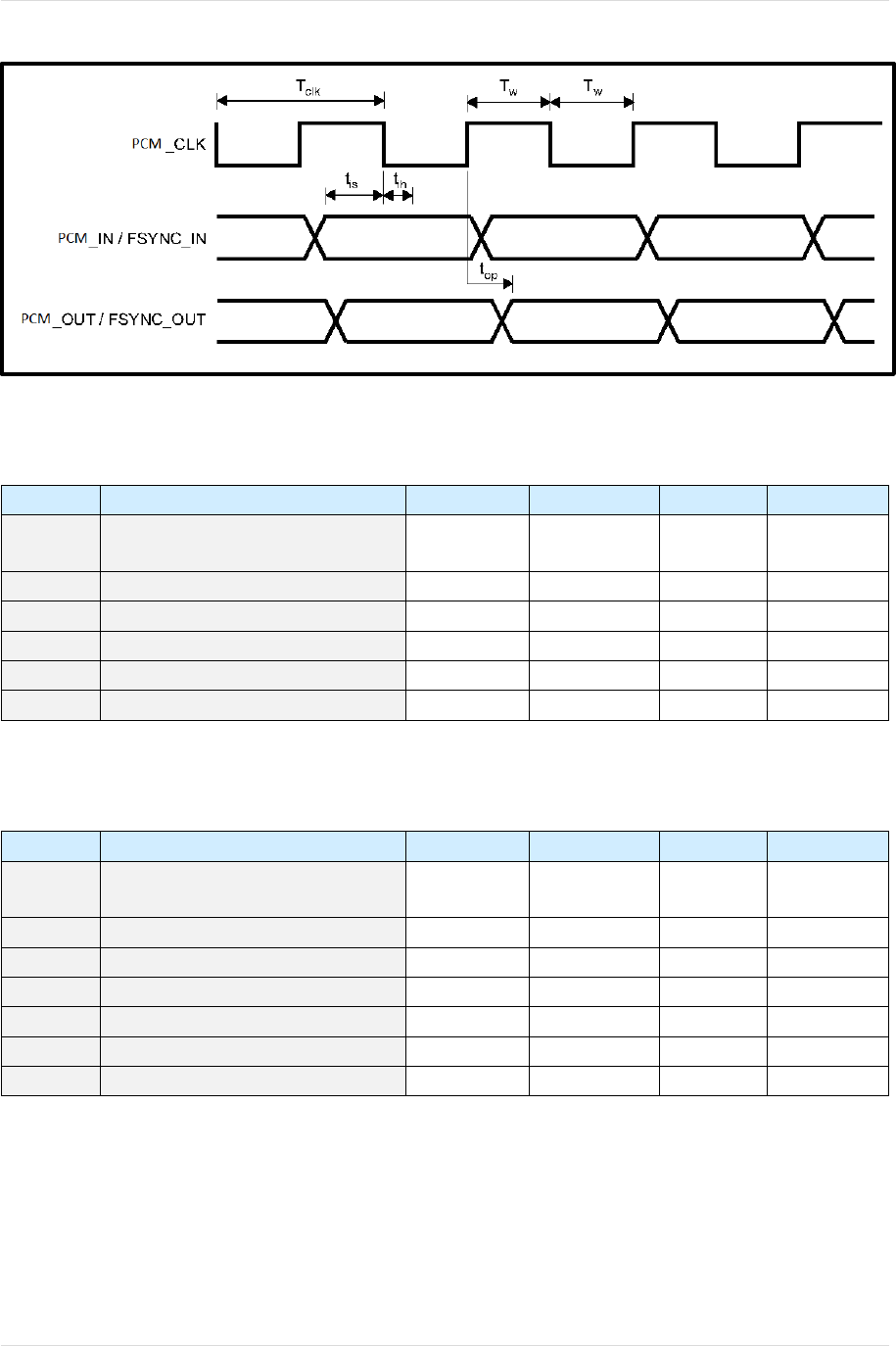
6.7.7 PCM Timing
Figure 6-9 PCM Timing
Symbol
Description
Condition
Min
Max
Unit
t
clk
Cycle time
244.14
4.096 MHz
15625
64 kHz
ns
Tw
Pulse width (hi or lo)
50% of tclk
ns
Tis
PCM_IN setup time
25
ns
Tih
PCM_IN hold time
0
ns
Top
PCM_OUT propagation time
40 pF load
0
10
ns
Top
FSYNC_OUT propagation tm
40 pF load
0
10
ns
Table 6-10 PCM Timing – Master
Symbol
Description
Condition
Min
Max
Unit
t
clk
Cycle time
66.67
15 MHz
ns
Tw
Pulse width (hi or lo)
40% of tclk
ns
Tis
PCM_IN setup time
8
ns
T
ih
PCM_IN hold time
0
ns
Tis
PCM_FSYNC setup time
8
ns
Tih
PCM_FSYNC hold time
0
ns
Top
PCM_OUT Propagation time
40 pF load
0
21
ns
Table 6-11 PCM Timing – Slave

BL871E2-HI Hardware User Guide ELECTRICAL INTERFACE
1VV0301373 Rev. 2 Page 44 of 69 2017-10-05
6.7.8 PCM Assisted Modes
The module contains an embedded coprocessor that can be used for multiple purposes.
It uses a coprocessor to perform the LE functionality or to execute either the assisted HFP 1.6
(WBS) or assisted A2DP functions.
Only one of these functions can be executed at a time because they use the same resources.
The assisted HFP 1.6 (WBS) and assisted A2DP modes of operation comply fully with the
HFP 1.6 and A2DP Bluetooth specifications. For more information on these profiles, see the
corresponding Bluetooth Profile Specification:
www.bluetooth.org/en-us/specification/adopted-specifications
These modes of operation minimize host processing and power by taking advantage of the
device coprocessor to perform the voice and audio SBC processing required in HFP 1.6 (WBS)
and A2DP profiles. This section also compares the architecture of the assisted modes with the
common implementation of the HFP 1.6 and A2DP profiles.
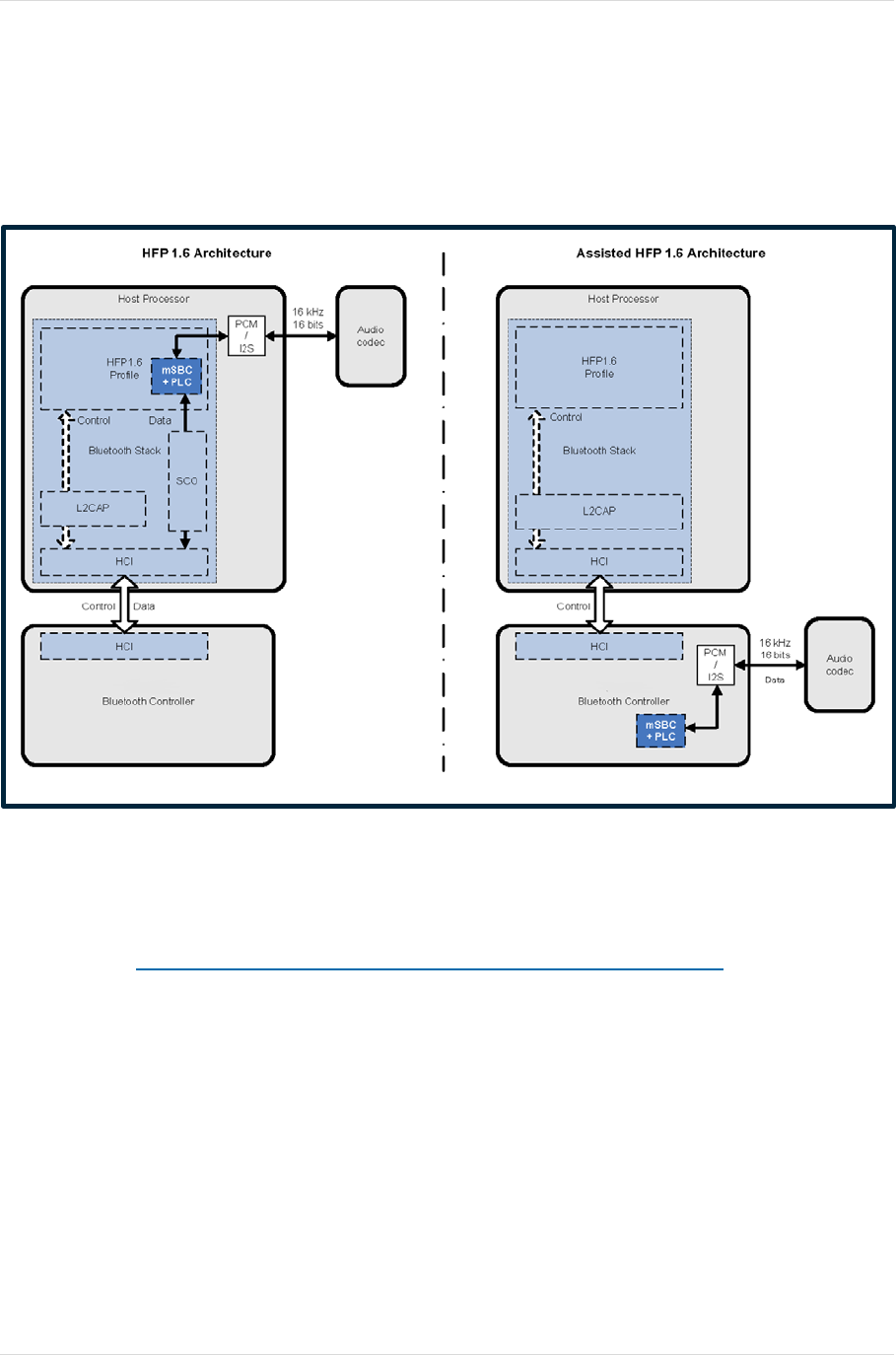
6.7.8.1 Assisted HFP 1.6 (WBS)
The HFP 1.6 Profile Specification adds the requirement for WBS support. The WBS feature
allows twice the voice quality versus legacy voice coding schemes at the same air bandwidth
(64 kbps). This feature is achieved using a voice sampling rate of 16 kHz, a modified subband
coding (mSBC) scheme, and a packet loss concealment (PLC) algorithm. The mSBC scheme
is a modified version of the mandatory audio coding scheme used in the A2DP profile with the
parameters listed below.
Parameter
Value
Channel Mode
Mono
Sampling Rate
16 kHz
Allocation Method
Loudness
Subbands
8
Block Length
15
Bitpool
26
Table 6-12 Assisted HFP - mSBC Parameters
BL871E2-HI Hardware User Guide ELECTRICAL INTERFACE
1VV0301373 Rev. 2 Page 45 of 69 2017-10-05
The assisted HFP 1.6 mode of operation implements this WBS feature on the embedded
CC2564C coprocessor. That is, the mSBC voice coding scheme and the PLC algorithm are
executed in the coprocessor rather than in the host, thus minimizing host processing
workload and power requirements. One WBS connection at a time is supported, and WBS
and NBS connections cannot be used simultaneously in this mode of operation.
The architecture comparison between the common implementation of the HFP 1.6 profile
and the assisted HFP 1.6 solution is shown below.
Figure 6-10 Assisted HFP 1.6 - Architecture
For detailed information on the HFP 1.6 profile, see the Hands-Free Profile 1.6
Specification (www.bluetooth.org/en-us/specification/adopted-specifications).
BL871E2-HI Hardware User Guide ELECTRICAL INTERFACE
1VV0301373 Rev. 2 Page 46 of 69 2017-10-05
6.7.8.2 Assisted A2DP
The advanced audio distribution profile (A2DP) enables wireless transmission of high-quality
mono or stereo audio between two devices. A2DP defines two roles:
• A2DP source is the transmitter of the audio stream.
• A2DP sink is the receiver of the audio stream.
A typical use case streams music from a tablet, phone, or PC (the A2DP source) to
headphones or speakers (the A2DP sink). This section describes the architecture of these
roles and compares them with the corresponding assisted-A2DP architecture. To use the air
bandwidth efficiently, the audio data must be compressed in a proper format. The A2DP
mandates support of the SBC scheme. Other audio coding algorithms can be used; however,
both Bluetooth devices must support the same coding scheme. Since SBC is the only coding
scheme included in all A2DP Bluetooth devices, it is the only coding scheme supported in the
assisted A2DP modes.
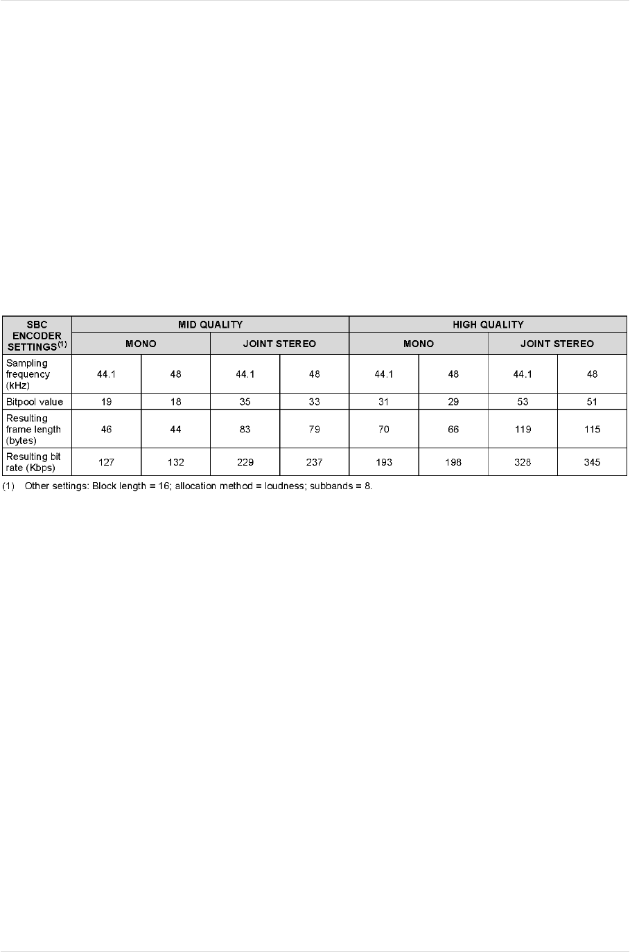
Recommended parameters for the SBC scheme in the assisted A2DP modes are shown
below.
Table 6-13 Recommended SBC Parameters for Assisted A2DP Mode
Supported Channel Modes:
o Mono
o Dual Channel
o Stereo
o Joint Stereo
Supported Sampling Frequencies (kHz):
o 16
o 44.1
o 48
Supported Block Lengths:
o 4
o 8
o 12
o 16
Supported Subbands:
o 4
o 8
Supported Allocation Methods:
o SNR
o Loudness

BL871E2-HI Hardware User Guide ELECTRICAL INTERFACE
1VV0301373 Rev. 2 Page 47 of 69 2017-10-05
Supported Bitpool Ranges:
o Assisted A2DP sink: 2 – 54
o Assisted A2DP source: 2 – 57
Supported L2CAP MTU Sizes (bytes):
o Assisted A2DP sink: 260 – 800
o Assisted A2DP source: 260 – 1021
Miscellaneous Parameters:
o AVDTP Service: Basic type is supported
o L2CAP Basic mode is supported
o L2CAP Flush: Nonflushable is supported
o A2DP content protection: Protected is not supported
BL871E2-HI Hardware User Guide ELECTRICAL INTERFACE
1VV0301373 Rev. 2 Page 48 of 69 2017-10-05
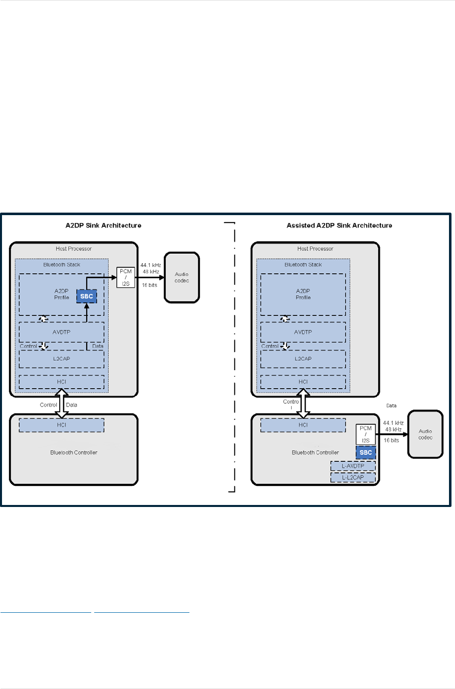
6.7.8.2.1 Assisted A2DP Sink
The role of the A2DP sink is to receive the audio stream in an A2DP Bluetooth connection. In
this role, the A2DP layer and its underlying layers are responsible for link management and
data decoding.
To handle these tasks, two logic transports are defined:
• Control and signaling logic transport
• Data packet logic transport
The assisted A2DP takes advantage of this modularity to handle the data packet logic transport
internally. First, the assisted A2DP implements a light L2CAP layer (L-L2CAP) and light
AVDTP layer (L-AVDTP) to defragment the packets. Then the assisted A2DP performs the
SBC decoding on-chip to deliver raw audio data through the device PCM–I2S interface.
A comparison between a common A2DP sink architecture and the assisted A2DP sink
architecture is shown below.
Figure 6-11 Assisted A2DP Sink Architecture
For more information on the A2DP sink role, see the A2DP Profile Specification at
Adopted Bluetooth Core Specifications.
BL871E2-HI Hardware User Guide ELECTRICAL INTERFACE
1VV0301373 Rev. 2 Page 49 of 69 2017-10-05
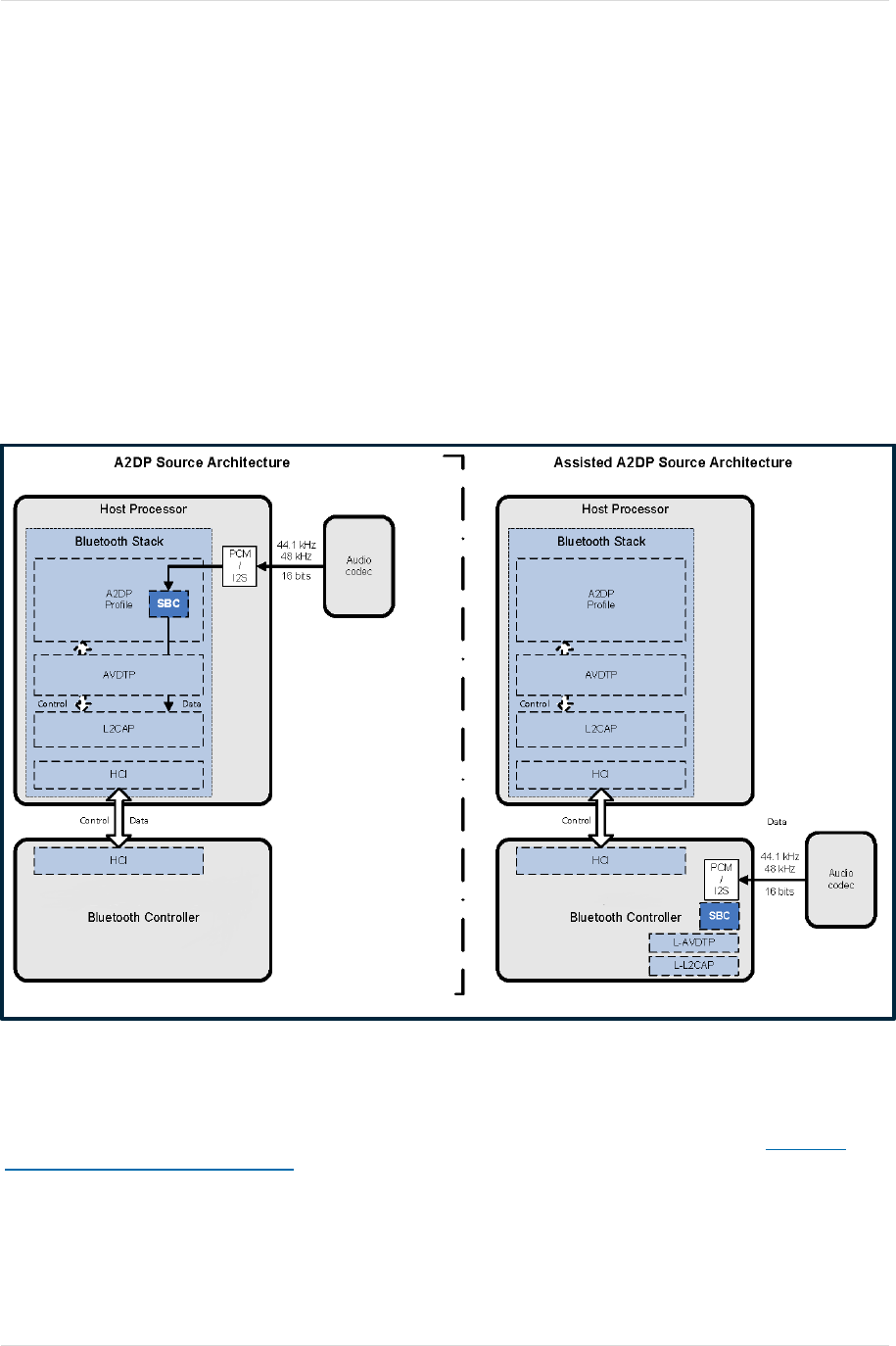
6.7.8.2.2 Assisted A2DP Source
The role of the A2DP source is to transmit the audio stream in an A2DP Bluetooth
connection. In this role, the A2DP layer and its underlying layers are responsible for link
management and data encoding.
To handle these tasks, two logic transports are defined:
• Control and signaling logic transport
• Data packet logic transport
The assisted A2DP takes advantage of this modularity to handle the data packet logic
transport in the device. First, the assisted A2DP encodes the raw data from the PCM–I2S
interface using an on-chip SBC encoder. Then the assisted A2DP implements an L-L2CAP
layer and an L-AVDTP layer to fragment and packetize the encoded audio data.
A comparison between a common A2DP source architecture and the assisted A2DP source
architecture is shown below.
Figure 6-12 Assisted A2DP Source Architecture
For more information on the A2DP source role, see the A2DP Profile Specification at Adopted
Bluetooth Core Specifications.
.
BL871E2-HI Hardware User Guide Reference Design
1VV0301373 Rev. 2 Page 50 of 69 2017-10-05
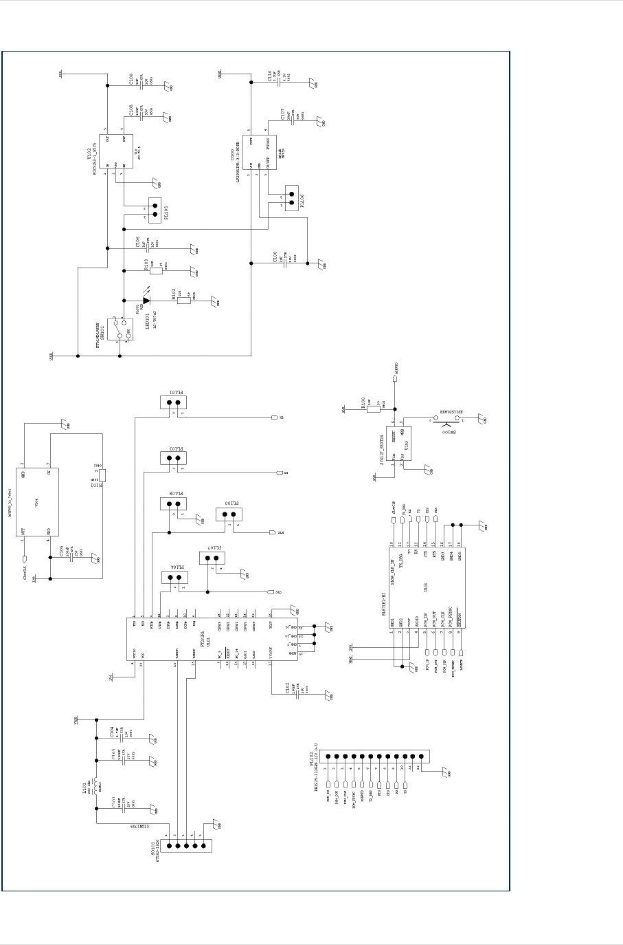
7 REFERENCE DESIGN
Figure 7-1 Reference Design - schematic diagram
BL871E2-HI Hardware User Guide Reference Design
1VV0301373 Rev. 2 Page 51 of 69 2017-10-05
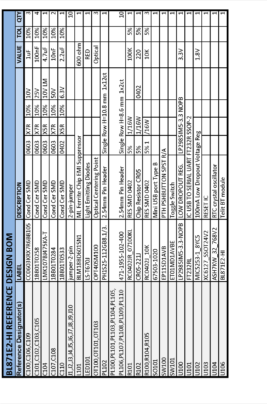
Figure 7-2 Reference Design - BOM
BL871E2-HI Hardware User Guide MECHANICAL DRAWINGS
1VV0301373 Rev. 2 Page 52 of 69 2017-10-05
8 MECHANICAL DRAWINGS
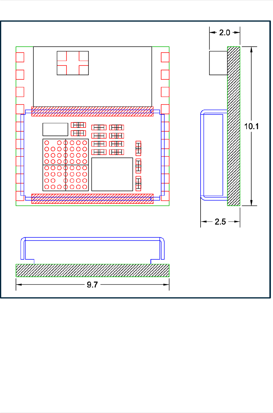
8.1 Module Dimensions
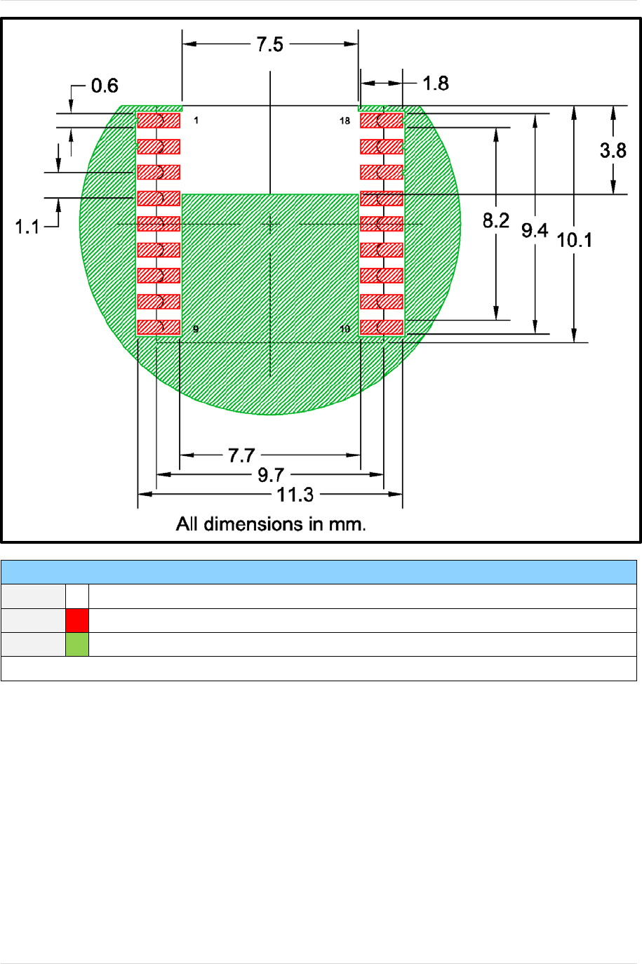
The overall dimensions of the BL871E2-HI are 9.7mm x 10.1mm x 2.5 mm.
The metal shield encompasses only the electronics and not the chip antenna. The maximum
height will be 2.5 mm ± 0.15 mm and is determined by the thickness of the PCB and the shield.
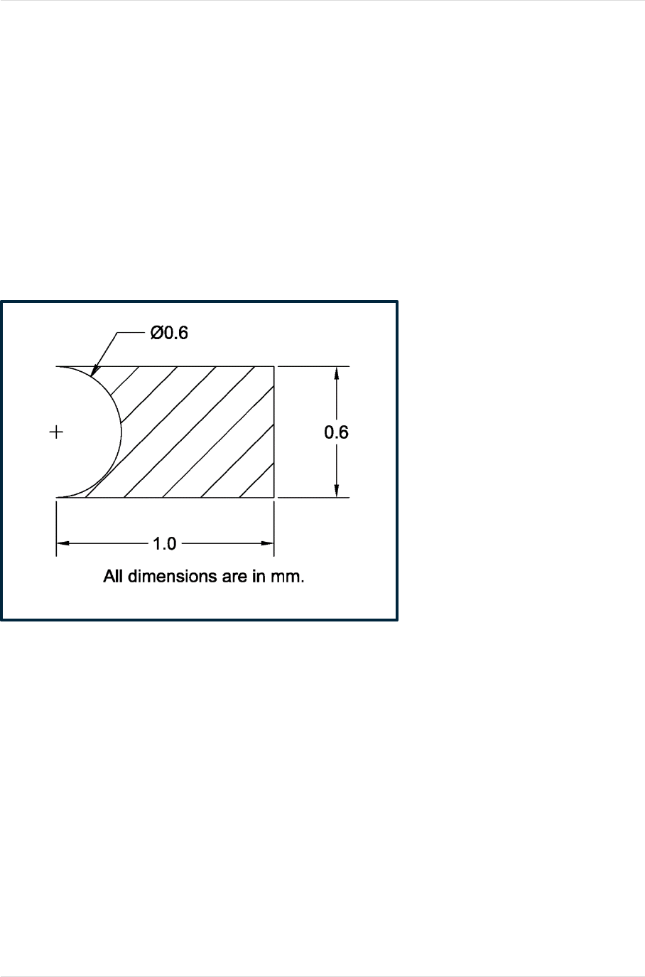
8.2 Bottom Side Castellated PAD
The castellated PAD uses a 0.6mm via with a capture pad of 0.6mm by 1.0mm. During the
board manufacturing process, the pad and the capture pad are routed off at the half way point.
Figure 8-1 Pad Design (bottom side)
BL871E2-HI Hardware User Guide MECHANICAL DRAWINGS
1VV0301373 Rev. 2 Page 53 of 69 2017-10-05
8.3 Mechanical Outline Drawing
Figure 8-2 Mechanical Outline Drawing
BL871E2-HI Hardware User Guide PCB FOOTPRINT
1VV0301373 Rev. 2 Page 54 of 69 2017-10-05
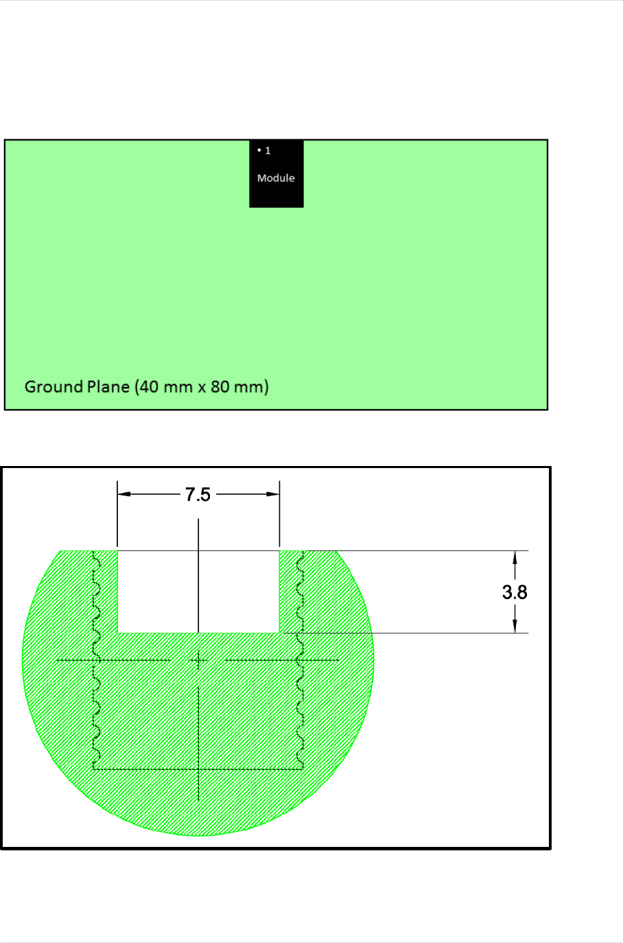
9 PCB FOOTPRINT
The BL871E2-HI requires a ground plane of 40mm by 80mm for the chip antenna to work
properly.
The BL871E2-HI is centered on the long axis of the ground plane. It is placed flush with its top
edge, except for a cutback clearance (determined by the customer’s manufacturing process).
Figure 9-1 Ground Plane and Module Placement
Note: White area shown is a keepout area (no copper or components).
Figure 9-2 PCB Footprint detail - Inner and Bottom Layers
BL871E2-HI Hardware User Guide PCB FOOTPRINT
1VV0301373 Rev. 2 Page 55 of 69 2017-10-05
Figure 9-3 PCB Footprint – PCB Top Layer
Key
White
No copper or components underneath the chip antenna and castellations
Red Module castellations and solder pads
Green Ground plane (partially shown)
Note: This image assumes a clearance of 0.1 mm.
BL871E2-HI Hardware User Guide Labelling & PACKAGING
1VV0301373 Rev. 2 Page 56 of 69 2017-10-05
10 LABELLING & PACKAGING
10.1 Module Weight
The weight of the module is < 0.4 g.
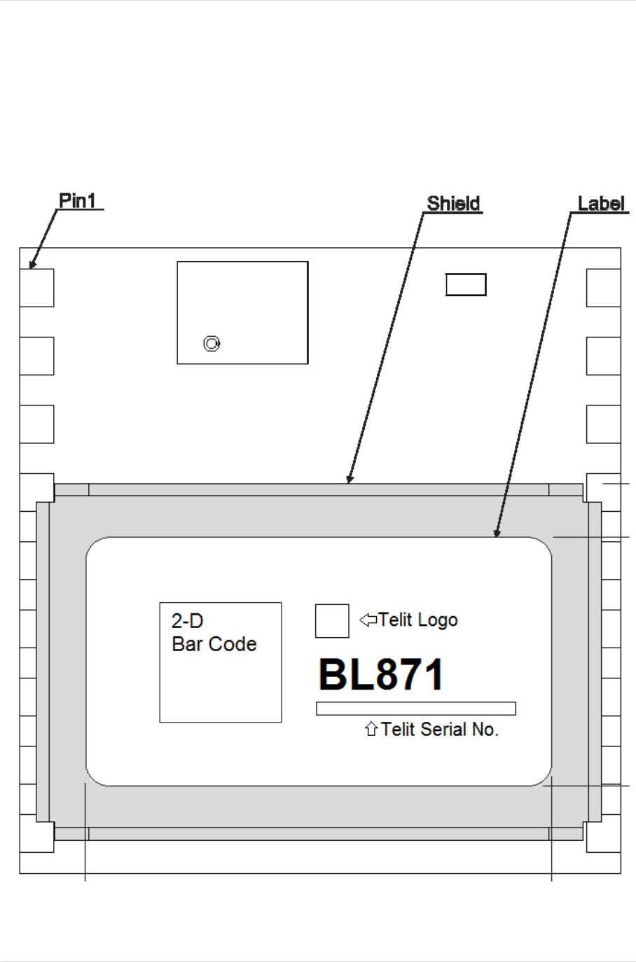
10.2 Product Labelling
Figure 10-1 Product Label
BL871E2-HI Hardware User Guide Labelling & PACKAGING
1VV0301373 Rev. 2 Page 57 of 69 2017-10-05
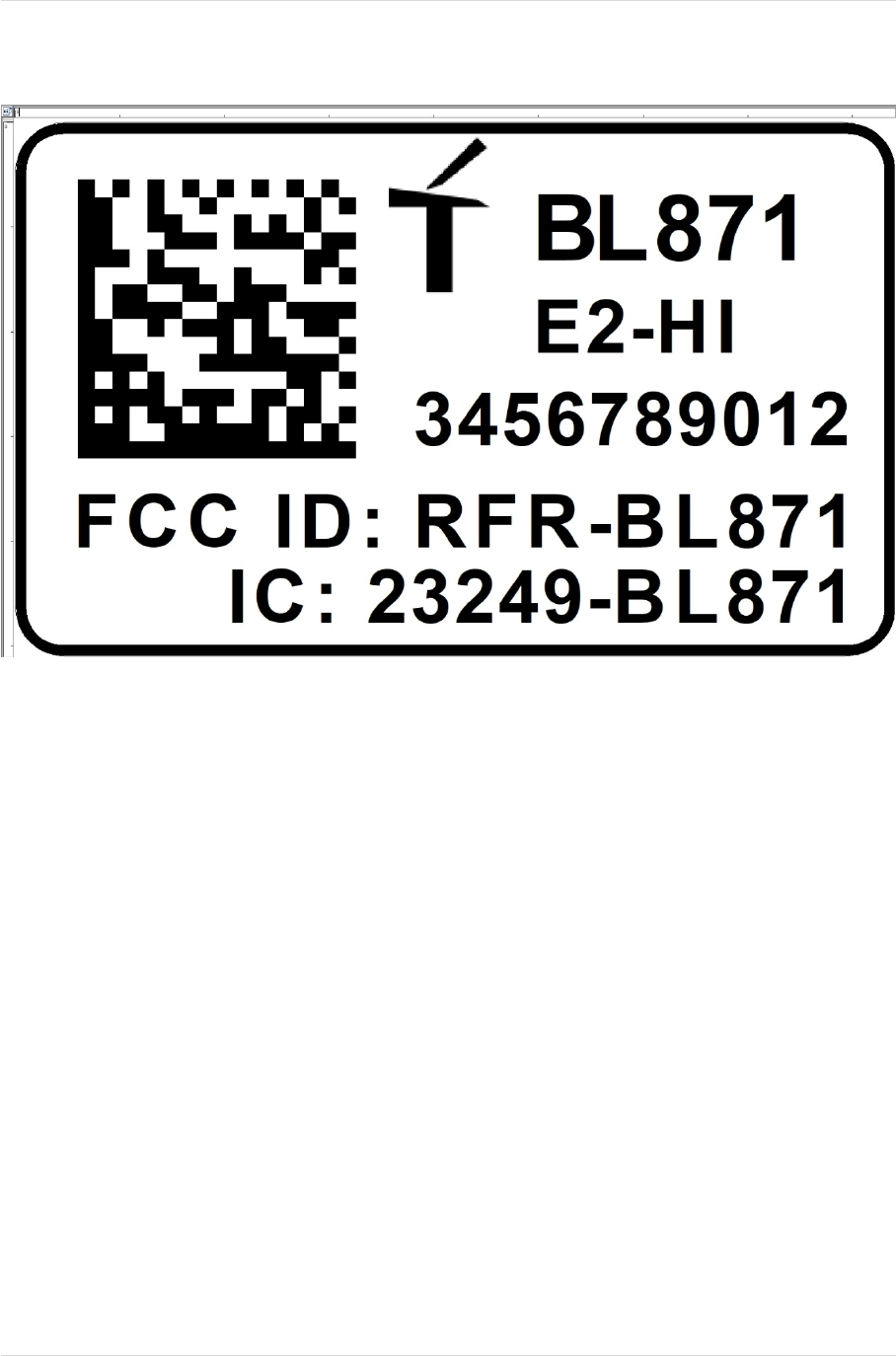
10.3 Label Format
Figure 10-2 Label Layout
BL871E2-HI Hardware User Guide Labelling & PACKAGING
1VV0301373 Rev. 2 Page 58 of 69 2017-10-05
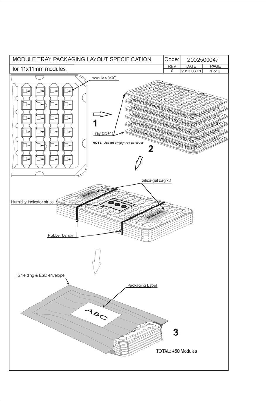
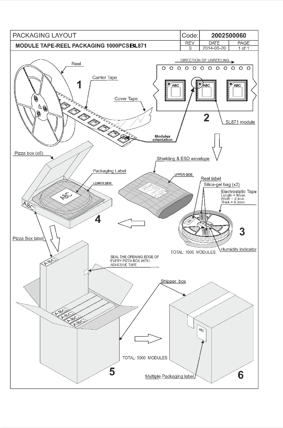
10.4 Packaging
The BL871E2-HI is provided in Tray (450 pcs) and Tape and Reel (1000 pcs) as shown below.
10.4.1 Tray – 450 pcs
Figure 10-3 Tray Packaging - Tray
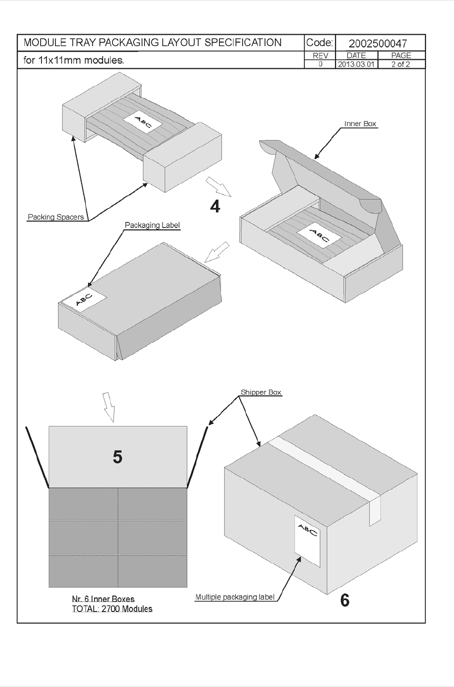
BL871E2-HI Hardware User Guide Labelling & PACKAGING
1VV0301373 Rev. 2 Page 59 of 69 2017-10-05
Figure 10-4 Tray Packaging - Carton
BL871E2-HI Hardware User Guide Labelling & PACKAGING
1VV0301373 Rev. 2 Page 60 of 69 2017-10-05
10.4.2 Tape & Reel – 1000 pcs
Figure 10-5 Tape & Reel Packaging

BL871E2-HI Hardware User Guide HANDLING
1VV0301373 Rev. 2 Page 61 of 69 2017-10-05
11 HANDLING
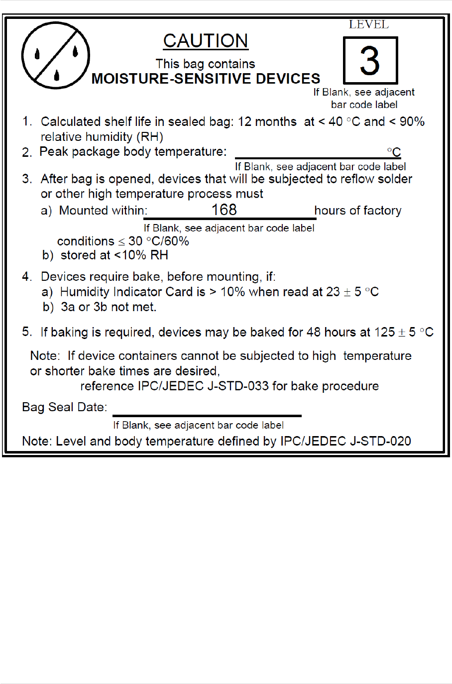
11.1 Moisture Sensitivity
Precautionary measures are required in handling, storing and using these electronic devices
to avoid damage from moisture absorption. If localized heating is required to rework or repair
the device, precautionary methods are required to avoid exposure to solder reflow
temperatures that can result in performance degradation or damage.
The module has a moisture sensitivity level rating of 3 as defined by IPC/JEDEC J-STD-020.
This rating is assigned due to some of the components used within the module.
The modules are supplied in a hermetically sealed bag with desiccant and humidity indicator
cards. The parts must be placed and reflowed within 168 hours of first opening the hermetic
seal provided the factory conditions are less than 30°C and less than 60% and the humidity
indicator card indicates less than 10% relative humidity.
If the package has been opened or the humidity indicator card indicates above 10%, then the
parts will need to be baked prior to reflow. The parts may be baked at +125°C ± 5°C for 48
hours.
However, the packaging materials (tape and reel or trays) can NOT withstand that
temperature. Lower temperature baking is feasible if the humidity level is low and time
is available.
Additional information can be found on the MSL tag affixed to the outside of the hermetically
sealed bag and IPC/JEDEC J-STD-033.
NOTE: JEDEC standards are available free of charge from the JEDEC website
http://www.jedec.org.
BL871E2-HI Hardware User Guide HANDLING
1VV0301373 Rev. 2 Page 62 of 69 2017-10-05
Figure 11-1 Moisture Sensitive Device Label

BL871E2-HI Hardware User Guide HANDLING
1VV0301373 Rev. 2 Page 63 of 69 2017-10-05
11.2 ESD Sensitivity
The module contains class 1 devices and is Electro-Static Discharge Sensitive (ESDS).
Telit recommends the two basic principles of protecting ESD devices from damage:
• Handle sensitive components only in an ESD Protected Area (EPA) under protected
and controlled conditions;
• Protect sensitive devices outside the EPA using ESD protective packaging.
All personnel handling ESDS devices have the responsibility to be aware of the ESD threat to
the reliability of electronic products.
Further information can be obtained from the JEDEC standard JESD625-A Requirements for
Handling Electrostatic Discharge Sensitive (ESDS) Devices.
11.3 Reflow
The modules are compatible with lead free soldering processes as defined in IPC/JEDEC J-
STD-020. The reflow profile must not exceed the profile given IPC/JEDEC J-STD-020 Table
5-2, “Classification Reflow Profiles”.
Although IPC/JEDEC J-STD-020 allows for three reflows, the assembly process for the
module uses one of those profiles, therefore the module is limited to two reflows.
When re-flowing a dual-sided SMT board, it is important to reflow the side containing the
module last. This prevents heavier components within the module from becoming dislodged if
the solder reaches liquidus temperature while the module is inverted.
Note: JEDEC standards are available free from the JEDEC website http://www.jedec.org.
11.4 Assembly Considerations
Since the module contains piezo-electric components, it should be placed near the end of the
assembly process to minimize mechanical shock to it.
During board assembly and singulation process steps, pay careful attention to unwanted
vibrations, resonances and mechanical shocks, e.g. those introduced by manufacturing
equipment.
11.5 Washing Considerations
The module can be washed using standard PCB cleaning procedures after assembly. The
shield does not provide a water-tight seal for the internal components of the module, so it is
important that the module be thoroughly dried prior to use by blowing excess water and then
baking the module to drive out residual moisture. Depending upon the board cleaning
equipment, the drying cycle may not be sufficient to thoroughly dry the module, so additional
steps may need to be taken. Exact process details will need to be determined by the type of
washing equipment as well as other components on the board to which the module is attached.
The module itself can withstand standard JEDEC baking procedures.

BL871E2-HI Hardware User Guide HANDLING
1VV0301373 Rev. 2 Page 64 of 69 2017-10-05
11.6 Safety
Improper handling and use of this module can cause permanent damage to the receiver. There
is also the possible risk of personal injury from mechanical trauma or choking hazard.
Please refer to Section 14 SAFETY RECOMMENDATIONS for further information regarding
safety recommendations.
11.7 Disposal
Telit recommends that this product should not be treated as household waste. For more
detailed information about recycling this product please contact your local waste management
authority or the reseller from whom you purchased the product.

BL871E2-HI Hardware User Guide ENVIRONMENTAL
REQUIREMENTS
1VV0301373 Rev. 2 Page 65 of 69 2017-10-05
12 ENVIRONMENTAL REQUIREMENTS
12.1 Operating Environmental Limits
Temperature
-40°C to +85°C
Temperature Rate of Change
±1°C / minute maximum
Humidity
Up to 95% non-condensing or a wet bulb
temperature of +35°C, whichever is less
Table 12-1 Operating Environmental Limits
12.2 Storage Environmental Limits
Temperature
-40°C to +85°C
Humidity
Up to 95% non-condensing or a wet bulb
temperature of +35°C, whichever is less
Shock (in shipping container)
10 drops from 75 cm onto concrete floor
Table 12-2 Storage Environmental Limits
BL871E2-HI Hardware User Guide COMPLIANCES
1VV0301373 Rev. 2 Page 66 of 69 2017-10-05
13 COMPLIANCES
The modules comply with the following:
• Directive 2011/65/EU art. 16 on the restriction of the use of certain hazardous
substances in electrical and electronic equipment (RoHS)
• Manufactured in an ISO 9001: 2008 accredited facility
• Manufactured to TS 16949:2009 requirements
• Directive 2014/53/EU Radio Equipment Directive (RED)
13.1 Bluetooth Qualification
13.2 FCC Compliance
FCC certification is in progress.
13.3 RED Certification
RED certification is in progress.

BL871E2-HI Hardware User Guide SAFETY RECOMMENDATIONS
1VV0301373 Rev. 2 Page 67 of 69 2017-10-05
14 SAFETY RECOMMENDATIONS
PLEASE READ CAREFULLY
Be sure that the use of this product is allowed in the country and in the environment required.
The use of this product may be dangerous and must be avoided in the following areas:
• Where it can interfere with other electronic devices in environments such as hospitals,
airports, aircraft, etc.
• Where there is risk of explosion such as gasoline stations, oil refineries, etc.
It is the responsibility of the user to enforce the country regulations and specific environmental
regulations.
Do not disassemble the product. Evidence of tampering will invalidate the warranty.
• Telit recommends following the instructions in product user guides for correct
installation of the product.
• The product must be supplied with a stabilized voltage source and all wiring must
conform to security and fire prevention regulations.
• The product must be handled with care, avoiding any contact with the pins because
electrostatic discharges may damage the product itself.
The system integrator is responsible for the functioning of the final product; therefore, care
must be taken with components external to the module, as well as for any project or installation
issue. Should there be any doubt, please refer to the technical documentation and the
regulations in force.
Non-antenna modules must be equipped with a proper antenna with specific characteristics.
The European Community provides some Directives for electronic equipment introduced on
the market. All the relevant information is available on the European Community website:
http://ec.europa.eu/enterprise/sectors/rtte/documents/
The text of the Directive 99/05 regarding telecommunication equipment is available, while the
applicable Directives (Low Voltage and EMC) are available at:
http://ec.europa.eu/enterprise/sectors/electrical/
The power supply used shall comply the clause 2.5 (Limited power sources) of the standard
EN 60950-1 and the module shall be mounted on a PCB which complies with V-0 flammability
class.
Since the module must be built-in to a system, it is intended only for installation in a
RESTRICTED ACCESS LOCATION. Therefore, the system integrator must provide an
enclosure which protects against fire, electrical shock, and mechanical shock in accordance
with relevant standards.

BL871E2-HI Hardware User Guide DOCUMENT HISTORY
1VV0301373 Rev. 2 Page 68 of 69 2017-10-05
15 DOCUMENT HISTORY
Revision
Date
Changes
0
2017-09-08
First Issue
1
2017-10-05
Add FCC and IC IDs
Added FCC and IC regulatory information
Minor text revisions
Table 15-1 Document History

Mod. 0815
2016-08 Rev.1