Telit Wireless Solutions BRSI2 Bluetooth Module User Manual BlueMod P24 P25 Hardware Reference
Stollmann E+V GmbH Bluetooth Module BlueMod P24 P25 Hardware Reference
Contents
- 1. User Manual
- 2. User Manual supplement
User Manual
Stollmann
E + V GmbH
BlueMod+P24 / BlueMod+P25
Hardware reference
BlueMod+P24
BlueMod+P25
Hardware reference
Author: jw Date of Saving: 03.04.06 Ref: BlueMod+P2_HW_reference_V1_5.doc Revision: 1.5 Page 1 of 35

Stollmann
E + V GmbH
BlueMod+P24 / BlueMod+P25
Hardware reference
Note
This device was developed for purposes of communication in an office environment.
It is intended solely for our industrial clients who will physically integrate them into
their own technical products after having them careful examined for their suitability
for the intended purpose by experienced technical personnel. The device was not
developed for or intended for use in any specific customer application. The firmware
of the device may have to be adapted to the specific intended modalities of use or
even replaced by other firmware in order to ensure flawless function in the
respective field of applications. Performance data (range, power requirements, etc.)
may depend on the operating environment, the field of application, the configuration,
and method of control as well as other conditions of use; they may deviate from the
technical specifications, the Design Guide specifications or other product
documentation. The exact performance characteristics can be determined only by
measurements subsequent to integration. Variations in the performance data of
mass-produced devices may occur due to individual differences between such
devices. Device samples were tested in a reference environment for compliance
with the legal requirements applicable to the reference environment. No
representation is made regarding the compliance with legal, regulatory, or other
requirements in other environments. No representation can be made and no
warranty can be assumed regarding the suitability of the device for a specific
purpose as defined by our customers. Stollmann reserves the right to make changes
to the hardware or firmware or to the specifications without prior notice or to replace
the device with a successor model. Of course, any changes to the hardware or
firmware of any devices for which we have entered into a supply agreement with our
customers will be made only if, and only to the extent that, such changes can
reasonably be expected to be acceptable to our customers. No general commitment
will be made regarding periods of availability; these must be subject to individual
agreement. All agreements are subject to our Terms and Conditions for Deliveries
and Payments which you can request from us at any time.
Copyright © 2005-2006 Stollmann E+V GmbH
Trademarks
The Bluetooth® word mark and logos are owned by the Bluetooth SIG, Inc. and any
use of such marks by Stollmann E+V GmbH is under license. Other trademarks and
trade names are those of their respective owners.
Author: jw Date of Saving: 03.04.06 Ref: BlueMod+P2_HW_reference_V1_5.doc Revision: 1.5 Page 2 of 35

Stollmann
E + V GmbH
BlueMod+P24 / BlueMod+P25
Hardware reference
TABLE OF CONTENTS
1 Key Features ...................................................................................................... 6
2 Applications for the Modules............................................................................... 6
3 Description of the Modules ................................................................................. 6
4 Scope of this Document...................................................................................... 7
5 Terminal Layout .................................................................................................. 7
5.1 General Pin Assignment .............................................................................. 8
5.2 Application specific pin multiplexing ............................................................ 9
5.2.1 SPP configuration................................................................................. 9
5.2.2 AudioGateway/Headset – SPP configuration ..................................... 10
6 Block Diagram................................................................................................... 12
7 Terminal Specifics............................................................................................. 12
7.1 Power supply ............................................................................................. 12
7.2 RF-ANTENNA............................................................................................ 12
7.2.1 Typical Radiation Pattern ................................................................... 13
7.2.2 BlueMod+P25..................................................................................... 13
7.3 Reset ......................................................................................................... 13
7.4 UART Interface – TXD, RXD, CTS, RTS................................................... 13
7.5 USB Interface ............................................................................................ 14
7.5.1 D+, D- ................................................................................................. 14
7.5.2 USB Pull-Up Resistor ......................................................................... 14
7.5.3 USB Self-Powered Mode.................................................................... 15
7.5.4 USB Bus-Powered Mode.................................................................... 15
7.6 GPIO Interface........................................................................................... 16
7.7 PCM Interface............................................................................................ 17
8 Test Conditions................................................................................................. 17
9 Absolute Maximum Ratings (1) .......................................................................... 18
10 Electrical Requirements .................................................................................... 18
11 I/O Operating Characteristics............................................................................ 19
12 USB I/O Operating Characteristics ................................................................... 19
13 Typical Current Consumption............................................................................ 20
Author: jw Date of Saving: 03.04.06 Ref: BlueMod+P2_HW_reference_V1_5.doc Revision: 1.5 Page 3 of 35

Stollmann
E + V GmbH
BlueMod+P24 / BlueMod+P25
Hardware reference
13.1 HCI Configuration ...................................................................................... 20
13.2 SPP configuration...................................................................................... 21
13.2.1 Deep Sleep state................................................................................ 21
13.2.2 Power down state ............................................................................... 21
13.2.3 Idle state............................................................................................. 21
13.2.4 Power consumption ............................................................................ 21
14 Electrical RF-Characteristics............................................................................. 22
15 Mechanical Requirements................................................................................. 23
16 Soldering Temperature-Time Profile (for reflow soldering) ............................... 24
16.1 For lead solder........................................................................................... 24
16.2 For lead-free solder ................................................................................... 24
17 Module Dimension ............................................................................................ 25
18 Foot Print of the Modules .................................................................................. 26
18.1 Engineering sample status ........................................................................ 26
18.2 Mass production status.............................................................................. 27
19 Recommended Foot Pattern ............................................................................. 28
20 Reliability Tests................................................................................................. 30
21 Regulatory Information...................................................................................... 31
21.1 Declaration of conformity ........................................................................... 31
21.2 FCC Compliance ....................................................................................... 31
21.2.1 FCC Statement................................................................................... 31
21.2.2 Caution ............................................................................................... 31
21.2.3 FCC Warning...................................................................................... 31
21.2.4 RF-exposure Statement ..................................................................... 32
21.2.5 Labelling requirements for the End Product ....................................... 32
22 RoHS Declaration ............................................................................................. 32
23 Data Sheet Status ............................................................................................. 33
24 Ordering Information ......................................................................................... 34
25 Related Documents........................................................................................... 34
26 General Information .......................................................................................... 34
27 Life Support Policy ............................................................................................ 35
Author: jw Date of Saving: 03.04.06 Ref: BlueMod+P2_HW_reference_V1_5.doc Revision: 1.5 Page 4 of 35

Stollmann
E + V GmbH
BlueMod+P24 / BlueMod+P25
Hardware reference
1 Key Features
• Bluetooth specification v1.2
• Complete Co-location and Co-existence with 802.11 (AWMA, AFH and
SFH)
• Fast Connection Setup
• Extended SCO Link
• RF output power class 2 with power control
• Supply Voltage 3.3V
• Internal crystal oscillator (12 MHz and 32 kHz for deep sleep)
• Surface mount type 13.34*22.75*2.13 mm³
• Built-in shielding
• Full Bluetooth data rate up to 723kbps asymmetric
• Support for very low-power modes (sleep and deep sleep)
• µ-law, A-law and CVSD transcoders on SCO channel
• Full 8- to 128-bit encryption
• High sensitivity design (-86 dBm typ.)
• USB, UART and SPI interface
• 16 GPIO’s for individual usage for your embedded software
• ARM7TDMITM core for embedded profiles or application software
• Power control
2 Applications for the Modules
All Embedded Wireless Applications
• Access Points • Cable Replacement
• Printer Adapters • Personal Digital Assistants (PDAs)
• Printers • Access Points
• Scanners • Computers and Peripherals
• Wireless Sensors • Audio Equipment (PCM)
• Industrial Control Applications • Mono & Stereo Audio
Equipment
3 Description of the Modules
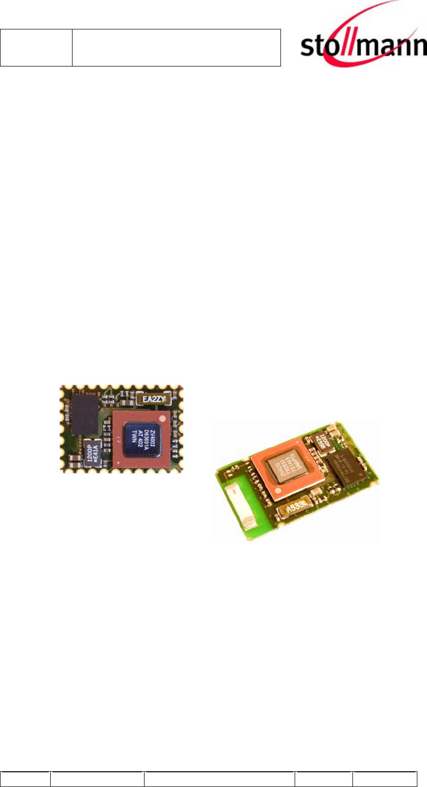
BlueMod+P24/P25 are short-range class 2 modules for implementing Bluetooth
functionality into various electronic devices. The modules consists of three major
parts; a baseband controller, a flash memory and a radio that operates in the
license-free 2.45 GHz ISM band.
The BlueMod+P25 is equipped with an internal antenna whereas the
BlueMod+P24 provides an 50 RF interface.
Both data and voice transmission are supported by the modules. Communication
between the modules and the host controller is carried out normally via UART,
USB and PCM interface.
Author: jw Date of Saving: 03.04.06 Ref: BlueMod+P2_HW_reference_V1_5.doc Revision: 1.5 Page 6 of 35
Stollmann
E + V GmbH
BlueMod+P24 / BlueMod+P25
Hardware reference
4 Scope of this Document
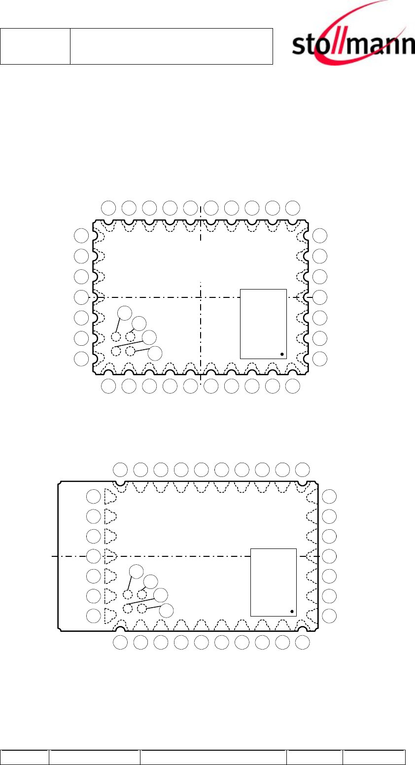
This product specification applies to the class 2 Bluetooth modules #52305
(BlueMod+P24) and #52287 (BlueMod+P25).
5 Terminal Layout
Top View
34
33
1 2 3 4 5 6 7 8 9 10
11
12
13
14
15
16
17
18192021222324252627
28
29
30
31
32
AB
C
D
Flash
4MBit
or
8MBit
BlueMod+P24
Top View
34
12345678910
11
12
13
14
15
16
17
18
19
20
21
22
23
24
25
26
27
28
29
30
31
32
AB
C
D
Flash
4MBit
or
8MBit
33
BlueMod+P25
Author: jw Date of Saving: 03.04.06 Ref: BlueMod+P2_HW_reference_V1_5.doc Revision: 1.5 Page 7 of 35
Stollmann
E + V GmbH
BlueMod+P24 / BlueMod+P25
Hardware reference
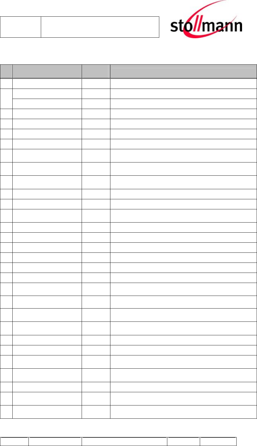
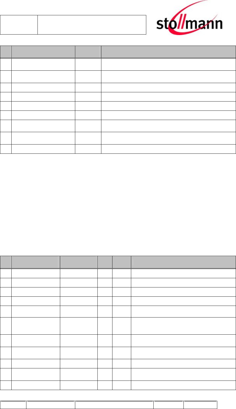
5.1 General Pin Assignment
Pin
No.
Pin
Name
Pin
Type Description
1 GND PWR ground connection (0Vdc)
BlueMod+P24: ANT 7.2 RF I/O 50 Ohm RX/TX connection to Antenna
2
BlueMod+P25: NC Not used
3 UART_RTS
7.4 I-PD UART Request To Send (active low)
4 UART_TXD
7.4 I-PD UART Data Input, w/ weak internal Pull-Down
5 UART_RXD
7.4 O UART Data Output
6 UART_CTS
7.4 O UART Clear To Send (active low), w/ weak internal Pull-Down
7 GPIO [9] (1)
PCM_CLK/INT2 I/O-PU General Purpose Input/Output with prog. weak internal
Pull-Up/PCM Data Clock Output/External Interrupt 2
8 GPIO [10] (1)
PCM_OUT/CS2 I/O-PU General Purpose Input/Output with prog. weak internal
Pull-Up/PCM Data Output/External Chip Select 2
9 GPIO [7] (1)
PCM_SYNC/INT1 I/O-PD General Purpose Input/Output with prog. weak internal
Pull-Down/PCM Data Sync Output/External Interrupt 1
10 GND PWR ground connection (0Vdc)
11 ATRST I-PD ARM JTAG reset (active low), Prog. Pull-Down
12 GPIO [8] (1)
PCM_IN/CS1 I/O-PU General Purpose Input/Output with prog. weak internal
Pull-Up/PCM Data Input/External Chip Select 1
13 ATDI I-PU ARM JTAG test data input, Prog. Pull-Up
14 ATMS I-PU ARM JTAG mode select, Prog. Pull-Up
15 reserved I
16 VCC I Positive supply +3,3Vdc (typical)
17 RESET7.3 I Reset input (active low for 5 ms); Schmitt triggered
18 GND PWR ground connection (0Vdc)
19 GPIO [14]
(1) I/O-PU
General Purpose Input/Output with prog. weak internal Pull-
Up
20 GPIO [13]
(1) I/O-PU
General Purpose Input/Output with prog. weak internal Pull-
Up
21 GPIO [15]
(1) I/O-PU
General Purpose Input/Output with prog. weak internal
Pull-Up(2)
22 GPIO [6]
(1) I/O-PD
General Purpose Input/Output with prog. weak internal
Pull-Down
23 ATDO O ARM JTAG test data output
24 ATCK I-PD ARM JTAG clock, Prog. Pull-Down
25 GPIO [3] (1)
SPI_CLK I/O-PD General Purpose Input/Output with prog. weak internal
Pull-Down/Serial Peripheral Interface Clock
26 GPIO [0] (1)
SPI_DO I/O-PD General Purpose Input/Output with prog. weak internal
Pull-Down/Serial Peripheral Interface Data Output
27 GND PWR Ground connection (0Vdc)
28 GPIO [2] (1)
SPI_CS I/O-PD General Purpose Input/Output with prog. weak internal
Pull-Down/Serial Peripheral Interface Chip Select
29 GPIO [1] (1)
SPI_DI I/O-PD General Purpose Input/Output with prog. weak internal
Pull-Down/Serial Peripheral Interface Data Input
Author: jw Date of Saving: 03.04.06 Ref: BlueMod+P2_HW_reference_V1_5.doc Revision: 1.5 Page 8 of 35
Stollmann
E + V GmbH
BlueMod+P24 / BlueMod+P25
Hardware reference
Pin
No.
Pin
Name
Pin
Type Description
30 GPIO [5]
DUART_TXD I/O-PD General Purpose Input/Output with prog. weak internal
Pull-Down/Debug UART Data Output
31 GPIO [4]
(1) DUART_RXD I/O-PD General Purpose Input/Output with prog. weak internal
Pull-Down/Debug UART Data Input
32 USB_DM7.5.1 I/O USB Data Minus terminal
33 USB_DP7.5.1 I/O USB Data Plus terminal
34 INT_0
(4) I External Interrupt
A reserved O
B GPIO [12] (1)
I/O-PU General Purpose Input/Output with prog. weak internal
Pull-Up/
C GPIO [11] (1)
I/O-PU General Purpose Input/Output with prog. weak internal
Pull-Up/
D NC Not used
Notes:
(1) The GPIO numbers refer to [1] chapter 25
(2) HCI Firmware: Pull up for USB or pull down for UART operation
(3) BlueMod+P25: All pins are land pattern pins, critical for hand soldering
BlueMod+P24: Pins A, B, C, D are land pattern pins, critical for hand
soldering
(4) subject to firmware support, contact Stollmann for current status
5.2 Application specific pin multiplexing
5.2.1 SPP configuration
Pin
No.
Pin
Name
SPP
function Dir. active Description
1 GND ground connection (0Vdc)
3 UART_RTS /RTS I L UART Request To Send (active low)
4 UART_TXD TxD I UART Data Input, w/ weak internal Pull-Down
5 UART_RXD RxD O UART Data Output
6 UART_CTS /CTS O L UART Clear To Send (active), w/ weak internal
Pull-Down
7 GPIO [9]
PCM_CLK/INT2 /LED2 O L
Bluetooth connected. Active if a Bluetooth
connection exists. Inactive in idle state. Flashes
during startup.
8 GPIO [10]
PCM_OUT/CS2 UA2 (2) O User Output 2
9 GPIO [7]
PCM_SYNC/INT1 /LED1 O L Device ready
10 GND ground connection (0Vdc)
12 GPIO [8]
PCM_IN/CS1 /UE (2) I L User Input
16 VCC I Positive supply +3,3Vdc (typical)
Author: jw Date of Saving: 03.04.06 Ref: BlueMod+P2_HW_reference_V1_5.doc Revision: 1.5 Page 9 of 35
Stollmann
E + V GmbH
BlueMod+P24 / BlueMod+P25
Hardware reference
Pin
No.
Pin
Name
SPP
function Dir. active Description
17 RESET I L Reset input (active low for 5 ms); Schmitt
triggered
18 GND ground connection (0Vdc)
19 GPIO [14] /RTC-OUT O L DSR in DCE mode, DTR in DTE mode
20 GPIO [13] /RTC-IN I L DTR in DCE mode, DSR in DTE mode
21 GPIO [15] /DCD or /DCD-
DTE O or
I L Data Carrier Detect , Input in DTE mode Output
in DCE mode
22 GPIO [6] /RI or /RI-DTE O or
I L Ring Indicator, Input in DTE mode Output in
DCE mode
25 GPIO [3]
SPI_CLK reserved
26 GPIO [0]
SPI_DO reserved I
27 GND Ground connection (0Vdc)
28 GPIO [2]
SPI_CS reserved O
29 GPIO [1]
SPI_DI reserved I User Input #2, Break detect (1)
30 GPIO [5]
DUART_TXD reserved O
31 GPIO [4]
DUART_RXD
DTE-/DCE
select I DTE (high) DCE (low) mode selector
B GPIO [12]
TX_EN reserved
C GPIO [11]
RX_EN reserved
All other Pins do not have a dedicated functionality in SPP mode. See 5.1 General
Pin Assignment for all other terminals.
Notes:
(1) Must be connected to RXD signal if break detection is needed (ask company
Stollmann for software support)
(2) subject to firmware support, contact Stollmann for current status.
5.2.2 AudioGateway/Headset – SPP configuration
Pin
No.
Pin
Name
Function Dir. Active Description
1 GND ground connection (0Vdc)
3 UART_RTS /RTS I L UART Request To Send (active low) low), w/
weak internal Pull-Down
4 UART_TXD TxD I UART Data Input, w/ weak internal Pull-Down
5 UART_RXD RxD O UART Data Output
6 UART_CTS /CTS O L UART Clear To Send (active
7 GPIO [9]
PCM_CLK/INT2 PCM_CLK O PCM Clock
Author: jw Date of Saving: 03.04.06 Ref: BlueMod+P2_HW_reference_V1_5.doc Revision: 1.5 Page 10 of 35
Stollmann
E + V GmbH
BlueMod+P24 / BlueMod+P25
Hardware reference
Pin
No.
Pin
Name
Function Dir. Active Description
8 GPIO [10]
PCM_OUT/CS2 PCM_OUT O PCM data Out
9 GPIO [7]
PCM_SYNC/INT1 PCM_SYNC O PCM Frame Sync
10 GND ground connection (0Vdc)
12 GPIO [8]
PCM_IN/CS1 PCM_IN I PCM Data input
16 VCC Positive supply +3,3Vdc (typical)
17 RESET I L Reset input (active low for 5 ms); Schmitt
triggered
18 GND ground connection (0Vdc)
19 GPIO [14] /DSR O L Data Set Ready
20 GPIO [13] /DTR I L Data Terminal Ready
21 GPIO [15] /DCD O L Data Carrier Detect
22 GPIO [6] CCD O L Codec Control Data
25 GPIO [3]
SPI_CLK HOOK_LED O L
26 GPIO [0]
SPI_DO CCC O Codec Control Clock
27 GND Ground connection (0Vdc)
28 GPIO [2]
SPI_CS STATE_LED O L
29 GPIO [1]
SPI_DI CSE O Codec Signal Enable
30 GPIO [5]
DUART_TXD MEA O Mute External Audio
31 GPIO [4]
DUART_RXD
CON-PAIR-
CONTROL I Init connection / pairing
B GPIO [12]
TX_EN /VDN I L Volume down – role Headset only
C GPIO [11]
RX_EN /VUP I L Volume up - role Headset only
All other Pins do not have a dedicated functionality in Audio Gateway / Headset
mode. See 5.1 General Pin Assignment for all other terminals.
Author: jw Date of Saving: 03.04.06 Ref: BlueMod+P2_HW_reference_V1_5.doc Revision: 1.5 Page 11 of 35
Stollmann
E + V GmbH
BlueMod+P24 / BlueMod+P25
Hardware reference
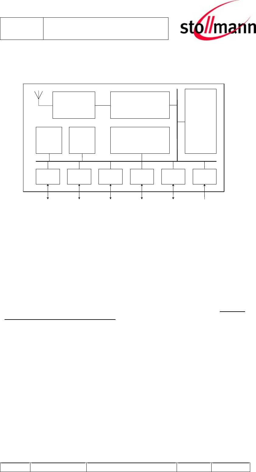
6 Block Diagram
A
RM7TDMI TM
MAC
Filter + Switch +
Matching Network
UART USB SPI GPIO PCM
Boot ROM RAM
4, 8, 16 MBit
Flash
INT
7 Terminal Specifics
7.1 Power supply
The BlueMod+P requires a power supply with the following characteristics:
3,3 V +- 9% low noise
100 mA peak
Due to the technological requirements and the pulsed radio transmission the
supply needs to be fed by an ultra fast linear regulator placed as close as possible
to the VCC pins. Functionality has been verified with the following types: TOREX:
XC6204B272MR or XC6401FF42MR
NOTE: You must ensure that the supply voltage never drops below 2.7 V. Otherwise
the flash contents (firmware and/or configuration data) can get lost.
7.2 RF-ANTENNA
The BlueMod+P24 presents a 50 impedance on the antenna pin.
The BlueMod+P25 presents an integrated ceramic antenna.
If the antenna performance fits not to your requirements or you need antenna
support please contact Stollmann.
It is highly recommended that you follow the design rule given in the Stollmann
Application Note on Antenna design [5].
Author: jw Date of Saving: 03.04.06 Ref: BlueMod+P2_HW_reference_V1_5.doc Revision: 1.5 Page 12 of 35
Stollmann
E + V GmbH
BlueMod+P24 / BlueMod+P25
Hardware reference
7.2.1 Typical Radiation Pattern
7.2.2 BlueMod+P25
A first idea can be seen in [3], the radiation pattern from the total module will be
delivered on request. Due to the compromise between module size and antenna
performance, the radiation pattern is a little bit worse against the optimal
circumstances, which are given in [3].
7.3 Reset
The RESET pin is an active low input that can be used to perform a full reset of the
device from an external signal. This pin does not contain an internal pull-up, so it
should be pulled-up externally if not used. The input is Schmitt triggered. A valid
reset signal must be low for at least 5 ms.
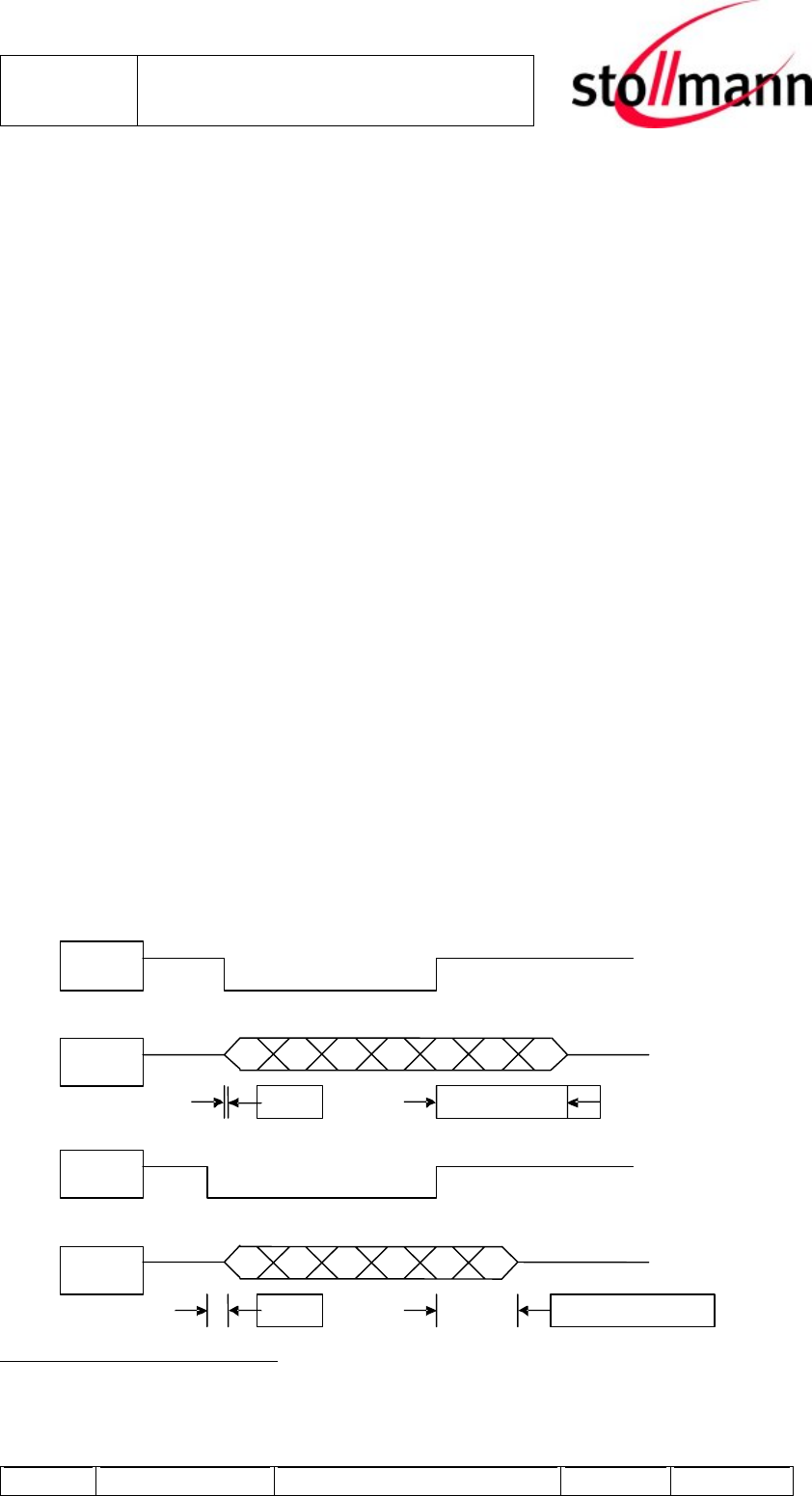
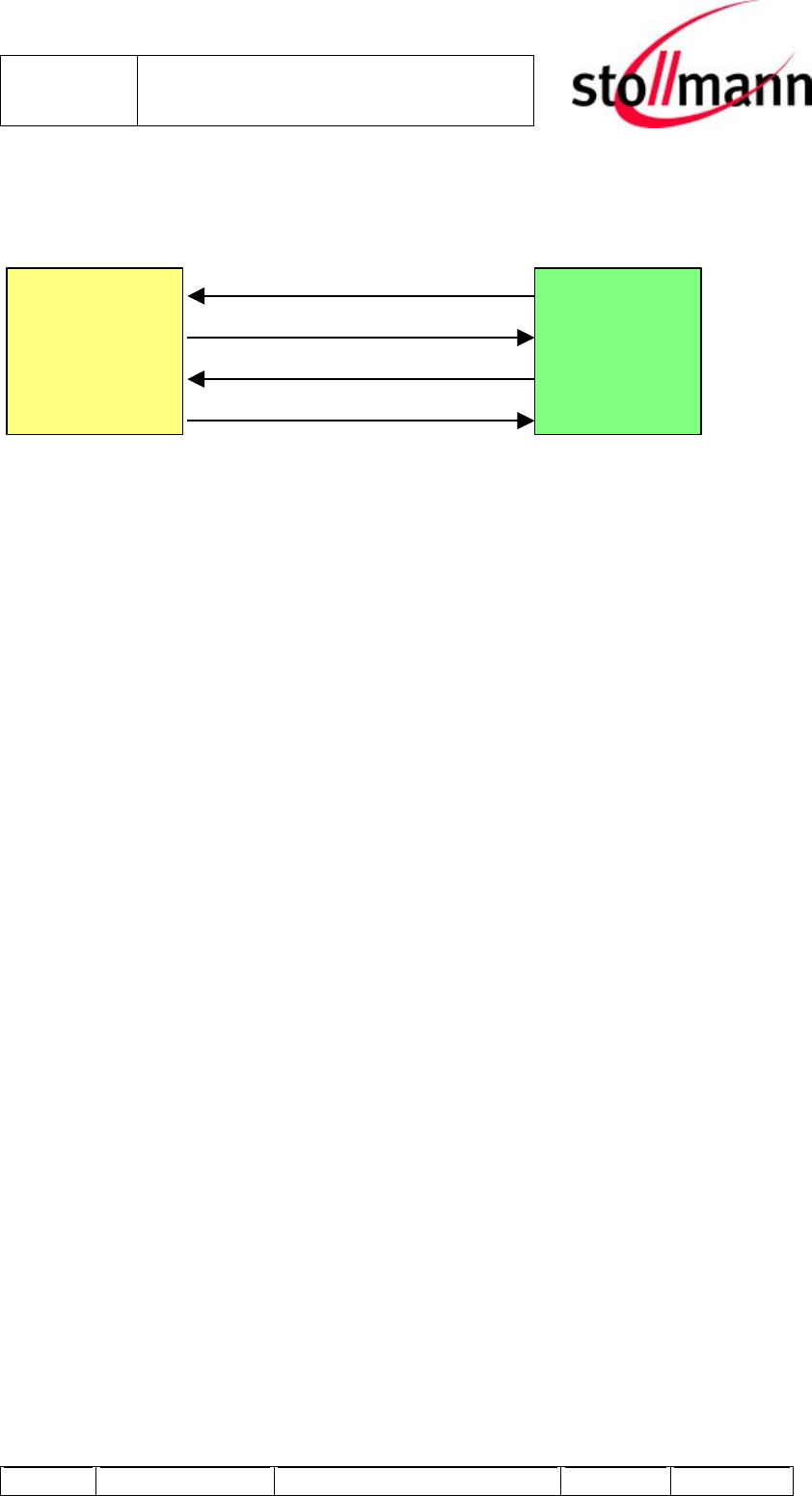
7.4 UART Interface – TXD, RXD, CTS, RTS
NOTE: All signals of the serial interface are named according to the EIA232 DTE
definition.
The UART is compatible with the 16450 industry standard and supports 9600, 19.2
K, 38.4 K, 57.6 K, 115.2 K, 230.4 K, 460.8 K, and 921.6 K bits/s 1 rates. Four
signals are provided with the UART interface. The TXD and RXD pins are used for
data while the CTS and RTS pins are used for flow control.
The character representation can be 7 or 8 data bit; no, even or odd Parity; 1 or 2
stop bits.
CTS
22 bytes max0 ns
TXD
RTS
1 character max82nS
RXD
1 subject to firmware support, contact Stollmann for current status
Author: jw Date of Saving: 03.04.06 Ref: BlueMod+P2_HW_reference_V1_5.doc Revision: 1.5 Page 13 of 35
Stollmann
E + V GmbH
BlueMod+P24 / BlueMod+P25
Hardware reference
Figure 1. UART Timing Diagram
BlueMod+P24
BlueMod+P25
DCE
Host
DTE
TXD
RX
D
RT
S
CTS
Figure 2. UART Signal Connections
7.5 USB Interface
7.5.1 D+, D-
The BlueMod+P24/P25 contains a full speed USB version 2.0 compliant interface
capable of directly driving a USB cable. The BlueMod+P24/P25 operates as a USB
peripheral and responds to requests from a USB master host controller. For the
BlueMod+P24/P25 to operate in USB mode, GPIO [15] must be pulled high.
Note: If your application requires operation in UART only mode, then
connecting the USB D+ pin to VCC and the USB D- to GND using 10k ohm
resistors will ensure that the USB circuit remains in an idle mode.
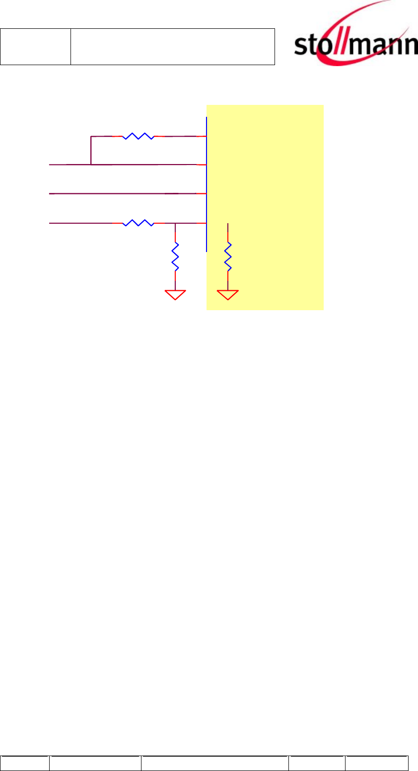
7.5.2 USB Pull-Up Resistor
A 1.5K pull up resistor needs to be connected between GPIO [2] and the USB D+
line. This pulls the USB D+ line high when the BlueMod+P24/P25 is ready for
enumeration, signaling to the host controller that the BlueMod+P24/P25 is a full
speed (12Mbps) USB device.
Author: jw Date of Saving: 03.04.06 Ref: BlueMod+P2_HW_reference_V1_5.doc Revision: 1.5 Page 14 of 35
Stollmann
E + V GmbH
BlueMod+P24 / BlueMod+P25
Hardware reference
7.5.3 USB Self-Powered Mode
BlueMod+P24
BlueMod+P25
GPIO[2] SPI_CS
28
USB_DP 33
USB_DM 32
GPIO[3] SPI_CLK 25
R1
R pull-up
1.5k
V
bus
D-
D+
R2 Rint ~50k
In USB self-
powered mode, the BlueMod+P24/P25 is powered from its own power supply and
not from the USB Vbus line. In order to detect when the USB Vbus line is powered
up, the USB Vbus line is monitored by GPIO [3] through a voltage divider formed
by R1 and Rint as shown in Figure 4. A 20K series resistor (R1) with a 50K
shunt resistor (Rint) will generate close to +3.3Vdc at the GPIO [3] pin. This will
produce around 55uA of leakage current through the voltage divider. If less
leakage current is desired, the internal pull down resistor can be disabled and an
external voltage divider (formed by R1 and R2) can be used to minimize the
leakage current.
Figure 3. Typical USB connection for Self Powered Mode
7.5.4 USB Bus-Powered Mode
In USB bus-powered mode, the BlueMod+P24/P25 is powered from the USB Vbus
line by means of a Low Drop Out (LDO) Voltage Regulator. When choosing the
LDO Voltage Regulator for supplying the +3.3V power to the BlueMod+P24/P25 ,
some factors that need to be considered are:
1. The voltage specification for the USB Vbus line is +4.75V to +5.25V.
2. The total current required (average and peak) for the design.
3. The voltage regulator’s drop out voltage vs. output current.
4. The voltage regulator’s power dissipation over the operating temperature range.
5. Filtering requirements on the USB Vbus line to attenuate noise above the
voltage regulator’s bandwidth.
6. The suspend state current draw.
Author: jw Date of Saving: 03.04.06 Ref: BlueMod+P2_HW_reference_V1_5.doc Revision: 1.5 Page 15 of 35
Stollmann
E + V GmbH
BlueMod+P24 / BlueMod+P25
Hardware reference
7.6 GPIO Interface
All GPIOs are capable of sinking and sourcing 2mA of I/O current. These terminals
are 5V tolerant.
NOTE: The designer should avoid applying a voltage to the GPIOs prior to
powering-up the device, this can cause reset stability issues with the
ZV4002/ZV4301 device.
GPIO [0] to GPIO [7] are internally pulled down with 50K (nominal) resistors.
GPIO [8] to GPIO [15] are internally pulled up with 50K (nominal) resistors.
The GPIO pins of the BlueMod+P24/P25 may be multiplexed with other functions as
described in chapter 0. This multiplexing is based on the application code loaded
into the BlueMod+P24/P25. In addition, certain GPIO pins have special functionality
based on the application.
GPIO [0] is used as the CODEC control clock for applications using an external
audio CODEC.
GPIO [1] is used as the CODEC signal enable for applications using an external
audio CODEC.
GPIO [2] is used for the USB D+ pull up through a 1.5 k Ohm resistor in USB mode.
GPIO [3] is the USB VBUS detect pin in USB mode.
GPIO [6] is the CODEC control data signal in applications using an external audio
CODEC.
GPIO [7] is the PCM SYNC signal in applications when an external CODEC is used.
GPIO [8] is the PCM IN signal in applications when an external CODEC is used.
GPIO [9] is the PCM CLK signal in applications when an external CODEC is used.
GPIO [10] is the PCM OUT signal in applications when an external CODEC is used.
Author: jw Date of Saving: 03.04.06 Ref: BlueMod+P2_HW_reference_V1_5.doc Revision: 1.5 Page 16 of 35
Stollmann
E + V GmbH
BlueMod+P24 / BlueMod+P25
Hardware reference
7.7 PCM Interface
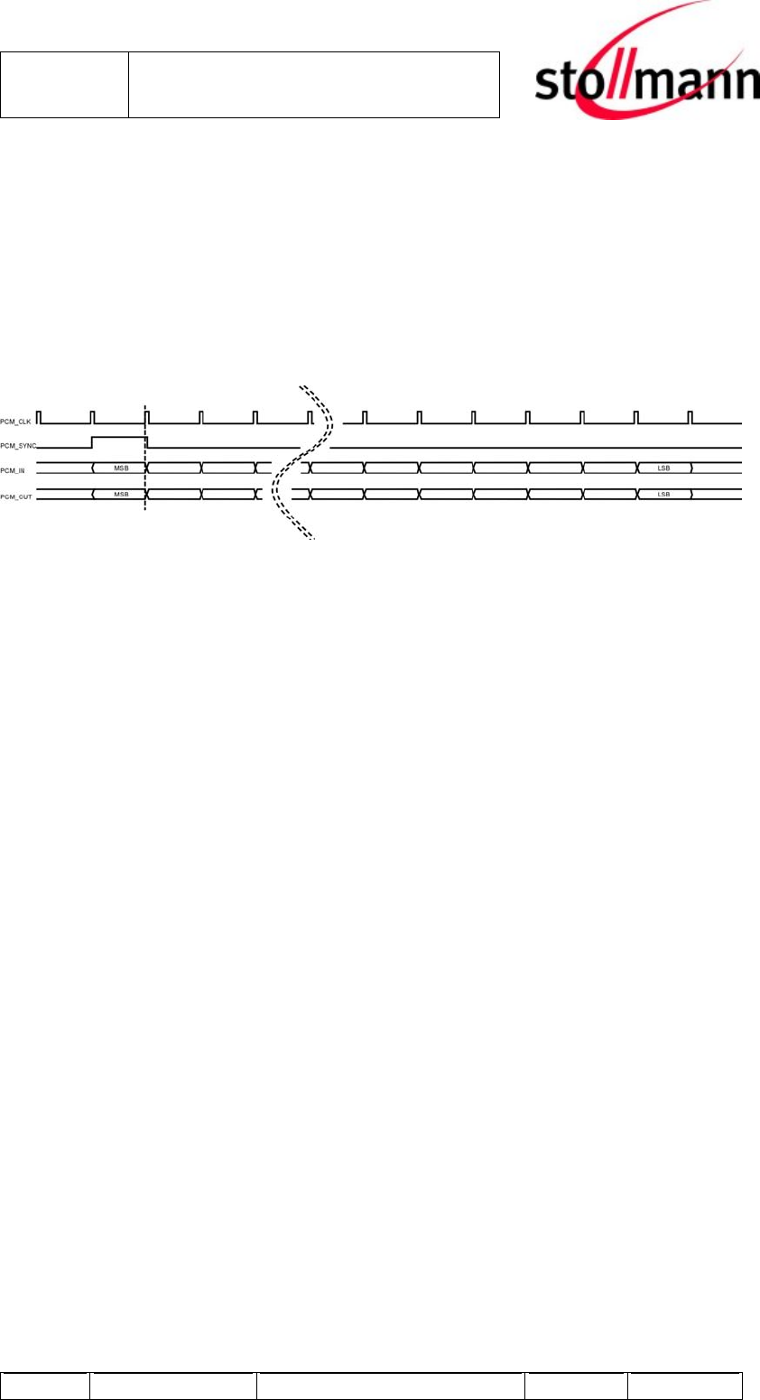
PCM or Pulse Code Modulation is a sampling technique for digitizing analog
signals. The PCM interface for voice applications is provided via the PCM_OUT,
PCM_IN, PCM_CLK and PCM_SYNC pins.
The PCM interface always acts as the master and uses a 1MHz bit clock. The Clock
duty cycle is 5% / 95%. The Frame Clock is 8Khz. The data format is 14bit linear
2th complement
Figure 4. PCM timing
The BlueMod+P24/P25 interfaces directly with the following CODECs:
OKI Semiconductor MSM 7732-01
OKI Semiconductor MSM 7716
In this scenario the use of GPIO [0], GPIO [1] and GPIO [6] is required to
control/program the CODEC.
Interface examples can be seen in [1] Figure 8 and 9.
8 Test Conditions
Measurements shall be made under room temperature and humidity unless
otherwise specified.
Temperature 25 ± 10°C Humidity 40 to 85%RH
Author: jw Date of Saving: 03.04.06 Ref: BlueMod+P2_HW_reference_V1_5.doc Revision: 1.5 Page 17 of 35
Stollmann
E + V GmbH
BlueMod+P24 / BlueMod+P25
Hardware reference
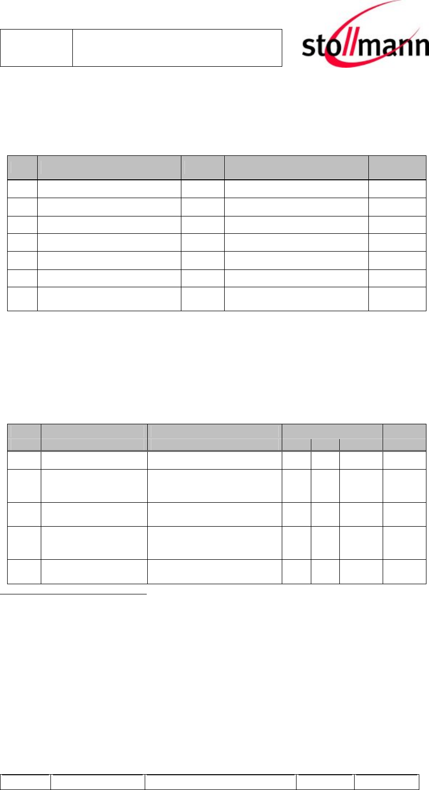
9 Absolute Maximum Ratings (1)
The maximum ratings may not be exceeded under any circumstances, not even
momentarily and individually, as permanent damage to the module will result.
No. Item Symbol Absolute Maximum Ratings Unit
1 Supply voltage Vcc -0.1 to +3.6 V
2 Voltage on any pin VPin -0.3 to Vcc+0.3 V
3 Storage temperature range Tstg -40 to +105 °C
4 Operating temperature range Top -25 to +85 °C
5 Input RF level Pmax 15 dBm
6 Lead temperature TDeath See chapter 16.2 °C
7 ESD on any pin VESD Max 2000 V
(CLoad = 150 pF, RLoad = 330) V
Note:
(1) Absolute Maximum Ratings indicate limits beyond which damage to the
device may occur.
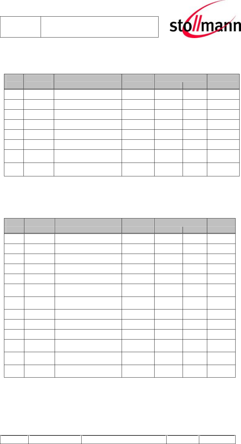
10 Electrical Requirements
Vcc = 3.3V, Tamb = 25°C if nothing else stated
No Item Condition Limit Unit
Min Typ Max
1 Frequency Range 2400 2483.5 MHz
2 Load impedance
Measured with network
analyzer in the frequency
range at antenna pin
50 Ω
3 Output return loss Receive Mode to 50 load
Transmit Mode to 50 load
-10
-10 dBm
4 Supply voltage.
The typical voltage is
recommended Vcc at voltage
pin
2.72
(3.0) 3.3 3.6 Vdc
5 Ripple on Vcc Ripple frequency ≥200kHz
Ripple frequency <200kHz tbd
tbd mVpp
2 valid for devices delivered since March 2006, the 2.7 V devices are labeled ENW89805J for
BlueMod+P25 and EN89803J for BlueMod+P24
Author: jw Date of Saving: 03.04.06 Ref: BlueMod+P2_HW_reference_V1_5.doc Revision: 1.5 Page 18 of 35
Stollmann
E + V GmbH
BlueMod+P24 / BlueMod+P25
Hardware reference
11 I/O Operating Characteristics
Vcc = 3.3V, Tamb = 25°C if nothing else stated
No Symbol Item Condition Limit Unit
Min Max Einheit
1 VIL Low-Level Input Voltage - 0.8 V
2 VIH High-Level Input Voltage 2.0 - V
3 VOL Low-Level Output Voltage IOL = 2mA - 0.3 V
4 VOH High-Level Output Voltage IOH = 2mA 2.8 3.6 V
5 IOL Low -Level Output Current VOL = 0.4V - 2.2 mA
6 IOH High-Level Output Current VOH = 2.4V - 3.1 mA
7 VT+ Schmitt Trigger Low to High
Threshold Pt. 1.47 1.50 V
8 VT- Schmitt Trigger High to Low
Threshold Pt. 0.89 0.95 V
12 USB I/O Operating Characteristics
Vcc = 3.3V, Tamb = 25°C if nothing else stated
No Symbol Item Condition Limit Unit
Min Max
1 VIL Low-Level Input Voltage - 0.8 V
2 VIH High-Level Input Voltage 2.0 - V
3 VOL Low-Level Output Voltage IOL = 2mA - 0.3 V
4 VOH High-Level Output Voltage IOH = 2mA 2.8 3.6 V
5 VDI Differential input sensitivity 0.2 - V
6 VCM Differential common-mode
range 0.8 2.5 V
7 VSE Single-ended receiver
threshold 0.8 2.0 V
8 VCRS Output Signal cross voltage 0.8 2.0 V
9 RPU Pull-up resistor 1.425 1.575
kΩ
10 RPD Pull-down resistor 1.425 1.575
kΩ
11 VTRM Termination voltage for
upstream port pull up (RPU) 3.0 3.6 V
12 ZDRV Driver output resistance Steady
State drive, 10 (typ)
Ω
13 Cin Input Capacitance DP or DM to
GND 20 pF
Author: jw Date of Saving: 03.04.06 Ref: BlueMod+P2_HW_reference_V1_5.doc Revision: 1.5 Page 19 of 35
Stollmann
E + V GmbH
BlueMod+P24 / BlueMod+P25
Hardware reference
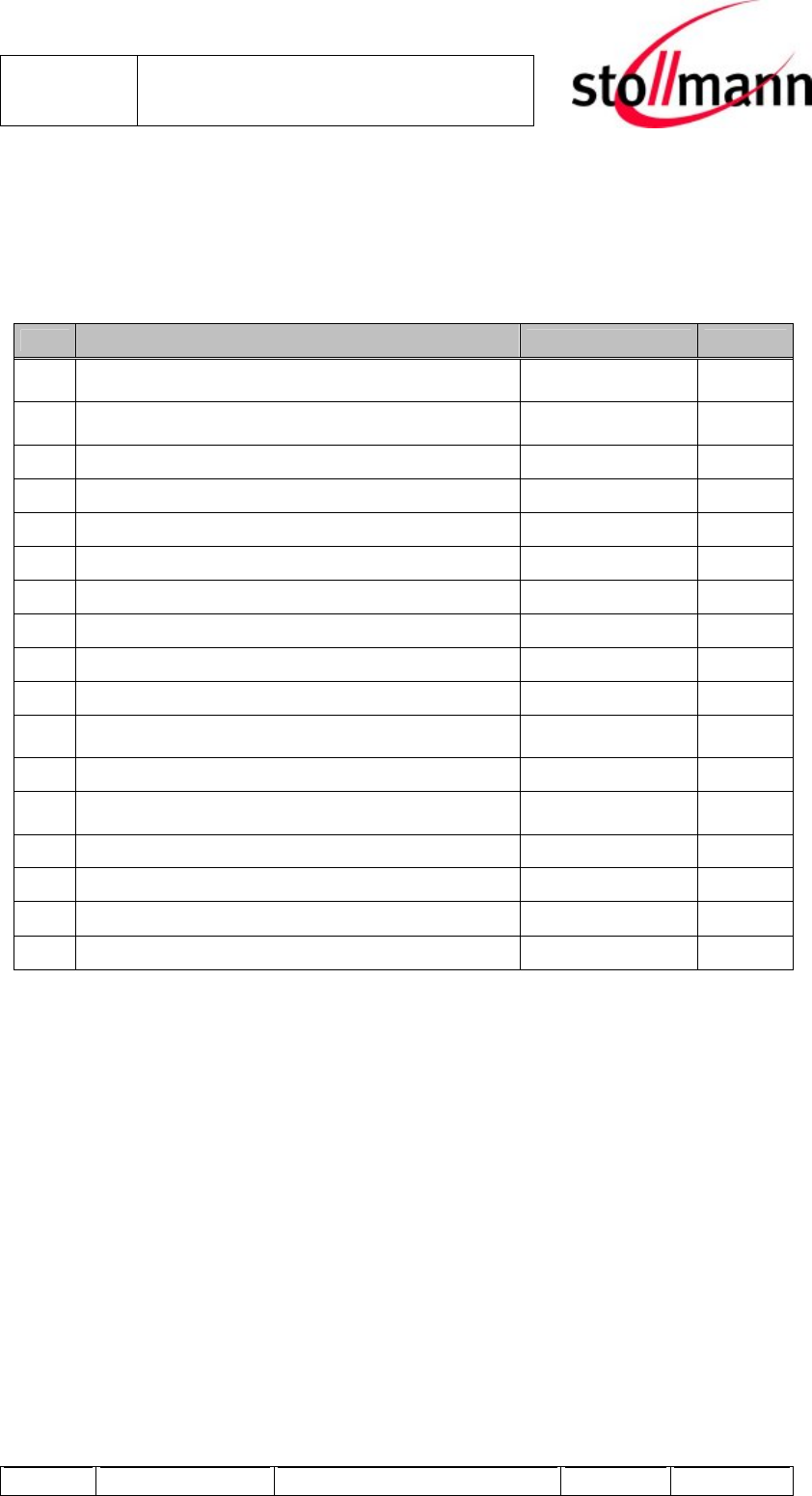
13 Typical Current Consumption
13.1 HCI Configuration
Vcc = 3.3V, Tamb = 25°C, F = 2402 – 2480GHz, 50Ω antenna
No Modes Average Unit
1 ACL data over 115K Baud UART at maximum
throughput (Master) 33.3 mA
2 ACL data over 115K Baud UART at maximum
throughput (Slave) 30.26 mA
3 ACL data over USB at maximum throughput (Master) 43 mA
4 ACL data over USB at maximum throughput (Slave) 43.6 mA
5 SCO connection HV1, master 40 mA
6 SCO connection HV1, slave 40 mA
7 SCO connection HV3, master 34.0 mA
8 SCO connection HV3, slave 31.0 mA
9 Connection, no data traffic, master 20 mA
10 Connection, no data traffic, slave 28.5 mA
11 Connection in sniff (Tsniff=100ms), no data traffic,
master 7.5 mA
12 Connection in sniff (Tsniff=100ms), no data traffic, slave 7.6 mA
13 Connection in sniff (Tsniff=375ms), no data traffic,
master 2.1 mA
14 Connection in sniff (Tsniff=375ms), no data traffic, slave 2.2 mA
15 No scan, deep sleep (including on-die regulator) 0.140 mA
16 Page/Inquiry scan 0.5 mA
17 Peak current 50 mA
Author: jw Date of Saving: 03.04.06 Ref: BlueMod+P2_HW_reference_V1_5.doc Revision: 1.5 Page 20 of 35
Stollmann
E + V GmbH
BlueMod+P24 / BlueMod+P25
Hardware reference
13.2 SPP configuration
13.2.1 Deep Sleep state
The Bluetooth RF is completely deactivated, no paging requests from other
Bluetooth devices will be recognized. Only rising control line DTR will activate the
BlueMod+P24/P25 and may initiate a Bluetooth link dependent on other parameters.
Note: In Deep Sleep state the AT command set is not active, CTS line is low.
13.2.2 Power down state
The Bluetooth RF is activated every 1.25 seconds, paging requests from other
Bluetooth devices will be recognized after that intervals and accepted if allowed.
Additionally rising control line DTR will activate the BlueMod+P24/P25 and may
initiate a Bluetooth link dependent on other parameters.
Note: In Power down state the AT command set is not active, CTS line is low.
13.2.3 Idle state
No power down mode activated.
All functionality is available immediately including connection control using AT
command set.
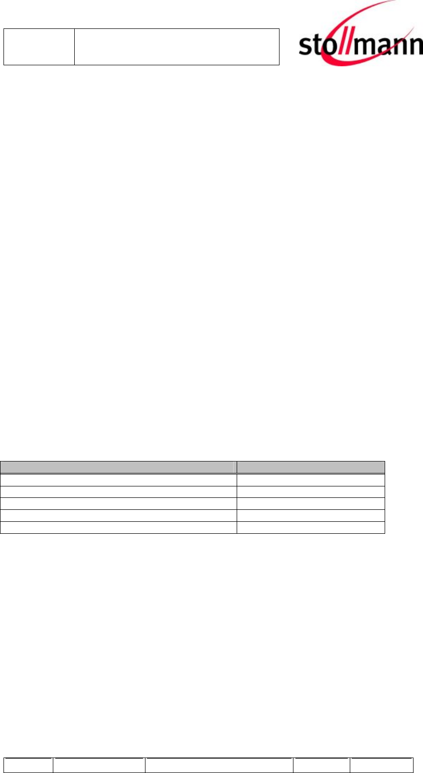
13.2.4 Power consumption
The following values are approximate power consumption values in the different
states:
Condition Current Consumption average
Deep sleep 1 ~ 0.7 mA
Power down (average) ~1.8 mA
Idle, all functions available, no Bluetooth link 19 mA
Bluetooth connected, no data traffic, (master/slave) 19/32 mA
Bluetooth connected, data traffic 115 kbit/s 44 mA
1 RXD,TXD,RTS,CTS lines connected - parameters cdcd=0, bpsm=0, pwd=1
Author: jw Date of Saving: 03.04.06 Ref: BlueMod+P2_HW_reference_V1_5.doc Revision: 1.5 Page 21 of 35
Stollmann
E + V GmbH
BlueMod+P24 / BlueMod+P25
Hardware reference
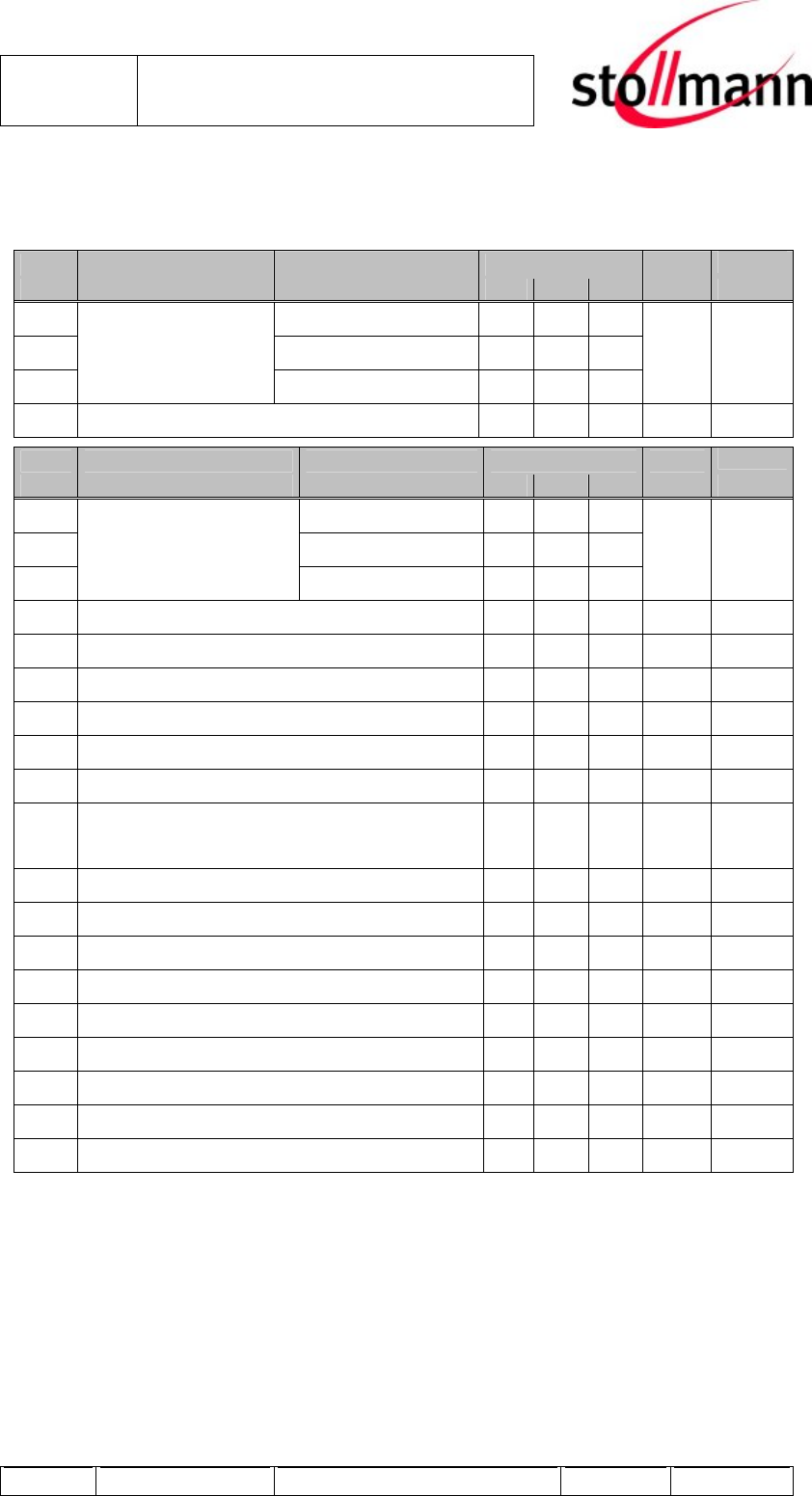
14 Electrical RF-Characteristics
Vcc = 3.3V, Tamb = 25°C, 50Ω antenna
No Receiver Frequency [GHz] Limit BT Unit
Min Typ Max Spec
1 2.402 - -85 -
2 2.441 - -85 -
3
Sensitivity at 0.1% BER
2.480 - -85 -
≤-70 dBm
4 Maximum received signal at 0.1% BER with DH1 - -5 - ≥-20 dBm
No Transmitter Frequency [GHz] Limit BT Unit
Min Typ Max Spec
5 2.402 - 0 4
6 2.441 - 0 4
7
RF transmit power
50 load, at antenna
Class 2 device 2.480 - 0 4
-6 to
+4 dBm
8 RF power control range - 30 - ≥16 dB
9 RF power range control resolution - 4 - 2 to 8 dB
10 20 dB bandwidth for modulated carrier - 930 - ≤1000 kHz
11 Initial carrier frequency tolerance -10 0 +12 ≤ ±75 kHz
12 Carrier frequency drift (packet DH1) - ±4 ±8 ≤ ±25 kHz
13 Drift Rate - 60 210 400 Hz/µs
14 ∆f1avg “Maximum Modulation” 145 166 170
≥140
to
≤175
kHz
15 ∆f2avg “Minimum Modulation” 110 160 - ≥ 115 kHz
16 C/I co-channel <11 - (1) ≤ 11 dB
17 Adjacent channel selectivity C/I f = f0 ± 1MHz 0 - (1) ≤ 0 dB
18 Adjacent channel selectivity C/I f = f0 ± 2MHz <-30 - (1) ≤ -30 dB
19 Adjacent channel selectivity C/I f ≥ f0 +3MHz <-40 - (1) ≤ -40 dB
20 Adjacent channel selectivity C/I f ≤ f0 -3MHz <-40 - (1) ≤ -40 dB
21 Adjacent channel selectivity C/I f = fimage <-9 -
(1) ≤ -9 dB
22 Adjacent channel Transmit power f = f0 ± 2MHz -39 -43 -47 ≤ -20 dBc
23 Adjacent channel Transmit power f = f0 ± 3MHz -45 -48 -52 ≤ -40 dBc
Note:
(1) The tests was made to the bluetooth regulation, with the BER limit of 0,1%.
With the output limits given as a minimum value, there was no bit error
failure and the test was pass. Therefore the maximum values are not
measured.
Author: jw Date of Saving: 03.04.06 Ref: BlueMod+P2_HW_reference_V1_5.doc Revision: 1.5 Page 22 of 35
Stollmann
E + V GmbH
BlueMod+P24 / BlueMod+P25
Hardware reference
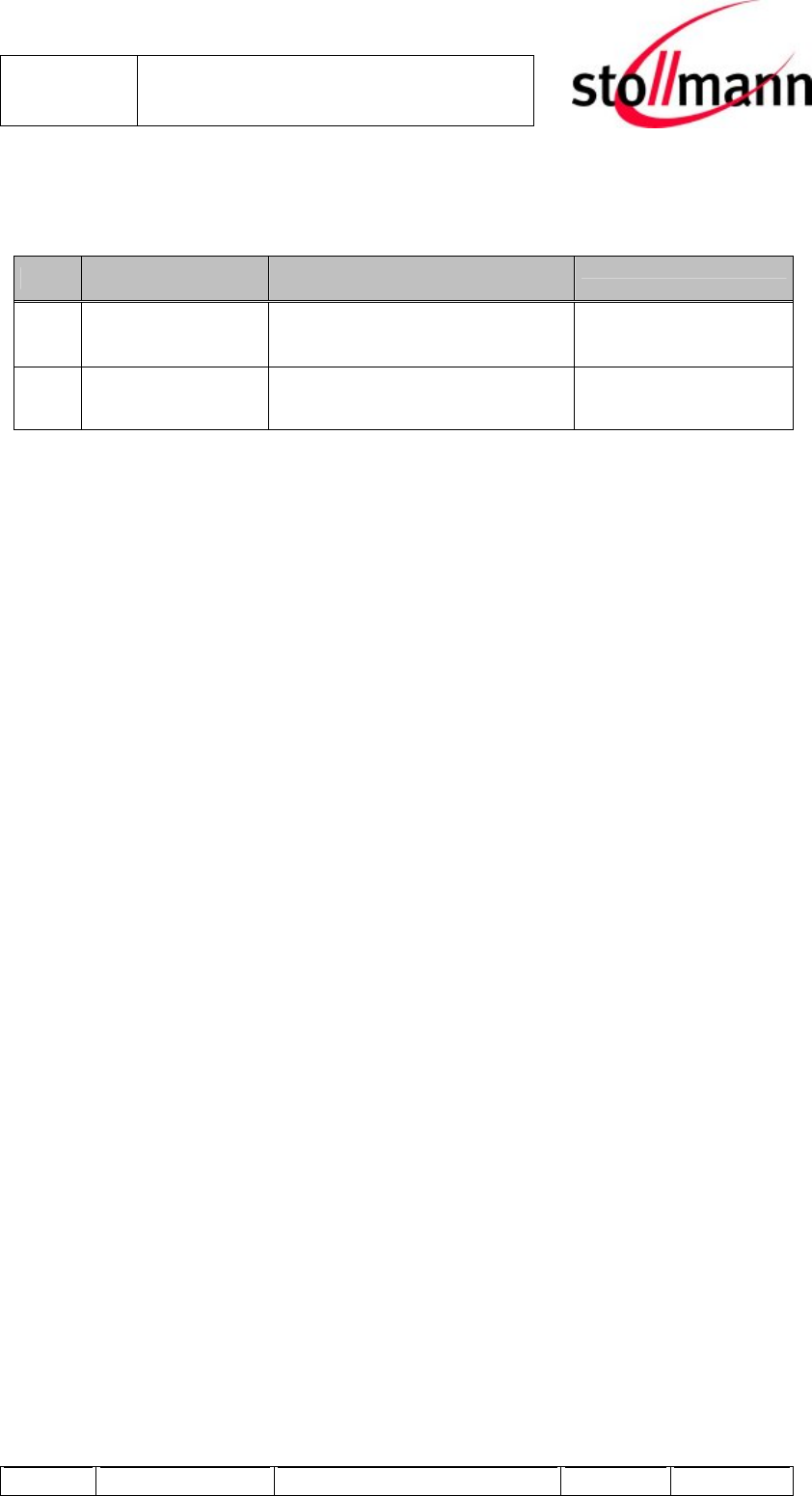
15 Mechanical Requirements
No. Item Limit Condition
1 Solderability
More than 75% of the soldering area
shall be coated by solder
Reflow soldering with
recommendable
temperature profile
2 Resistance to
soldering heat
It shall be satisfied electrical
requirements and not be mechanical
damage
See chapter 16.2
Author: jw Date of Saving: 03.04.06 Ref: BlueMod+P2_HW_reference_V1_5.doc Revision: 1.5 Page 23 of 35
Stollmann
E + V GmbH
BlueMod+P24 / BlueMod+P25
Hardware reference
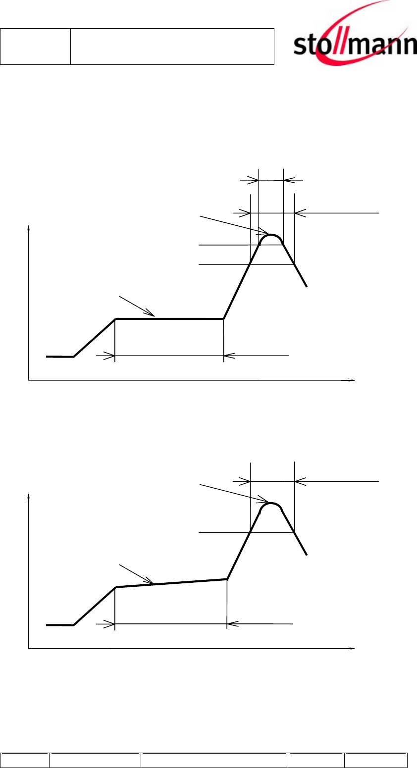
16 Soldering Temperature-Time Profile (for reflow soldering)
16.1 For lead solder
Recommended temp. profile
for reflow soldering
Tem
p
.
[
°C
]
Time [s]
235°C max.
220
±
5°C
200°C
150 ±10°C
90 ±30s
10 ±1s
30 +20/-10s
16.2 For lead-free solder
Our used temp. profile
for reflow soldering
Temp.[°C]
Time [s]
230°C -250°C max.
220°C
150°C – 190°C
90 ±30s
30 +20/-10s
Reflow permissible cycle: 2
Opposite side reflow is prohibited due to module weight.
The critical componet is the Zeevo chip, if you are not able to use our temperature
profile please check [4] page 5 in chapter 30.
Author: jw Date of Saving: 03.04.06 Ref: BlueMod+P2_HW_reference_V1_5.doc Revision: 1.5 Page 24 of 35
Stollmann
E + V GmbH
BlueMod+P24 / BlueMod+P25
Hardware reference
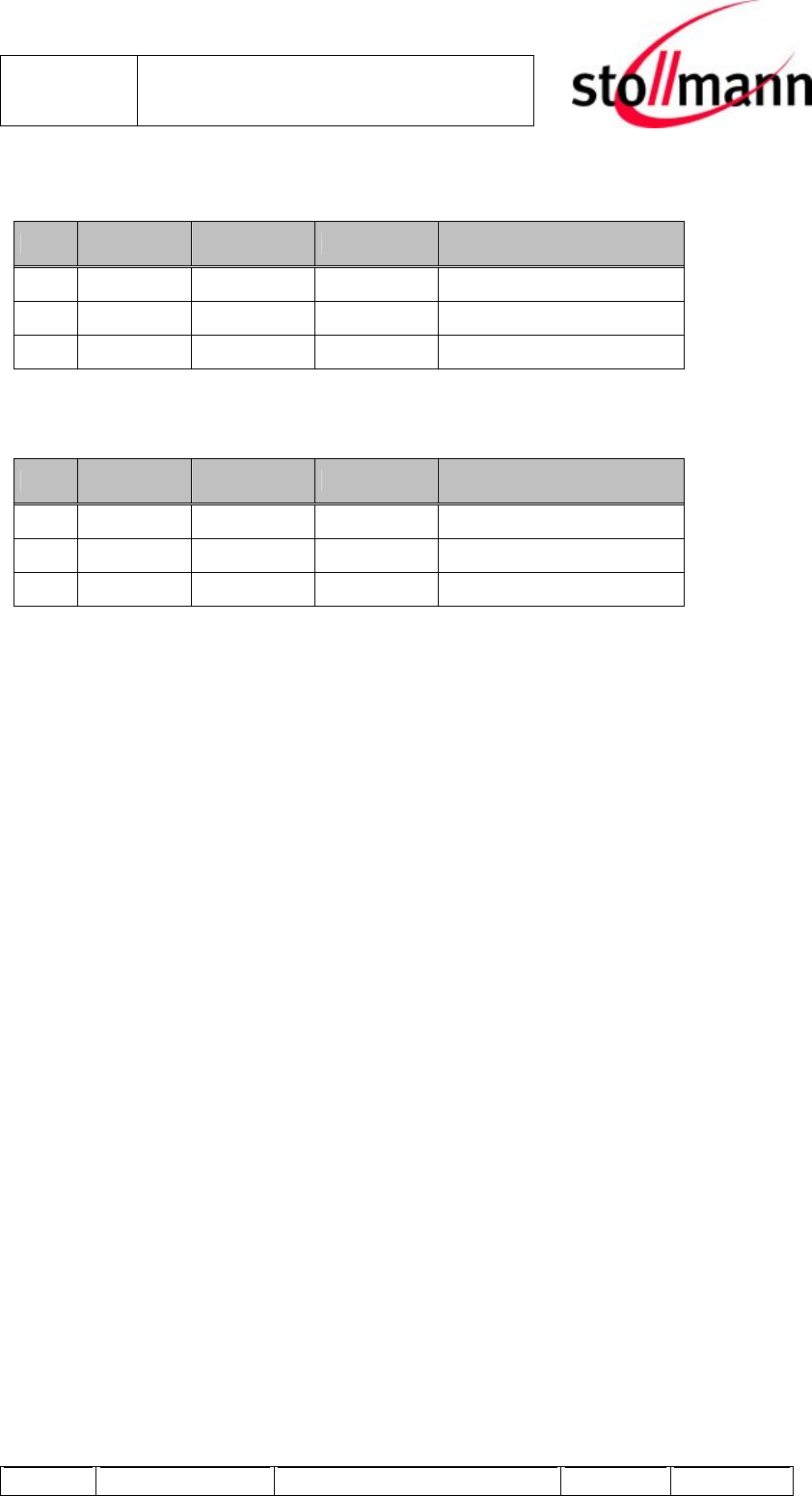
17 Module Dimension
No. Item Dimension Tolerance Remark
1 Width 13.34 ± 0.1
2 Lenght 18.65 ± 0.1
3 Hight 2.13 ± 0.05
BlueMod+P24
No. Item Dimension Tolerance Remark
1 Width 13.34 ± 0.1
2 Lenght 22.75 ± 0.1
3 Hight 2.13 ± 0.05 Without casing
BlueMod+P25
Author: jw Date of Saving: 03.04.06 Ref: BlueMod+P2_HW_reference_V1_5.doc Revision: 1.5 Page 25 of 35
Stollmann
E + V GmbH
BlueMod+P24 / BlueMod+P25
Hardware reference
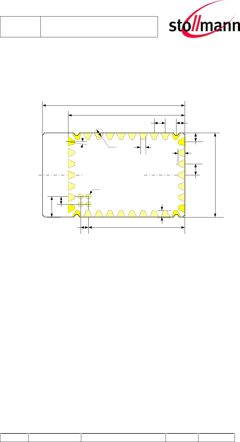
18 Foot Print of the Modules
18.1 Engineering sample status
Top View
1.25
4 x Ø0.80
P=1.77
1.08
1.08
1.36
P=1.77
0.80
1.36
3.25
15.40
1.25
13.34
±0.1
22.75
±0.1
18.65
Ø1.35
10,0°
BlueMod+P25, Dimension in mm
Author: jw Date of Saving: 03.04.06 Ref: BlueMod+P2_HW_reference_V1_5.doc Revision: 1.5 Page 26 of 35
Stollmann
E + V GmbH
BlueMod+P24 / BlueMod+P25
Hardware reference
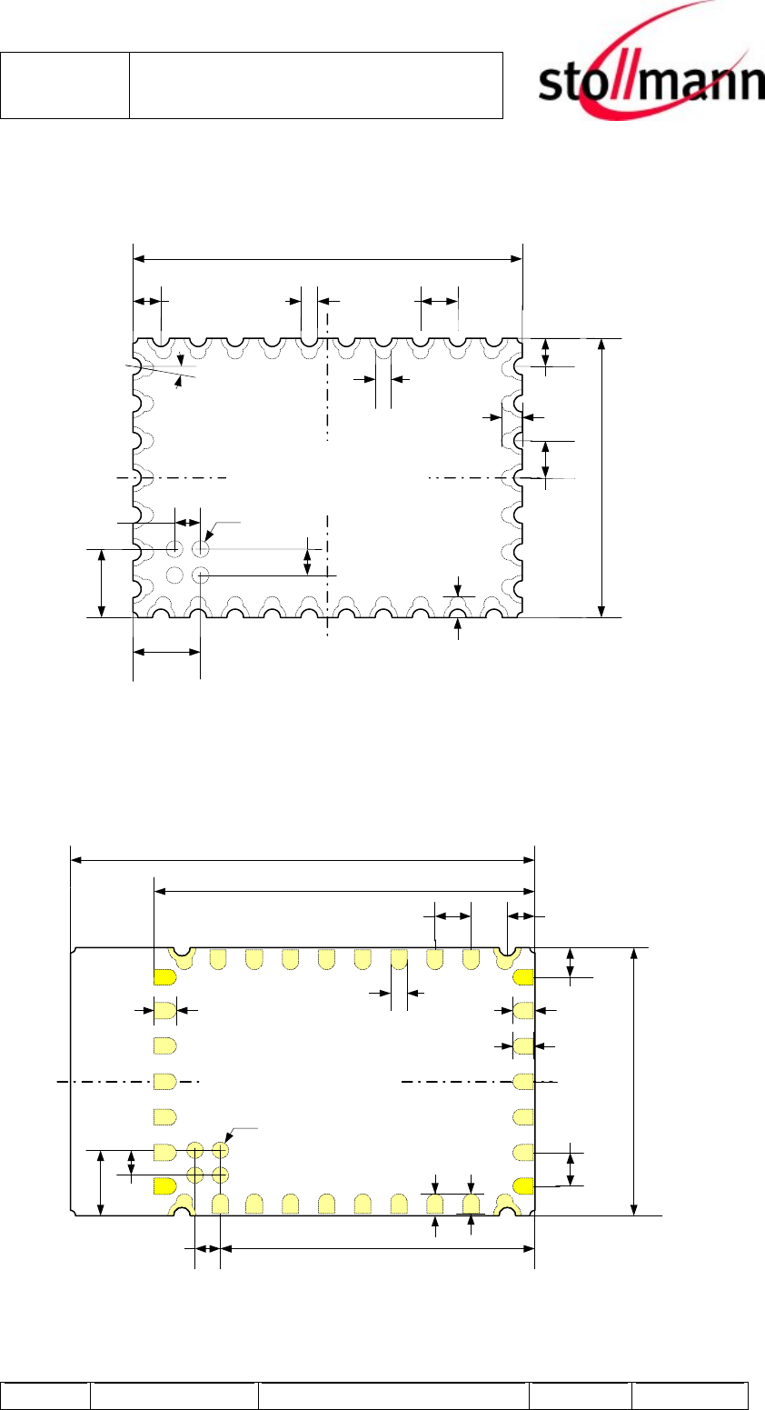
18.2 Mass production status
Top View
P=1.77
1.00
1.00
1.36
10,0°
P=1.77
0.75
18.65
13.34
1.36
0.80
1.25
3.25
3.25
1.25 R 0.4
BlueMod+P24, Dimension in mm
Top View
1.25
4 x Ø0.80
26 x P1=1.77
1.08
0.99
1.36
0.80
1.46
3.25
15.40
1.25
13.34
±0.1
22.75
±0.1
18.65
1.08
4 x P2=1.67
1.08
0.99
BlueMod+P25, Dimension in mm
Author: jw Date of Saving: 03.04.06 Ref: BlueMod+P2_HW_reference_V1_5.doc Revision: 1.5 Page 27 of 35
Stollmann
E + V GmbH
BlueMod+P24 / BlueMod+P25
Hardware reference
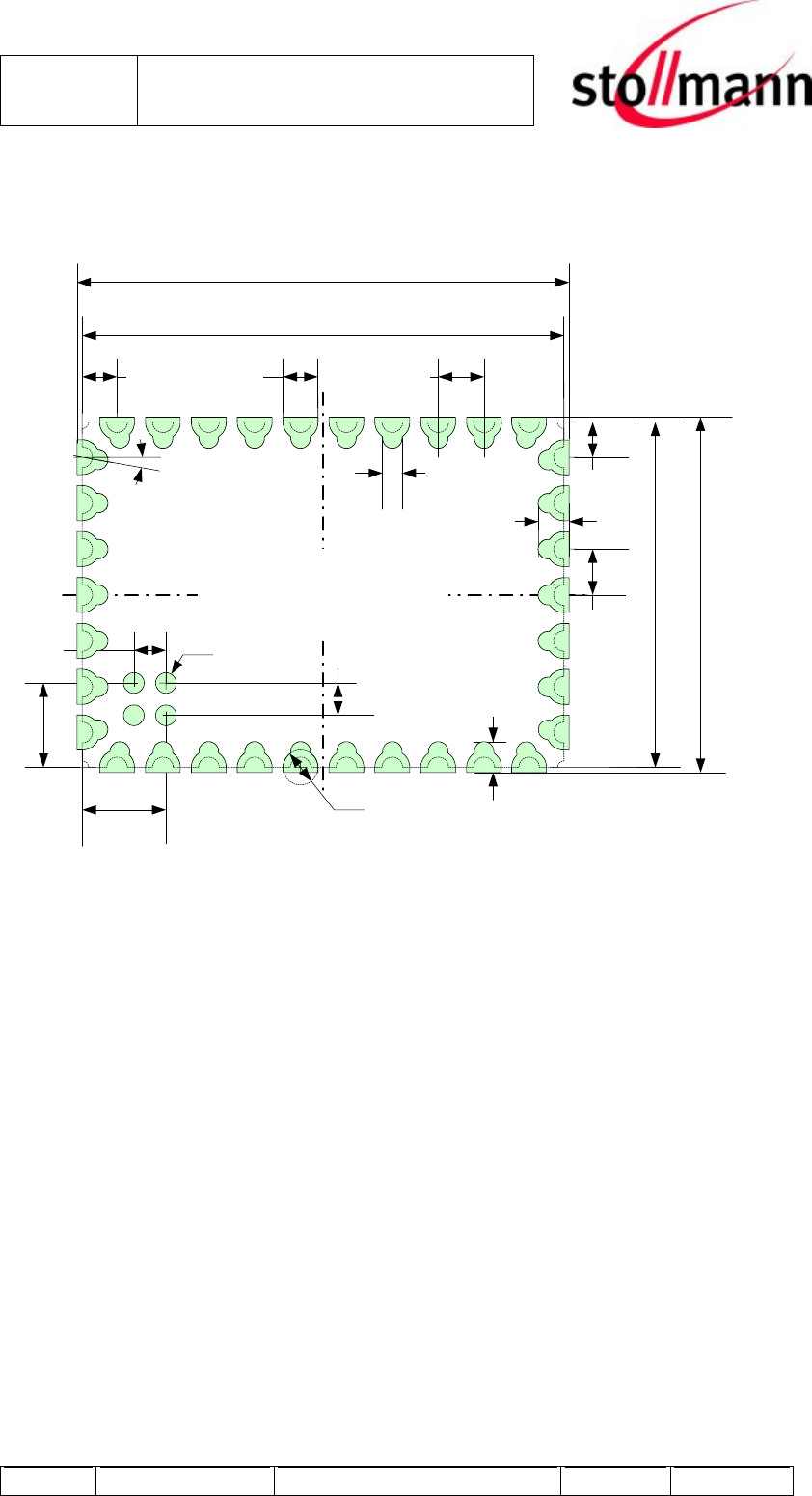
19 Recommended Foot Pattern
Top View
P=1,77
1.20
1.20
1.36
P=1.77
0.75
18.65
13.34
1.36
1.35
1.25
3.25
3.25
1.25
Ø1,35
19,05
13.74
Ø0,80
10,0°
BlueMod+P24 Foot Pattern
Author: jw Date of Saving: 03.04.06 Ref: BlueMod+P2_HW_reference_V1_5.doc Revision: 1.5 Page 28 of 35
Stollmann
E + V GmbH
BlueMod+P24 / BlueMod+P25
Hardware reference
Top View
22 x P1=1,77
0.70
1.25
3.45
3.45
1.25
19.05
13.74
4 x Ø0,80
1.31
1.31
8 x P2=1,67
1.31 1.31
5.0
5.0
Antenna
Restricted
Area
(no ground)
22.75 (Module Length)
1.10
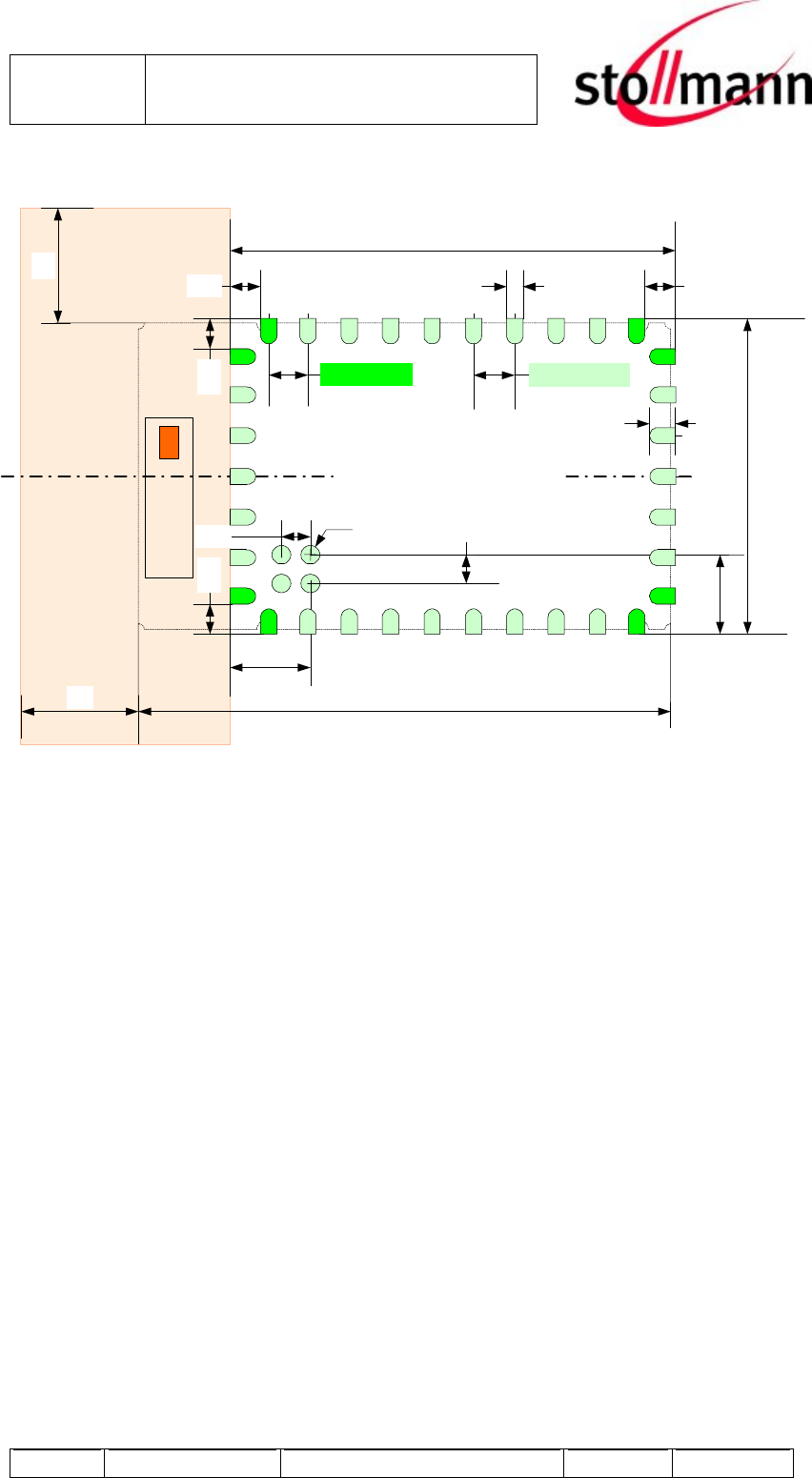
BlueMod+P25 Foot Pattern
If you have no experience about the land pattern, this figure can guide you, but this
information is given without any legal responsibility.
We recommend the same dimension for the solder paste screen.
The solder screen thickness depends on your production standard, we recommend
120µm to 150µm.
IMPORTANT:
Please be careful with the area under the module to avoid short cuts.
Engineering Sample Status:
The bottom side from the BlueMod+P24/P25 is fully coated, except the vias!
Mass Production Status:
The bottom side from the BlueMod+P25 is fully coated, also the vias!
To give an optimized antenna performance the restricted area should have no
ground and the minimum dimension should be carry out, depending on your
possible space.
If you have any questions on this point, we are open to discuss your individual
situation.
Author: jw Date of Saving: 03.04.06 Ref: BlueMod+P2_HW_reference_V1_5.doc Revision: 1.5 Page 29 of 35
Stollmann
E + V GmbH
BlueMod+P24 / BlueMod+P25
Hardware reference
20 Reliability Tests
The measurement should be done after exposed to room temperature and
humidity for 1hour.
No. Item Limit Condition
1 Vibration test
Electrical parameter should
be in specification
a) Freq.:10~50Hz,Amplitude:1.5mm
a) 20min. / cycle,1hrs. each of XYZ axis
b) Freq.:30~100Hz, 6G
b) 20min. / cycle,1hrs. each of XYZ axis
2 Shock test the same as the above Dropped onto hard wood from height of
50cm for 3 times
3 Heat cycle test the same as the above -40°C for 30min. and +85°C for 30min.;
each temperature 300 cycles
4 Moisture test the same as the above +60°C, 90% RH, 300h
5 Low temp. test the same as the above -40°C, 300h
6 High temp. test the same as the above +85°C, 300h
Author: jw Date of Saving: 03.04.06 Ref: BlueMod+P2_HW_reference_V1_5.doc Revision: 1.5 Page 30 of 35

Stollmann
E + V GmbH
BlueMod+P24 / BlueMod+P25
Hardware reference
21 Regulatory Information
21.1 Declaration of conformity
21.2 FCC Compliance
21.2.1 FCC Statement
This device complies with Part 15 of the FCC Rules and with RSS-210 of Industry
Canada.
Operation is subject to the following two conditions:
(1) this device my not cause harmful interference, and
(2) this device must accept any interference received, including interference
that may cause undesired operation.
21.2.2 Caution
Warning: Changes or modifications made to this equipment not expressly approved
by Stollmann Entwicklungs und Vertriebs may void the FCC authorization to operate
this equipment.
21.2.3 FCC Warning
This equipment has been tested and found to comply with the limits for a Class B
digital device, pursuant to Part 15 of the FCC Rules. These limits are designed to
provide reasonable protection against harmful interference in a residential
installation. This equipment generates, uses and can radiate radio frequency
energy and, if not installed and used in accordance with the instructions, may cause
harmful interference to radio communications. However, there is no guarantee that
interference will not occur in a particular installation. If this equipment does cause
harmful interference to radio or television reception, which can be determined by
turning the equipment off and on, the user is encouraged to try to correct the
interference by one or more of the following measures:
• Reorient or relocate the receiving antenna.
• Increase the separation between the equipment and receiver.
• Connect the equipment into an outlet on a circuit different from that to which the
receiver is connected.
Consult the dealer or an experienced radio/TV technician for help.
Author: jw Date of Saving: 03.04.06 Ref: BlueMod+P2_HW_reference_V1_5.doc Revision: 1.5 Page 31 of 35
Stollmann
E + V GmbH
BlueMod+P24 / BlueMod+P25
Hardware reference
The radiated output power of BlueMod+P24/P25 is far below the FCC radio
frequency exposure limits. Nevertheless, the BlueMod+P24/P25 shall be used in
such a manner, that the potential for human contact during normal operation is
minimized.
21.2.4 RF-exposure Statement
The BlueMod+P24/P25 contains a portable modular transmitter. Thus it must have a
separation of at least 2.5 cm between the antenna and the body of the user or
nearby persons, excluding hands, wrists, feet, and ankles.
Any notification to the end user of installation or removal instructions about the
integrated radio module is not allowed.
21.2.5 Labelling requirements for the End Product
Any End Product integrating the BlueMod+P24/P25 must be labeled with at least the
following information:
This device contains transmitter with
FCCID: RFR-BRSI2 /IC: 4957A-BRSI2
22 RoHS Declaration
Declaration of environmental compatibility for supplied products:
Hereby we declare to our best present knowledge based on declaration of our
suppliers that this product do not contain by now the following substances which
are banned by Directive 2002/95/EC (RoHS) or if contain a maximum
concentration of 0,1% by weight in homogeneous materials for
• Lead and lead compounds
• Mercury and mercury compounds
• Chromium (VI)
• PBB (polybrominated biphenyl) category
• PBDE (polybrominated biphenyl ether) category
And a maximum concentration of 0,01% by weight in homogeneous materials for
• Cadmium and cadmium compounds
Author: jw Date of Saving: 03.04.06 Ref: BlueMod+P2_HW_reference_V1_5.doc Revision: 1.5 Page 32 of 35

Stollmann
E + V GmbH
BlueMod+P24 / BlueMod+P25
Hardware reference
23 Data Sheet Status
Supplementary data will be published at a later date. Stollmann reserves the right
to change the specification without notice, in order to improve the design and
supply the best possible product.
Please consult the most recently issued data sheet before initiating or completing a
design.
Author: jw Date of Saving: 03.04.06 Ref: BlueMod+P2_HW_reference_V1_5.doc Revision: 1.5 Page 33 of 35
Stollmann
E + V GmbH
BlueMod+P24 / BlueMod+P25
Hardware reference
24 Ordering Information
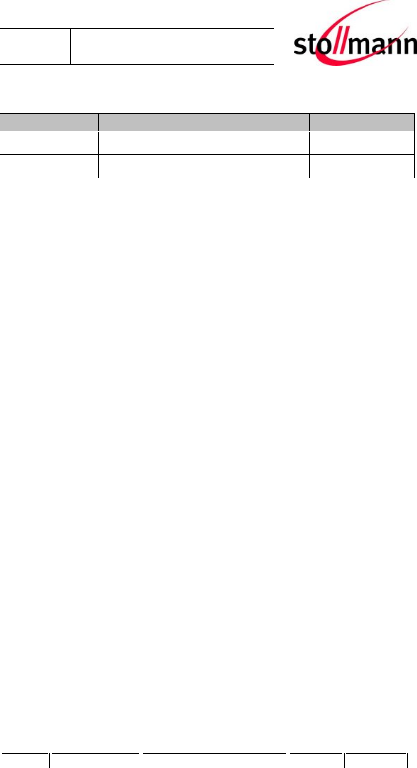
Ordering part number Description MOQ
# 52305 BlueMod+P24
Bluetooth module, class 2, without antenna 1
# 52287 BlueMod+P25
Bluetooth module, class 2, integrated antenna 1
25 Related Documents
[1] ZV4002 Hardware Design Guide APP-1034 Version 2.1 08 Jul 2004
[2] Data Sheet ZV4002 Preliminary Release Version 3.1 Feb. 05, 2004
[3] Data Sheet 2.45 GHz Antenna Part Number: 2450AT43A100, Johanson
Technology, 12/21/03
[4] AN-01 Soldering Reflow and Rework Guidelines Zeevo Rev. 3.2
29. November 2004
[5] Application note Antenna Design AN_B0601_Antenna_Design V1.0,
Stollmann GmbH
26 General Information
If we deliver samples to the customer, these samples have the status Engineering
Samples. This means, the design of this product is not yet concluded. Engineering
Samples may be partially or fully functional, and there may be differences to be
published Data Sheet.
Engineering Samples are not qualified and are not to be used for reliability testing
or series production.
Waiver:
Customer acknowledges that samples may deviate from the Data Sheet and may
bear defects due to their status of development and the lack of qualification
mentioned above.
Stollmann rejects any liability or product warranty for Engineering Samples. In
particular, Stollmann waives liability for damages caused by
• the use of the Engineering Sample other than for Evaluation Purposes,
particularly the installation or integration in an other product to be sold
by Customer,
• deviation or lapse in function of Engineering Sample,
• improper use of Engineering Samples.
Stollmann waives any liability for consequential and incidental damages.
In case of any questions, please contact your local sales partner or the related
product manager.
Author: jw Date of Saving: 03.04.06 Ref: BlueMod+P2_HW_reference_V1_5.doc Revision: 1.5 Page 34 of 35
Stollmann
E + V GmbH
BlueMod+P24 / BlueMod+P25
Hardware reference
27 Life Support Policy
This Stollmann product is not designed for use in life support appliances, devices,
or systems where malfunction can reasonably be expected to result in a significant
personal injury to the user, or as a critical component in any life support device or
system whose failure to perform can be reasonably expected to cause the failure
of the life support device or system, or to affect its safety or effectiveness.
Stollmann customers using or selling these products for use in such applications
do so at their own risk and agree to fully indemnify Stollmann for any damages
resulting.
28 History
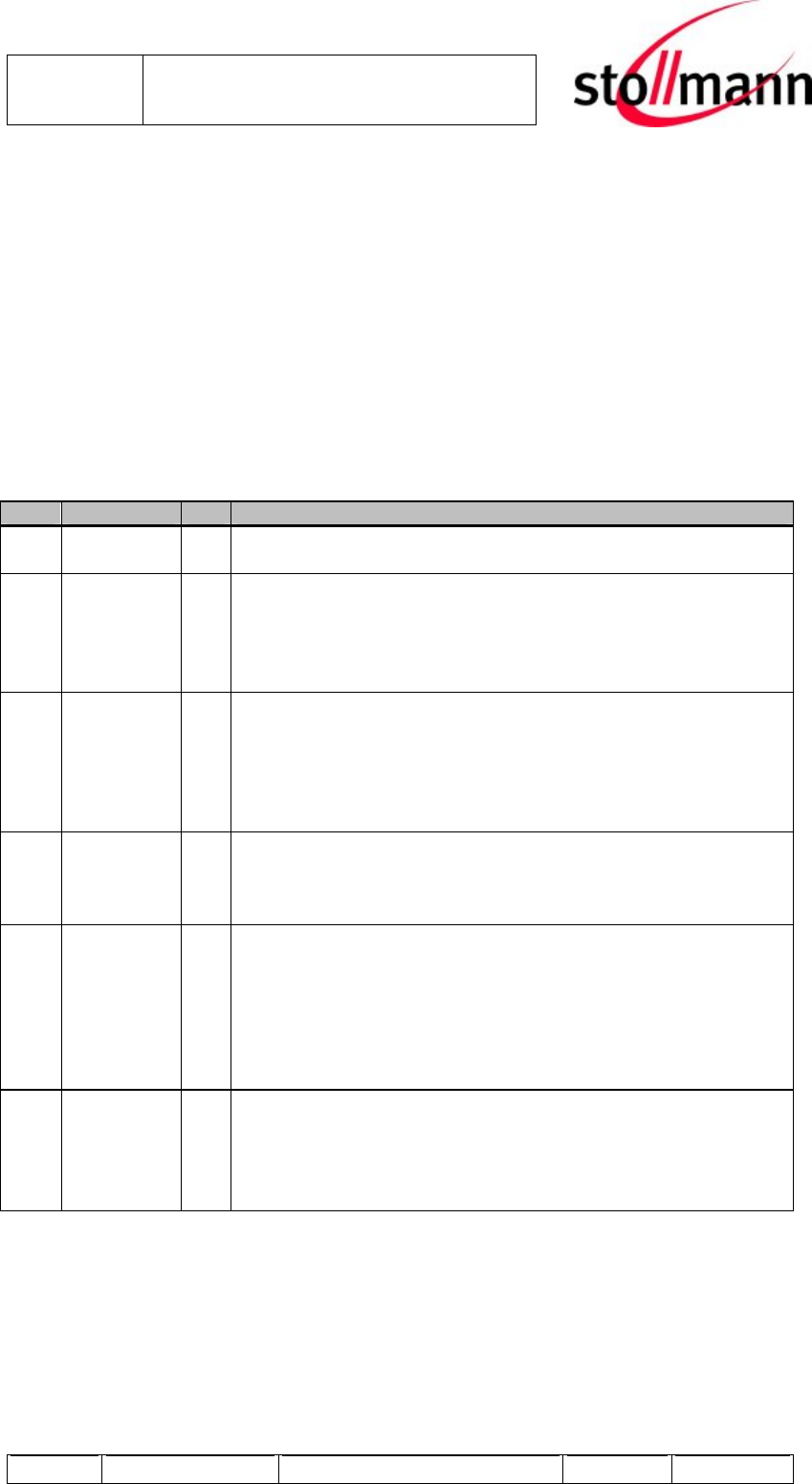
Ver Date by Changes since last Version
1.1 24.05.2005 jw Adopted chap. 5 Terminal Layout to Stollmann Conventions and
Firmware
1.1 26.05.2005 jw Chap. 5 Terminal Layout correct wrong pin type for Pin9 –
GPIO[7]
Correct the mistake for the voltage in chapter Key Features.
Add chapter Ordering Information
Combined with BlueMod+P24
1.2 16.09.2005 jw Enhanced chap. 5.2.1 SPP configuration and 5.2.2
AudioGateway/Headset – SPP configuration
Chapt. 14 Electrical RF-Characteristics sensivity lowered + -85
dBm, all tbd values defined.
Add chap.16.2 For lead-free solder, chap. 18.2 Mass production
status, chap. 20 Reliability Tests, chap. 21 RoHS Declaration
1.3 28.09.2005 jw chap. 5.2.2 AudioGateway/Headset – SPP configuration
corrected definition for pin 22 – GPIO 6
pin B – GPIO 11 and pin C – GPIO 12 functions were
interchanged, corrected
1.4 24.01.2006 jw introduced new pin type pwr
chap 7.5.1 D+, D- added not for unused USB pins
chap 5.1 General Pin Assignment changed pin 15 to reserved
chap 5.2.1 SPP configuration corrected wrong description for
GPIO 1 and GPIO 5
enhanced chap 7.3 Reset
new chap 7.1 Power supply
1.5 31.03.2006 jw added chap 21.2 FCC Compliance
Min VCC reduced to 2.7V
added serial port character representation
added hint on AN_B0601_Antenna_Design
removed HCI specifics from GPIO chapter
Author: jw Date of Saving: 03.04.06 Ref: BlueMod+P2_HW_reference_V1_5.doc Revision: 1.5 Page 35 of 35
