Telit Wireless Solutions MSR Bluetooth Module User Manual Stollmann Dokumentation
Stollmann E+V GmbH Bluetooth Module Stollmann Dokumentation
User Manual
BlueMod+SR/AI
BlueMod+SR/AP
Hardware Reference
Release r04d01

BlueMod+SR/AI
BlueMod+SR/AP
Hardware Reference
Release r04d01 www.stollmann.de Page 2 of 65
Note
This device was developed for the purpose of communication in an office environment. It is
intended solely for our industrial clients for physical integration into their own technical products
after careful examination by experienced technical personnel for its suitability for the intended
purpose. The device was not developed for or intended for use in any specific customer
application. The firmware of the device may have to be adapted to the specific intended modalities
of use or even replaced by other firmware in order to ensure flawless function in the respective
areas of application. Performance data (range, power requirements, etc.) may depend on the
operating environment, the area of application, the configuration, and method of control, as well as
on other conditions of use; these may deviate from the technical specifications, the Design Guide
specifications, or other product documentation. The actual performance characteristics can be
determined only by measurements subsequent to integration. Variations in the performance data of
mass-produced devices may occur due to individual differences between such devices. Device
samples were tested in a reference environment for compliance with the legal requirements
applicable to the reference environment. No representation is made regarding the compliance with
legal, regulatory, or other requirements in other environments. No representation can be made and
no warranty can be assumed regarding the suitability of the device for a specific purpose as
defined by our customers. Stollmann reserves the right to make changes to the hardware or
firmware or to the specifications without prior notice or to replace the device with a successor
model. Of course, any changes to the hardware or firmware of any devices for which we have
entered into a supply agreement with our customers will be made only if, and only to the extent
that, such changes can reasonably be expected to be acceptable to our customers. No general
commitment will be made regarding periods of availability; these must be subject to individual
agreement. All agreements are subject to our Terms and Conditions for Deliveries and Payments,
a copy of which is available from Stollmann.
Copyright © 2013 Stollmann E+V GmbH
Trademarks
The Bluetooth® word mark and logos are owned by the Bluetooth SIG, Inc. and any use of such
marks by Stollmann E+V GmbH is under license. Other trademarks and trade names are those of
their respective owners.

BlueMod+SR/AI
BlueMod+SR/AP
Hardware Reference
Release r04d01 www.stollmann.de Page 3 of 65
Table of contents
1 Introduction .............................................................................................................................. 8
1.1 Feature Summary ............................................................................................................. 8
1.2 Applications ...................................................................................................................... 9
Support for any additional profile is possible on request........................................................... 9
1.2.1 General Cable Replacement ...................................................................................... 9
1.2.2 Industry ...................................................................................................................... 9
1.2.3 Automotive ................................................................................................................. 9
1.2.4 Healthcare and Medical ............................................................................................. 9
1.2.5 Sports and Fitness ................................................................................................... 10
1.2.6 Entertainment .......................................................................................................... 10
2 Block Diagram ....................................................................................................................... 11
3 Application Interface .............................................................................................................. 12
3.1 Power Supply ................................................................................................................. 12
3.2 Power-up / -down Slew-Rate .......................................................................................... 12
3.3 Reset .............................................................................................................................. 13
3.4 Supply Voltage Monitor ................................................................................................... 14
3.5 Serial Interface................................................................................................................ 15
3.5.1 3-Wire Serial Interface ............................................................................................. 16
3.5.2 Baudrate Deviation .................................................................................................. 17
3.6 GPIO Interface ................................................................................................................ 17
3.7 I2C Interface .................................................................................................................... 18
3.8 SPI Serial Peripheral Interface ........................................................................................ 19
3.9 Bluetooth Radio Interface ............................................................................................... 19
3.10 WLAN Coexistence Interface .......................................................................................... 20
3.11 Slow Clock Interface ....................................................................................................... 20
3.12 Test Mode Enable ........................................................................................................... 20
3.13 Pin Strapped System Memory Boot Mode Invocation ..................................................... 21
3.14 Operating in a Power-Switched Environment .................................................................. 21
3.15 Serial Wire Interface ....................................................................................................... 22
4 Module Pins ........................................................................................................................... 22
4.1 Pin Numbering ................................................................................................................ 22

BlueMod+SR/AI
BlueMod+SR/AP
Hardware Reference
Release r04d01 www.stollmann.de Page 4 of 65
4.2 Pin Description................................................................................................................ 23
4.2.1 General Pin Description ........................................................................................... 23
4.2.2 Application Specific Pin Description ......................................................................... 24
4.2.2.1 SPP Pin Configuration .......................................................................................... 24
4.3 Handling of Unused Signals ............................................................................................ 25
5 Electrical Characteristics ........................................................................................................ 27
5.1 Absolute Maximum Ratings ............................................................................................ 27
5.2 Electrical Requirements .................................................................................................. 27
5.3 Operating Conditions ...................................................................................................... 27
5.4 Environmental Requirements .......................................................................................... 28
5.5 Digital I/O Including EXT-RES# ...................................................................................... 28
5.6 Power Consumption and Power Down Modes ................................................................ 31
5.6.1 SPP Configuration ................................................................................................... 31
5.7 RF Performance ............................................................................................................. 33
5.7.1 GFSK, PI/4 DQPSK, 8DPSK Receiver ..................................................................... 33
5.7.2 GFSK, PI/4 DQPSK, 8DPSK Transmitter ................................................................. 36
5.7.3 BLE Receiver ........................................................................................................... 39
5.7.4 BLE Transmitter ....................................................................................................... 40
5.7.5 Antenna-Gain and Radiation Pattern ....................................................................... 42
5.8 Power-Up Time ............................................................................................................... 44
6 Mechanical Characteristics .................................................................................................... 45
6.1 Dimensions ..................................................................................................................... 45
6.2 Recommended Land Pattern .......................................................................................... 46
6.3 Re-flow Temperature-Time Profile .................................................................................. 47
6.4 Placement Recommendation .......................................................................................... 48
6.5 Housing Guidelines ......................................................................................................... 48
6.6 Antenna Issues ............................................................................................................... 48
6.7 Safety Guidelines ............................................................................................................ 49
7 Application Diagram ............................................................................................................... 50
8 Approvals/Certifications ......................................................................................................... 51
8.1 Declaration of Conformity CE .......................................................................................... 51
8.2 FCC Compliance ............................................................................................................ 52

BlueMod+SR/AI
BlueMod+SR/AP
Hardware Reference
Release r04d01 www.stollmann.de Page 5 of 65
8.2.1 FCC Grant ............................................................................................................... 52
8.2.2 FCC Statement ........................................................................................................ 52
8.2.3 FCC Caution ............................................................................................................ 52
8.2.4 FCC Warning ........................................................................................................... 52
8.2.5 FCC RF-exposure Statement ................................................................................... 53
8.2.6 FCC Labeling Requirements for the End Product .................................................... 54
8.3 IC Compliance ................................................................................................................ 55
8.3.1 IC Grant ................................................................................................................... 55
8.3.2 IC Statement ............................................................................................................ 56
8.3.3 IC Caution ................................................................................................................ 56
8.3.4 IC RF-exposure Statement ...................................................................................... 56
8.3.5 IC Labeling Requirements for the End Product ........................................................ 57
8.3.6 IC Label Information BlueMod+SR ........................................................................... 57
8.4 Bluetooth Qualification .................................................................................................... 58
8.5 RoHS Declaration ........................................................................................................... 59
9 Related Documents ............................................................................................................... 59
10 Packing ............................................................................................................................... 60
10.1 Tape ............................................................................................................................... 61
10.2 Reel ................................................................................................................................ 61
10.3 Package Label ................................................................................................................ 62
11 Ordering Information ........................................................................................................... 63
11.1 Part Numbers.................................................................................................................. 63
11.2 Standard Packing Unit .................................................................................................... 63
11.3 Evaluation Kit .................................................................................................................. 63
12 History ................................................................................................................................. 64
List of Figures
Figure 1: BlueMod+SR Block Diagram .......................................................................................... 11
Figure 2: BlueMod+SR Example Power Supply ............................................................................ 12
Figure 3: BlueMod+SR Example Reset ......................................................................................... 13
Figure 4: Serial Interface Signals .................................................................................................. 15
Figure 5: BlueMod+SR Example Serial Interface (RS-232) Supporting UICP ............................... 16

BlueMod+SR/AI
BlueMod+SR/AP
Hardware Reference
Release r04d01 www.stollmann.de Page 6 of 65
Figure 6: BlueMod+SR Example Serial Interface (Mixed Signal Level) ......................................... 17
Figure 7: BlueMod+SR I2C Interface ............................................................................................. 18
Figure 9: Unity 3e+ Coexistence ................................................................................................... 20
Figure 10: BlueMod+SR Pin Numbering (Top View) ..................................................................... 22
Figure 12: Typical Antenna Radiation Pattern at 2441MHz ........................................................... 43
Figure 13: Typical Antenna Radiation Pattern at 2480MHz ........................................................... 43
Figure 14: BlueMod+SR/AI dimensions......................................................................................... 45
Figure 15: BlueMod+SR/AP Dimensions ....................................................................................... 45
Figure 16: BlueMod+SR Land Pattern .......................................................................................... 46
Figure 17: Soldering Temperature-Time Profile (For Reflow Soldering) ........................................ 47
Figure 18: BlueMod+SR/AI Placement Recommendation ............................................................. 48
Figure 19: Typical Application Schematics .................................................................................... 50
List of Tables
Table 1: Power up/down Slew Rate Requirements ....................................................................... 12
Table 2: Pin States during Reset ................................................................................................... 14
Table 3: Baudrates and Deviations ............................................................................................... 17
Table 4: General Pin Assignment .................................................................................................. 23
Table 5: Application Specific Pin Assignments, SPP ..................................................................... 25
Table 6: Absolute Maximum Ratings ............................................................................................. 27
Table 7: Electrical Requirements .................................................................................................. 27
Table 8: DC Operating Conditions ................................................................................................ 27
Table 9: Environmental Requirements .......................................................................................... 28
Table 10: DC Characteristics, Digital IO (STM32-related) ............................................................. 29
Table 11: DC Characteristics, SLCK (STM32 Backup Domain) ..................................................... 30
Table 12: DC Characteristics, Digital IO (CSR8811 Related) ........................................................ 30
Table 13: Supply Current SPP Standby Modes no Radio Activity ................................................. 31
Table 14: Supply Current, SPP Bluetooth Classic ......................................................................... 31
Table 15: Supply Current BLE Peripheral Device Role ................................................................. 32
Table 16: RF Performance GFSK, PI/4 DQPSK, 8DPSK Receiver ............................................... 35

BlueMod+SR/AI
BlueMod+SR/AP
Hardware Reference
Release r04d01 www.stollmann.de Page 7 of 65
Table 17: RF Performance GFSK, PI/4 DQPSK, 8DPSK Transmitter ........................................... 38
Table 18: RF Performance BLE Receiver ..................................................................................... 39
Table 19: RF Performance BLE Transmitter ................................................................................. 41

BlueMod+SR/AI
BlueMod+SR/AP
Hardware Reference
Release r04d01 www.stollmann.de Page 8 of 65
1 Introduction
This Hardware Reference documents how the BlueMod+SR/AI and BlueMod+SR/AP can be
integrated into customer systems. It addresses hardware specifications of the BlueMod+SR/AI and
/AP and requirements of the hardware environments for the BlueMod+SR/AI and BlueMod+SR/AP.
Notation: The term BlueMod+SR refers to both the BlueMod+SR/AI and the BlueMod+SR/AP.
For detailed information about software interfaces refer to [5]
For the latest version of this document please check the following URL:
http://www.stollmann.de/en/support/downloads/bluetooth-adapter/bluemod-sr.html
1.1 Feature Summary
• Bluetooth specification V4.0 compliant
• Supports BR/EDR/LE
• Supports Dual Mode
• Fully qualified Bluetooth V4.0 Dual Mode BR/EDR/LE
• CE certified
• FCC and IC certified
• CSR8811 BlueCore08 and Application Processor inside
• Complete Co-location and Co-existence with 802.11 (AFH, Unity 3e+)
• Fast Connection Setup
• RF output power up to +7dBm with power control
• Supply Voltage range 2,5V to 3,6V, typical 3.3V
• Internal crystal oscillator (26 MHz and 14,7456 MHz)
• LGA Surface mount type: BlueMod+SR: 17 x 10 x 2.6 mm3
• Shielded to be compliant to FCC full modular approval
• Bluetooth enhanced data rate up to 2178kbps asymmetric
• Support for all Bluetooth power saving modes (Park, Sniff, Hold)
• Optional support for ultra-low-power mode
• Full 8- to 128-bit encryption
• High sensitivity design
• High-speed UART interface
• I2C interface
• SPI interface
• Up to 11 digital IO’s for individual usage by embedded software
• Cortex-M3 STM32F103 core for embedded profiles or application software
• Manufactured in conformance with RoHS2
• Operating temperature -30 ... +85 °C

BlueMod+SR/AI
BlueMod+SR/AP
Hardware Reference
Release r04d01 www.stollmann.de Page 9 of 65
1.2 Applications
The BlueMod+SR can be used in different applications. Regardless if the application requires high
throughput or low energy consumption, BlueMod+SR offers the best of both worlds. Some typical
applications are described in this chapter.
Supported profiles are:
BR/EDR:
• SPP
LE:
• Terminal IO
• any GATT based LE-profile
Support for any additional profile is possible on request.
1.2.1 General Cable Replacement
The Serial Port Profile (SPP) on the BlueMod+SR can be used for UART data transfer. The
connection is transparent for the user application and supports Secure Simple Pairing, making the
pairing process easy and the connection secure.
1.2.2 Industry
Typical Bluetooth application include scanner, printer as well as automation controls. In the
automation application area Bluetooth is mainly used for transport of I/O signals. Bluetooth low
energy can be used to monitor and control motors, actuators, values and entire processes.
1.2.3 Automotive
Modules are mainly used in aftermarket application like personal navigation devices, head units or
audio applications. These applications are typically Bluetooth BR/EDR only.
1.2.4 Healthcare and Medical
The healthcare and medical market offers a lot of possible application for Bluetooth BR/EDR and
Bluetooth Low Energy. Usage of Bluetooth is aimed mainly at devices that are used for monitoring
vital data. Typical devices are blood glucose meter, blood pressure cuffs and pulse ox meters.
Bluetooth BR/EDR and low energy were chosen by the Continua Health Alliance as transports for
interoperable end to end communication.

BlueMod+SR/AI
BlueMod+SR/AP
Hardware Reference
Release r04d01 www.stollmann.de Page 10 of 65
1.2.5 Sports and Fitness
In the sports and fitness segment Bluetooth is used in devices for positioning as well as monitoring
vital data. Typical devices in this market are heart rate monitors, body temperature thermometers,
pedometers, cadence meters, altimeter, positioning / GPS tracking and watches displaying
information from sensors.
1.2.6 Entertainment
Bluetooth technology is already used in a wide variety of devices in the entertainment sector,
namely set-top boxes / gaming consoles. Bluetooth low energy is expected to further increase the
use of Bluetooth technology in devices like TV / DVD / STB / Media Player, remote controls,
gaming controller, wireless mouse/keyboard.
BlueMod+SR/AI
BlueMod+SR/AP
Hardware Reference
Release r04d01 www.stollmann.de Page 11 of 65
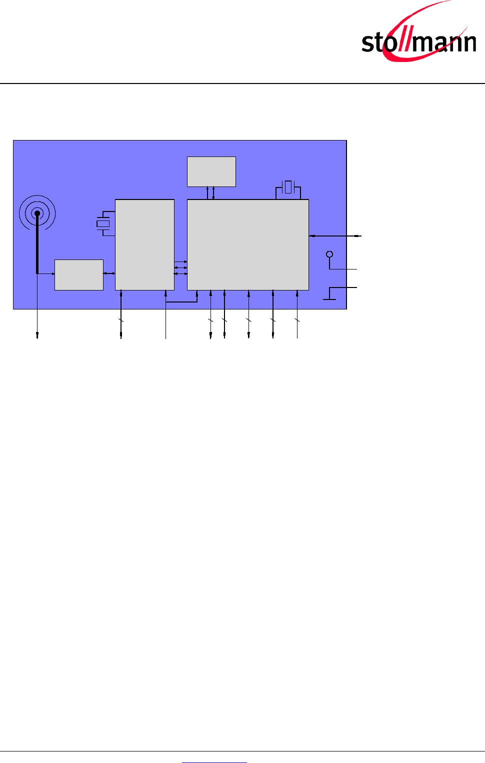
2 Block Diagram
STM32F103
CSR8811
VSUP
BlueMod+SR
BP
Filter
RESET
I2C
UART
GPIO
SPI
WLAN-COEX
1
2
7
3
4
GND
3.3V
26MHz
14,7456MHz
opt. 32kHz
9
EEPROM
DEBUG
onboard
antenna
EXT-ANT
1)
2)
1) BlueMod+SR/AI only
2)BlueMod+SR/AP only
Figure 1: BlueMod+SR Block Diagram
Note:
BlueMod+SR/AI has an internal ceramic antenna whereas BlueMod+SR/AP provides for an 50Ω
RF interface
BlueMod+SR/AI
BlueMod+SR/AP
Hardware Reference
Release r04d01 www.stollmann.de Page 12 of 65
3 Application Interface
3.1 Power Supply
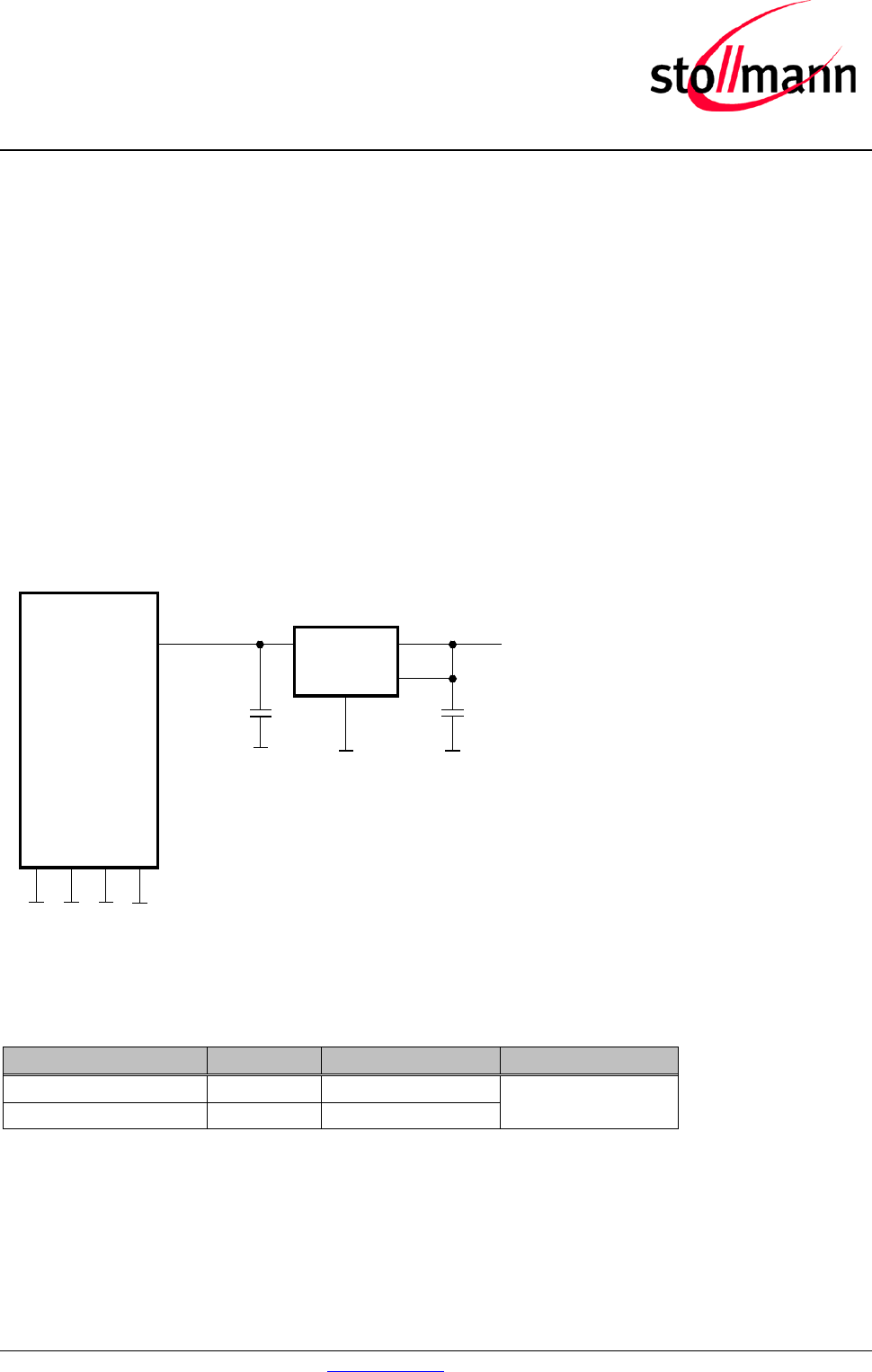
BlueMod+SR require a power supply with the following characteristics:
Typical: 3,3VDC, min.: 2,5VDC, max.: 3.6VDC, low noise (≤ 10mVrms), > 80mA peak
For optimal performance a stable supply is recommended. If a regulator is to be used, it should be
a fast linear regulator placed as close as possible to the VSUP pins (E-6, F-6). Functionality has
been verified with the following types: TOREX: XC6204x332xx or XC6401xx42xx.
If the regulator cannot be placed close to the BlueMod+SR, it is recommended to place an
additional low ESR capacitor with at least 10µF as close as possible to the VSUP pins (E-6, F-6 or
C-1).
BlueMod+SR
XC6204-3.3
C-1,E-6,F-6
VSUP
GND:
A-7,E-7,F-7,B-[5:8],
C-[5:8],D-8,E-8,F-8
10µ + 100n + 1n
1µ
VOUT
VSS
VIN
CE
5 1
3
2
+5VDC
Figure 2: BlueMod+SR Example Power Supply
3.2 Power-up / -down Slew-Rate
Parameter
Min
Max
Unit
VSUP rise time rate 0 ∞ µs/V
VSUP fall time rate 20 ∞
Table 1: Power up/down Slew Rate Requirements
BlueMod+SR/AI
BlueMod+SR/AP
Hardware Reference
Release r04d01 www.stollmann.de Page 13 of 65
3.3 Reset
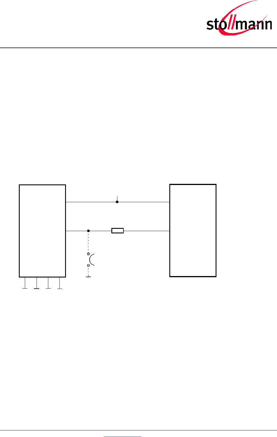
BlueMod+SR are equipped with circuitry for generating Power ON Reset from the internal core
voltage. A reset is generated when the core voltage falls below typically 1,88V and is released
when it rises above typically 1,92V.
By holding pin B-1 (EXT-RES#) at ≤ 0,5V for ≥ 5ms, an external reset is generated. This pin has a
fixed internal pull-up resistor (RPU = 30kΩ ... 50kΩ) and a capacitor to GND (100n) which acts as
debounce filter. If EXT-RES# is not used, it may be left open.
Note:
EXT-RES# pin can also be output. Use an open drain device or push button to drive it low. EXT-
RES# must not be connected to VSUP or driven to logic high-level directly. Provide for an 1kΩ
series resistor when driving EXT-RES# from a CMOS output.
BlueMod+SR
C-1,E-6,F-6
VSUP
GND
+3V3
EXT-RES# B-1
Reset-Switch is optional
Please Note: BlueMod+SR has an open-drain output and approx. 40k internal pullup
1k
Reset signal is optional
Host MCU
GPIO
VDD
Figure 3: BlueMod+SR Example Reset
BlueMod+SR/AI
BlueMod+SR/AP
Hardware Reference
Release r04d01 www.stollmann.de Page 14 of 65
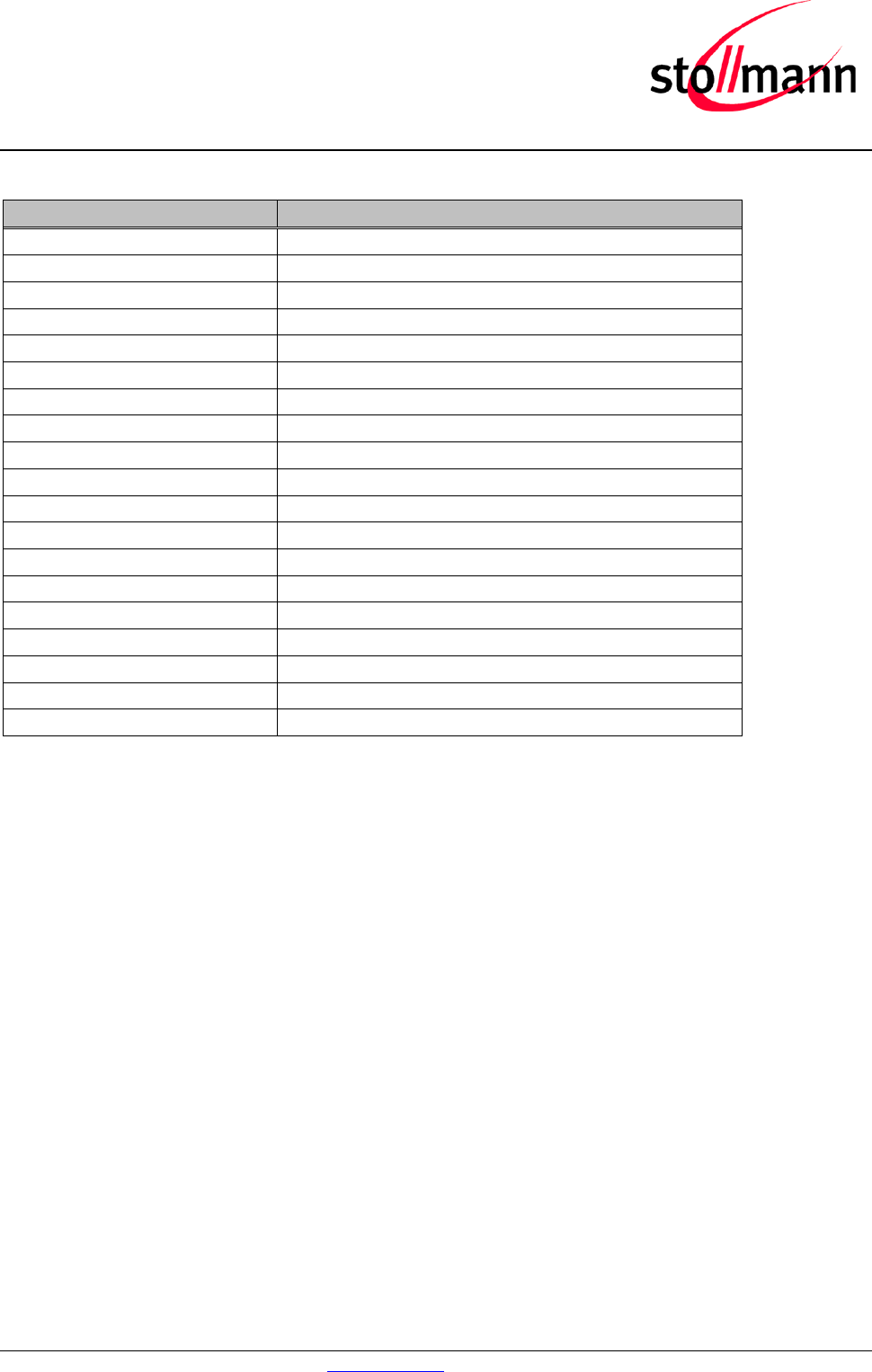
The following table shows the pin states of BlueMod+SR during reset active.
Pin Name State: BlueMod+SR
EXT-RES# I/O with pull-up
(1)
and 100n to GND – use open drain
SLCK Input with weak pull-down
(2)
UART-TXD Input floating
UART-RXD Input floating
UART-RTS# Input with pull-up resistor 470kΩ
(4)
UART-CTS# Input floating
IUR-OUT# Input with pull-up resistor 470kΩ
(4)
IUR-IN# Input floating
GPIO[0:4, 6:7] Input floating
GPIO[5] Input with pull-up
(1)
GPIO[8] Output (JTDO)
BT-ACT Input with weak pull-up
(2)
BT-STAT Input with weak pull-up
(2)
WLAN-DNY Input with weak pull-up
(2)
BT-PER Input with weak pull-up
(2)
TESTMODE# Input floating
BOOT0 Input with pull-down resistor 100kΩ
(4)
SWDIO Input with pull-up
(1)
SWCLK Input with pull-down
(1)
(1) pull-up, pull-down: RPU, RPD is typ. 40kΩ (30kΩ to 50kΩ)
(2) weak pull-up, pull-down: See Table 12: DC characteristics, digital IO (CSR8811 related)
(3) strong pull-up, pull-down: See Table 12: DC characteristics, digital IO (CSR8811 related)
(4)
a discrete resistor is used
Table 2: Pin States during Reset
The pin states as indicated in Table 2 are kept until hardware initialization has started.
3.4 Supply Voltage Monitor
Supply-under-voltage detection is implemented using the STM32 embedded supply voltage
monitor PVD. When VSUP falls below a threshold VPVD (programmed to 2,38V ± 0,1V), a system
reset will be asserted.
BlueMod+SR/AI
BlueMod+SR/AP
Hardware Reference
Release r04d01 www.stollmann.de Page 15 of 65
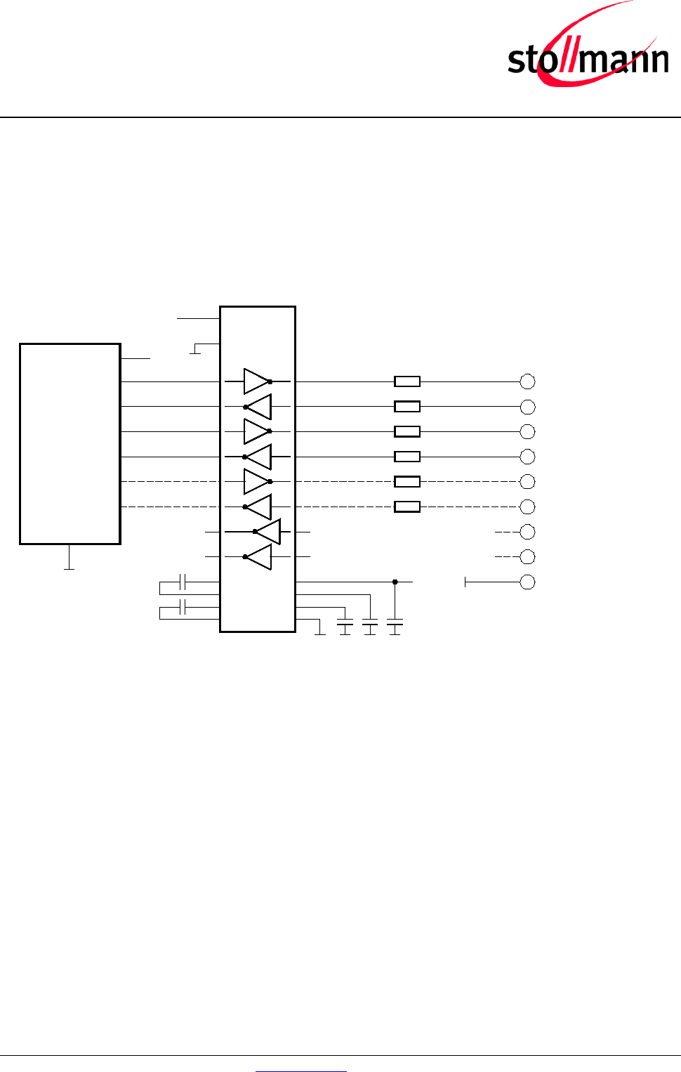
3.5 Serial Interface
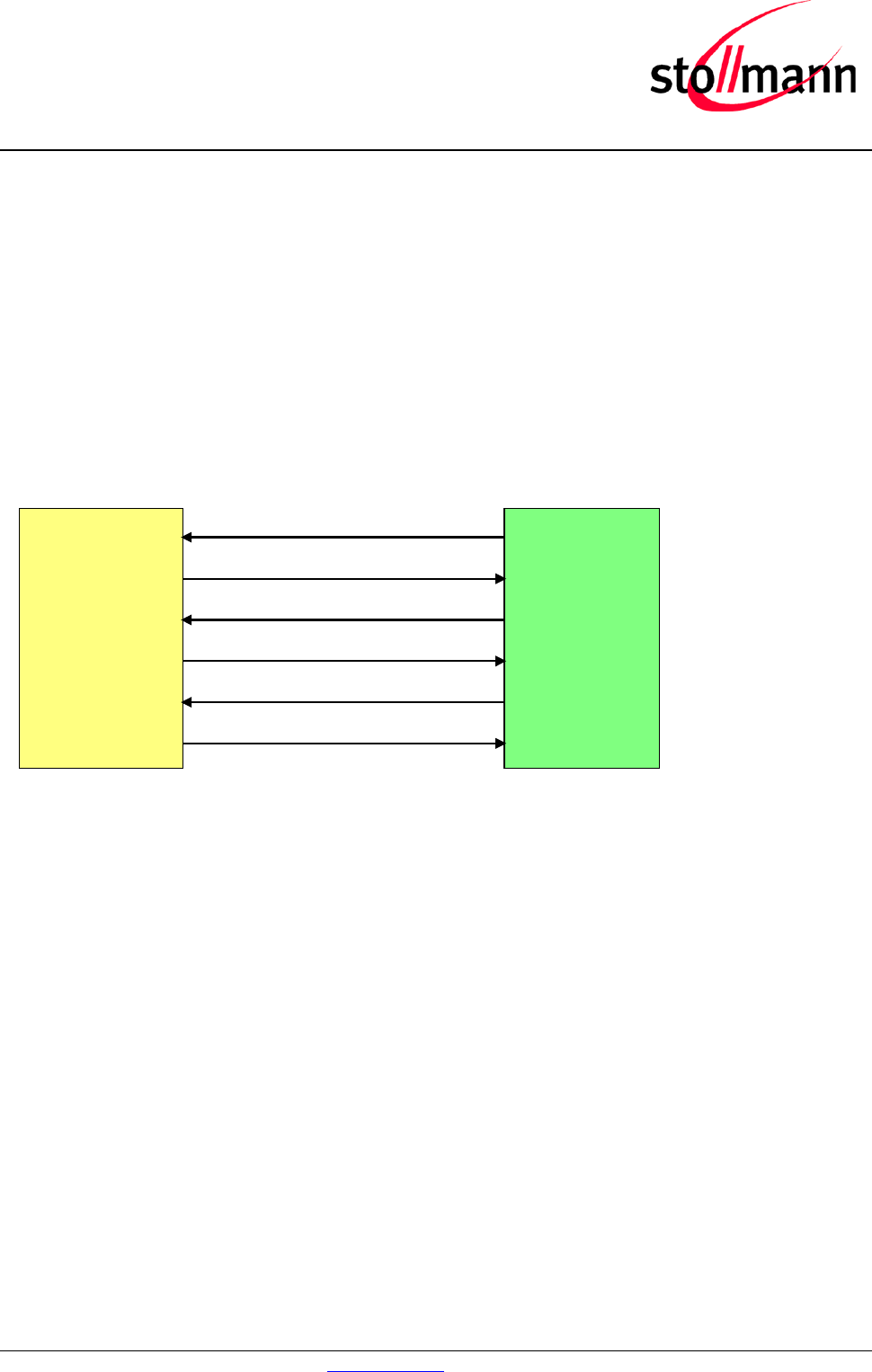
The serial interface of BlueMod+SR is a high-speed UART interface supporting RTS/CTS flow
control and interface-up/down mechanism according to the UICP+ protocol (refer to [3] ). Electrical
interfacing is at CMOS levels (defined by VSUP).
• Transmission speeds are 9600 – 921600 bps (asynchronous)
• Character representation: 8 Bit, no parity, 1 stop bit
• Hardware flow-control with RTS and CTS (active low)
Note: Transmission speed may be limited by firmware. See corresponding command reference
[5] for further information.
BlueMod+SR
Host
UART-RXD
UART-TXD
UART-CTS#
UART-RTS#
IUR-IN#
IUR-OUT#
Figure 4: Serial Interface Signals
The basic serial interface (with RTS/CTS flow control) uses only four signal lines (UART-RXD,
UART-TXD, UART-CTS#, UART-RTS#). IUR-IN#, IUR-OUT# and GPIO[4] (see below) can be left
unconnected.
A substantially saving of power during idle phases can be achieved (see 5.6.1) when the UICP
protocol is used (refer to [3] ). This protocol has to be complemented on the host side as well.
Signals IUR-IN# and IUR-OUT# should be connected to the host and may be mapped to DSR and
DTR, if an RS232-style (DTE-type) interface is used (see Figure 5).
When using the SPP firmware and applications, call control can be supported by GPIO[4]. Driving
GPIO[4] to logic High level during a data transfer phase will “hang up” the connection and
disconnect the Bluetooth link. This signal may be mapped to DSR, if an RS232-style (DTE-type)
interface is used. Please refer to [5] for a functional specification. GPIO[4] can be left unconnected
if this feature is not used.
BlueMod+SR/AI
BlueMod+SR/AP
Hardware Reference
Release r04d01 www.stollmann.de Page 16 of 65
3.5.1 3-Wire Serial Interface
When using only GND and UART-RXD, UART-TXD serial lines, leave UART-RTS# and UART-
CTS# open
Note: It is strongly recommended to use hardware flow control. Not using flow control can cause
a loss of data.
2
BlueMod+SR
GND
MAX3241
14
+3V3
22
23
2
3
7
8
4
6
1
9
TXD
RXD
RTS#
CTS#
IUR-OUT#
IUR-IN#
TXD
RXD
RTS
CTS
DTR
DSR
DCD
RI
RS232
DSUB9 (male)
DTE style connector
9
4
10
5
11
6
7
8
19
13
18
12
17
16
15
F-4
D-2
D-7
F-3
B-4
D-5
UART_TXD
UART_RXD
UART_RTS#
UART_CTS#
IUR-OUT#
IUR-IN#
SHDN#
EN#
100n
100n
28
24
1
+3V3
100n 100n 100n
26
3
27
25
V+
VCC
V -
GND
C2+
C2-
C1+
C1-
220R
220R
220R
220R
220R
220R
5
SigGND
can be left open
VSUP
+3V3
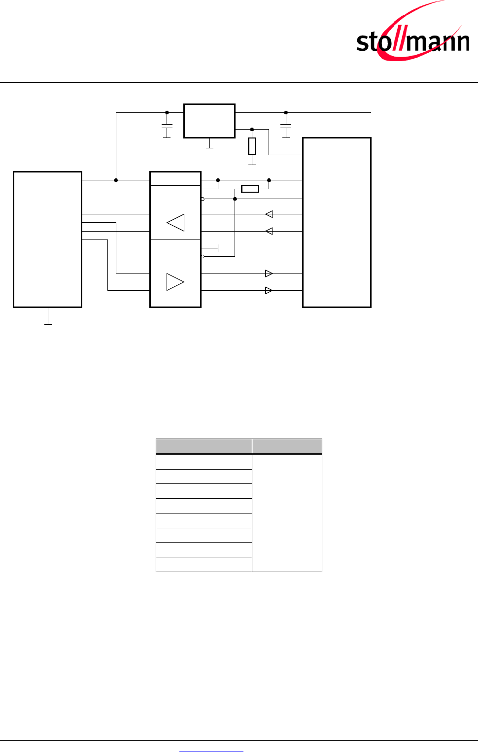
Figure 5: BlueMod+SR Example Serial Interface (RS-232) Supporting UICP
BlueMod+SR/AI
BlueMod+SR/AP
Hardware Reference
Release r04d01 www.stollmann.de Page 17 of 65
VDDIO
(+1.2V .. +3.6V)
BlueMod+SR
GND
D-2
F-4
F-3
D-7
UART_RXD
UART_TXD
UART_CTS#
UART_RTS#
10µ+100n+1n
SN74AVC4T245
User Host System
VSUP
XC6204-3.3
VOUT
VSS
VIN
CE 1µ
100k
100k
VCCB
1B1
1B2
2B1
2B2 2A2
2A1
1A2
1A1
VCCA
1DIR
1OE
2DIR
2OE
(GPIO, Out,
no pu/pd)
(GPIO, Out,
no pu/pd)
TXD
RTS#
RXD
CTS#
+5VDC
OE_DRV#
BT_ENABLE
VDD_HOST (+1.2 .. +3.6V)
+3V3_switched
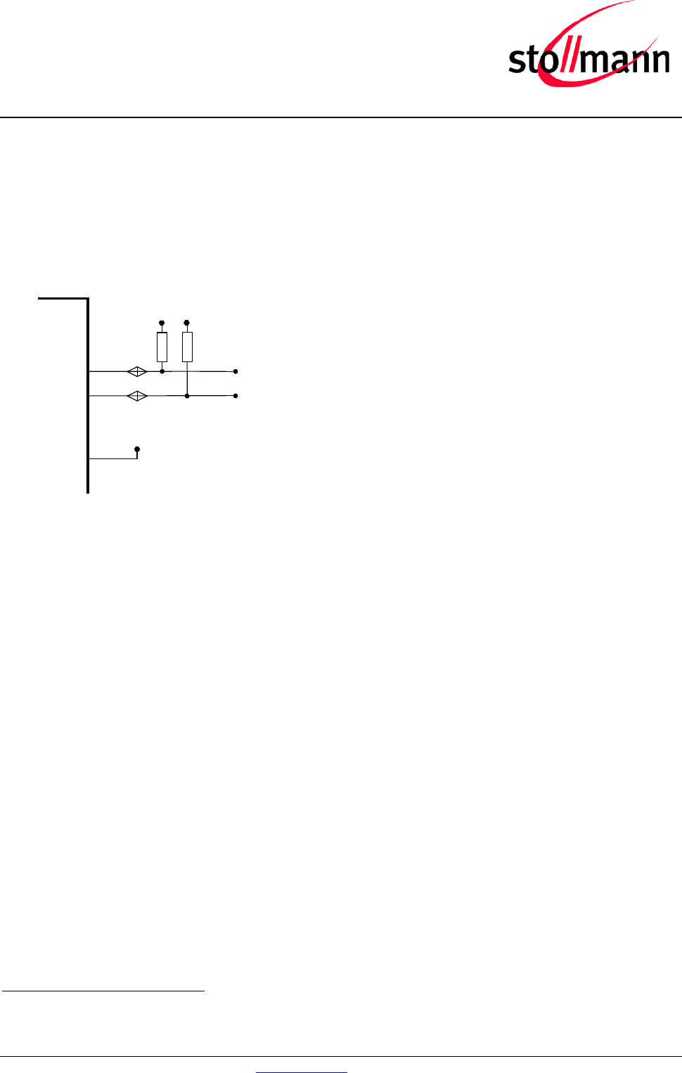
Figure 6: BlueMod+SR Example Serial Interface (Mixed Signal Level)
3.5.2 Baudrate Deviation
The following table shows the deviation in percent of the standard data rates. The deviation may
be caused by the inaccuracy of the crystal oscillator or granularity of the baud rate generator.
Data Rate (bits/s) Deviation (%)
9600
±1%
19200
38400
57600
115200
230400
460800
921600
Table 3: Baudrates and Deviations
Note: The total deviation of sender and receiver shall not exceed 2.5 % to prevent loss of data.
3.6 GPIO Interface
It is possible to use the programmable digital I/Os GPIO[0:8] on the BlueMod+SR. Their behavior
has to be defined project specific in the firmware.
Unused GPIO pins can be left unconnected.
BlueMod+SR/AI
BlueMod+SR/AP
Hardware Reference
Release r04d01 www.stollmann.de Page 18 of 65
3.7 I2C Interface1
The I2C bus interface serves as an interface between the internal microcontroller and the serial I2C
bus. It provides multimaster capability, and controls all I2C bus specific sequencing, protocol,
arbitration and timing. It supports standard (100kHz) and fast (400kHz) speed modes.
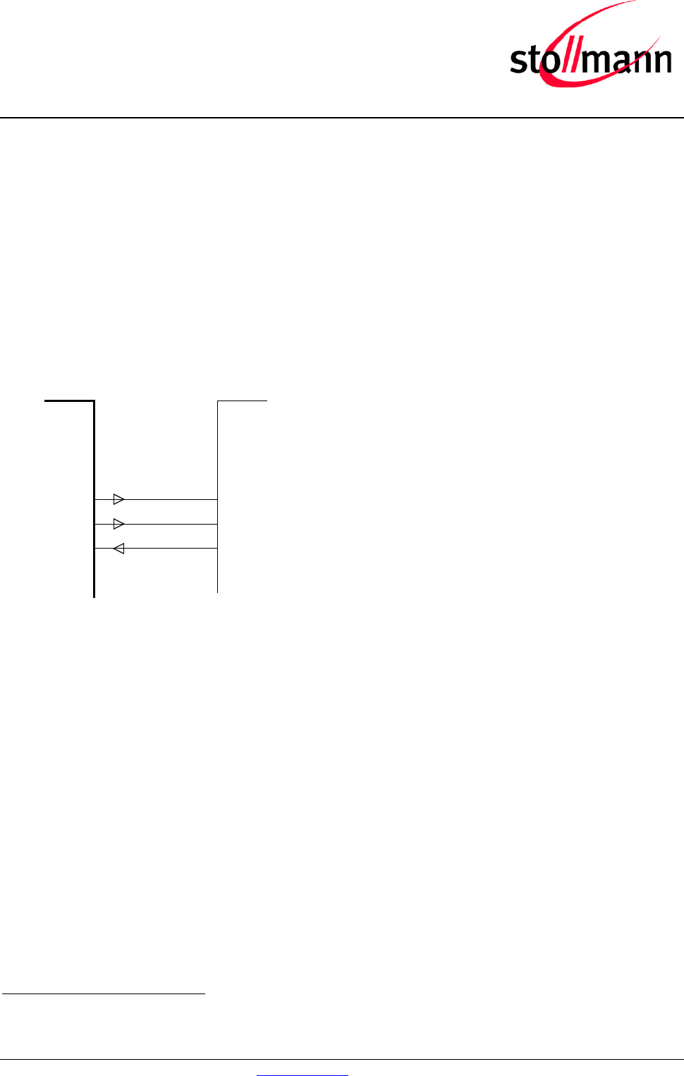
GPIO[1]/I2C-SDA and GPIO[0]/I2C-SCL can be used to form an I2C interface. It is required to
connect 4k7 pull-up resistors on I2C-SCL and I2C-SDA when this interface is used.
I2C-SCL
I2C-SDA
GPIO[0]/I2C-SCL
GPIO[1]/I2C-SDA
BlueMod+SR
VSUP
Rpu
4k7
+3.3V
B-2
D-3
C-1,E-6,F-6
+3.3V
Rpu
4k7
+3.3V
Figure 7: BlueMod+SR I2C Interface
1 subject to firmware support, contact Stollmann for current status
BlueMod+SR/AI
BlueMod+SR/AP
Hardware Reference
Release r04d01 www.stollmann.de Page 19 of 65
3.8 SPI Serial Peripheral Interface2
The serial peripheral interface (SPI) allows half/full-duplex, synchronous, serial communication with
external devices. The interface can be configured as the master and in this case it provides the
communication clock (SCK) to the external slave device. The interface is also capable of operating
in multi master configuration. It may be used for a variety of purposes, including simplex
synchronous transfer on two lines with a possible bidirectional data line or reliable communication
using CRC checking. Module pins are used as follows:
• GPIO[2]: SPI-MOSI
• GPIO[5]: SPI-MISO
• GPIO[8]: SPI-SCK
GPIO[8]/SPI-SCK
GPIO[2]/SPI-MOSI
BlueMod+SR
E-2
SPI-Master
Host
SPI-Slave
GPIO[5]/SPI-MISO
D-1
F-2
SCK, SPI_CLK
SDI, MOSI
SDO, MISO
typical signals:
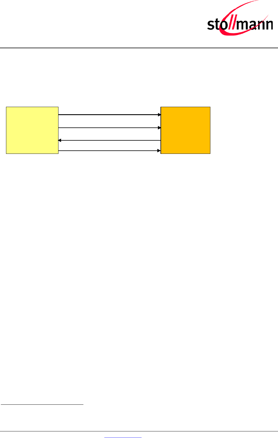
Figure 8: BlueMod+SR SPI Interface e.g. in Master Mode
3.9 Bluetooth Radio Interface
• The BlueMod+SR/AI presents an integrated ceramic antenna.
• The BlueMod+SR/AP presents no integrated ceramic antenna whereas provides a 50Ω RF
interface.
It is highly recommended that you follow the design rule given in the Stollmann Application Note on
Antenna design [4].
2 subject to firmware support, contact Stollmann for current status
BlueMod+SR/AI
BlueMod+SR/AP
Hardware Reference
Release r04d01 www.stollmann.de Page 20 of 65
3.10 WLAN Coexistence Interface3
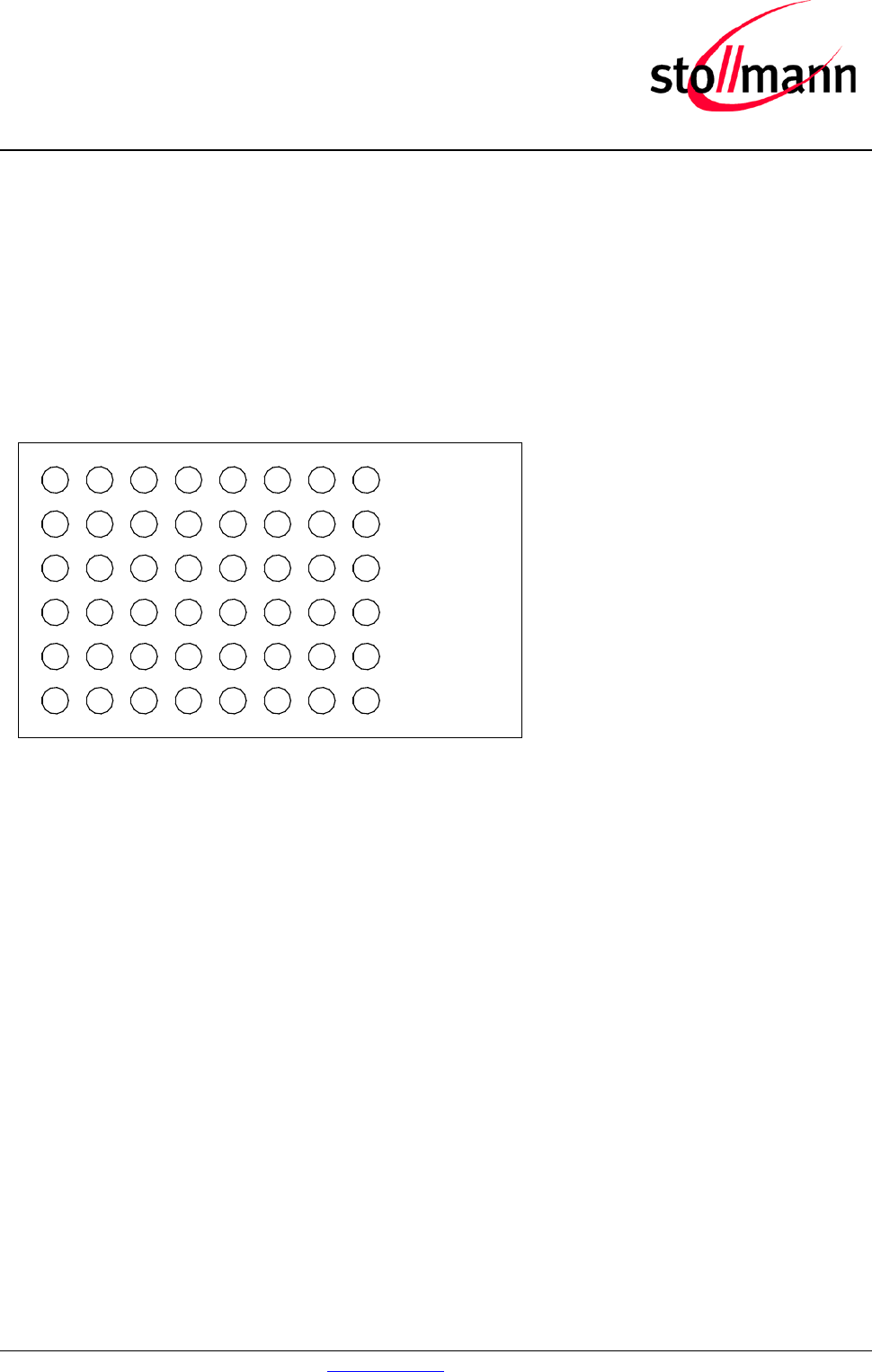
For implementing WLAN Coexistence with CSR’s Wi-Fi solution the Unity 3e+ solution is
implemented. For non-CSR WiFi solutions only the 3 Signals BT_ACTIVE (BT-ACT), BT_STATUS
(BT-STAT) and WLAN_DENY (WLAN-DNY) are used.
BlueMod+SR
WiFi Device
BT-ACT
BT-STAT
WLAN-DNY
BT-PER
Figure 9: Unity 3e+ Coexistence
If this interface is not used, these signals may be left unconnected.
If your application needs to use these signals, ask Stollmann for support.
3.11 Slow Clock Interface
Consumption of power during power-down modes can be reduced by feeding the module with a
32,768 kHz slow clock at pin SLCK.
SLCK specification:
• 32,768 kHz typ., 30 kHz min., 35 kHz max. Duty cycle 30...70%.
• Signal must be square wave, at VSUP-level (see note below) and present as long as VSUP
is powered.
The module’s firmware will detect the presence of a slow clock during the boot process and switch
behavior appropriately. This check does only apply for presence of some clock; it is not checked if
the clock frequency is in the valid range required by CSR8811 (30kHz ... 35kHz).
If this signal is not used, to minimize risk of erroneous pulse detection in noisy environments,
Stollmann recommends the connection of A-6 to GND (direct connection or pull-down resistor).
Note: Since SLCK is fed to both the STM32 and the CSR8811, the electrical characteristics as
described in Table 11 (VLSEH) and Table 12 (VIH) apply at the same time.
3.12 Test Mode Enable
This functionality is reserved. Leave pin TESTMODE# open.
3 subject to firmware support, contact Stollmann for current status

BlueMod+SR/AI
BlueMod+SR/AP
Hardware Reference
Release r04d01 www.stollmann.de Page 21 of 65
3.13 Pin Strapped System Memory Boot Mode Invocation
Asserting BOOT0 “high” will invoke the system memory bootloader at start-up. This is required for
firmware update. Thus, access to this signal and a means to drive it at high level should be
foreseen by the customer’s hardware. While not in use, this signal can be left open or driven to
logic low level.
To connect to the module during system memory boot mode, an RS232 serial interface has to be
directly linked to the UART-TXD (F-4) and UART_RXD (D-2) pins.
The bootloader is stored in the internal boot ROM memory (system memory) of MCU. It is
programmed during production. Its main task is to upgrade the firmware to the internal Flash
memory. A communication protocol is defined with a specific command set and sequences.
The firmware upgrade will be done by either
- a Stollmann provided firmware update tool. This is a Windows program that contains the
firmware and uses a PC with a serial port for the update
- implementing the system memory boot mode protocol on the host system.
If firmware update shall be performed from a host MCU, signals BOOT0 and EXT-RES# both must
be controlled by that host MCU (GPIO ports). Please note that EXT-RES# must not be driven
directly from a push-pull signal (see chapter 3.3).
3.14 Operating in a Power-Switched Environment
A potential "back feeding" problem may arise, if the module is operated in an environment where
its power supply (VSUP) is switched off by the application. This might be done to save some power
in times Bluetooth is not needed.
As stated in Table 6, the voltage on any I/O pin must not exceed VSUP by more than 0,4V at any
time. Otherwise some current IINJECT flows through the internal protection diodes. This may damage
the module.
There is no problem if the application circuit design and programming can assure that all signals
directed towards BlueMod+SR are set to low (U < 0,3V) before and while VSUP is turned off. If this
is not guaranteed, at least a series resistor (about 1k) must be inserted into the signal path. This
does protect the module but obviously cannot prevent from an unwanted, additional current flow in
case of such signal being at high-level. It may be necessary to use driver chips in such
applications, that gate off these signals while VSUP is not present.
BlueMod+SR/AI
BlueMod+SR/AP
Hardware Reference
Release r04d01 www.stollmann.de Page 22 of 65
3.15 Serial Wire Interface
The Serial Wire interface SWDIO, SWCLK is normally not used in a customer’s product. It is
reserved for debugging purposes.
Leave SWDIO, SWCLK unconnected. Only if you intend to use it for debugging purposes, make it
available and connect SWDIO via a pullup resistor 100kΩ to VSUP (refer to [1]).
4 Module Pins
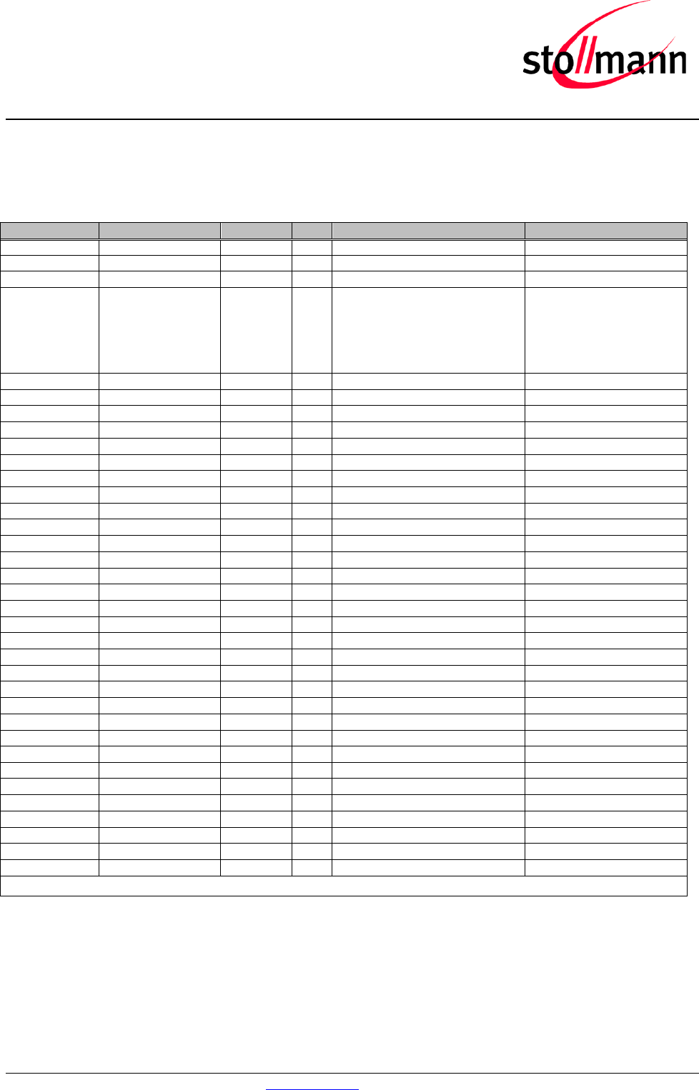
4.1 Pin Numbering
F1
E1
D1
C1
B1
A1 A2 A3 A4 A5 A6 A7 A8
F2
E2
D2
C2
B2
F3
E3
D3
C3
B3
F4
E4
D4
C4
B4
F5
E5
D5
C5
B5
F6
E6
D6
C6
B6
F7
E7
D7
C7
B7
F8
E8
D8
C8
B8
Figure 10: BlueMod+SR Pin Numbering (Top View)
BlueMod+SR/AI
BlueMod+SR/AP
Hardware Reference
Release r04d01 www.stollmann.de Page 23 of 65
4.2 Pin Description
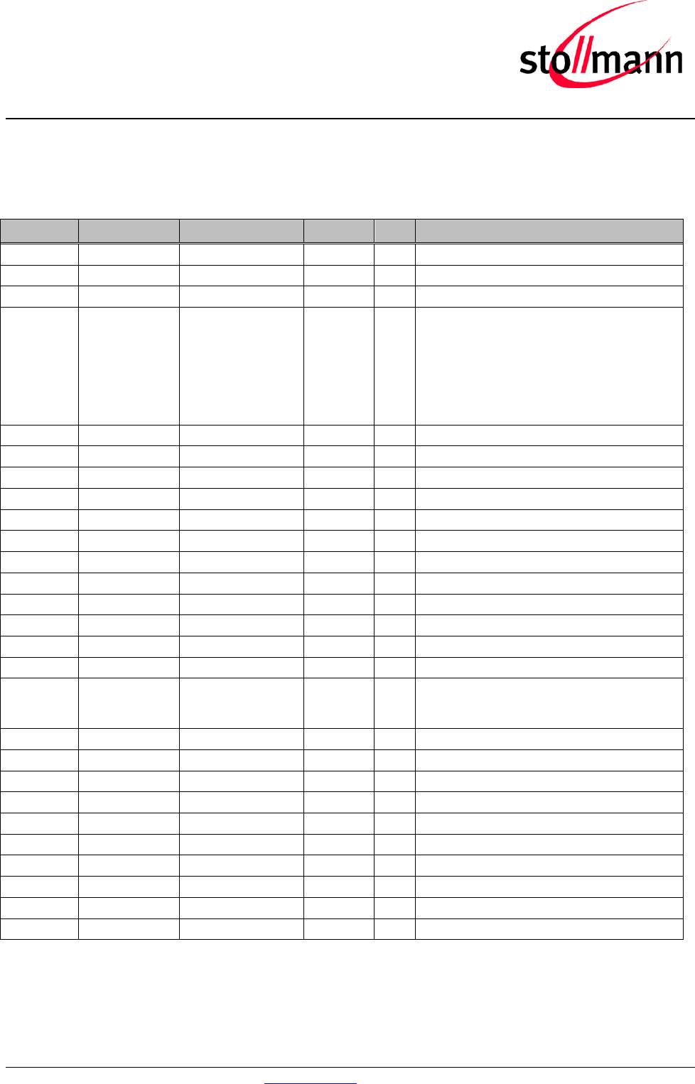
4.2.1 General Pin Description
Type: PU - pull-up; PD – pull-down; PWR – Power; I – Input; O – Output; I/O – bidir.; OD – open drain; PP – push/pull; RF: RadioFreq
Pin Name
Signal
Type
Act
Function
Alternate Function
E-6
VSUP1
PWR
+3,3V nom.
F-6
VSUP2
PWR
+3,3V nom
C-1
VSUP3
PWR
+3,3V nom
A-7, E-7, F-7,
B-[5,6,7,8],
C-[5,6,7,8],
D-8, E-8, F-8
GND PWR Ground
A-8
ANT
RF
n.c. (AI-Variant)
RF (AP-Variant)
B-1
EXT-RES#
I/O-PU
L
User Reset
A-6
SLCK
I-PD
32kHz Slow Clock
F-4
UART-TXD
O-PP
IUR Data OUT
D-2
UART-RXD
I-PD
IUR Data IN
D-7
UART-RTS#
O-PU (1)
L
Flow Control/IUC
F-3
UART-CTS#
I-PD
L
Flow Control/IUC
B-4
IUR-OUT#
O-PU (1)
L
UICP Control
D-5
IUR-IN#
I-PD
L
UICP Control
D-3
GPIO[0]
I/O (5)
GPIO (3)
I2C-SCL
B-2
GPIO[1]
I/O (5)
GPIO (3)
I2C-SDA
D-1
GPIO[2]
I/O (5)
GPIO (3)
SPI-MOSI
E-4
GPIO[3]
I/O (5)
GPIO (3)
D-4
GPIO[4]
I/O (5)
GPIO (3)
F-2
GPIO[5]
I/O (5)
GPIO (3)
SPI-MISO
C-4
GPIO[6]
I/O (5)
GPIO (3)
Debug UART TXD
C-3
GPIO[7]
I/O (5)
GPIO (3)
Debug UART RXD
E-2
GPIO[8]
I/O (5)
GPIO (3)
SPI-SCK
A-3
BT-ACT
O
WLAN coexistence
A-1
BT-STAT
O
WLAN coexistence
A-4
WLAN-DNY
I-PD
WLAN coexistence
A-2
BT-PER
O
WLAN coexistence
F-1
TESTMODE#
I-PU
L
Testmodi
E-1
BOOT0
I-PD (1)
System memory bootloader
E-3
SWDIO
I-PU (6)
serial wire
D-6
SWCLK
I-PD
serial wire
C-2
DNU (4)
reserved
B-3
DNU (4)
reserved
A-5
DNU (4)
reserved
F-5
DNU (4)
reserved
E-5
DNU (4)
reserved
(1)
a discrete resistor is used
Table 4: General Pin Assignment
Notes:
(1) a discrete resistor is used
(3) function depends on firmware
(4) DNU: Do Not Use, Do Not Connect
(5) GPIO pin. These pins may be programmed as analog-in, i-float, i-pu, i-pd, o-pp (output push/pull), o-od (output open drain) or some
alternate function; refer to [1], [2]
(6) if the serial wire interface is used, a pull-up resistor 100kΩ has to be connected to VSUP. Please refer to chapter 3.15 and [1]
BlueMod+SR/AI
BlueMod+SR/AP
Hardware Reference
Release r04d01 www.stollmann.de Page 24 of 65
4.2.2 Application Specific Pin Description
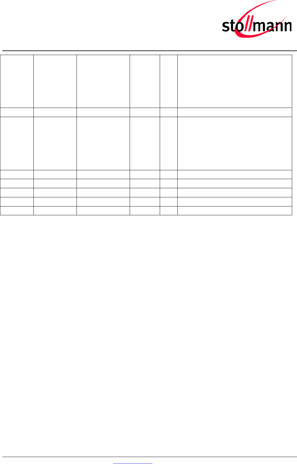
4.2.2.1 SPP Pin Configuration
Type: PU – Pull-up; PD – pull-down; PWR – Power; I – Input; O – Output; I/O – bidir.; OD – open drain: PP – push/pull; RF: RadioFreq
Pin Name Signal SPP-Function Type Act Description
E-6 VSUP1 Power PWR +3,3V nom.
F-6 VSUP2 Power PWR +3,3V nom
C-1 VSUP3 Power PWR +3,3V nom
A-7,E-7,F-
7,
B-[5,6,7,8],
C-
[5,6,7,8],
D-8, E-8,
F-8
GND Power PWR Ground
A-8 ANT Antenna RF n.c. (/AI) or RF (/AP)
B-1 EXT-RES# Reset I/O-PU L User Reset
A-6 SLCK SLCK I-PD 32,768kHz Slow Clock (optional)
F-4 UART-TXD TXD O-PP IUR Data OUT
D-2 UART-RXD RXD I-PD IUR Data IN
D-7 UART-RTS# /RTS O-PP
(1)
L Flow Control/IUC; refer to [3]
F-3 UART-CTS# /CTS I-PD L Flow Control/IUC; refer to [3]
B-4 IUR-OUT# /IUR-OUT O-PP
(1)
L UICP Control; refer to [3]
D-5 IUR-IN# /IUR-IN I-PD L UICP Control; refer to [3]
D-3 GPIO[0] GPIO0 I GPIO
(3)
B-2 GPIO[1] GPIO1 I GPIO
(3)
D-1 GPIO[2] IOC I/O User IO
E-4 GPIO[3] IOB
User IO
D-4 GPIO[4] HANGUP I-PD optional; refer to [5]
F-2 GPIO[5] IOD I/O User IO
C-4 GPIO[6] reserved O-PP Debug UART TXD
C-3 GPIO[7] GPIO7 I-PD GPIO
(3)
E-2 GPIO[8] IOA I/O User IO
A-3 BT-ACT WLAN coexistence O
A-1 BT-STAT WLAN coexistence O
A-4 WLAN-DNY WLAN coexistence I-PD
A-2 BT-PER WLAN coexistence O
F-1 TESTMODE# reserved I-PU L leave open
BlueMod+SR/AI
BlueMod+SR/AP
Hardware Reference
Release r04d01 www.stollmann.de Page 25 of 65
E-1 BOOT0
r
I-PD (2) system memory bootloader
E-3 DNU
(4)
reserved leave open (serial wire)
D-6 DNU (4)
r
leave open (serial wire)
C-2 DNU
(4)
reserved leave open
B-3 DNU
(4)
reserved leave open
A-5 DNU
(4)
reserved
leave open
F-5 DNU
(4)
reserved leave open
E-5 DNU
(4)
reserved leave open
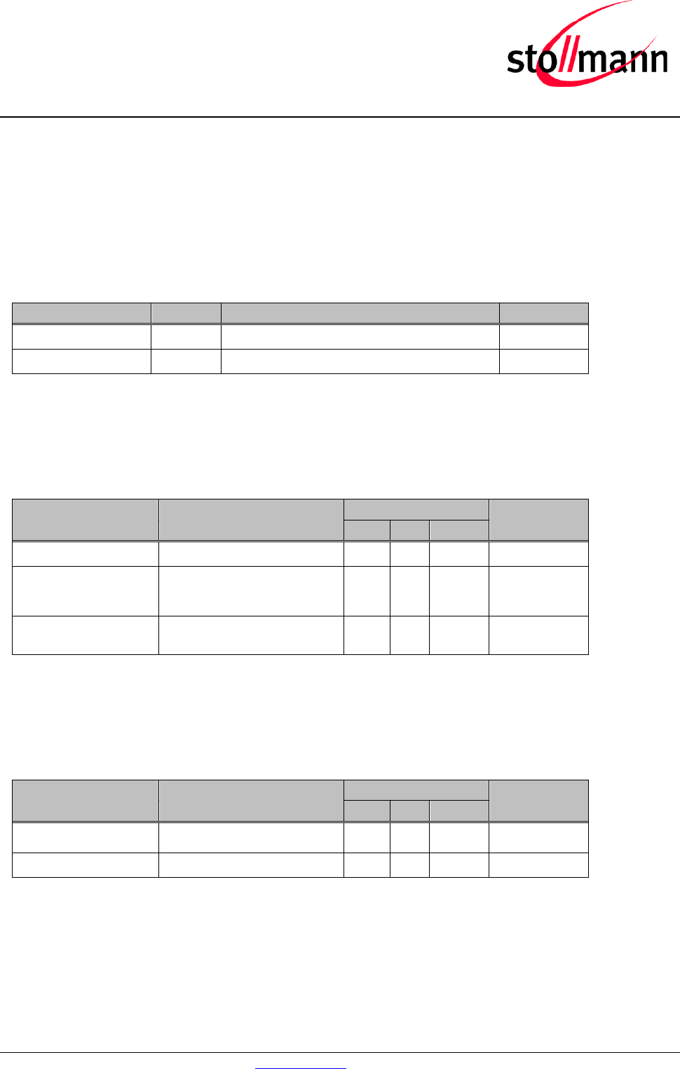
Table 5: Application Specific Pin Assignments, SPP
Notes:
(1) a discrete pull-up resistor is used
(2) a discrete pull-down resistor is used
(3) function depends on firmware
(4) DNU: Do Not Use, Do Not Connect
4.3 Handling of Unused Signals
Depending on the application, not all signals of BlueMod+SR may be needed. The following list
gives some hints how to handle unused signals.
• EXT-RES# If no external Reset is needed: Leave open (*)
• BOOT0 (*) [leave open]
• SLCK If no external slow clock is provided: Leave open or tie to
GND
• UART-RTS#, UART-CTS# If neither flow control nor UICP is used: Leave open
• IUR-OUT#, IUR-IN# If UICP is not used: leave open
• BT-ACT, BT-STAT, If there is no WLAN device on the same PCB: Leave open
BT-PER, WLAN-DNY
• TESTMODE# Leave open
• unused GPIOs Leave open
• SWDIO, SWCLK Leave open. Only needed for debug purposes.
(*) for being able to update the firmware, it is strongly recommended to provide for a means to set
BOOT0 temporarily to logic high level, and to reset the module; see chapter 3.13.
BlueMod+SR/AI
BlueMod+SR/AP
Hardware Reference
Release r04d01 www.stollmann.de Page 27 of 65
5 Electrical Characteristics
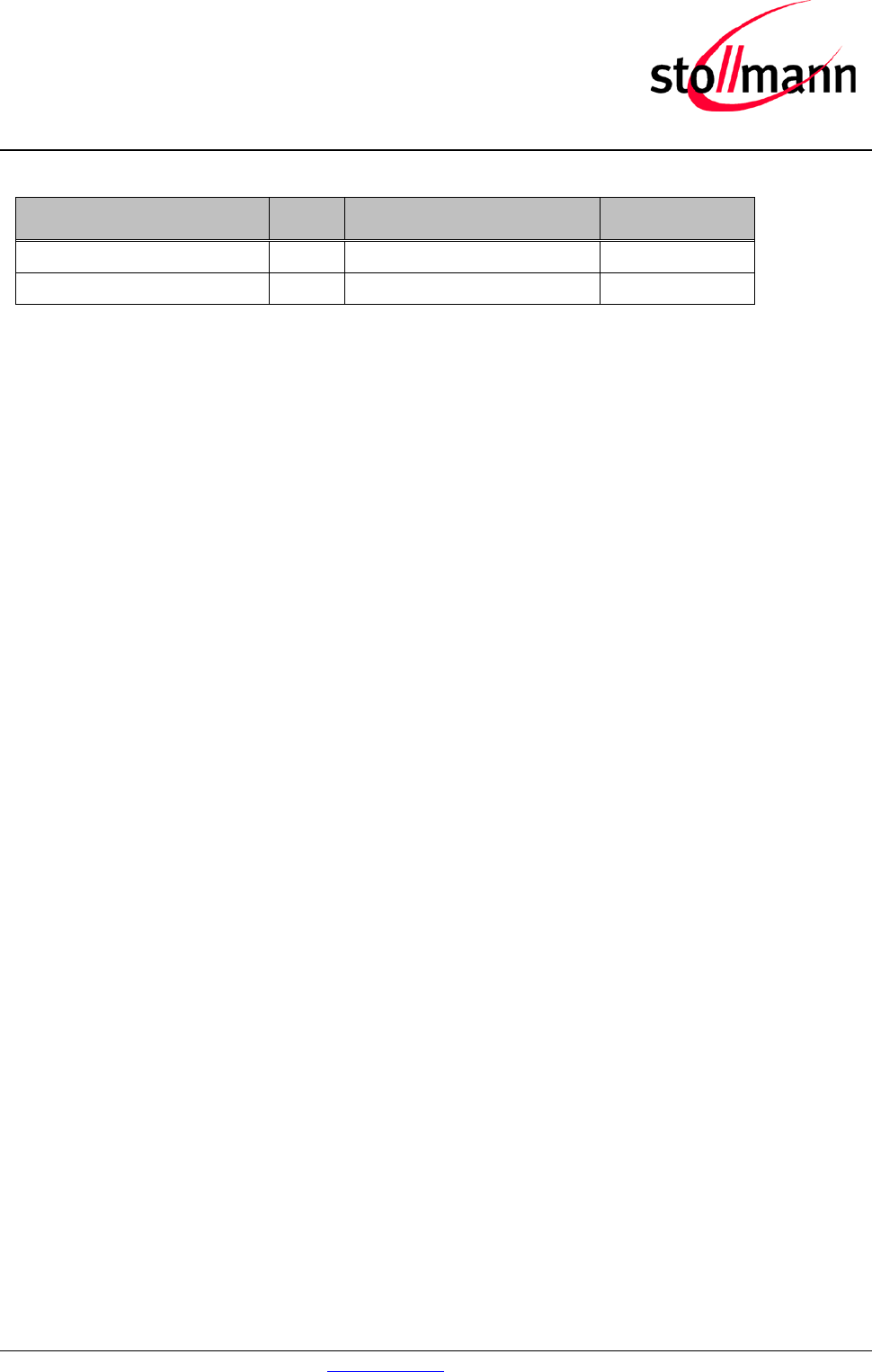
5.1 Absolute Maximum Ratings
Stresses beyond those listed under “Absolute Maximum Ratings” may cause permanent damage
to the device. These are stress ratings only, and functional operation of the device at these or any
other conditions beyond those indicated under “Electrical Requirements” is not implied. Exposure
to absolute-maximum-rated conditions for extended periods may affect device reliability.
Item Symbol Absolute Maximum Ratings Unit
Supply voltage VSUP -0,3 to +3,6 V
Voltage on any pin VPin -0,3 to VSUP +0,4 V
Table 6: Absolute Maximum Ratings
5.2 Electrical Requirements
VSUP = 3,3V, Tamb = 25°C if nothing else stated
Item Condition Limit Unit
Min Typ Max
Frequency Range 2400 2483.5 MHz
Load impedance Measured with network
analyzer in the frequency
range at antenna pin 50 Ohm
Output return loss Receive Mode to 50Ω load
Transmit Mode to 50Ω load
-10
-10 dBm
Table 7: Electrical Requirements
5.3 Operating Conditions
Tamb = 25°C
Item Condition Limit Unit
Min Typ Max
Supply voltage VSUP 2,5 3,3 3,6 VDC
Ripple on VSUP Ripple frequency ≤10MHz 10 mVrms
Table 8: DC Operating Conditions
BlueMod+SR/AI
BlueMod+SR/AP
Hardware Reference
Release r04d01 www.stollmann.de Page 28 of 65
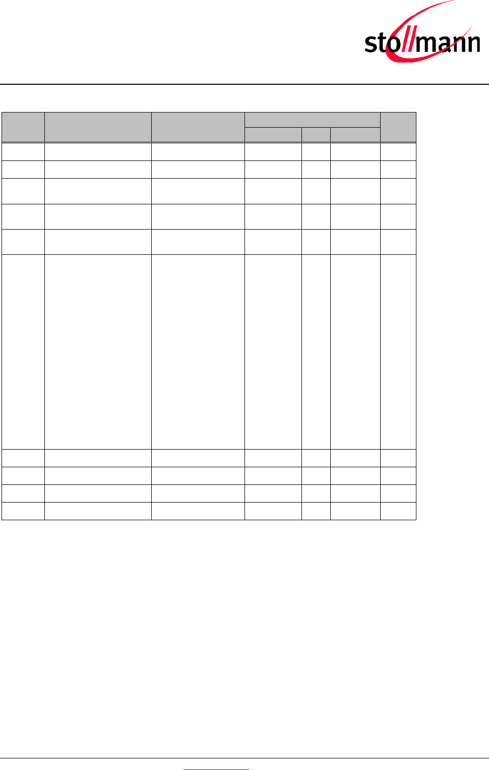
5.4 Environmental Requirements
Item Symbol Absolute Maximum Ratings Unit
Storage temperature range Tstg -40 to +85 °C
Operating temperature range Top -30 to +85 °C
Table 9: Environmental Requirements
5.5 Digital I/O Including EXT-RES#
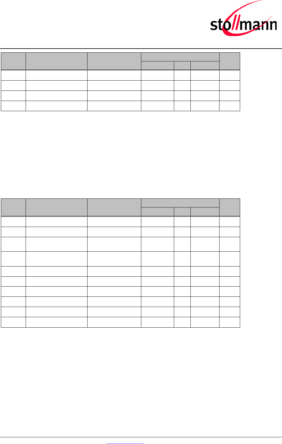
STM32 MCU and CSR8811 do have different electrical I/O characteristics.
All Module I/O pins are connected directly to these chips without signal conditioning except for
some pull-up/pull-down resistors (as indicated). Therefore the electrical characteristics are split in
different tables.
STM-Related Signals:
• EXT-RES# (additional filter-C 100n to GND)
• UART-TXD, UART-RXD, UART-CTS#
• UART-RTS# (pull-up resistor 470kΩ)
• IUR-IN#
• IUR-OUT# (pull-up resistor 470kΩ)
• GPIO[0..8], TESTMODE#
• BOOT0 (pull-down resistor 100kΩ)
BlueMod+SR/AI
BlueMod+SR/AP
Hardware Reference
Release r04d01 www.stollmann.de Page 29 of 65
Tamb = 25°C
Symbol Item Condition Limit Unit
Min Typ Max
VIL Low-Level Input Voltage VSUP = 2,5 to 3,6V -0,3 - 0,9 V
VIH High-Level Input Voltage VSUP = 2,5 to 3,6V 2,0 - VSUP+0,3 V
VOL Low-Level Output
Voltage IOL = 4mA - - 0,4 V
VOH High-Level Output
Voltage IOH = -4mA VSUP-0,4 - - V
IOL Low -Level Output
Current VOL = 0,4V - - 8 mA
IOH High-Level Output
Current
2,
7
V
<
V
S
U
P
<
3
,
6
V
VOH = 2.3V
- - -8 mA
RPU weak pull-up resistor VIN = VSS 30 40 50 kΩ
RPD weak pull-down resistor VIN = VDD 30 40 50 kΩ
Ilc I/O pad leakage current -3 0 +3
µ
A
Cl Input Capacitance 5 pF
Table 10: DC Characteristics, Digital IO (STM32-related)
External Slow Clock SLCK:
Tamb = 25°C
BlueMod+SR/AI
BlueMod+SR/AP
Hardware Reference
Release r04d01 www.stollmann.de Page 30 of 65
Symbol Item Condition Limit Unit
Min Typ Max
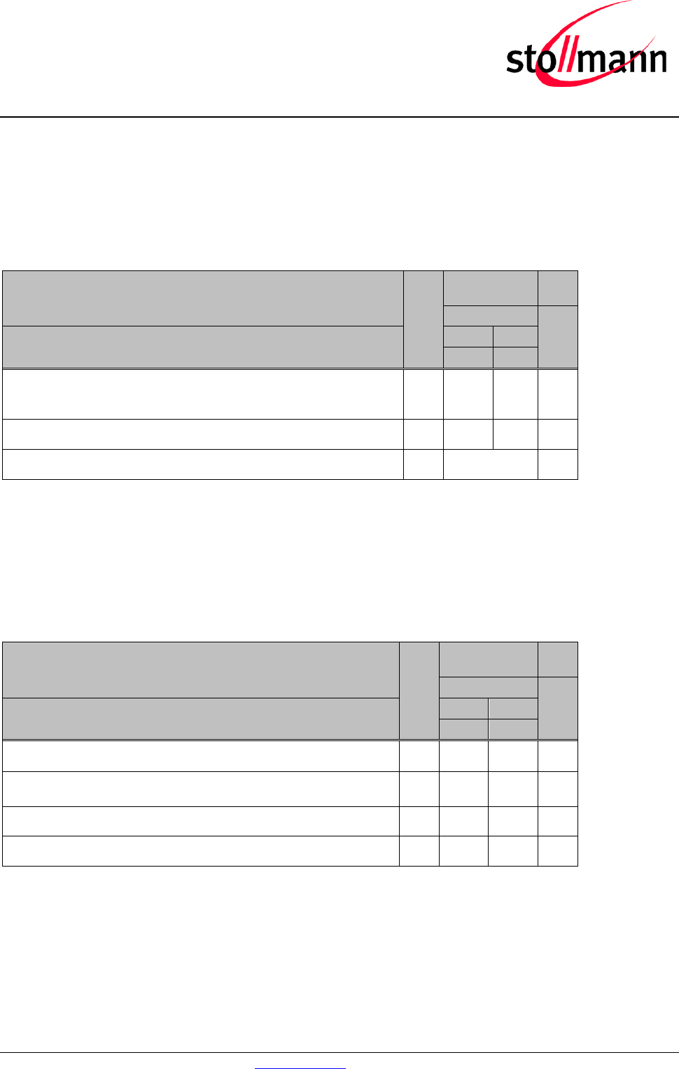
VLSEL Low-Level Input Voltage VSUP = 2,5 to 3,6V 0,0 - 0,3 V
VLSEH High-Level Input Voltage VSUP = 2,5 to 3,6V 0,7xVSUP - VSUP V
Ilc I/O pad leakage current VSS ≤ VIN ≤ VSUP -1 - +1 µA
Cl Input Capacitance 5 pF
Table 11: DC Characteristics, SLCK (STM32 Backup Domain)
Note: Signal at SLCK is also fed to CSR8811 and has to comply to Table 12, too.
CSR8811 Related Signals:
• BT-ACT, BT-STAT, WLAN-DNY, BT-PER
• SLCK (caution: also connected to STM-32!)
Tamb = 25°C
Symbol Item Condition Limit Unit
Min Typ Max
VIL Low-Level Input Voltage VSUP = 3,3V - 0,4 - 0,4 V
VIH High-Level Input Voltage 0,7xVSUP - VSUP+0,4 V
VOL Low-Level Output
Voltage IOL = 4mA - - 0,4 V
VOH High-Level Output
Voltage IOH = -4mA 0,75xVSUP - - V
Isp-u Input-current Strong pull-up -150 -40 -10 µA
Isp-d Input-current Strong pull-down +10 +40 -+150 µA
Iwp-u Input-current Weak pull-up -5,0 -1,0 -0,33 µA
Iwp-d Input-current Weak pull-down +0,33 -1,0 +5,0 µA
Ilc I/O pad leakage current n.a. µA
Cl Input Capacitance 1,0 - 5,0 pF
Table 12: DC Characteristics, Digital IO (CSR8811 Related)
Note: SLCK is connected to both STM32 and CSR8811 so has to fit to STM32 and CSR8811
requirements at the same time.
BlueMod+SR/AI
BlueMod+SR/AP
Hardware Reference
Release r04d01 www.stollmann.de Page 31 of 65
5.6 Power Consumption and Power Down Modes
5.6.1 SPP Configuration
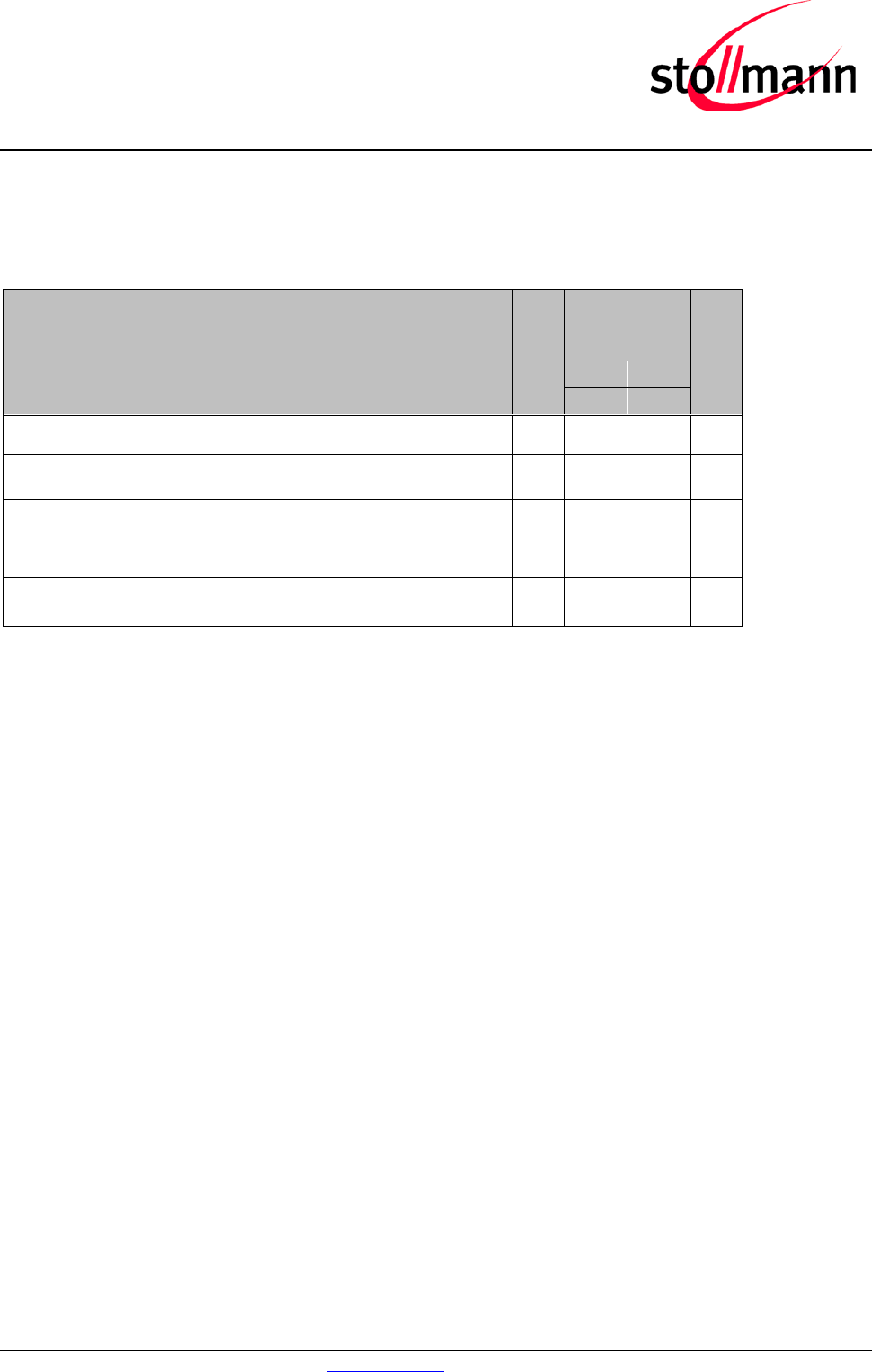
The following values are typical power consumption values in the different states.
VSUP = 3,3V, Tamb = 25°C, all GPIOs and UART lines open, SLCK: 32,768 kHz
Condition Note Current
Consumption Unit
Slow clock
Extern Intern
IAvg IAvg
standby, no page scan, no inquiry scan
3,7 mA
standby, no page scan, no inquiry scan, UICP active Interface down (1) 0,21 0,36 mA
device in reset (2) 2,7 mA
Table 13: Supply Current SPP Standby Modes no Radio Activity
Notes:
(1) IUR-IN# and UART-CTS# signals connected to VSup
(2) Valid for HW V3, higher in Hw Version < 3
VSUP = 3,3V, Tamb = 25°C, Tx Power = 7 dBm, all GPIOs and UART lines open
Condition Note Current
Consumption Unit
Slow clock
Extern
Intern
IAvg IAvg
standby, page scan & inquiry scan interval 1.28s 4,0 4,2 mA
standby, page scan & inquiry scan interval 1.28s,UICP active serial
Interface down (1) 0,8 1,0 mA
Bluetooth connected, no data traffic – close range (Slave) (2) 14,4 14,4 mA
Bluetooth connected, data traffic 115 kbit/s – close range (Slave) (2) 21,1 21,1 mA
Table 14: Supply Current, SPP Bluetooth Classic
Notes:
(1) IUR-IN# and UART-CTS# signals connected to VSup
(2) about 2 meters through the air
BlueMod+SR/AI
BlueMod+SR/AP
Hardware Reference
Release r04d01 www.stollmann.de Page 32 of 65
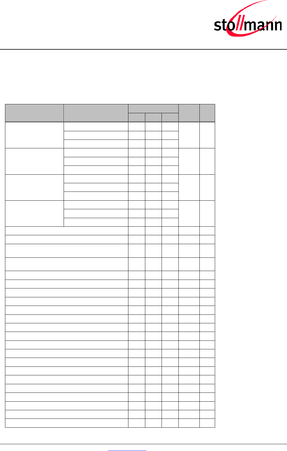
The following table shows the average power consumption of BlueMod+SR in LE-mode operating
in the peripheral device role.
VSUP = 3,3V, Tamb = 25°C, Tx power = +7 dBm, all GPIOs and UART lines open
Condition Note Current
Consumption Unit
Slow clock
Extern
Intern
I
Avg
I
Avg
Idle, Advertising on 3 channels, advertising interval: 1,28s 3,5 3,7 mA
Idle, Advertising on 3 channels, advertising interval: 1,28s, UICP
active serial Interface down 0,31 0,46 mA
Connected, connection interval: 40ms, no data traffic (2,3) 4,8 5,0 mA
Connected, connection interval: 37,5ms, no data traffic (2,4)
5,3 5,4 mA
Connected, connection interval: 37,5ms
data traffic
(2,4) Tbd Tbd mA
Table 15: Supply Current BLE Peripheral Device Role
Notes:
(2) connection parameters are setup by the central device when connection is established
(3) no data to be transmitted, central device sends an empty packet (80 bit) then peripheral device answers (empty
packet: 80 bit)
(4) these are a typical connection parameters used by an iPhone, iPad or iPad mini device in the central device role
BlueMod+SR/AI
BlueMod+SR/AP
Hardware Reference
Release r04d01 www.stollmann.de Page 33 of 65
5.7 RF Performance
5.7.1 GFSK, PI/4 DQPSK, 8DPSK Receiver
VSUP = 2,5V to 3,6V, Tamb = 20°C
Measured conducted according to BT specification v1.2/2.0/2.0 + EDR/2.1/2.1 + EDR/3.0/3.0 + HS/4.0
Receiver
Frequency [GHz] Limit BT
Unit
Min Typ Max Spec
Sensitivity at 0.1% BER
DH1
2.402 -84 -80
≤-70 dBm
2.441 -88 -84
2.480 -88 -84
Sensitivity at 0.1% BER
DH5
2.402 -84 -80
≤-70 dBm
2.441 -88 -84
2.480 -88 -84
Sensitivity at 0.1% BER
EDR2, PI/4 DQPSK
2.402 -87 -70
≤-70 dBm
2.441 -91 -70
2.480 -91 -70
Sensitivity at 0.1% BER
EDR3, 8DPSK
2.402 -78 -70
≤-70 dBm
2.441 -82 -70
2.480 -82 -70
Maximum received signal at 0.1% BER with DH1 -20 0 ≥-20 dBm
Maximum received signal at 0.1% BER with DH5 -20 0 ≥-20 dBm
Maximum received signal at 0.1% BER with EDR2, PI/4
DQPSK -20 0 ≥-20 dBm
Maximum received signal at 0.1% BER with EDR3,
8DPSK -20 0 ≥-20 dBm
C/I co-channel GFSK 8 11 ≤ 11 dB
Adjacent channel selectivity C/I f = f0 + 1MHz GFSK -2 0 ≤ 0 dB
Adjacent channel selectivity C/I f = f0 - 1MHz GFSK -1 0 ≤ 0 dB
Adjacent channel selectivity C/I f ≥ f0 + 2MHz GFSK -39 -30 ≤ -30 dB
Adjacent channel selectivity C/I f ≤ f0 - 2MHz GFSK -30 -30 ≤ -20 dB
Adjacent channel selectivity C/I f ≥ f0 + 3MHz GFSK -45 -40 ≤ -40 dB
Adjacent channel selectivity C/I f ≤ f0 - 5MHz GFSK -46 -40 ≤ -40 dB
Adjacent channel selectivity C/I f = fimage GFSK -25 -9 ≤ -9 dB
C/I co-channel PI/4 DQPSK 12 13 ≤ 13 dB
Adj. channel selectivity C/I f = f0 + 1MHz π/4 DQPSK -7 0 ≤ 0 dB
Adj. channel selectivity C/I f = f0 - 1MHz π/4 DQPSK -4 0 ≤ 0 dB
Adj. channel selectivity C/I f ≥ f0 + 2MHz π/4 DQPSK -40 -30 ≤ -30 dB
Adj. channel selectivity C/I f ≤ f0 - 2MHz π/4 DQPSK -36 -20 ≤ -20 dB
Adj. channel selectivity C/I f ≥ f0 + 3MHz π/4 DQPSK -48 -40 ≤ -40 dB
Adj. channel selectivity C/I f ≤ f0 - 5MHz π/4 DQPSK -50 -40 ≤ -40 dB
Adj. channel selectivity C/I f = fimage π/4 DQPSK -22 -7 ≤ -7 dB
C/I co-channel 8DPSK 18 21 ≤ 21 dB
BlueMod+SR/AI
BlueMod+SR/AP
Hardware Reference
Release r04d01 www.stollmann.de Page 34 of 65
Receiver Frequency [GHz] Limit BT Unit
Min Typ Max Spec
Adj. channel selectivity C/I f = f0 + 1MHz 8DPSK -4 5 ≤ 5 dB
Adj. channel selectivity C/I f = f0 - 1MHz 8DPSK -1 5 ≤ 5 dB
Adj. channel selectivity C/I f ≥ f0 + 2MHz 8DPSK -36 -25 ≤ -25 dB
Adj. channel selectivity C/I f ≤ f0 - 2MHz 8DPSK -31 -13 ≤ -13 dB
Adj. channel selectivity C/I f ≥ f0 + 3MHz 8DPSK -42 -33 ≤ -33 dB
Adj. channel selectivity C/I f ≤ f0 - 5MHz 8DPSK -43 -33 ≤ -33 dB
Adj. channel selectivity C/I f = fimage 8DPSK -14 0 ≤ -0 dB
BlueMod+SR/AI
BlueMod+SR/AP
Hardware Reference
Release r04d01 www.stollmann.de Page 35 of 65
VSUP = 2,5V to 3,6V, Tamb = -30°C
Measured conducted according to BT specification v1.2/2.0/2.0 + EDR/2.1/2.1 + EDR/3.0/3.0 + HS/4.0
Receiver
Frequency [GHz] Limit BT Unit
Min Typ Max Spec
Sensitivity at 0.1% BER
DH1
2.402 -84 -80
≤-70 dBm
2.441 -88 -84
2.480 -88 -84
Sensitivity at 0.1% BER
DH5
2.402 -84 -80
≤-70 dBm
2.441 -88 -84
2.480 -88 -84
Sensitivity at 0.1% BER
EDR2, PI/4 DQPSK
2.402 -88 -70
≤-70 dBm
2.441 -91 -70
2.480 -91 -70
Sensitivity at 0.1% BER
EDR3, 8DPSK
2.402 -78 -70
≤-70 dBm
2.441 -82 -70
2.480 -82 -70
Maximum received signal at 0.1% BER DH1 -20 0 ≥-20 dBm
Maximum received signal at 0.1% BER PI/4 DQPSK -20 0 ≥-20 dBm
Maximum received signal at 0.1% BER 8DPSK -20 0 ≥-20 dBm
VSUP = 2,5V to 3,6V, Tamb = +85°C
Measured conducted according to BT specification v1.2/2.0/2.0 + EDR/2.1/2.1 + EDR/3.0/3.0 + HS/4.0
Receiver Frequency [GHz] Limit BT Unit
Spec
Sensitivity at 0.1% BER
DH1
2.402 -84 -80
≤-70 dBm
2.441 -88 -84
2.480 -88 -84
Sensitivity at 0.1% BER
DH5
2.402 -84 -80
≤-70 dBm
2.441 -88 -84
2.480 -88 -84
Sensitivity at 0.1% BER
EDR2, PI/4 DQPSK
2.402 -87 -70
≤-70 dBm
2.441 -90 -70
2.480 -90 -70
Sensitivity at 0.1% BER
EDR3, 8DPSK
2.402 -78 -70
≤-70 dBm
2.441 -80 -70
2.480 -80 -70
Maximum received signal at 0.1% BER DH1 -20 0 ≥-20 dBm
Maximum received signal at 0.1% BER PI/4 DQPSK -20 0 ≥-20 dBm
Maximum received signal at 0.1% BER 8DPSK -20 0 ≥-20 dBm
Table 16: RF Performance GFSK, PI/4 DQPSK, 8DPSK Receiver
Notes:
(b) For calculating true performance add product specific antenna gain
BlueMod+SR/AI
BlueMod+SR/AP
Hardware Reference
Release r04d01 www.stollmann.de Page 36 of 65
5.7.2 GFSK, PI/4 DQPSK, 8DPSK Transmitter
VSUP = 2,5V to 3,6V, Tamb = +20°C
Measured conducted according to BT specification v1.2/2.0/2.0 + EDR/2.1/2.1 + EDR/3.0/3.0 + HS/4.0
Trans
mitt
er Frequency [GHz] Limit BT
Unit
RF transmit power
50 Ω load, at antenna
Class 1 device GFSK b)
2.402 2,7 5,5
0 to 20 dBm
2.441 4,7 7,5
2.480 5,7 8,5
RF transmit power
50 Ω load, at antenna
Class 1 device EDR2, π/4
DQPSK b)
2.402 GFSK 2,0
∆TX =
-4 to 1 dBm
2.402 π/4 DQPSK 0,9
2.441 GFSK 4,7
2.441 π/4 DQPSK 3,7
2.480 GFSK 5,6
2.480 π/4 DQPSK 4,6
RF transmit power
50 Ω load, at antenna
Class 1 device EDR3, 8DPSK
b)
2.402 GFSK 2,1
∆TX =
-4 to 1 dBm
2.402 8DPSK 1,0
2.441 8GFSK 4,8
2.441 8DPSK 3,7
2.480 GFSK 5,6
2.480 8DPSK 4,6
RF power control range 16 30 ≥16 dB
RF power range control resolution 2 4 8 2 to 8 dB
20 dB bandwidth for modulated carrier 925 1000 ≤1000 kHz
ICFT -75 ±25 +75 ≤ ±75 kHz
Carrier frequency drift (packet DH1) 7 25 ≤ 25 kHz
Drift Rate 5 20 ≤ 20 kHz/
50µs
∆f1avg “Maximum Modulation” 140 164 175 ≥140 to
≤175 kHz
∆f2max “Minimum Modulation” 115 140 >115 kHz
∆f2avg /∆f1avg 0,8 0,91 ≥ 0,8
BlueMod+SR/AI
BlueMod+SR/AP
Hardware Reference
Release r04d01 www.stollmann.de Page 37 of 65
VSUP = 2,5V to 3,6V, Tamb = -30°C
Measured conducted according to BT specification v1.2/2.0/2.0 + EDR/2.1/2.1 + EDR/3.0/3.0 + HS/4.0
Trans
mitt
er Frequency [GHz] Limit BT
Unit
RF transmit power
50 Ω load, at antenna
Class 1 device GFSK b)
2.402 2,7 3,5
0 to 20 dBm
2.441 4,7 6,5
2.480 5,7 7,5
RF transmit power
50 Ω load, at antenna
Class 1 device EDR2, π/4
DQPSK b)
2.402 GFSK -0,5
∆TX =
-4 to 1 dBm
2.402 π/4 DQPSK -1,9
2.441 GFSK 2,5
2.441 π/4 DQPSK 1,2
2.480 GFSK 4,0
2.480 π/4 DQPSK 2,8
RF transmit power
50 Ω load, at antenna
Class 1 device EDR3, 8DPSK
b)
2.402 GFSK -0,5
∆TX =
-4 to 1 dBm
2.402 8DPSK -1,7
2.441 GFSK 2,5
2.441 8DPSK 1,2
2.480 GFSK 4,0
2.480 8DPSK 2,8
20 dB bandwidth for modulated carrier 925 1000 ≤1000 kHz
Initial carrier frequency tolerance -75 10 +75 ≤ ±75 kHz
Carrier frequency drift (packet DH1) 6 25 ≤ 25 kHz
Drift Rate 5 20 20 kHz/
50µs
∆f1avg “Maximum Modulation” 140 164 175 ≥140 to
≤175 kHz
∆f2max “Minimum Modulation” 115 142 ≥ 115 kHz
∆f2avg /∆f1avg 0,8 0,92 ≥ 0,8
BlueMod+SR/AI
BlueMod+SR/AP
Hardware Reference
Release r04d01 www.stollmann.de Page 38 of 65
VSUP = 2,5V to 3,6V, Tamb = +85°C
Measured conducted according to BT specification v1.2/2.0/2.0 + EDR/2.1/2.1 + EDR/3.0/3.0 + HS/4.0
Transmitter
Frequency [GHz] Limit BT Unit
RF transmit power
50 Ω load, at antenna
Class 1 device GFSK b)
2.402 1,8 4,0
0 to 20 dBm
2.441 3,8 6,0
2.480 4,8 7,0
RF transmit power
50 Ω load, at antenna
Class 1 device EDR2, π/4
DQPSK b)
2.402 GFSK 0,3
∆TX =
-4 to 1 dBm
2.402 π/4 DQPSK -0,8
2.441 GFSK 2,8
2.441 π/4 DQPSK 1,7
2.480 GFSK 4,0
2.480 π/4 DQPSK 2,9
RF transmit power
50 Ω load, at antenna
Class 1 device EDR3, 8DPSK
b)
2.402 GFSK 0,3
∆TX =
-4 to 1 dBm
2.402 8DPSK -0,8
2.441 GFSK 2,8
2.441 8DPSK 1,7
2.480 GFSK 4,0
2.480 8DPSK 2,9
20 dB bandwidth for modulated carrier 925 1000 ≤1000
Initial carrier frequency tolerance -75 10 +75 ≤ ±75
Carrier frequency drift (packet DH1) 7 25 ≤ 25
Drift Rate 5 20 20
∆f1avg “Maximum Modulation” 140 164 175 ≥140 to
≤175
∆f2max “Minimum Modulation” 115 140 ≥ 115 kHz
∆f2avg /∆f1avg 0,8 0,91 ≥ 0,8
Table 17: RF Performance GFSK, PI/4 DQPSK, 8DPSK Transmitter
Notes:
(b) For calculating true performance add product specific antenna gain
BlueMod+SR/AI
BlueMod+SR/AP
Hardware Reference
Release r04d01 www.stollmann.de Page 39 of 65
5.7.3 BLE Receiver
VSUP = 2,5V to 3,6V, Tamb = +20°C
Measured conducted according to BT specification RF-PHY.TS/4.0.1
Receiver Frequ
/GHz Min Typ Max BT
Spec Unit
Sensitivity at 30,8% PER
2,402
-87
-83
≤ -70 dBm
2,440
-90
-86
2,480
-90 -86
Reported PER during PER
report integrity test 2,426 50 50 65,4
50
< PER
< 65,4
%
Maximum received signal at 30,8% PER
-10 0 ≥ -10 dBm
Continuous power required to
block Bluetooth reception at -
67dBm with 0,1%PER
0,030 - 2,000
-30
> 0
-30
dBm
2,000 - 2,400
-35
0
-35
2,500 -3,000
-35
0
-35
3,000 . 12,75
-30
>0
-30
C/I co-channel
8
21
≤21
dB
Adjacent channel
Selectivity C/I
F = F
0
+ 1 MHz
1 15 ≤15 dB
F = F
0
- 1 MHz
-9 15 ≤15 dB
F = F
0
+ 2 MHz
-27
-17
≤-17
dB
F = F
0
- 2 MHz
-19
-15
≤-15
dB
F = F
0
+ 3 MHz
-43
-27
≤-27
dB
F = F
0
- 5 MHz
-49
-27
≤-27
dB
F = F
image
-24
-9
≤-9
dB
Maximum level of intermodulation interferers
-50 -18 ≥-50 dBm
VSUP = 2,5V to 3,6V, Tamb = -30°C
Measured conducted according to BT specification RF-PHY.TS/4.0.1
Receiver Frequ
/GHz Min Typ Max BT
Spec Unit
Sensitivity at 30,8% PER
2,402
-87
-83
≤ . 70 dBm
2,440
-90
-87
2,480
-90 -87
Reported PER during PER
report integrity test 2,426 50 50 65,4
50
< PER
< 65,4
%
Maximum received signal at 30,8% PER
-10 0 ≥ -10 dBm
VSUP = 2,5V to 3,6V, Tamb = +85°C
Measured conducted according to BT specification RF-PHY.TS/4.0.1
Receiver Frequ
/GHz Min Typ Max BT
Spec Unit
Sensitivity at 30,8% PER
2,402
-87
-83
≤ . 70 dBm
2,440
-89 -85
2,480
-89 -85
Reported PER during PER
report integrity test 2,426 50 50 65,4
50
< PER
< 65,4
%
Maximum received signal at 30,8% PER
-10 0 ≥ -10 dBm
Table 18: RF Performance BLE Receiver
BlueMod+SR/AI
BlueMod+SR/AP
Hardware Reference
Release r04d01 www.stollmann.de Page 40 of 65
5.7.4 BLE Transmitter
VSUP = 2,5V to 3,6V, Tamb = +20°C
Measured conducted according to BT specification RF-PHY.TS/4.0.1
Transmitter Frequ
/GHz Min Typ Max BT
Spec Unit
RF Transmit Power
2,402
2,0
5,5
10
-20 to
+10 dBm
2,440
4,0
7,5
10
2,480
5,0 8,5 10
ACP
F = F
0
± 2MHz
-28
-20
≤ -30
dBm
F = F
0
± 3MHz
-38
-30
≤ -30
F = F
0
± > 3MHz
<-60
-30
≤ -30
∆f
1avg
maximum modulation
225 268 275
225
< f1avg
< 275
kHz
∆f
2max
minimum modulation
185
214
≥ 185
kHz
∆f
2avg
/ ∆f
1avg
0,8
0,83
≥ 0,8
Frequency Offset
-95
±25
+95
± 150
kHz
Carrier drift rate
4 20 ≤ 20
kHz/
50µs
Carrier drift
5 50 ≤ 50 kHz
VSUP = 2,5V to 3,6V, Tamb = -30°C
Measured conducted according to BT specification RF-PHY.TS/4.0.1
Transmitter Frequ
/GHz Min Typ Max BT
Spec Unit
RF transmit Power
2,402
0,5
4,0
10
-20 to
+10 dBm
2,440
2,5
6,5
10
2,480
3,5
7,5
10
ACP
F = F
0
± 2MHz
-28 -20 ≤ -30
dBm
F = F
0
± 3MHz
-35 -30 ≤ -30
F = F
0
± > 3MHz
<-60
-30
≤ -30
∆f
1avg
maximum modulation
225 266 275
225
< f1avg
< 275
kHz
∆f
2max
minimum modulation
185
225
≥ 185
kHz
∆f
2avg
/ ∆f
1avg
0,8
0,85
≥ 0,8
Frequency Offset
-95
±25
+95
± 150
kHz
Carrier drift rate
4 20 ≤ 20
kHz/
50µs
Carrier drift
5
50
≤ 50
kHz
BlueMod+SR/AI
BlueMod+SR/AP
Hardware Reference
Release r04d01 www.stollmann.de Page 41 of 65
VSUP = 2,5V to 3,6V, Tamb = +85°C
Measured conducted according to BT specification RF-PHY.TS/4.0.1
Transmitter Frequ
/GHz
Min Typ Max BT
Spec
Unit
RF transmit Power
2,402
1,0
4,0
10
-20 to
+10 dBm
2,440
3,0
6,0
10
2,480
4,0
7,0
10
ACP
F = F
0
± 2MHz
-30
-20
≤ -30
dBm
F = F
0
± 3MHz
-42 -40 ≤ -30
F = F
0
± > 3MHz
<-60 -30 ≤ -30
∆f
1avg
maximum modulation
225 267 275
225
< f1avg
< 275
kHz
∆f
2max
minimum modulation
185
214
≥ 185
kHz
∆f
2avg
/ ∆f
1avg
0,8
0,83
≥ 0,8
Frequency Offset
-95
±25
+95
± 150
kHz
Carrier drift rate
5 20 ≤ 20
kHz/
50µs
Carrier drift
5
50
≤ 50
kHz
Table 19: RF Performance BLE Transmitter
BlueMod+SR/AI
BlueMod+SR/AP
Hardware Reference
Release r04d01 www.stollmann.de Page 42 of 65
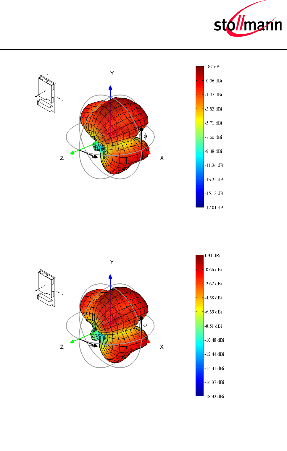
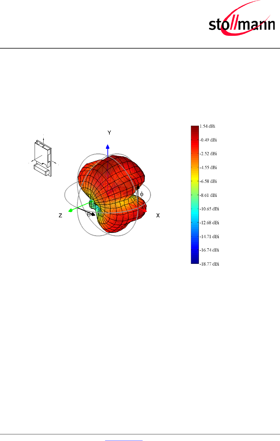
5.7.5 Antenna-Gain and Radiation Pattern
If BlueMod+SR/AI is integrated into an end product while the recommendations depicted in 6.4
Placement Recommendation are maintained, the following typical antenna radiation patterns can
be expected.
Radiation Pattern will depend on the end products PCB size, masses in the antenna environment,
housing material and geometrics.
Figure 11: Typical Antenna Radiation Pattern at 2402MHz
Y
X
Z

BlueMod+SR/AI
BlueMod+SR/AP
Hardware Reference
Release r04d01 www.stollmann.de Page 44 of 65
5.8 Power-Up Time
The time until the BlueMod+SR is able to accept link requests or serial data depends on the
firmware version. In the SPP firmware version 1.103 the module is command ready after at least
1,1 s. Bluetooth links are accepted tbd s after reset.
Note: For further information refer to the document BlueMod+SR_Startup_Timing_r01 [6]
BlueMod+SR/AI
BlueMod+SR/AP
Hardware Reference
Release r04d01 www.stollmann.de Page 45 of 65
6 Mechanical Characteristics
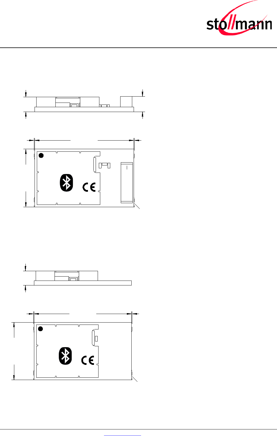
6.1 Dimensions
17,0
+0,2
-0,0
FCC ID RFRMSR
stollmann
BlueMod+SR
2,5
10,0
+0,2
-0,0
0,1
+0,1
-0,1
0,1
+0,1
-0,1
Verbleibende Stege nach Nutzentrennung/
remaining break tabs after separation
2,6
Figure 14: BlueMod+SR/AI dimensions
17,0
+0,2
-0,0
FCC ID RFRMSR
stollmann
BlueMod+SR
2,5
10,0
+0,2
-0,0
0,1
+0,1
-0,1
0,1
+0,1
-0,1
Verbleibende Stege nach Nutzentrennung/
remaining break tabs after separation
Figure 15: BlueMod+SR/AP Dimensions
BlueMod+SR/AI
BlueMod+SR/AP
Hardware Reference
Release r04d01 www.stollmann.de Page 47 of 65
6.3 Re-flow Temperature-Time Profile
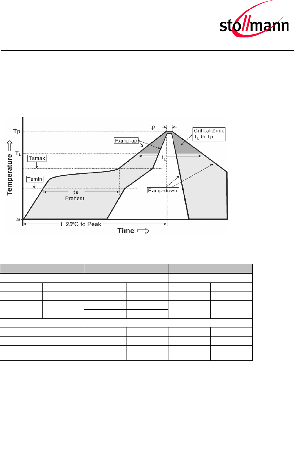
The data here is given only for guidance on solder and has to be adapted to your process and
other re-flow parameters for example the used solder paste. The paste manufacturer provides a re-
flow profile recommendation for his product.
Figure 17: Soldering Temperature-Time Profile (For Reflow Soldering)
Preheat Main Heat Peak
tsmax tLmax tpmax
Temperature Time Temperature Time Temperature Time
[°C] [sec] [°C] [sec] [°C] [sec]
150
100
217 90 260
10
230 50
Average ramp-up rate [°C / sec] 3
Average ramp-down rate [°C / sec] 6
Max. Time 25°C to Peak
Temperature [min.] 8
Opposite side re-flow is prohibited due to module weight.
Devices will withstand the specified profile and will withstand up to 1 re-flows to a maximum
temperature of 260°C. The reflow soldering profile may only be applied if the BlueMod+SR resides
on the PCB side looking up. Heat above the solder eutectic point while the BlueMod+SR is
mounted facing down may damage the module permanently.
BlueMod+SR/AI
BlueMod+SR/AP
Hardware Reference
Release r04d01 www.stollmann.de Page 48 of 65
6.4 Placement Recommendation
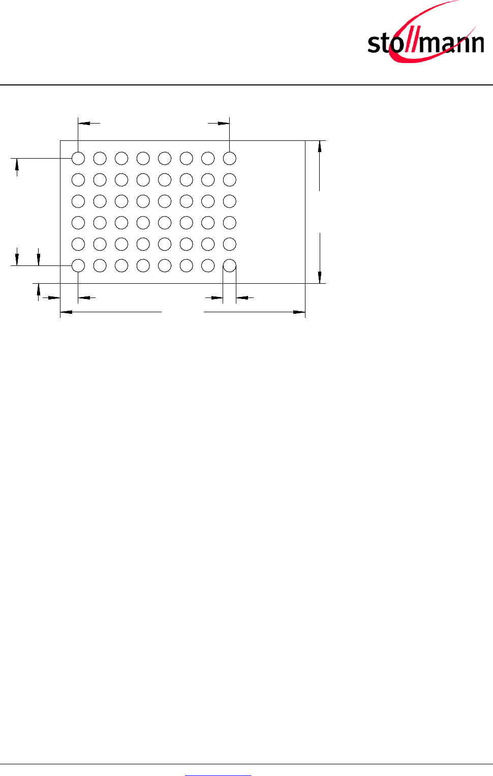
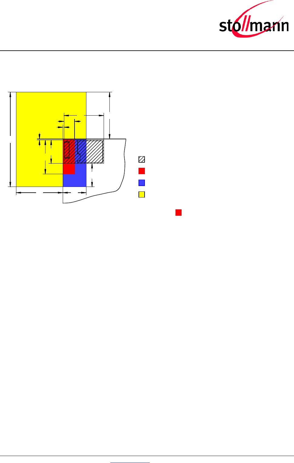
To achieve best radio performance for BlueMod+SR/AI, it is recommended to use the placement
shown in Figure 18.
max.0,5 4,5
10
10
max.0,5
10
15
no bare copper (exept solder pads for module)
no copper and components on any layer
no components on any layer
provide solid ground plane(s) as large as possible around
17
no conductive parts allowed
20
20
40
area
Figure 18: BlueMod+SR/AI Placement Recommendation
6.5 Housing Guidelines
The individual case must be checked to decide whether a specific housing is suitable for the use of
the internal antenna. A plastic housing must at least fulfill the following requirements:
• Non-conductive material, non-RF-blocking plastics
• No metallic coating
• ABS is suggested
6.6 Antenna Issues
BlueMod+SR is shipped with 2 different antenna designs:
• BlueMod+SR/AI comprises a ceramic antenna which as a component is soldered to the
circuit board. This is functional for a BlueMod+SR/AI integrated into a plastic housing. No
additional antenna is required.
For an external antenna to be set in, e.g. because the BlueMod+SR is integrated into a metal
housing, the ceramic antenna is replaced.
• BlueMod+SR/AP routes the antenna signal to pin A-8
The gain of the external antenna shall not exceed +2dBi.
When using an external Antenna the antenna is fixed and cannot be removed or replaced by the
end user. The performance of the internal antenna respectively the external antenna has in any

BlueMod+SR/AI
BlueMod+SR/AP
Hardware Reference
Release r04d01 www.stollmann.de Page 49 of 65
case to be checked within the final integration environment. Adjacent PCBs, components, cables,
housings etc. could otherwise influence the radiation pattern or be influenced by the radio wave
energy.
It must be ensured that the antenna is not co-located or operating in conjunction with any other
antennas, transmitters, cables or connectors. When the internal ceramic antenna is used, certain
restrictions are to be considered.
tbd
6.7 Safety Guidelines
tbd
BlueMod+SR/AI
BlueMod+SR/AP
Hardware Reference
Release r04d01 www.stollmann.de Page 50 of 65
7 Application Diagram
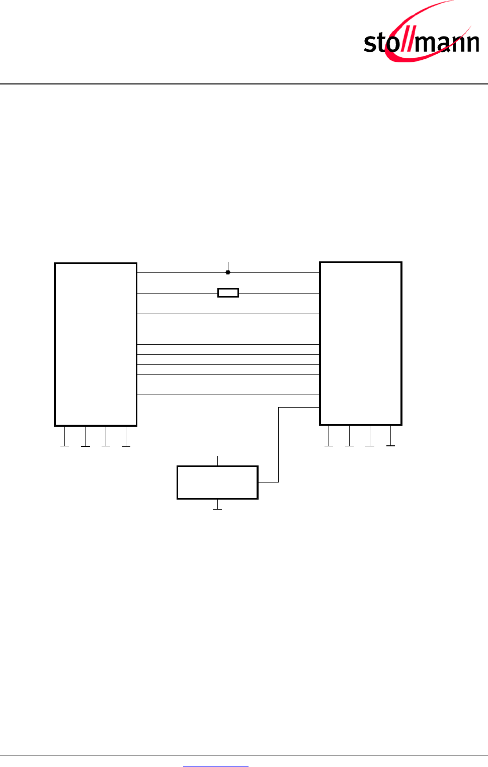
The following schematic shows a typical application of BlueMod+SR. The module is connected to
some MCU running the application layer. MCU and BlueMod+SR use the same 3,3V power
supply. Provisions are made for upgrading the firmware (BOOT0 and EXT-RES# are managed by
the MCU). The serial interface has RTS/CTS flow control but no UICP support in this example. The
Hangup feature to close down the link is provided. As an option to save power, there is an external
slow clock oscillator. All other module pins may be left unconnected.
Host MCU
VDD
GND
+3V3
GPIO (o)
In this example BlueMod+SR is connected to an MCU supporting RTS/CTS flow control and Hangup.
Firmware update is supported (BOOT0, EXT-RES# connected).
The slow clock oscillator (32,768kHz ) is optional; it helps to save power during power down states.
1k
BlueMod+SR/AI
C-1,E-6,F-6 VSUP
GND
B-1 EXT-RES#
BOOT0
GPIO (o)
UART-RXD
UART-TXD
UART-CTS#
UART-RTS#
GPIO[4]/Hangup
TXD (o)
RXD (i)
RTS# (o)
CTS# (i)
GPIO (o)
SLCK
32,768kHz
square
+3V3
The oscillator is optional. Leave A-6 open
or tie to GND if the oscillator is not present.
E-1
D-2
F-4
F-3
D-7
D-4
A-6
all GND pads (14) must be connected.
Blocking capacitors not shown.
pushpull or OD
pushpull
pushpull
Figure 19: Typical Application Schematics

BlueMod+SR/AI
BlueMod+SR/AP
Hardware Reference
Release r04d01 www.stollmann.de Page 51 of 65
8 Approvals/Certifications
The BlueMod+SR/AI has been tested to comply to the appropriate EU, FCC and IC directives. CE
testing is intended for end products only. Therefore CE testing is not mandatory for a Bluetooth
Module sold to OEM’s. Stollmann E+V GmbH provides CE tested Modules for customers in order
to ease CE compliance assessment of end products and to minimize test effort.
8.1 Declaration of Conformity CE
tbd

BlueMod+SR/AI
BlueMod+SR/AP
Hardware Reference
Release r04d01 www.stollmann.de Page 52 of 65
8.2 FCC Compliance
The BlueMod+SR/AI has been tested to fulfill the FCC requirements. Test reports are available on
request. Grants of the Full Modular Approval will be shown below.
For selling products implementing the BlueMod+SR/AP in the USA you’ll have to apply for a Class
II Permissive Change from the FCC authorities. Depending on antenna gain and other factors the
FCC TCB will issue a reduced test plan for re-testing. Stollmann can assist customers with
conducting this procedure on request. Especially the test plan reduction and cost optimization may
be items worth to look at.
8.2.1 FCC Grant
Tbd
FCC Statement
This device complies with 47 CFR Part 2 and Part 15 of the FCC Rules and with.
Operation is subject to the following two conditions:
(1) this device my not cause harmful interference, and
(2) this device must accept any interference received, including interference that may cause
undesired operation.
8.2.3 FCC Caution
Warning: Changes or modifications made to this equipment not expressly approved by Stollmann
Entwicklungs- und Vertriebs- GmbH may void the FCC authorization to operate this equipment.
8.2.4 FCC Warning
This equipment has been tested and found to comply with the limits for a Class B digital device,
pursuant to Part 15 of the FCC Rules. These limits are designed to provide reasonable protection
against harmful interference in a residential installation. This equipment generates, uses and can
radiate radio frequency energy and, if not installed and used in accordance with the instructions,
may cause harmful interference to radio communications. However, there is no guarantee that
interference will not occur in a particular installation. If this equipment does cause harmful
interference to radio or television reception, which can be determined by turning the equipment off
and on, the user is encouraged to try to correct the interference by one or more of the following
measures:
• Reorient or relocate the receiving antenna.
• Increase the separation between the equipment and receiver.
• Connect the equipment into an outlet on a circuit different from that to which the receiver is
connected.

BlueMod+SR/AI
BlueMod+SR/AP
Hardware Reference
Release r04d01 www.stollmann.de Page 53 of 65
Consult the dealer or an experienced radio/TV technician for help.
8.2.5 FCC RF-exposure Statement
The BlueMod+SR/AI complies with the FCC/IC RF radiation exposure limits set forth for an
uncontrolled environment.
The output power is < 10mW e.i.r.p. and therefore according to “FCC KDB 447498 D01 General
RF Exposure Guidance v05” Appendix A, table “SAR Exclusion Threshold”, excluded from SAR
evaluation for test separation distances ≥5mm and if it is not used in co-locations with other
antennas. If the product implementing the BlueMod+SR/AI has other antennas in co-location or
separation distances < 5mm an FCC TCB should be asked for a Class II Permissive Change.
RF exposure evaluation of devices implementing the BlueMod+SR/AP should be done with the
collaboration of the FCC TCB working on the Class II Permissive Change Request.

BlueMod+SR/AI
BlueMod+SR/AP
Hardware Reference
Release r04d01 www.stollmann.de Page 54 of 65
8.2.6 FCC Labeling Requirements for the End Product
Any End Product integrating the BlueMod+SR/AI or /AP must be labeled with at least the following
information:
This device contains transmitter with
FCC ID: RFRMSR
IC: 4957A-MSR

BlueMod+SR/AI
BlueMod+SR/AP
Hardware Reference
Release r04d01 www.stollmann.de Page 55 of 65
8.3 IC Compliance
The BlueMod+SR/AI has been tested to fulfill the IC requirements. Test reports RSS-210 of
Industry Canada are available on request. Grants of the Full Modular Approval will be shown
below.
For selling products implementing the BlueMod+SR/AP in Canada you’ll have to apply for a Class
II Permissive Change from the IC authorities. Depending on antenna gain and other factors the IC
TCB will issue a reduced test plan for re-testing. Stollmann can assist customers with conducting
this procedure on request. Especially the test plan reduction and cost optimization may be items
worth to look at.
8.3.1 IC Grant
tbd

BlueMod+SR/AI
BlueMod+SR/AP
Hardware Reference
Release r04d01 www.stollmann.de Page 56 of 65
8.3.2 IC Statement
(i) Ce dispositif doit être installé et exploité dans une enceinte entièrement fermée afin de prévenir
les rayonnements RF qui pourraient autrement perturber la navigation aéronautique. L’installation
doit être effectuée par des installateurs qualifiés, en pleine conformité avec les instructions du
fabricant.
(ii) Ce dispositif ne peut être exploité qu'en régime de non-brouillage et de non-protection, c’est-à-
dire que l’utilisateur doit accepter que des radars de haute puissance de la même bande de
fréquences puissent brouiller ce dispositif ou même l’endommager. D’autre part, les capteurs de
niveau à propos desquels il est démontré qu’ils perturbent une exploitation autorisée par licence de
fonctionnement principal doivent être enlevés aux frais de leur utilisateur.
This device complies with Industry Canada license-exempt RSS standard(s).
Operation is subject to the following two conditions:
(1) this device may not cause interference, and
(2) this device must accept any interference, including interference that may cause undesired
operation of the device.
NOTICE:
This Class B digital apparatus complies with Canadian ICES-003.
Cet appareil numérique de la classe B est conforme à la norme NMB-003 du Canada.
8.3.3 IC Caution
Warning: Changes or modifications made to this equipment not expressly approved by Stollmann
Entwicklungs- und Vertriebs-GmbH may void the IC authorization to operate this equipment.
8.3.4 IC RF-exposure Statement
This equipment is portable device. The output power of this device is less than 20mW.
The SAR test is not required.
RF exposure evaluation of devices implementing the BlueMod+SR/AP should be done with the
collaboration of the IC TCB working on the Class II Permissive Change Request.

BlueMod+SR/AI
BlueMod+SR/AP
Hardware Reference
Release r04d01 www.stollmann.de Page 57 of 65
8.3.5 IC Labeling Requirements for the End Product
Any end product integrating the BlueMod+SR/AI or /AP must be labeled with at least the following
information:
This device contains transmitter with
FCC ID: RFRMSR
IC: 4957A-MSR
8.3.6 IC Label Information BlueMod+SR
The BlueMod+SR shows no IC-ID on the product label, because there is no space available. IC
allows on request to state the IC-ID in the product manual. This product has been granted to do so.
The IC-ID is: 4957A-MSR

BlueMod+SR/AI
BlueMod+SR/AP
Hardware Reference
Release r04d01 www.stollmann.de Page 58 of 65
8.4 Bluetooth Qualification
The BlueMod+SR is a qualified design according to the Bluetooth Qualification Program Reference
Document (PRD) V2.1. The Qualified Design ID (QDID) is:
tbd
For further information about marking requirements of your product attention should be paid the
Bluetooth Product Marking Guide at
https://www.bluetooth.org/Download/Marking_Guide_20060601.pdf
According to the Bluetooth SIG rules (Qualification Program Reference Document – PRD V2.1)
you are required to perform the mandatory End Product Listing (EPL) for your product. For further
information see www.Bluetooth.org or contact Stollmann.

BlueMod+SR/AI
BlueMod+SR/AP
Hardware Reference
Release r04d01 www.stollmann.de Page 59 of 65
8.5 RoHS Declaration
Declaration of environmental compatibility for supplied products:
Hereby we declare to our best present knowledge based on declaration of our suppliers that this
product do not contain by now the following substances which are banned by Directive 2011/65/EU
(RoHS 2) or if contain a maximum concentration of 0,1% by weight in homogeneous materials for
• Mercury and mercury compounds
• Chromium (VI)
• PBB (polybrominated biphenyl) category
• PBDE (polybrominated biphenyl ether) category
• And a maximum concentration of 0,01% by weight in homogeneous materials for
• Cadmium and cadmium compounds
9 Related Documents
[1] CD00171190.pdf Oct. 2011 Rev 14 (STM32_Reference)
[2] CD00191185.pdf April 2011 Rev 8 (STM32_datasheet)
[3] Stollmann: UICP_UART_Interface_Control_Protocol_r01.pdf
[4] Stollmann: AppNote_B0601_Antenna_Design_V1_0.pdf
[5] Stollmann: BlueMod+SR AT Command Reference
[6] Stollmann: BlueMod+SR_Startup_Timing_r01.pdf
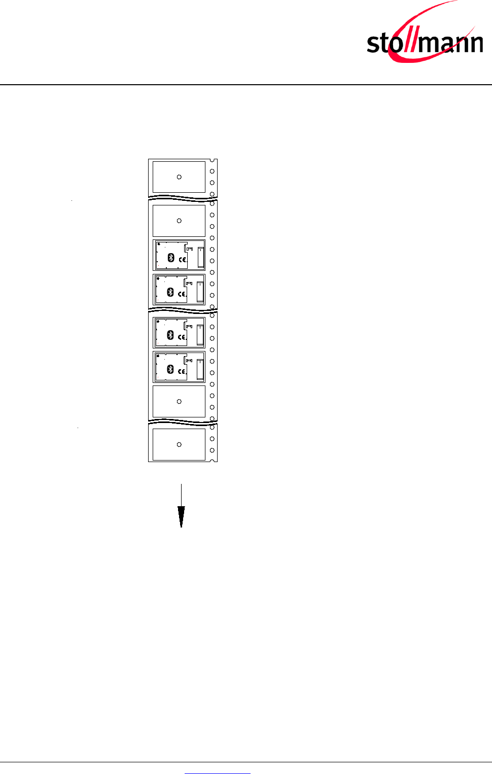
BlueMod+SR/AI
BlueMod+SR/AP
Hardware Reference
Release r04d01 www.stollmann.de Page 60 of 65
10 Packing
The BlueMod+SR modules are packed using carrier tape.
Abzugrichtung von der Rolle/
pull off direction from reel
FCC ID RFRMSR
stollmann
BlueMod+SR
FCC ID RFRMSR
stollmann
BlueMod+SR
25 Leertaschen Vorspann pro Verpackungseinheit/
25 empty pockets as leader per packing unit
15 Leertaschen Nachspann pro Verpackungseinheit/
15 empty pockets as trailer per packing unit
FCC ID RFRMSR
stollmann
BlueMod+SR
FCC ID RFRMSR
stollmann
BlueMod+SR
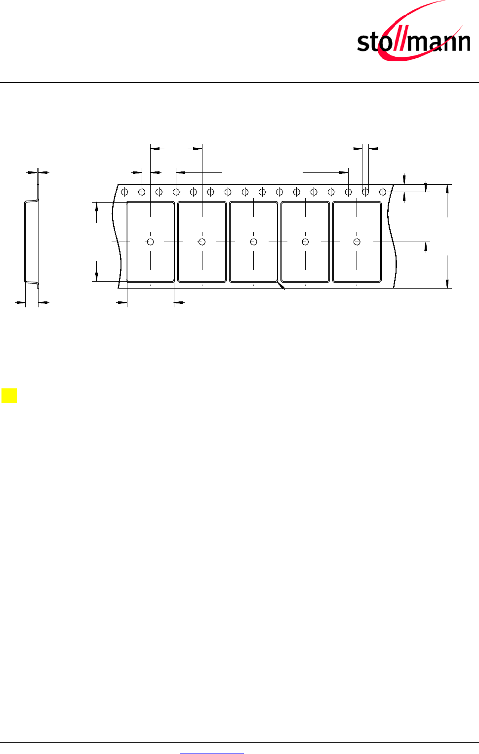
BlueMod+SR/AI
BlueMod+SR/AP
Hardware Reference
Release r04d01 www.stollmann.de Page 61 of 65
10.1 Tape
The dimensions of the tape are shown in the drawing below (values in mm):
2,0
+0,1
-0,1
10,9
+0,1
-0,1
18,3
+0,1
-0,1
R 0,5
1,75
+0,10
-0,10
24,0
+0,3
-0,3
10x4,0=40,0
+0,2
-0,2
1,5
+0,1
-0,0
12,0
11,5
+0,1
-0,1
0,3
3,0
10.2 Reel
tbd
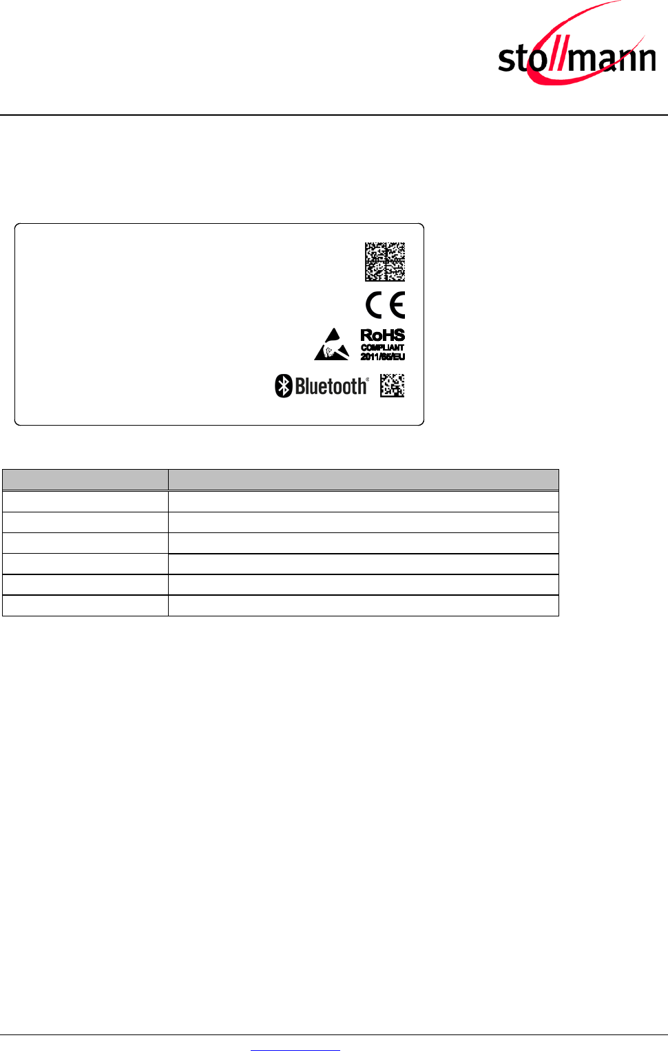
BlueMod+SR/AI
BlueMod+SR/AP
Hardware Reference
Release r04d01 www.stollmann.de Page 62 of 65
Label Information
10.3 Package Label
Package box, dry shield bag and reel are each marked with the following label:
Stollmann E+V GmbH
name
p/n
firmware
fw p/n
trace
quantity
bundle
designed and manufactured in Germany
BlueMod+SR/Ax
xxxxx-yy
SR/Vx.xxx
Mwwyy
q
BNDLxxxxxxxxxxxx
Field
Description
name Name of product
p/n Product number
firmware Firmware version
fw p/n Product number of firmware
trace [Manufacturer M (optional)]Date (YearCalendarWeek) YYWW
quantity Number of contained modules
If the label on the package box is different to the label described please contact Stollmann for
detailed information.
BlueMod+SR/AI
BlueMod+SR/AP
Hardware Reference
Release r04d01 www.stollmann.de Page 63 of 65
11 Ordering Information
11.1 Part Numbers
BlueMod+SR is available in the following variants:
Name Antenna Order No. MOQ /
units Comments
BlueMod+SR/AI internal 53231-xx 50
BlueMod+SR/AP external 53252-xx 500
BlueEva+SR Internal 53249-xx 1 Evaluation Kits
Other variants on request, please contact Stollmann sales department.
11.2 Standard Packing Unit
The standard packing unit is 500 pieces Tape and Reel
11.3 Evaluation Kit
The kit BlueEva+SR is available to evaluate functionality and start your firmware implementation.

BlueMod+SR/AI
BlueMod+SR/AP
Hardware Reference
Release r04d01 www.stollmann.de Page 64 of 65
History
Version Release Date By Change description
r02 04.02.2013 MW/JW First preliminary release
r03
21.02.2013
MW/GJ
GJ
JW
FH
signal naming conventions harmonized
signals in tables re-sorted
corrected some typos
updated dimension drawing (with new antenna)
added land pattern drawing
renamed chapter “Restricted Area” into “Placement Recommendation” and
replaced text with drawing
Figure 10 “Pin Numbering” added
Added current consumption for standby mode
Chapter 1 Introduction revised
r04d01 22.02.2013
06.03.2013
19.04.2013 ff.
JW
MW
Spelling and formatting
Chapter 3, Application Examples added to several sub chapters
Chapter 3.1 Power Supply, requirements lowered
Chapter 3.3 allowed to use series resistor to connect external low-active reset
Chapter 3.5 Serial Interface updated, UICP included
Chapter 3.6 renamed to GPIO Interface
Chapter 3.10 minor changes in text
Enhanced chapter 3.13 Pin Strapped System Memory Boot Mode Invocation
New chapter 3.15 Serial Wire Interface
Chapter 4.2 Pin Description, tables updated and corrected, removed signals
“/BT-CONNECTED” and “STM32-WAKEUP”
New chapter 4.3 Handling of unused Signals
Chapter 5.6 Power Consumption Tables updated
Chapter 5.7 RF parameter updated
Chapter 5.7.5 Antenna Gain and Radio Pattern updated
Chapter 6.3 updated
New chapter 7 Application Diagram

