Ten Tec 400 HF/VHF/UHF RECEIVER User Manual RX400 Manual Version 0 5
Ten Tec Inc HF/VHF/UHF RECEIVER RX400 Manual Version 0 5
UserManual.wiki
>
Ten Tec
>
400 User Manual
Users Manual
Navigation menu
Upload a User Manual
Namespaces
Wiki Guide
HTML
PDF
Info
Views
User Manual
Discussion / Help
Navigation

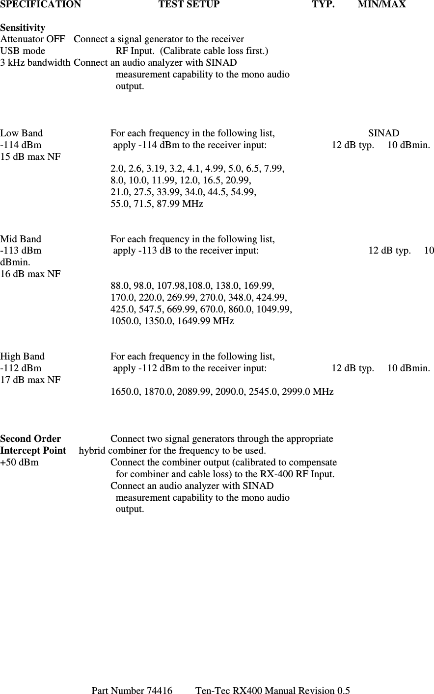
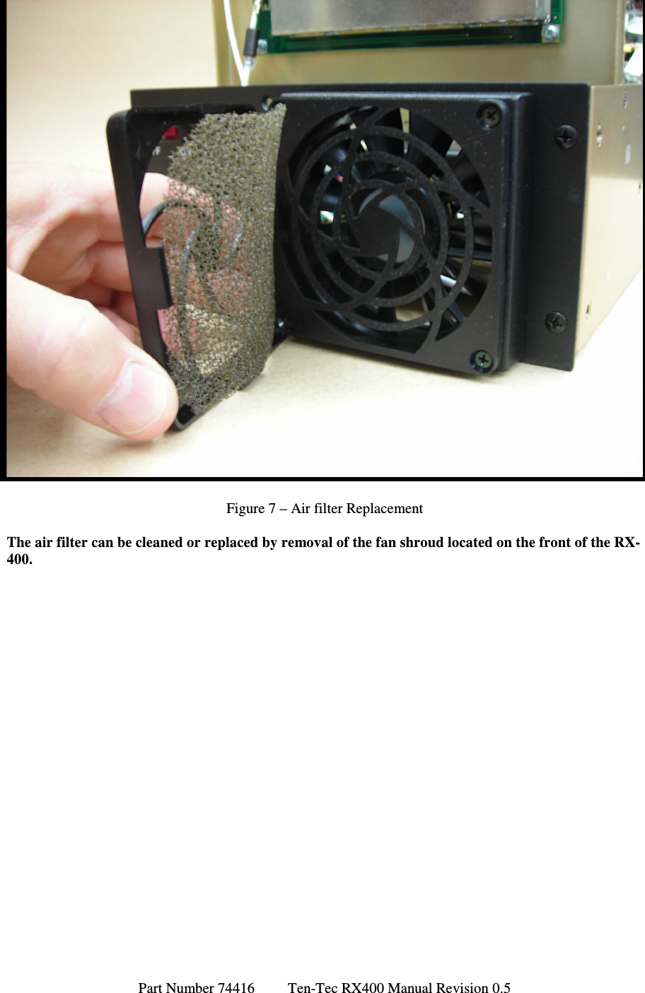
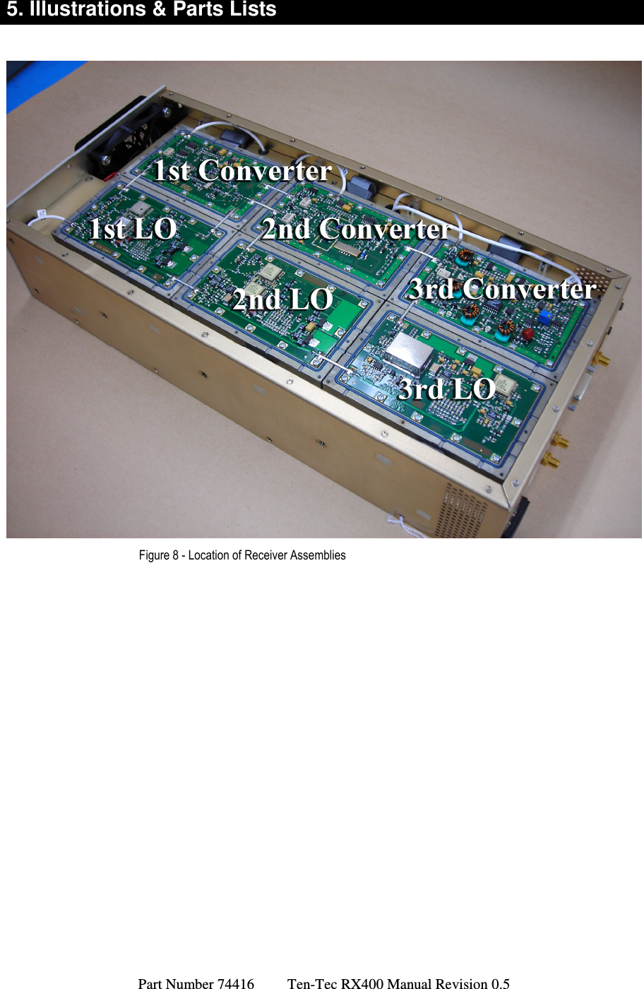
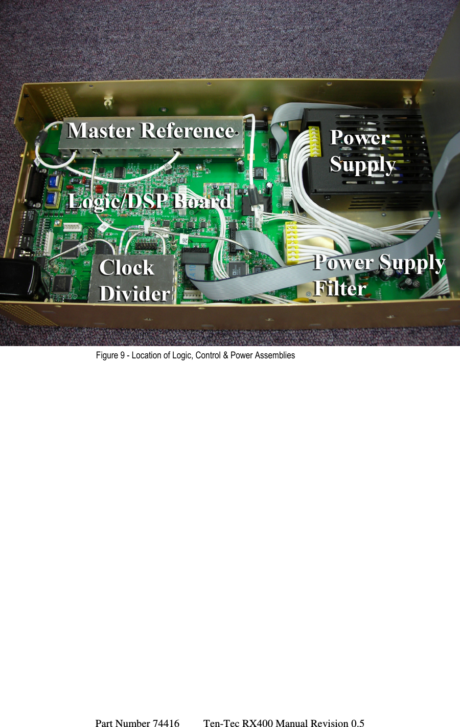
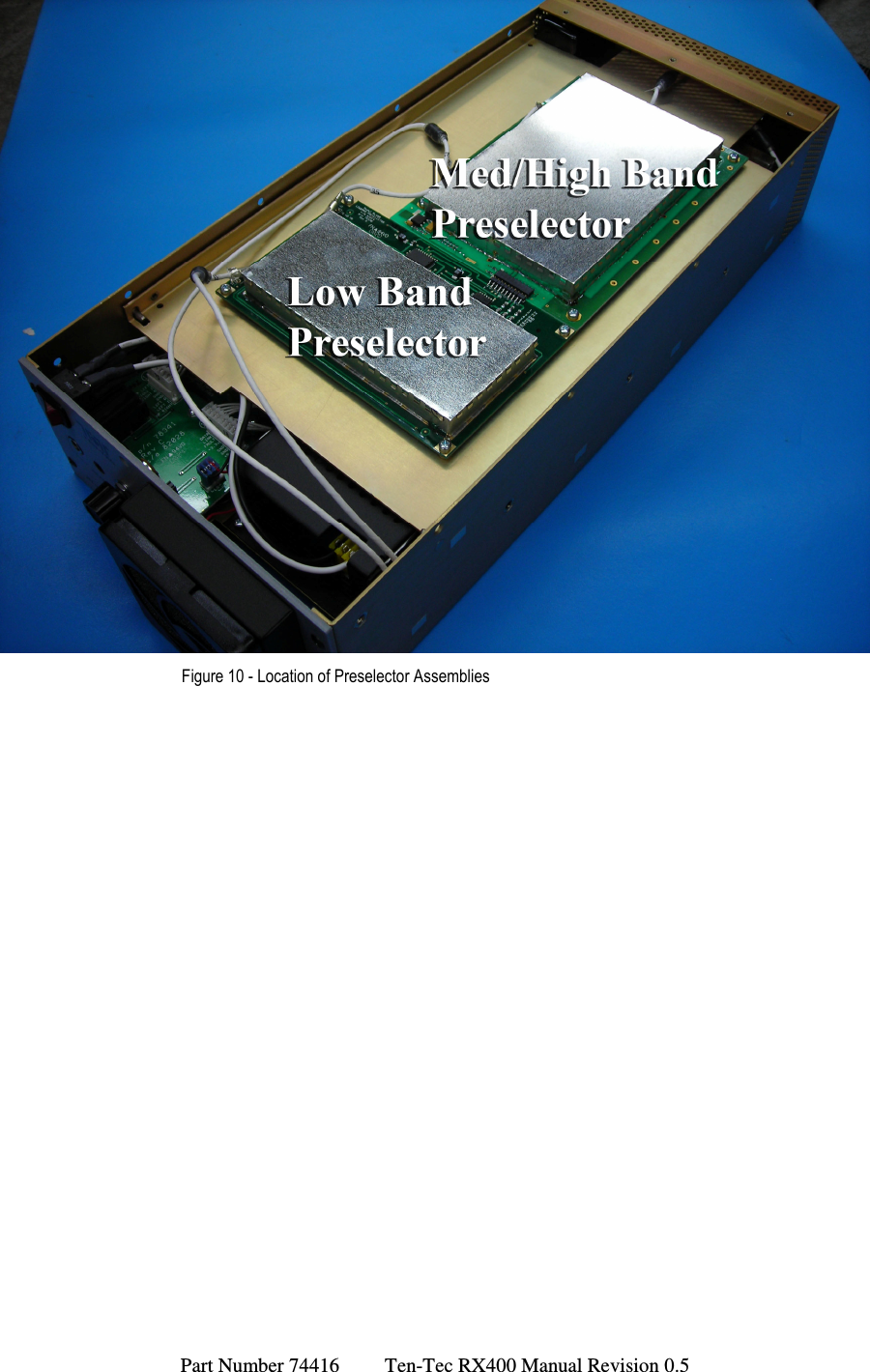
![Part Number 74416 Ten-Tec RX400 Manual Revision 0.5 SPECIFICATION TEST SETUP TYP. MIN/MAX For each frequency in the list below: Temporarily set generator #1 on frequency to supply a level of -110 dBm to the receiver input. Record the SINAD displayed on the audio analyzer as "reference". Move generator #1 to (frequency / 2) -9 kHz. Set generator #2 to (frequency / 2) +9 kHz. Set both generator amplitudes to produce -30 dBm each at the receiver input connector. Observe the SINAD of the second order distortion product on the audio analyzer. Calculate the Second Order Intercept as: 50 +(ref. SINAD) -(dist. prod. SINAD) 55 dBm typ. 50 dBm min. 3.19, 4.99, 7.99, 11.99, 20.99, 33.99, 54.99, 87.99, 107.98, 169.99, 269.99, 424.99, 669.99, 1049.99, 1649.99, 2089.99, 2999.0 MHz Third Order Connect two signal generators through the appropriate Intercept Point hybrid combiner for the frequency to be used. -7 dBm Connect the combiner output (calibrated to compensate for combiner and cable loss) to the RX-400 RF Input. Connect a spectrum analyzer to the RX-400 21.4 MHz IF output. Using the frequencies listed above for the Second Order test: Set generator #1 to frequency -10 kHz. Set generator #2 to frequency +10 kHz. Set both generator amplitudes to each produce -20 dBm at the receiver input connector. If the third order products displayed on the spectrum analyzer have amplitudes that are equal or within 6 dB, use their average amplitude to calculate the Third Order Intercept as: {[(tone level) - (dist. prod. level)] / 2 } -20 -5 dBm typ. -7 dBm min. If the distortion products differ by more than 6 dB, use the higher level product in the calculation.](https://usermanual.wiki/Ten-Tec/400/User-Guide-1049140-Page-16.png)