Texas Instruments 2531NANO The CC2531NANO is a miniaturized USB dongle for ZigBee® RF4CE applications. User Manual RemoTI Development Kit Users Guide
Texas Instruments Inc. The CC2531NANO is a miniaturized USB dongle for ZigBee® RF4CE applications. RemoTI Development Kit Users Guide
User Manual
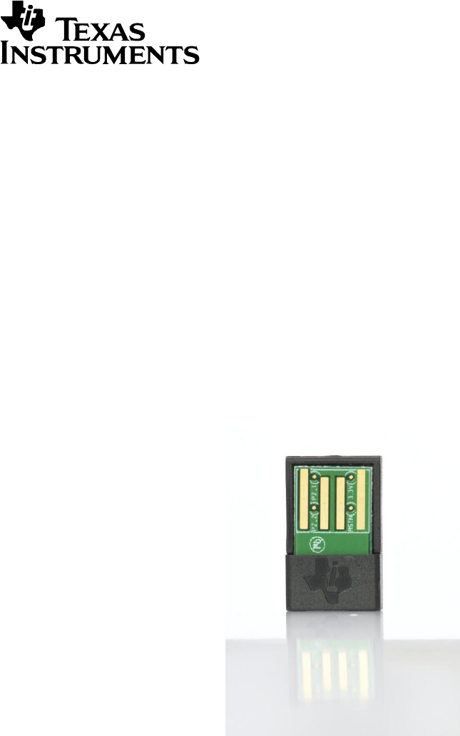
CC2531 NANO USB stick
User’s Guide

2/21
Table of Contents
1 INTRODUCTION ...................................................................................................................... 4
2 ACRONYMS AND ABBREVIATIONS ................................................................................... 5
3 HW REQUIREMENTS ............................................................................................................. 6
4 NANO USB STICK SERIAL BOOT LOADER ...................................................................... 7
4.1 SOFTWARE REQUIRED .................................................................................................................... 7
4.2 SBL BOOT CODE IMAGE ............................................................................................................... 8
4.3 DOWNLOAD THE SERIAL BOOTLOADER ....................................................................................... 8
4.4 SBL COMPATIBLE APPLICATION CODE IMAGE .............................................................................. 9
4.5 GENERATING A BINARY FILE:........................................................................................................ 9
4.5.1 Note on the batch files: ............................................................................................................................................... 13
4.5.2 Modify the code placement: ........................................................................................................................................ 13
4.6 DOWNLOAD A NEW APPLICATION IMAGE VIA SBL ..................................................................... 14
4.6.1 Serially boot the new Application Image (binary file): ................................................................................................... 14
4.6.2 Remark about the Application .................................................................................................................................... 15
4.7 COMMON ISSUES ........................................................................................................................ 15
4.7.1 SmartRF Programmer bug: ........................................................................................................................................ 15
4.7.2 USB Driver issues: ....................................................................................................................................................... 15
5 SCHEMATIC AND LAYOUT ................................................................................................ 15
6 DOCUMENT HISTORY ......................................................................................................... 15


4/21
1 Introduction
The NANO USB stick is a miniature USB interface for 2.4GHz wireless applications. The design is
based on a CC2531 System-on-Chip with an IEEE 802.15.4 radio. The NANO USB stick supports
ZigBee and RF4CE applications. Typical applications includes:
ZigBee RF4CE USB HID(Human Interface Device)
ZigBee RF4CE serial port interface
ZigBee gateway and commisioning interface for PC
The NANO USB stick simplifies development of USB interface for ZigBee and RF4CE applications.
The small and low cost design allows integration of ZigBee and RF4CE into PCs, Set-Top boxes,
TVs, tablets and smart phones. The NANO USB stick provides an easy integration of ZigBee and
RF4CE radios into all types of electronics with USB interface
The since the NANO USB stick is FCC/ETSI certified you can use the product with full confidence that
the product will pass certification and significantly reduce design times. For customers that want to
make their own products the reference design files are available upon request.

5/21
2 Acronyms and Abbreviations
LED
Light Emitting Diode
LPW
Low Power Wireless
MCU
Micro Controller
RF
Radio Frequency
RF4CE
Radio Frequency for Consumer Electronic
SoC
System on Chip
TI
Texas Instruments
USB
Universal Serial Bus
6/21
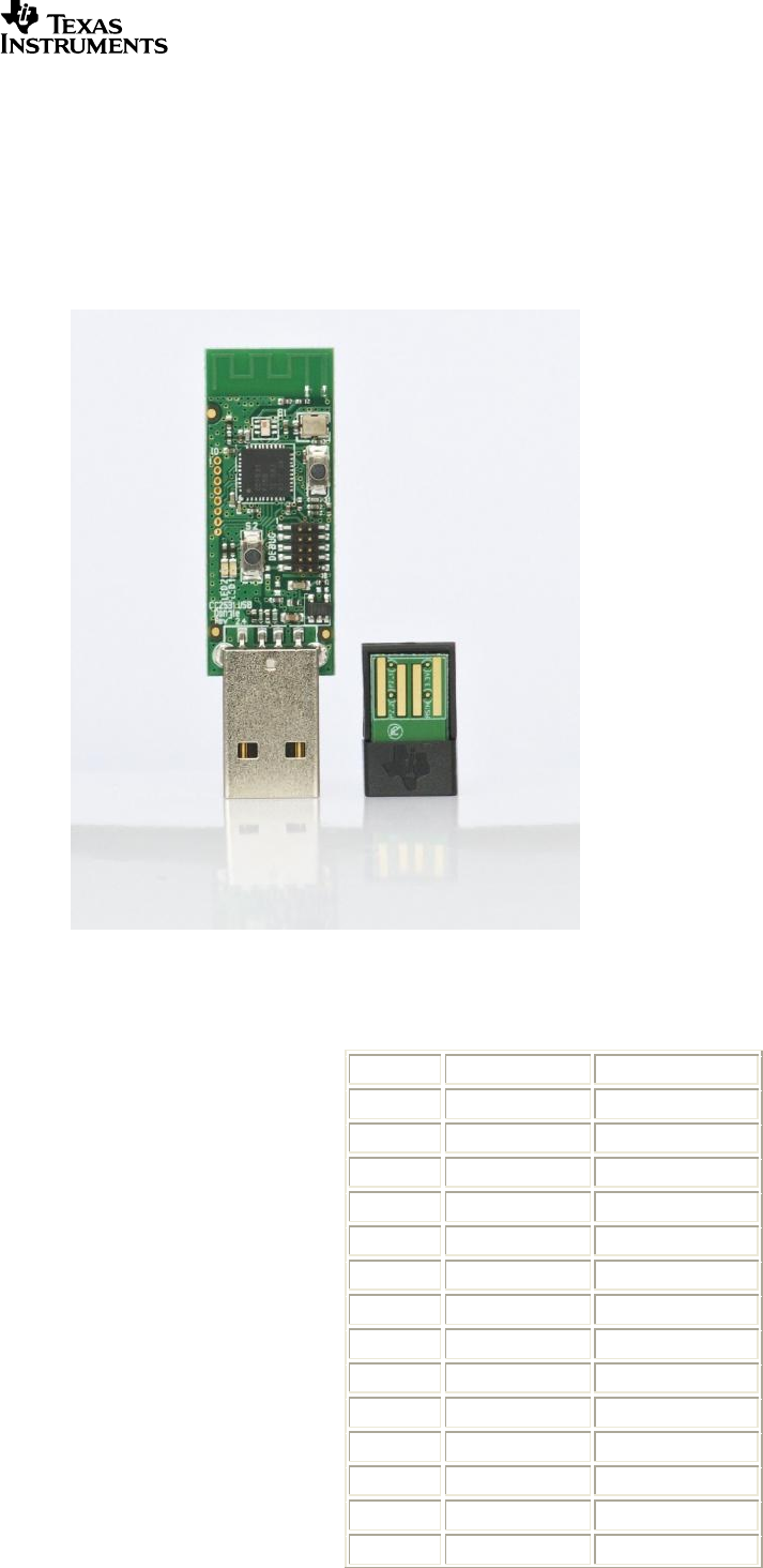
3 HW requirements
Since the NANO USB stick has no I/O connections or LEDs for user interface it is recommended to
use a standard CC2531 USB dongle for SW development and prototyping before loading the code
onto the NANO USB stick. The NANO USB stick is compatible with regards to USB interface and
radio interface to the standard CC2531 USB dongle.
Figure 1: NANO USB stick and standard USB stick
The table below lists the difference in I/O pin connections between the NANO USB stick and the
CC2531 USB dongle
Pin name
CC2531 dongle
NANO USB stick
P0_0
LED
GND
P0_1
Not connected
GND
P0_2
I/O Pin header
GND
P0_3
I/O Pin header
GND
P0_4
I/O Pin header
GND
P0_5
I/O Pin header
GND
P0_6
Not connected
GND
P0_7
Not connected
GND
P1_0
USB pull-up
USB pull-up
P1_1
LED
GND
P1_2
Push button
GND
P1_3
Push button
GND
P1_4
I/O Pin header
GND
P1_5
I/O Pin header
GND
7/21
P1_6
I/O Pin header
GND
P1_7
I/O Pin header
GND
P2_0
Not connected
GND
P2_1
Debug data
Debug data
P2_2
Debug clock
Debug clock
P2_3
Not connected
GND
P2_4
Not connected
GND
Table 1: NANO USB and standard USB pin assignments
The debug interface on the NANO USB stick is accessible on test points between the USB connector
pins but these test points are small and difficult to access. Hence it is recommended to use the USB
bootloader code programmed into the device for loading application code onto the device.
All unused I/Os should be configured as input pull-down at the beginning of your application to reduce
current consumption.
4 NANO USB Stick Serial Boot Loader
This section will guide you through the steps needed to build a Serial Boot Loader (SBL) for a Z-stack
and for an RF4CE application and will explain you how to modify such an application to be compatible
with the SBL. The SBL is provided as a value-enhancing sample solution that enables the updating of
code in devices without the cost of maintaining any download-related code in the user application
other than ensuring a compatible flash memory mapping of the final output. SBL is effected as a
managed client-server mechanism which requires a serial master to drive the process (i.e. a PC GUI
application with access to the serial connection to the CC2531.)
Since the NANO USB stick has no human interface such as keys, the boot loader will always
automatically start before the application, wait for a potential application downloading during ~15sec,
and then automatically jump to the application if any valid image is already loaded in flash. If not, it will
wait for an application downloading forever.
Therefore, when the SBL will be loaded into flash memory, each time you connect your NANO USB
stick into a USB port you will have around 15 seconds to download your new application. Then the
SBL will jump to the existing application and you won’t be able to download your new application
anymore.
The following sections will walk you through the steps needed to build and download the SBL, then
build and download an SBL compatible application using IAR to finally load your application on the
NANO USB stick using SBDemo tool.
4.1 Software required
File name
Description
Link
Bootloader_xxx.hex
Bootloader hex file
Wiki ZIP
archive : File:NANO-
USB package.zip
SBDemo
Serial Bootloader PC interface
demo application, used to load
binary files with the bootloader
znp.bat, znp.js, sim2bin.exe for a Z-
stack application
pp_cc2531f256sb.bat, oadbbin.exe
for a RemoTI stack application
scripts and executable files
performing file conversion
8/21
Linker_xxx.xcl
Linker file
usb_cdc_driver_cc2531_PID16B2.inf
usb_cdc_driver_cc2531_PID16A8.inf
USB drivers
Z-stack ZNP Applications Example
ZigBee Network Processor
application example, based on
the Z-stack ZNP project
http://focus.ti.com/docs/t
oolsw/folders/print/z-
stack.html
RF4CE RNP Application Example
ZigBee Remote Network
Processor(RNP) application
example, based on the RemoTI
RNP project
http://focus.ti.com/docs/t
oolsw/folders/print/remo
ti.html
Texas Instruments SmartRF Flash
Programmer
Flash Programmer PC tool, used
to program hex files using
debuggers
http://focus.ti.com/docs/t
oolsw/folders/print/flash-
programmer.html
- Tools - znp.bat, znp.js, sim2bin.exe for a Z-stack application (automatically installed with the Z-stack
in \Projects\zstack\ZNP\CC253x\tools
- pp_cc2531f256sb.bat, oadbbin.exe for a RemoTI stack application (automatically installed with the
RemoTI stack under, respectively, \Projects\RemoTI\RNP\CC2530EB and
Projects\RemoTI\common\cc2530
- Linker files: cc2530-sb.xcl (Z-stack), ti_51ew_cc2531f256_sb.xcl (RemoTI). These linker files are
automatically installed with the Z-stack and the RemoTI stack under, respectively,
\Projects\zstack\Tools\CC2530DB and \Projects\RemoTI\common\cc2530
- USB Drivers (usb_cdc_driver_cc2531_PID16B2.inf and usb_cdc_driver_cc2531_PID16A8.inf)
4.2 SBL Boot Code Image
If the SBL is already loaded on your target, skip this section.
This section will guide you through the steps needed to program the Bootloader image into flash using
Texas Instrument SmartRF Programmer. The project for the boot image already exists, so all you
need to do here is open the project, rebuild it and download the output .hex file with SmartRF
Programmer.
But before downloading the SBL, you may want to tune the period during which the SBL waits for an
application to be downloaded (it happens after powercycling the device, the default setting is around
15 sec). To do that, just modify the SBL_WAIT_PERIOD value defined in the Constants section in the
main file of the SBL project, called either sb_main.c for the Z-stack bootloader, or main_cc2531.c for
the RemoTI stack. This waiting period is not implemented with timers, it simply uses a while loop
statement decrementing the SBL_WAIT_PERIOD value. This value is initialized to a non-zero value,
and when it reaches zero the SBL jumps to the application. Therefore the conversion between the
variable value and corresponding time is approached by the relation:
For Z-stack SBL : SBL_WAIT_PERIOD = 21 845 * X, where X is the waiting period in seconds.
For RemoTI SBL : SBL_WAIT_PERIOD = 23 130 * X, where X is the waiting period in seconds.
Modify the value and rebuild the project. Then you can download the SBL on the target.
4.3 Download the Serial Bootloader
1. Open Texas Instruments SmartRF Programmer
2. SelectProgram CCxxxx SoC or MSP430 under What do you want to program ?
3. Select System-on-chip tab
4. Browse the Flash image field to the .hex object file of the SBL
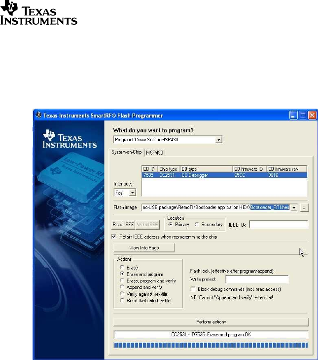
9/21
5. First Erase the flash by selecting Erase in Actions and then click Perform Actions
6. Then program the flash by selececting Erase and Program or Erase, program and verify, then
click Perform actions.
4.4 SBL Compatible Application Code Image
In this section you will be guided through the steps needed to convert an already existing Z-Stack
2.4.0 or RemoTI 1.2.1 application (in this case the RemoTI RNP application and, in parallel, the Z-
stack ZNP application) into one that is compatible with the SBL. The application needs to be modified
such that it does not overwrite the SBL that has been programmed into flash in the previous section.
After the project has been modified to be SBL compatible the final steps in this section will program
the SBL compatible application into flash using SBDemo.
4.5 Generating a Binary file:
The project must be modified to produce a binary file that can be downloaded by the SBL PC
Application “SBDemo.exe”. This will be used in later sections.
In IAR, open your project, here we will use RNP and ZNP projects:
1. File->Open->Open workspace
2. Browse to and open
a. for the Z-Stack: " Projects\zstack\ZNP\CC253x\ znp.eww "
b. for the RemoTI stack: “Projects\RemoTI\RNP\CC2530EB\ rnp_cc2530.eww”
3. From the project view in Left panel click on the drop down box at the top
4. Select
a. For the Z-stack: “CC2531 – ProdSBL”
b. For the RemoTI stack: “CC2531F256_SB”
5. Project->Options
6. Select "Build Actions" category in left panel
7. Depending on the stack you will use, different tools will be used to generate a binary file:
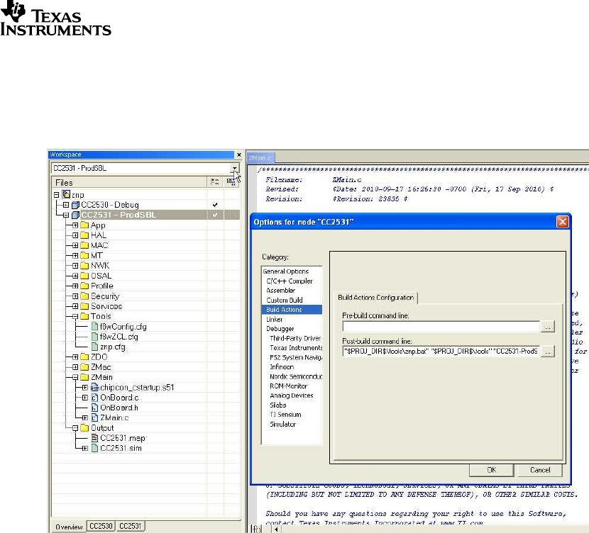
10/21
a. For the Z-stack: Add the following line to the "Post-build command line":
"$PROJ_DIR$\tools\znp.bat" "$PROJ_DIR$\tools" "CC2531-ProdSBL"
b. For the RemoTI stack:Add the following line to the "Post-build command line":
"$PROJ_DIR$\pp_cc2531f256sb.bat" "$PROJ_DIR$"
8. Now select "Linker" category in the left panel
a. For the Z-stack : in the Ouput tab, in the Format section, select Other, then Output Format:
simple-code and Format variant: None
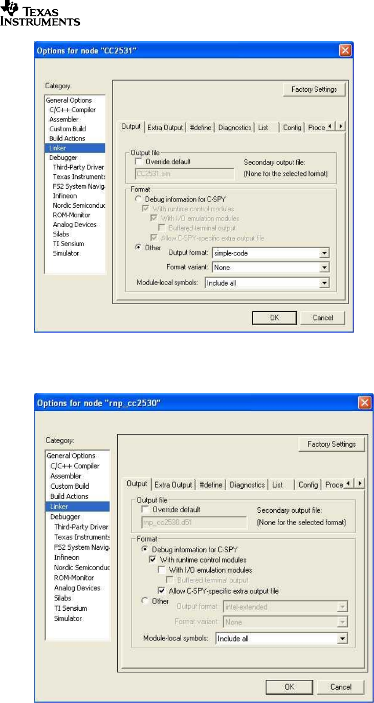
11/21
b.1) For the RemoTI stack : in the Output tab, in the Fornat Section, select Debug information for
C-SPY, and check "With runtime control modules" and "Allow C-SPY - specific extra ouput file"
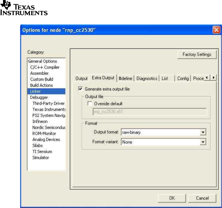
b.2) in the Extra Ouput tab, check Generate extra ouput file and in the Format section
select Ouput format : raw-binary and Format variant : None
12/21
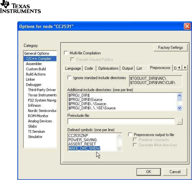
9. For the Z-stack-based ZNP project only:
a. Select "C/C++ Compiler" category in left panel
b. Select "Preprocessor" tab in right panel
c. At the bottom of the "Defined Symbols: (one per line)" list add (on a new line)
MAKE_CRC_SHD (it resets the CRC located at 0x2092-0x2093 in CODE to 0xFFFF value)
13/21
4.5.1 Note on the batch files:
znp.bat and pp_cc2531f256sb.bat use tools located in different directories, therefore be careful to
respect the proper location of your files:
znp.bat : calls znp.js which shall be located in "$PROJ_DIR$\tools" (1st option of znp.bat) where
$PROJ_DIR$ refers to your project directory containing znp.eww. znp.js usessim2bin.exe wich
actually converts a .sim file into a .bin file. The .sim file is an output of IAR, sim2bin.exe fetches it in
the "CC2531-ProdSBL" (2nd option of znp.bat) directory located in the project directory. Ensure that
all the files and directories are properly located and named.
pp_cc2531f256sb.bat : calls oadbbin.exe located in "$PROJ_DIR$\..\..\common\cc2530\”, where one
“..\” means one on-directory. oadbbin.exe uses rnp_cc2531.a51 (ouput of IAR) located in
"$PROJ_DIR$\CC2531F256_SB\Exe\” and creates rnp_cc2531.bin located in
"$PROJ_DIR$\CC2531F256_SB\Exe\”. Ensure that all the files and directories are properly located
and named.
This remark holds for the linker file location, cf. below.
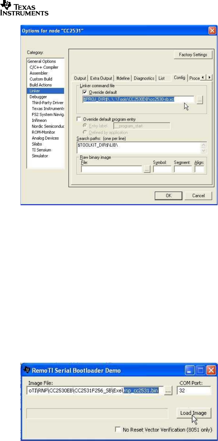
4.5.2 Modify the code placement:
The SBL resides in the beginning of flash. So the linker command file needs to place the application
image in an area of memory that does not overlap the SBL (and further more at a start address
expected by the SBL).
1. On the left pannel select Linker
2. Select "Config" tab.
3. Change the linker command file to:
a. For the Z-stack: $PROJ_DIR$\..\..\Tools\CC2530DB\cc2530-sb.xcl
b. For the RemoTI stack: $PROJ_DIR$\..\..\common\cc2530\ti_51ew_cc2531f256_sb.xcl
4. Rebuild your project.
14/21
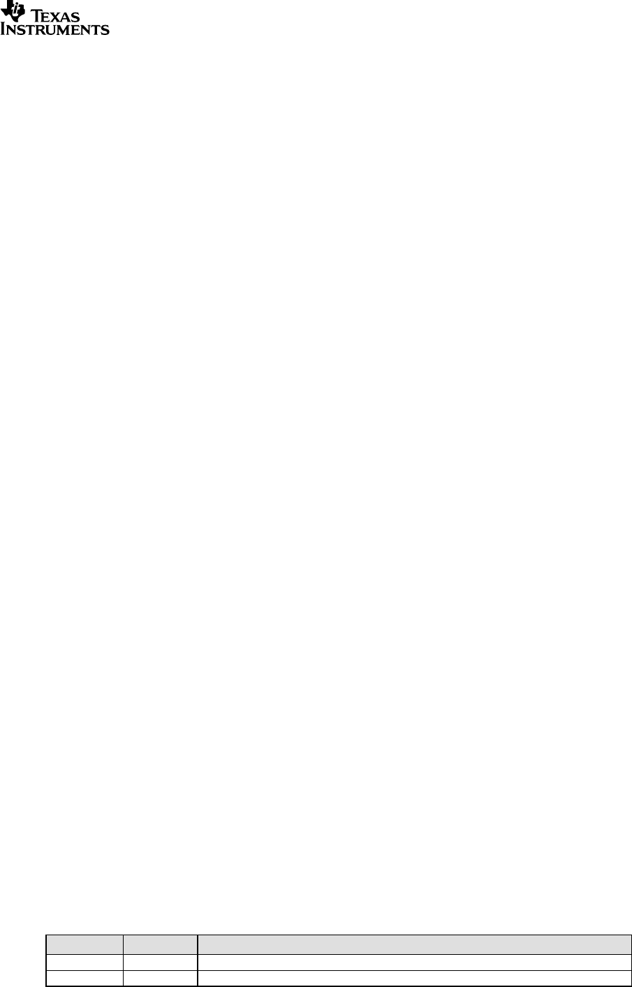
4.6 Download a New Application Image via SBL
Once an SBL compatible binary file has been generated, you can download it on the NANO USB stick
using the SBDemo tool.
4.6.1 Serially boot the new Application Image (binary file):
1. Connect the NANO USB stick into a USB port
2. Open SBDemo.exe
3. Click on the “...” button and browse to your application image, ex:
a. For the Z-stack: “Projects\zstack\ZNP\CC253x\dev\ CC2531ZNP-Prod.bin”
b. For the RemoTI stack: “Projects\RemoTI\RNP\CC2530EB\CC2531F256_SB\Exe\
rnp_cc2531.bin”
4. Click on the Open button.
5. Enter the COM Port of the SBL (cf. Device Manager)
6. Click on the "Load Image" button to send the file.
7. The file will take a couple of seconds to download and verify.
8. Power cycle the NANO USB stick
15/21
4.6.2 Remark about the Application
The NANO USB stick dongle has almost* all of its pins connected to ground; therefore you should set
these pins to be input pull-down at the beginning of your application to reduce current consumption.
After a reset the default state is input pullup for all GPIOs.
* Port0, Port1 and I/O 2.0, 2,3, 2.4
4.7 Common Issues
4.7.1 SmartRF Programmer bug:
Sometimes the SmartRF Programmer window gets out of the screen so you can’t see it anymore but
it is still present in the task bar. Therefore you just need to move the window back into the screen:
1. Left click on the application in the task bar to select it
2. Right click on the application in the task bar
3. Click on Move
4. Hit any array button (up/down/left right) on your keyboard to enable the Move command
5. Move your mouse until you see the smart RF window appear on your screen.
4.7.2 USB Driver issues:
When you connect a NANO USB stick for the first time in a USB port, Microsoft Windows may
automatically install the corect driver. If it does, you should then see your NANO USB stick appear in
the Ports (COM & LPT) list in the Device Manager, labeled either RemoTI Network Processor or TI
CC2531 Low Power RF to USB CDC Serial Port.
If Windows does not install the correct driver, or does not install anything, find your NANO USB stick
in the Ports list (check under Universal Serial Bus Controller as an Unknown device or under Cebal
controlled devices) and do the following:
1. Right click on the label in the Port list
2. Click on Update Driver…
3. Select No, not this time and click Next
4. Select Install from a list or specific location (Advanced) and click Next
5. Select Don’t search. I will choose the driver to install. And click Next
6. Click on Have Disk
7. Browse to
either usb_cdc_driver_cc2531_PID16A8.inf or usb_cdc_driver_cc2531_PID16B2.inf.Try both of them,
if the first one does not work, the second one should.
5 Schematic and Layout
The complete design files including schematic and layout for the NANO USB stick is available upon
request from lpwsupport@ti.com
6 Document history
Revision
Date
Description/Changes
-
2011-06-03
First revision.
1.0
2011-08-15
Updated with safety information
EVALUATION BOARD/KIT/MODULE (EVM) ADDITIONAL TERMS

16/21
Texas Instruments (TI) provides the enclosed Evaluation Board/Kit/Module (EVM) under the following
conditions:
The user assumes all responsibility and liability for proper and safe handling of the goods. Further, the
user indemnifies TI from all claims arising from the handling or use of the goods.
Should this evaluation board/kit not meet the specifications indicated in the User’s Guide, the board/
kit may be returned within 30 days from the date of delivery for a full refund. THE FOREGOING
LIMITED WARRANTY IS THE EXCLUSIVE WARRANTY MADE BY SELLER TO BUYER AND IS IN
LIEU OF ALL OTHER WARRANTIES, EXPRESSED, IMPLIED, OR STATUTORY, INCLUDING ANY
WARRANTY OF MERCHANTABILITY OR FITNESS FOR ANY PARTICULAR PURPOSE. EXCEPT
TO THE EXTENT OF THE INDEMNITY SET FORTH ABOVE, NEITHER PARTY SHALL BE LIABLE
TO THE OTHER FOR ANY INDIRECT, SPECIAL, INCIDENTAL, OR CONSEQUENTIAL DAMAGES.
Please read the User's Guide and, specifically, the Warnings and Restrictions notice in the User's
Guide prior to handling the product. This notice contains important safety information about
temperatures and voltages. For additional information on TI's environmental and/or safety programs,
please visit www.ti.com/esh or contact TI.
No license is granted under any patent right or other intellectual property right of TI covering or
relating to any machine, process, or combination in which such TI products or services might be or
are used. TI currently deals with a variety of customers for products, and therefore our arrangement
with the user is not exclusive. TI assumes no liability for applications assistance, customer product
design, software performance, or infringement of patents or services described herein.
Mailing Address: Texas Instruments Post Office Box 655303 Dallas, Texas 75265
Copyright 2011, Texas Instruments Incorporated
REGULATORY COMPLIANCE INFORMATION
As noted in the EVM User’s Guide and/or EVM itself, this EVM and/or accompanying hardware may
or may not be subject to the Federal Communications Commission (FCC) and Industry Canada (IC)
rules.
For EVMs not subject to the above rules, this evaluation board/kit/module is intended for use for
ENGINEERING DEVELOPMENT, DEMONSTRATION OR EVALUATION PURPOSES ONLY and is
not considered by TI to be a finished end product fit for general consumer use. It generates, uses, and
can radiate radio frequency energy and has not been tested for compliance with the limits of
computing devices pursuant to part 15 of FCC or ICES-003 rules, which are designed to provide
reasonable protection against radio frequency interference. Operation of the equipment may cause
interference with radio communications, in which case the user at his own expense will be required to
take whatever measures may be required to correct this interference.
General Statement for EVMs including a radio
User Power/Frequency Use Obligations: This radio is intended for development/professional use only
in legally allocated frequency and power limits. Any use of radio frequencies and/or power availability
of this EVM and its development application(s) must comply with local laws governing radio spectrum
allocation and power limits for this evaluation module. It is the user’s sole responsibility to only
operate this radio in legally acceptable frequency space and within legally mandated power
limitations. Any exceptions to this is strictly prohibited and unauthorized by Texas Instruments unless
user has obtained appropriate experimental/development licenses from local regulatory authorities,
which is responsibility of user including its acceptable authorization.
17/21
For EVMs annotated as FCC – FEDERAL COMMUNICATIONS COMMISSION Part 15 Compliant
Caution
This device complies with part 15 of the FCC Rules. Operation is subject to the following two
conditions: (1) This device may not cause harmful interference, and (2) this device must accept any
interference received, including interference that may cause undesired operation.
Changes or modifications not expressly approved by the party responsible for compliance could void
the user's authority to operate the equipment.
FCC Interference Statement for Class A EVM devices
This equipment has been tested and found to comply with the limits for a Class A digital device,
pursuant to part 15 of the FCC Rules. These limits are designed to provide reasonable protection
against harmful interference when the equipment is operated in a commercial environment. This
equipment generates, uses, and can radiate radio frequency energy and, if not installed and used in
accordance with the instruction manual, may cause harmful interference to radio communications.
Operation of this equipment in a residential area is likely to cause harmful interference in which case
the user will be required to correct the interference at his own expense.
FCC Interference Statement for Class B EVM devices
This equipment has been tested and found to comply with the limits for a Class B digital device,
pursuant to part 15 of the FCC Rules. These limits are designed to provide reasonable protection
against harmful interference in a residential installation. This equipment generates, uses and can
radiate radio frequency energy and, if not installed and used in accordance with the instructions, may
cause harmful interference to radio communications. However, there is no guarantee that interference
will not occur in a particular installation. If this equipment does cause harmful interference to radio or
television reception, which can be determined by turning the equipment off and on, the user is
encouraged to try to correct the interference by one or more of the following measures:
Reorient or relocate the receiving antenna.
Increase the separation between the equipment and receiver.
Connect the equipment into an outlet on a circuit different from that to which the receiver is
connected.
Consult the dealer or an experienced radio/TV technician for help.

18/21
For EVMs annotated as IC – INDUSTRY CANADA Compliant
This Class A or B digital apparatus complies with Canadian ICES-003.
Changes or modifications not expressly approved by the party responsible for compliance could void
the user’s authority to operate the equipment.
Concerning EVMs including radio transmitters
This device complies with Industry Canada licence-exempt RSS standard(s). Operation is subject to
the following two conditions: (1) this device may not cause interference, and (2) this device must
accept any interference, including interference that may cause undesired operation of the device.
Concerning EVMs including detachable antennas
Under Industry Canada regulations, this radio transmitter may only operate using an antenna of a
type and maximum (or lesser) gain approved for the transmitter by Industry Canada. To reduce
potential radio interference to other users, the antenna type and its gain should be so chosen that the
equivalent isotropically radiated power (e.i.r.p.) is not more than that necessary for successful
communication.
This radio transmitter has been approved by Industry Canada to operate with the antenna types listed
in the user guide with the maximum permissible gain and required antenna impedance for each
antenna type indicated. Antenna types not included in this list, having a gain greater than the
maximum gain indicated for that type, are strictly prohibited for use with this device.
~
Cet appareil numérique de la classe A ou B est conforme à la norme NMB-003 du Canada.
Les changements ou les modifications pas expressément approuvés par la partie responsable de la
conformité ont pu vider l’autorité de l'utilisateur pour actionner l'équipement.
Concernant les EVMs avec appareils radio
Le présent appareil est conforme aux CNR d'Industrie Canada applicables aux appareils radio
exempts de licence. L'exploitation est autorisée aux deux conditions suivantes : (1) l'appareil ne doit
pas produire de brouillage, et (2) l'utilisateur de l'appareil doit accepter tout brouillage radioélectrique
subi, même si le brouillage est susceptible d'en compromettre le fonctionnement.
Concernant les EVMs avec antennes détachables
Conformément à la réglementation d'Industrie Canada, le présent émetteur radio peut fonctionner
avec une antenne d'un type et d'un gain maximal (ou inférieur) approuvé pour l'émetteur par Industrie
Canada. Dans le but de réduire les risques de brouillage radioélectrique à l'intention des autres
utilisateurs, il faut choisir le type d'antenne et son gain de sorte que la puissance isotrope rayonnée
équivalente (p.i.r.e.) ne dépasse pas l'intensité nécessaire à l'établissement d'une communication
satisfaisante.
Le présent émetteur radio a été approuvé par Industrie Canada pour fonctionner avec les types
d'antenne énumérés dans le manuel d’usage et ayant un gain admissible maximal et l'impédance
requise pour chaque type d'antenne. Les types d'antenne non inclus dans cette liste, ou dont le gain
est supérieur au gain maximal indiqué, sont strictement interdits pour l'exploitation de l'émetteur.

19/21
Important Notice for Users of this Product in Japan】
This development kit is NOT certified as Confirming to Technical Regulations
of Radio Law of Japan!
If you use this product in Japan, you are required by Radio Law of Japan to follow the instructions
below with respect to this product:
(1) Use this product in a shielded room or any other test facility as defined in the notification
#173 issued by Ministry of Internal Affairs and Communications on March 28, 2006, based on Sub-
section 1.1 of Article 6 of the Ministry’s Rule for Enforcement of Radio Law of Japan,
(2) Use this product only after you obtained the license of Test Radio Station as provided in
Radio Law of Japan with respect to this product, or
(3) Use of this product only after you obtained the Technical Regulations Conformity
Certification as provided in Radio Law of Japan with respect to this product.
Also, please do not transfer this product, unless you give the same notice above to the transferee.
Please note that if you could not follow the instructions above, you will be subject to penalties of
Radio Law of Japan.
Texas Instruments Japan Limited
(address) 24-1, Nishi-Shinjuku 6 chome, Shinjukku-ku, Tokyo, Japan
http://www.tij.co.jp
【ご使用にあたっての注意】
本開発キットは技術基準適合証明を受けておりません。
本製品のご使用に際しては、電波法遵守のため、以下のいずれかの措置を取っていただく必要があり
ますのでご注意ください。
(1)電波法施行規則第6条第1項第1号に基づく平成18年3月28日総務省告示第173号で定め
られた電波暗室等の試験設備でご使用いただく。
(2)実験局の免許を取得後ご使用いただく。
(3)技術基準適合証明を取得後ご使用いただく。
なお、本製品は、上記の「ご使用にあたっての注意」を譲渡先、移転先に通知しない限り、譲渡、移
転できないものとします。
上記を遵守頂けない場合は、電波法の罰則が適用される可能性があることをご留意ください。
日本テキサス・インスツルメンツ株式会社
東京都新宿区西新宿6丁目24番1号
西新宿三井ビル
http://www.tij.co.jp

20/21
EVALUATION BOARD/KIT/MODULE (EVM)
WARNINGS, RESTRICTIONS AND DISCLAIMERS
For Feasibility Evaluation Only, in Laboratory/Development Environments. Unless otherwise
indicated, this EVM is not a finished electrical equipment and not intended for consumer use. It is
intended solely for use for preliminary feasibility evaluation in laboratory/development environments
by technically qualified electronics experts who are familiar with the dangers and application risks
associated with handling electrical mechanical components, systems and subsystems. It should not
be used as all or part of a finished end product.
Your Sole Responsibility and Risk. You acknowledge, represent and agree that:
1. You have unique knowledge concerning Federal, State and local regulatory requirements
(including but not limited to Food and Drug Administration regulations, if applicable) which relate
to your products and which relate to your use (and/or that of your employees, affiliates,
contractors or designees) of the EVM for evaluation, testing and other purposes.
2. You have full and exclusive responsibility to assure the safety and compliance of your products
with all such laws and other applicable regulatory requirements, and also to assure the safety of
any activities to be conducted by you and/or your employees, affiliates, contractors or designees,
using the EVM. Further, you are responsible to assure that any interfaces (electronic and/or
mechanical) between the EVM and any human body are designed with suitable isolation and
means to safely limit accessible leakage currents to minimize the risk of electrical shock hazard.
3. You will employ reasonable safeguards to ensure that your use of the EVM will not result in any
property damage, injury or death, even if the EVM should fail to perform as described or
expected.
4. You will take care of proper disposal and recycling of the EVM’s electronic components and
packing materials
Certain Instructions. It is important to operate this EVM within TI’s recommended specifications and
environmental considerations per the user guidelines. Exceeding the specified EVM ratings (including
but not limited to input and output voltage, current, power, and environmental ranges) may cause
property damage, personal injury or death. If there are questions concerning these ratings please
contact a TI field representative prior to connecting interface electronics including input power and
intended loads. Any loads applied outside of the specified output range may result in unintended
and/or inaccurate operation and/or possible permanent damage to the EVM and/or interface
electronics. Please consult the EVM User's Guide prior to connecting any load to the EVM output. If
there is uncertainty as to the load specification, please contact a TI field representative. During normal
operation, some circuit components may have case temperatures greater than 60 C as long as the
input and output are maintained at a normal ambient operating temperature. These components
include but are not limited to linear regulators, switching transistors, pass transistors, and current
sense resistors which can be identified using the EVM schematic located in the EVM User's Guide.
When placing measurement probes near these devices during normal operation, please be aware
that these devices may be very warm to the touch. As with all electronic evaluation tools, only
qualified personnel knowledgeable in electronic measurement and diagnostics normally found in
development environments should use these EVMs
Agreement to Defend, Indemnify and Hold Harmless. You agree to defend, indemnify and hold TI,
its licensors and their representatives harmless from and against any and all claims, damages,
losses, expenses, costs and liabilities (collectively, "Claims") arising out of or in connection with any
use of the EVM that is not in accordance with the terms of the agreement. This obligation shall apply
whether Claims arise under law of tort or contract or any other legal theory, and even if the EVM fails
to perform as described or expected.
Safety-Critical or Life-Critical Applications. If you intend to evaluate the components for possible
use in safety critical applications (such as life support) where a failure of the TI product would
reasonably be expected to cause severe personal injury or death, such as devices which are

21/21
classified as FDA Class III or similar classification, then you must specifically notify TI of such intent
and enter into a separate Assurance and Indemnity Agreement.