TheBIT AP6212 WI-FI/BT SIP MODULE User Manual WMDM 110G
TheBIT co.,Ltd WI-FI/BT SIP MODULE WMDM 110G
TheBIT >
User Manual

正基科技股份有限公司
SPECIFICATION
SPEC. NO.: REV: 1.1
DATE: 09. 02.2014
PRODUCT NAME: AP6212
APPROVED
CHECKED
PREPARED
DCC ISSUE
NAME
AP6212
WiFi+Bluetooth+FM RX
SIP Module Spec Sheet

1
Revision History
Date
Revision Content
Revised By
Version
2014/04/08
- Preliminary
Brian
1.0
2014/09/02
- Pin Definition Modified
Brian
1.1
AP6212 Datasheet
2
Contents
Contents ................................................................................................................... 2
1. Introduction ......................................................................................................... 3
2. Features............................................................................................................... 4
3. Deliverables ........................................................................................................ 5
3.1 Deliverables .................................................................................................... 5
3.2 Regulatory certifications ................................................................................. 5
4. General Specification ......................................................................................... 6
4.1 General Specification ...................................................................................... 6
4.2 Voltages .......................................................................................................... 6
4.2.1 Absolute Maximum Ratings .................................................................... 6
4.2.2 Recommended Operating Rating ........................................................... 6
5. WiFi RF Specification ......................................................................................... 7
5.1 2.4GHz RF Specification................................................................................. 7
6. Bluetooth Specification ...................................................................................... 9
6.1 Bluetooth Specification ................................................................................... 9
7. FM Specification ............................................................................................... 10
7.1 FM Specification (TBD) ................................................................................. 10
8. Pin Assignments ............................................................................................... 11
8.1 Pin Outline .................................................................................................... 11
8.2 Pin Definition ................................................................................................ 11
9. Dimensions ....................................................................................................... 13
9.1 Physical Dimensions .................................................................................... 13
9.2 Layout Recommendation .............................................................................. 14
10. External clock reference .................................................................................. 15
10.1 SDIO Pin Description .................................................................................. 15
11. Host Interface Timing Diagramo ..................................................................... 16
11.1 Power-up Sequence Timing Diagram ......................................................... 16
11.2 SDIO Default Mode Timing Diagram ........................................................... 18
11.3 SDIO High Speed Mode Timing Diagram .................................................... 19
12. Recommended Reflow Profile ......................................................................... 20
13. Package Information ........................................................................................ 21
13.1Label .......................................................................................................... 21
13.2 Dimension ................................................................................................. 22
13.3 MSL Level / Storage Condition ................................................................... 24
AP6212 Datasheet
3
1. Introduction
Technology would like to announce a low-cost and low-power consumption module which
has all of the WiFi, Bluetooth and FM functionalities. The highly integrated module
makes the possibilities of web browsing, VoIP, Bluetooth headsets, FM radio functional
applications and other applications. With seamless roaming capabilities and advanced
security, also could interact with different vendors’ 802.11b/g/n Access Points in the wireless
LAN.
The wireless module complies with IEEE 802.11 b/g/n standard and it can achieve up to a
speed of 72.2Mbps with single stream in 802.11n draft, 54Mbps as specified in IEEE
802.11g, or 11Mbps for IEEE 802.11b to connect to the wireless LAN. The integrated
module provides SDIO interface for WiFi, UART / I2S / PCM interface for Bluetooth and
UART / I2S / PCM interface for FM.
This compact module is a total solution for a combination of WiFi + BT + FM technologies.
The module is specifically developed for Smart phones and Portable devices.

AP6212 Datasheet
4
2. Features
802.11b/g/n single-band radio
Bluetooth V4.0(HS) with integrated Class 1.5 PA
Concurrent Bluetooth, FM (RX) RDS/RBDS, and WLAN operation
Simultaneous BT/WLAN receive with single antenna
WLAN host interface options:
- SDIO v2.0 — up to 50 MHz clock rate
BT host digital interface:
- UART (up to 4 Mbps)
FM multiple audio routing options: I2S, PCM, eSCO, A2DP
IEEE Co-existence technologies are integrated die solution
ECI — enhanced coexistence support, ability to coordinate BT SCO transmissions
around WLAN receives
A simplified block diagram of the module is depicted in the figure below.
AP6212 Datasheet
5
3. Deliverables
3.1 Deliverables
The following products and software will be part of the product.
Module with packaging
Evaluation Kits
Software utility for integration, performance test.
Product Datasheet.
Agency certified pre-tested report with the adapter board.
3.2 Regulatory certifications
The product delivery is a pre-tested module, without the module level certification.
For module approval, the platform’s antennas are required for the certification.

AP6212 Datasheet
6
4. General Specification
4.1 General Specification
4.2 Voltages
4.2.1 Absolute Maximum Ratings
Symbol
Description
Min.
Max.
Unit
VBAT
Input supply Voltage
-0.5
5.5
V
WL_VIO_SD
Digital/Bluetooth/SDIO/ I/O Voltage
-0.5
3.6
V
4.2.2 Recommended Operating Rating
The module requires two power supplies: VBAT and VDDIO.
Min.
Typ.
Max.
Unit
Operating Temperature
-30
25
85
deg.C
VBAT
3.0
3.7
4.8
V
VDDIO
1.7
3.3
3.6
V
Model Name
AP6212
Product Description
Support WiFi/Bluetooth/FM functionalities
Dimension
L x W x H: 12 x 12 x 1.5 (typical) mm
WiFi Interface
SDIOV2.0
BT Interface
UART / PCM
FM Interface
UART / PCM / Audio
Operating temperature
-30°C to 85°C
Storage temperature
-40°C to 85°C
Humidity
Operating Humidity 10% to 95% Non-Condensing
Storage Humidity 5% to 95% Non-Condensing

AP6212 Datasheet
7
5. WiFi RF Specification
5.1 2.4GHz RF Specification
Conditions : VBAT=3.7V ; VDDIO=3.3V ; Temp:25°C
Feature
Description
WLAN Standard
IEEE 802.11b/g/n, WiFi compliant
Frequency Range
2.400 GHz ~ 2.4835 GHz (2.4 GHz ISM Band)
Number of Channels
2.4GHz:Ch1 ~ Ch11
Modulation
802.11b : DQPSK, DBPSK, CCK
802.11 g/n : OFDM /64-QAM,16-QAM, QPSK, BPSK
Output Power
(Burst Average Power)
802.11b /11Mbps : 7.5 dBm ± 1 dB @ EVM -9dB
802.11g /54Mbps : 7.5 dBm ± 1 dB @ EVM -25dB
802.11n /65Mbps : 7.5 dBm ± 1 dB @ EVM -28dB
Receive Sensitivity
(11n,20MHz)
@10% PER
- MCS=0 PER @ -85 dBm, typical
- MCS=1 PER @ -84 dBm, typical
- MCS=2 PER @ -82 dBm, typical
- MCS=3 PER @ -80 dBm, typical
- MCS=4 PER @ -77 dBm, typical
- MCS=5 PER @ -73 dBm, typical
- MCS=6 PER @ -71 dBm, typical
- MCS=7 PER @ -68 dBm, typical
Receive Sensitivity (11g)
@10% PER
- 6Mbps PER @ -86 dBm, typical
- 9Mbps PER @ -85 dBm, typical
- 12Mbps PER @ -85 dBm, typical
- 18Mbps PER @ -83 dBm, typical
- 24Mbps PER @ -81 dBm, typical
- 36Mbps PER @ -78 dBm, typical
- 48Mbps PER @ -73 dBm, typical
- 54Mbps PER @ -71 dBm, typical
Receive Sensitivity (11b)
@8% PER
- 1Mbps PER @ -90 dBm, typical
- 2Mbps PER @ -88 dBm, typical
- 5.5Mbps PER @ -87 dBm, typical
- 11Mbps PER @ -84 dBm, typical
Data Rate
802.11b : 1, 2, 5.5, 11Mbps
802.11g : 6, 9, 12, 18, 24, 36, 48, 54Mbps

AP6212 Datasheet
8
Data Rate
(20MHz ,Long GI,800ns)
802.11n: 6.5, 13, 19.5, 26, 39, 52, 58.5, 65Mbps
Data Rate
(20MHz ,short GI,400ns)
802.11n : 7.2, 14.4, 21.7, 28.9, 43.3, 57.8, 65,72.2Mbps
Maximum Input Level
802.11b : -10 dBm
802.11g/n : -20 dBm
Antenna Reference
Small antennas with 3.691 dBi peak gain

AP6212 Datasheet
9
6. Bluetooth Specification
6.1 Bluetooth Specification
Conditions : VBAT=3.7V ; VDDIO=3.3V ; Temp:25°C
Feature
Description
General Specification
Bluetooth Standard
Bluetooth of 1, 2 and 3 Mbps.
Host Interface
UART
Antenna Reference
Small antennas with 3.691 dBi peak gain
Frequency Band
2402MHz ~ 2480MHz
Number of Channels
79 channels
Modulation
FHSS, GFSK, DPSK, DQPSK
RF Specification
Min.
Typical.
Max.
Output Power (Flame Average Power) BDR : 7.5 ± 1 dB
EDR : 3.5 ± 1 dB
Sensitivity @ BER=0.1%
for GFSK (1Mbps)
-86 dBm
Sensitivity @ BER=0.01%
for π/4-DQPSK (2Mbps)
-86 dBm
Sensitivity @ BER=0.01%
for 8DPSK (3Mbps)
-80 dBm
Maximum Input Level
GFSK (1Mbps):-20dBm
π/4-DQPSK (2Mbps) :-20dBm
8DPSK (3Mbps) :-20dBm

AP6212 Datasheet
10
7. FM Specification
7.1 FM Specification (TBD)
Conditions : VBAT=3.7V ; VDDIO=3.3V ; Temp:25°C
Feature
Description
General Specification
Frequency Band
76MHz-108MHz
Host Interface
HCI UART, I2S/PCM
Channel step
50 KHz
Analog Audio output load
RL>30KΩ, CL>20pF
Characteristics
Condition
MIN
TYP
MAX
UNIT
Transmitter
(FM Tx load = 120nH,
Q>30)
Output Power Level
dBuV
Audio harmonic distortion
(fmod=1KHz, △f=75KHz,
Pilot △f=6.75KHz)
%
Audio SNR
(△f=22.5KHz, I2S
audio in SNR ≧
57dB )
MONO
dB
Stereo
Receiver
(FM Tx Antenna =
120nH, Q>30)
RDS Sensitivity
dBm
Audio harmonic
distortion
(Vin=1mV, △f=75KHz)
fmod=
1KHz
%
fmod=
3KHz
Maximum SNR
(fmod=1KHz,△f=22.5
KHz, BW=300Hz to
15KHz)
MONO
dB
Stereo
RF input power level
dBuV

AP6212 Datasheet
11
8. Pin Assignments
8.1 Pin Outline
< TOP VIEW >
8.2 Pin Definition
NO
Name
Type
Description
1
GND
-
Ground connections
2
WL_BT_ANT
I/O
RF I/O port
3
GND
-
Ground connections
4
FM_RX
I
FM radio RF input antenna port
5
NC
-
Floating (Don’t connected to ground)
6
BT_WAKE
I
HOST wake-up Bluetooth device
7
BT_HOST_WAKE
O
Bluetooth device to wake-up HOST
8
NC
-
Floating (Don’t connected to ground)
9
VBAT
P
Main power voltage source input
10
XTAL_IN
I
Crystal input
11
XTAL_OUT
O
Crystal output
12
WL_REG_ON
I
Internal regulators power enable/disable
13
WL_HOST_WAKE
O
WLAN to wake-up HOST

AP6212 Datasheet
12
14
SDIO_DATA_2
I/O
SDIO data line 2
15
SDIO_DATA_3
I/O
SDIO data line 3
16
SDIO_DATA_CMD
I/O
SDIO command line
17
SDIO_DATA_CLK
I/O
SDIO clock line
18
SDIO_DATA_0
I/O
SDIO data line 0
19
SDIO_DATA_1
I/O
SDIO data line 1
20
GND
-
Ground connections
21
VIN_LDO_OUT
P
Internal Buck voltage generation pin
22
VDDIO
P
I/O Voltage supply input
23
VIN_LDO
P
Internal Buck voltage generation pin
24
LPO
I
External Low Power Clock input (32.768KHz)
25
PCM_OUT
O
PCM Data output
26
PCM_CLK
I/O
PCM clock
27
PCM_IN
I
PCM data input
28
PCM_SYNC
I/O
PCM sync signal
29
NC
-
Floating (Don’t connected to ground)
30
NC
-
Floating (Don’t connected to ground)
31
GND
-
Ground connections
32
NC
-
Floating (Don’t connected to ground)
33
GND
-
Ground connections
34
BT_RST_N
I
Low asserting reset for Bluetooth core
35
NC
-
Floating (Don’t connected to ground)
36
GND
-
Ground connections
37
GPIO4
I/O
WiFi Co-existence pin with LTE
38
GPIO3
I/O
WiFi Co-existence pin with LTE
39
GPIO2
I/O
WiFi Co-existence pin with LTE
40
GPIO1
I/O
WiFi Co-existence pin with LTE
41
UART_RTS_N
O
Bluetooth/FM UART interface
42
UART_TXD
O
Bluetooth/FM UART interface
43
UART_RXD
I
Bluetooth/FM UART interface
44
UART_CTS_N
I
Bluetooth/FM UART interface
45
TP1
O
FM Analog AUDIO left output
46
TP2
O
FM Analog AUDIO right output
47
TP3 (NC)
-
Floating (Don’t connected to ground)

AP6212 Datasheet
13
9. Dimensions
9.1 Physical Dimensions
(Unit: mm)
< TOP VIEW > < Side View >
< TOP VIEW >

AP6212 Datasheet
14
9.2 Layout Recommendation
(Unit: mm)
< TOP VIEW >

AP6212 Datasheet
15
10. External clock reference
External LPO signal characteristics
Parameter
Specification
Units
Nominal input frequency
32.768
kHz
Frequency accuracy
30
ppm
Duty cycle
30 - 70
%
Input signal amplitude
400 to 1800
mV, p-p
Signal type
Square-wave
-
Input impedance
>100k
<5
pF
Clock jitter (integrated over 300Hz – 15KHz)
<1
Hz
Output high voltage
0.7Vio - Vio
V
External Ref_CLK signal characteristics
10.1 SDIO Pin Description
The module supports SDIO version 2.0 for 4-bit modes (100 Mbps), and high speed 4-bit (50
MHz clocks – 200 Mbps). It has the ability to stop the SDIO clock and map the interrupt
signal into a GPIO pin. This ‘out-of-band’ interrupt signal notifies the host when the WLAN
device wants to turn on the SDIO interface. The ability to force the control of the gated
clocks from within the WLAN chip is also provided.

AP6212 Datasheet
16
Function 0 Standard SDIO function (Max BlockSize / ByteCount = 32B)
Function 1 Backplane Function to access the internal System On Chip (SOC)
address space (Max BlockSize / ByteCount = 64B)
Function 2 WLAN Function for efficient WLAN packet transfer through DMA (Max
BlockSize/ByteCount=512B)
SDIO Pin Description
SD 4-Bit Mode
DATA0
Data Line 0
DATA1
Data Line 1 or Interrupt
DATA2
Data Line 2 or Read Wait
DATA3
Data Line 3
CLK
Clock
CMD
Command Line
11. Host Interface Timing Diagram
11.1 Power-up Sequence Timing Diagram
The module has signals that allow the host to control power consumption by enabling or
disabling the Bluetooth, WLAN and internal regulator blocks. These signals are described
below.
Additionally, diagrams are provided to indicate proper sequencing of the signals for carious
operating states. The timing value indicated are minimum required values: longer delays are
also acceptable.
※WL_REG_ON: Used by the PMU to power up the WLAN section. When this pin is
high, the regulators are enabled and the WLAN section is out of reset. When this
pin is low the WLAN section is in reset.
※BT_RST_N: Low asserting reset for Bluetooth and FM only. This pin has no effect
on WLAN and does not control any PMU functions. This pin must be driven high or
low (not left floating).

AP6212 Datasheet
17
WLAN=ON, Bluetooth=ON
WLAN=OFF, Bluetooth=OFF
WLAN=ON, Bluetooth=OFF

AP6212 Datasheet
18
WLAN=OFF, Bluetooth=ON
11.2 SDIO Default Mode Timing Diagram

AP6212 Datasheet
19
11.3 SDIO High Speed Mode Timing Diagram

AP6212 Datasheet
20
12. Recommended Reflow Profile
Referred to IPC/JEDEC standard.
Peak Temperature : <250°C
Number of Times : 2 times
2.5℃/sec
2.5°C/sec
40~70 sec
250℃

AP6212 Datasheet
21
13. Package Information
13.1Label
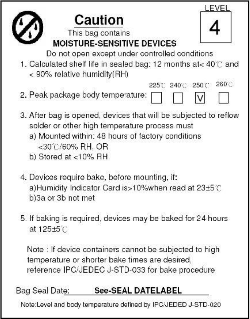
Label A Anti-static and humidity notice
Label B MSL caution / Storage Condition
Label C Inner box label .
Label D Carton box label .

AP6212 Datasheet
22
13.2 Dimension

AP6212 Datasheet
23
A
B
C
Humidity indicator
Desiccant
C
D
AP6212 Datasheet
24
13.3 MSL Level / Storage Condition
※NOTE : Accumulated baking time should not exceed 96hrs
Regulatory Notices
1. FCC
FCC Part 15.19 Statements:
This device complies with Part 15 of the FCC Rules. Operation is subject to the following two
conditions: (1) this device may not cause harmful interference, and (2) this device must accept any
interference received, including interference that may cause undesired operation.
FCC Part 15.21 statement
Any changes or modifications not expressly approved by the party responsible for compliance could
void the user's authority to operate this equipment.
FCC Part 15.105 statement
This equipment has been tested and found to comply with the limits for a Class B digital device,
pursuant to part 15 of the FCC Rules.
These limits are designed to provide reasonable protection against harmful interference in a
residential installation. This equipment generates, uses and can radiate radio frequency energy and,
if not installed and used in accordance with the instructions, may cause harmful interference to
radio communications. However, there is no guarantee that interference will not occur in a particular
installation. If this equipment does cause harmful interference to radio or television reception, which
can be determined by turning the equipment off and on, the user is encouraged to try to correct
the interference by one or more of the following measures:
- Reorient or relocate the receiving antenna.
- Increase the separation between the equipment and receiver.
- Connect the equipment into an outlet on a circuit different from that to which the receiver
is connected.
Consult the dealer or an experienced radio/TV technician for help.
OEM Responsibilities to comply with FCC and Industry Canada Regulations
The module has been certified for integration into products only by OEM integrators under the
following condition:
- The antenna(s) must be installed such that a minimum separation distance of at least 20 cm is
maintained between the radiator (antenna) and all persons at all times.
- The transmitter module must not be co-located or operating in conjunction with any other antenna
or transmitter except in accordance with FCC multi-transmitter product procedures.
As long as the two condition above is met, further transmitter testing will not be required. However,
the OEM integrator is still responsible for testing their end-product for any additional compliance
requirements required with this module installed (for example, digital device emissions, PC
peripheral requirements, etc.).
End Product Labeling
The module is labeled with its own FCC ID. If the FCC ID is not visible when the module is
installed inside another device, then the outside of the device into which the module is installed
must also display a label referring to the enclosed module. In that case, the final end product must
be labeled in a visible area with the following:
“Contains FCC ID: 2AI4I-AP6212